1
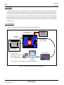
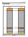
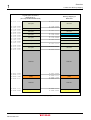
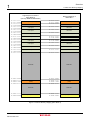
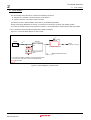
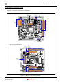
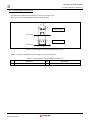
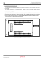
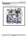
REJ10J1262-0101 SH7211 CPU Board M3A-HS11 32 User's Manual Renesas 32-Bit RISC Microcomputers SuperH RISCengine Family / SH7211 Group TM Rev. 1.01 Issued : Jan 31, 2008 Notes regarding these materials 1. This document is provided for reference purposes only so that Renesas customers may select the appropriate Renesas products for their use. Renesas neither makes warranties or representations with respect to the accuracy or completeness of the information contained in this document nor grants any license to any intellectual property rights or any other rights of Renesas or any third party with respect to the information in this document. 2. Renesas shall have no liability for damages or infringement of any intellectual property or other rights arising out of the use of any information in this document, including, but not limited to, product data, diagrams, charts, programs, algorithms, and application circuit examples. 3. You should not use the products or the technology described in this document for the purpose of military applications such as the development of weapons of mass destruction or for the purpose of any other military use. When exporting the products or technology described herein, you should follow the applicable export control laws and regulations, and procedures required by such laws and regulations. 4. All information included in this document such as product data, diagrams, charts, programs, algorithms, and application circuit examples, is current as of the date this document is issued. Such information, however, is subject to change without any prior notice. Before purchasing or using any Renesas products listed in this document, please confirm the latest product information with a Renesas sales office. Also, please pay regular and careful attention to additional and different information to be disclosed by Renesas such as that disclosed through our website. (http://www.renesas.com ) 5. Renesas has used reasonable care in compiling the information included in this document, but Renesas assumes no liability whatsoever for any damages incurred as a result of errors or omissions in the information included in this document. 6. When using or otherwise relying on the information in this document, you should evaluate the information in light of the total system before deciding about the applicability of such information to the intended application. Renesas makes no representations, warranties or guaranties regarding the suitability of its products for any particular application and specifically disclaims any liability arising out of the application and use of the information in this document or Renesas products. 7. With the exception of products specified by Renesas as suitable for automobile applications, Renesas products are not designed, manufactured or tested for applications or otherwise in systems the failure or malfunction of which may cause a direct threat to human life or create a risk of human injury or which require especially high quality and reliability such as safety systems, or equipment or systems for transportation and traffic, healthcare, combustion control, aerospace and aeronautics, nuclear power, or undersea communication transmission. If you are considering the use of our products for such purposes, please contact a Renesas sales office beforehand. Renesas shall have no liability for damages arising out of the uses set forth above. 8. Notwithstanding the preceding paragraph, you should not use Renesas products for the purposes listed below: (1) artificial life support devices or systems (2) surgical implantations (3) healthcare intervention (e.g., excision, administration of medication, etc.) (4) any other purposes that pose a direct threat to human life Renesas shall have no liability for damages arising out of the uses set forth in the above and purchasers who elect to use Renesas products in any of the foregoing applications shall indemnify and hold harmless Renesas Technology Corp., its affiliated companies and their officers, directors, and employees against any and all damages arising out of such applications. 9. You should use the products described herein within the range specified by Renesas, especially with respect to the maximum rating, operating supply voltage range, movement power voltage range, heat radiation characteristics, installation and other product characteristics. Renesas shall have no liability for malfunctions or damages arising out of the use of Renesas products beyond such specified ranges. 10. Although Renesas endeavors to improve the quality and reliability of its products, IC products have specific characteristics such as the occurrence of failure at a certain rate and malfunctions under certain use conditions. Please be sure to implement safety measures to guard against the possibility of physical injury, and injury or damage caused by fire in the event of the failure of a Renesas product, such as safety design for hardware and software including but not limited to redundancy, fire control and malfunction prevention, appropriate treatment for aging degradation or any other applicable measures. Among others, since the evaluation of microcomputer software alone is very difficult, please evaluate the safety of the final products or system manufactured by you. 11. In case Renesas products listed in this document are detached from the products to which the Renesas products are attached or affixed, the risk of accident such as swallowing by infants and small children is very high. You should implement safety measures so that Renesas products may not be easily detached from your products. Renesas shall have no liability for damages arising out of such detachment. 12. This document may not be reproduced or duplicated, in any form, in whole or in part, without prior written approval from Renesas. 13. Please contact a Renesas sales office if you have any questions regarding the information contained in this document, Renesas semiconductor products, or if you have any other inquiries. Table of Contents Chapter1 Overview .............................................................................................................................. 1-1 1.1 Overview .................................................................................................................................................................... 1-2 1.2 Configuration .............................................................................................................................................................. 1-2 1.3 External Specifications ............................................................................................................................................... 1-3 1.4 External View ............................................................................................................................................................. 1-4 1.5 M3A-HS11 Block Diagram.......................................................................................................................................... 1-5 1.6 M3A-HS11 Board Overview ....................................................................................................................................... 1-6 1.7 M3A-HS11 Memory Mapping ..................................................................................................................................... 1-8 1.8 Absolute Maximum Ratings...................................................................................................................................... 1-11 1.9 Recommended Operating Conditions ...................................................................................................................... 1-11 Chapter2 Functional Overview ............................................................................................................ 2-1 2.1 Functional Overview................................................................................................................................................... 2-2 2.2 CPU............................................................................................................................................................................ 2-3 2.3 Memory ...................................................................................................................................................................... 2-4 2.3.1 SH7211 On-Chip Memory ................................................................................................................................. 2-4 2.3.2 SDRAM ............................................................................................................................................................. 2-4 2.3.3 SRAM................................................................................................................................................................ 2-8 2.3.4 EEPROM......................................................................................................................................................... 2-11 2.4 Serial Port Interface.................................................................................................................................................. 2-12 2.5 I/O Ports ................................................................................................................................................................... 2-13 2.6 Power Supply Circuit ................................................................................................................................................ 2-15 2.7 Clock Module............................................................................................................................................................ 2-16 2.8 Reset Module ........................................................................................................................................................... 2-17 2.9 Interrupt Switches..................................................................................................................................................... 2-17 2.10 E10A-USB Interface ............................................................................................................................................... 2-18 Chapter 3 Operational Specifications .................................................................................................. 3-1 3.1 M3A-HS11 Connectors Outline .................................................................................................................................. 3-2 3.1.1 H-UDI Connector (J1, J2).................................................................................................................................. 3-3 3.1.2 Serial Port Connector (J3)................................................................................................................................. 3-5 3.1.3 Power Supply Connector (J4) ........................................................................................................................... 3-6 3.1.4 External Power Supply Connector for SH7211 (J5, J6)..................................................................................... 3-7 3.1.5 A/D, D/A Connector (J7).................................................................................................................................... 3-8 3.1.6 Extension Connectors (J8-J12) ......................................................................................................................... 3-9 3.2 Outline of Switches and LEDs .................................................................................................................................. 3-15 3.2.1 SH7211 Power Supply Select Jumpers (JP1, JP2)......................................................................................... 3-16 3.2.2 AVCC and AVREF Select Jumper (JP3, JP4)................................................................................................. 3-17 3.2.3 Switch and LED Functions .............................................................................................................................. 3-18 3.3 Board Dimensions of M3A-HS11.............................................................................................................................. 3-20 Rev. 1.01 Jan 31, 2008 REJ10J1262-0101 (i) Appendix..............................................................................................................................................A-1 M3A-HS11 SCHEMATICS Rev. 1.01 Jan 31, 2008 REJ10J1262-0101 (ii) Chapter1Overview Chapter1 Overview 1-1 Overview 1 1.1 Overview 1.1 Overview The M3A-HS11 is the CPU board designed for users to evaluate the functionality and performance of the SH7211 group of Renesas Technology original microcomputers, as well as develop and evaluate the application software for this group of microcomputers. The SH7211's data bus, address bus and various internal peripheral circuit function pins are connected to the extension connector of the M3A-HS11, allowing users to evaluate the timing relationship with peripheral devices using measurement instruments or develop extension boards tailored to suit development purposes. Furthermore, the E10A-USB or the on-chip emulator made by Renesas Technology can also be connected to the M3A-HS11. 1.2 Configuration Figure1.2.1 shows an example of system configuration using the M3A-HS11. DC 5V Power Supply (1.5A min.) SH7211 CPU Board M3A-HS11 * Serial Port Connector H-UDI Connector (14pin or 36pin) SH7211 Extension Board *Can be created according to applications High-performance * Embeded Workshop(HEW) HEW debugger SuperH RISC engine * C/C++ compiler package E10A-USB * USB * Host Computer * :It is necessary to by separately for software development. Figure1.2.1 Example System Configuration of M3A-HS11 Rev.1.01 Jan 31, 2008 REJ10J1262-0101 1-2 Overview 1 1.3 External Specifications 1.3 External Specifications Table1.3.1 lists external specifications of M3A-HS11. Table1.3.1 External Specifications of M3A-HS11 No. Item Content SH7211 1 CPU • Input(XIN) Clock : 10MHz • CPU Clock : 160MHz,max • Bus Clock : 40MHz,max • On-chip memory Flash Memory : 512KB RAM : 32KB • SDRAM : 16-Mbyte EDS1216AATA-75E 1pc. (16-bit bus width) 2 Memory • SRAM : 2-Mbyte (SRAM with byte selection) R1LV1616RSA7S 1pc. (16-bit bus width) • EEPROM : 128k-bit 2 HN58X24128FPIE 1pc. (I C Bus Connection) 3 Connector 4 LED 5 Switch 6 Package Dimension Rev.1.01 Jan 31, 2008 REJ10J1262-0101 • Extension Connector(Bus, I/O, VCC, GND) • A/D, D/A Connector (AN0~7,DA0~1,AVcc,AVss,AVref,AVrefvss) • Serial Port Connector (D-sub 9pins) • H-UDI connector (14pins) • H-UDI connector (36pins) • POWER LED (1pc.) • User LED (6pcs.) • Reset Switch (1pc.) • NMI Switch (1pc.) • IRQ3 Switch (1pc.) • TP Switch (1pc.) • DIP Switch for System Setting (1pc., 3 poles) • DIP Switch for User (1pc., 4 poles) • Dimensions :100mm x 100mm • Mounting Form :6-layer, Double-Side Mounted • Board Configuration :1 board 1-3 Overview 1 1.4 External View 1.4 External View Figure1.4.1 shows the external view of M3A-HS11. Figure1.4.1 External View of M3A-HS11 Rev.1.01 Jan 31, 2008 REJ10J1262-0101 1-4 Overview 1 1.5 M3A-HS11 Block Diagram 1.5 M3A-HS11 Block Diagram Figure1.5.1 shows the system block diagram of M3A-HS11. Figure1.5.1 System Block Diagram of M3A-HS11 Rev.1.01 Jan 31, 2008 REJ10J1262-0101 1-5 Overview 1 1.6 M3A-HS11 Board Overview 1.6 M3A-HS11 Board Overview Figure1.6.1 shows the M3A-HS11 board overview. < Top view of the component side > JP3 AVCC Select Jumper JP4 AVREF Select Jumper J7 A/D,D/A Connector (Not mounted) SW4 DIP Switch for System Setting J4 SW1 Power Power Switch Supply Connector LED1 Power LED J3 Serial Port Connector J1 H-UDI Connector (36-pin) U1 SH7211 LED2-7 User LED J2 H-UDI Connector (14-pin) SW2 Reset Switch SW3 DIP Switch SW5 NMI Switch JP1,JP2 Power Supply Select Jumper SW6 IRQ3 Switch J5,J6 SW7 External TP Switch Power Supply Connector (Not mounted) < Top view of the solder side > J11 Extension Connector (Not mounted) J12 Extension Connector (Not mounted) U7 U8 J10 Extension Connector (Not mounted) U5 U3 J8 Extension Connector (Not mounted) J9 Extension Connector (Not mounted) Figure1.6.1 M3A-HS11 Board Overview Rev.1.01 Jan 31, 2008 REJ10J1262-0101 1-6 Overview 1 1.6 M3A-HS11 Board Overview Table1.6.1 lists main components mounted in the M3A-HS11. Table1.6.1 Main Components Mounted in the M3A-HS11 Symbol Parts Name Remarks Recommended Parts Number for Not-Mounted Components U1 CPU SH7211 (Renesas) U2 Clock Buffer Not mounted U3 SRAM R1LV1616RSA7S U4 EEPROM HN58X24128FPIE U5 SDRAM EDS1216AATA-75E U6 RS-232C Driver SP3232ECA(Sipex) U7 3.3V Voltage Regulator LMS1587CSX-ADJ(NS) U8 1.5V Voltage Regulator LMS1587CSX-ADJ(NS) U9 Reset IC M51957BFP (Renesas) U10, U11 Logic IC X1 Oscillator 10.00MHz X2 Ceramic Resonator Not mounted J1 H-UDI Connector 36-pin type J2 H-UDI Connector 14-pin type J3 Serial Port Connector J4 Power Supply Connector J5 External Power Supply Connector Not mounted A2-2PA-2.54DSA (Hirose) J6 External Power Supply Connector Not mounted A2-3PA-2.54DSA (Hirose) J7 A/D, D/A Connector Not mounted 7614-6002 (Sumitomo 3M) J8, J10, J11 Extension Connector Not mounted XG4C-2031 (Omron) J9, J12 Extension Connector Not mounted XG4C-4031 (Omron) LED1 Power LED Red LED2-7 User LED Green SW1 Power Switch SW2 Reset Switch SW3 DIP Switch for User SW4 DIP Switch for System Setting SW5 NMI Switch SW6 IRQ3 Switch SW7 TP Switch Rev.1.01 Jan 31, 2008 REJ10J1262-0101 CY2305SC-1 (Cypress) CSTCE-G10M0 (Murata) 1-7 Overview 1 1.7 M3A-HS11 Memory Mapping 1.7 M3A-HS11 Memory Mapping Figure1.7.1, Figure1.7.2 and Figure1.7.3 show the SH7211 memory mapping examples in the M3A-HS11 on each MCU mode. Logical Space of SH7211 MCU Mode 3 (Single Chip Mode) H'0000 0000 Memory Mapping of M3A-HS11 H'0000 0000 On-Chip ROM (512KB) On-Chip ROM (512KB) H'0007 FFFF H'0008 0000 H'0007 FFFF H'0008 0000 Reserved H'FFF7 FFFF H'FFF8 0000 H'FFF8 7FFF H'FFF8 8000 On-Chip RAM (32KB) Reserved H'FFF7 FFFF H'FFF8 0000 H'FFF8 7FFF H'FFF8 8000 Reserved Reserved H'FFFC 0000 H'FFFC 0000 On-Chip Peripheral Module On-Chip Peripheral Module H'FFFF FFFF On-Chip RAM (32KB) H'FFFF FFFF Figure1.7.1 SH7211Memory Mapping (MCU Mode 3) Rev.1.01 Jan 31, 2008 REJ10J1262-0101 1-8 Overview 1 1.7 M3A-HS11 Memory Mapping Logical Space of SH7211 MCU Mode 0,1 (On-Chip ROM Disabled Mode) H'0000 0000 Memory Mapping of M3A-HS11 H'0000 0000 CS0 Space H'03FF H'0400 H'07FF H'0800 H'0BFF H'0C00 H'0FFF H'1000 H'13FF H'1400 H'17FF H'1800 FFFF 0000 FFFF 0000 FFFF 0000 FFFF 0000 FFFF 0000 FFFF 0000 H'1BFF FFFF H'1C00 0000 CS1 Space CS2 Space CS3 Space CS4 Space CS5 Space CS6 Space CS7 Space H'1FFF FFFF H'2000 0000 User Area H'03FF FFFF H'0400 0000 H'0800 0000 H'0C00 H'0CFF H'1000 H'101F 0000 FFFF 0000 FFFF H'1400 0000 H'1800 0000 H'1C00 0000 H'FFF8 7FFF H'FFF8 8000 SDRAM(16MB) User Area SRAM(2MB) User Area User Area User Area User Area On-Chip RAM (32KB) Reserved H'FFF7 H'FFF8 H'FFF8 H'FFF8 FFFF 0000 7FFF 8000 Reserved H'FFFC 0000 H'FFFF FFFF User Area H'2000 0000 Reserved H'FFF7 FFFF H'FFF8 0000 User Area On-Chip Peripheral Module On-Chip RAM (32KB) Reserved H'FFFC 0000 H'FFFF FFFF On-Chip Peripheral Module Figure1.7.2 SH7211Memory Mapping (MCU Mode 0,1) Rev.1.01 Jan 31, 2008 REJ10J1262-0101 1-9 Overview 1 1.7 M3A-HS11 Memory Mapping Logical Space of SH7211 MCU Mode 2 (On-Chip ROM Enabled Mode) H'0000 H'0007 H'0008 H'01FF H'0200 H'03FF H'0400 0000 FFFF 0000 FFFF 0000 FFFF 0000 H'07FF FFFF H'0800 0000 H'0BFF H'0C00 H'0FFF H'1000 H'13FF H'1400 H'17FF H'1800 H'1BFF H'1C00 H'1FFF H'2000 FFFF 0000 FFFF 0000 FFFF 0000 FFFF 0000 FFFF 0000 FFFF 0000 On-Chip ROM (512KB) Reserved CS0 Space CS1 Space CS2 Space Memory Mapping of M3A-HS11 H'0000 0000 H'0007 FFFF H'0008 0000 H'0200 0000 H'0400 0000 H'0800 0000 CS3 Space H'0C00 0000 H'0CFF FFFF CS4 Space H'1000 0000 H'101F FFFF CS5 Space CS6 Space CS7 Space H'1400 0000 H'1800 0000 H'1C00 0000 FFFF 0000 7FFF 8000 User Area User Area User Area SDRAM (16MB) User Area SRAM (2MB) User Area User Area User Area User Area Reserved On-Chip RAM (32KB) H'FFF7 H'FFF8 H'FFF8 H'FFF8 FFFF 0000 7FFF 8000 On-Chip Peripheral Module On-Chip RAM (32KB) Reserved Reserved H'FFFC 0000 H'FFFF FFFF Reserved H'2000 0000 Reserved H'FFF7 H'FFF8 H'FFF8 H'FFF8 On-Chip ROM (512KB) H'FFFC 0000 H'FFFF FFFF On-Chip Peripheral Module Figure1.7.3 SH7211Memory Mapping (MCU Mode 2) Rev.1.01 Jan 31, 2008 REJ10J1262-0101 1-10 Overview 1 1.8 Absolute Maximum Ratings 1.8 Absolute Maximum Ratings Table1.8.1 lists the absolute maximum ratings of M3A-HS11. Table1.8.1 Absolute Maximum Ratings of M3A-HS11 Symbol Parameter Rated Value Remarks 5VCC 5V System Power Supply Voltage -0.3V to 6.0V Relative to VSS 3VCC 3.3V System Power Supply Voltage -0.3V to 4.6V Relative to VSS 1.5VCC 1.5V System Power Supply Voltage -0.3V to 2.3V Relative to VSS Operating Ambient Temperature -10°C to 55°C No dewdrops allowed. Topr Use in corrosive gas environment prohibited. Tstr Storage Ambient Temperature -20°C to 60°C No dewdrops allowed. Use in corrosive gas environment prohibited. Note: The ambient temperature refers to the air temperature in places closest possible to the board. 1.9 Recommended Operating Conditions Table1.9.1 lists the recommended operating conditions of M3A-HS11. Table1.9.1 Recommended Operating Conditions of M3A-HS11 Symbol Parameter 5VCC 5V System Power Supply Voltage 3VCC 1.5VCC - Rated Value Remarks 4.75V to 5.25V Relative to VSS 3.3V System Power Supply Voltage 3.0V to 3.6V Relative to VSS 1.5V System Power Supply Voltage 1.4V to 1.6V Relative to VSS Maximum Current Consumption in the Within 2A Board Topr Operating Ambient Temperature 0°C to 50°C No dewdrops allowed. Use in corrosive gas environment prohibited. Rev.1.01 Jan 31, 2008 REJ10J1262-0101 1-11 Overview 1 1.8 Absolute Maximum Ratings * This is a blank page * Rev.1.01 Jan 31, 2008 REJ10J1262-0101 1-12 Chapter2Functional Overview Chapter2 Functional Overview 2-1 2 Functional Overview 2.1 Functional Overview 2.1 Functional Overview The M3A-HS11 is the SH7211 CPU board that has the functions listed in Table2.1.1. Table2.1.1 lists the functional modules of M3A-HS11. Table2.1.1 Functional Modules of M3A-HS11 Section 2.2 Function CPU Content SH7211 • Input(XIN) Clock: 10 MHz • CPU Clock: Maximum 160 MHz, • Bus Clock: Maximum 40 MHz • On-Chip Memory - Flash Memory: 512 KB - RAM : 32 KB 2.3 Memory • SDRAM: 16-Mbyte EDS1216AATA-75E 1pc. (16-bit bus width) • SRAM : 2-Mbyte (SRAM with byte selection) R1LV1616RSA7S 1pc. (16-bit bus width) • EEPROM : 128k-bit 2 HN58X24128FPIE 1pc. (I C Bus Connection) 2.4 Serial Port Interface Connects SCI1 of the SH7211 to the serial port connector 2.5 I/O Ports Connects to the input/output ports of the SH7211 2.6 Power Supply Controls the system power supply of the M3A-HS11 2.7 Clock Module Controls the system clock 2.8 Reset Module Controls the device reset mounted on the M3A-HS11 2.9 Interrupt Switches Connect to the NMI pin, IRQ3 pin and test port 2.10 E10A-USB Interface SH7211 H-UDI/AUD interface Operational Specifications Connectors, Switches and LEDs - • SH7211 Extension Connector • Switches and LEDs • H-UDI Connector Detailed in Chapter 3. Rev.1.01 Jan 31, 2008 REJ10J1262-0101 2-2 2 Functional Overview 2.2 CPU 2.2 CPU The M3A-HS11 contains the 32-bit RISC microcomputer SH7211 that operates with a maximum 160MHz of CPU clock frequency. The SH7211 includes 512-Kbyte flash memory, and 32-Kbyte RAM, making it useful in a wide range of applications from data processing to equipment control. The M3A-HS11 can be operated with a maximum 160MHz of CPU clock frequency (external bus 40MHz, max) using a 10MHz input clock. Figure 2.2.1 shows the SH7211 block diagram in the M3A-HS11. SH7211 Clock Mode FWE MD1 MD0 MDCLK2 MDCLK0 System Control User LED PA0/A0 PA1/A1 PA2/A2 PA3/A3 PA4/A4 PA5/A5 PA6/A6 PA7/A7 PA8/A8 PA9/A9 PA10/A10 PA11/A11 PA12/A12 PA13/A13 PA14/A14 PA15/SCK3/A15 PA16/RXD3/A16 PA17/TXD3/A17 PA18/IRQ0/A18 PA19/IRQ1/A19 PA20/IRQ2/A20 PA21/IRQ3/A21 PA22/TIOC0A/IRQ4/A22 PA23/SCK1/TIOC0B/IRQ5/A23 Serial PA24/RXD1/TIOC0C/IRQ6/A24 Port PA25/TXD1/TIOC0D/IRQ7/A25 EXTAL XTAL PB3/CKIO Clock Mode 6 Fixed RES NMI WDTOVF PB10/RXD2/TIOC4CS/WAIT/DREQ3 PB11/TXD2/TIOC4DS/AH/DACK3 PB12/TXD2/TIOC4AS/BREQ PB13/SCK2/TIOC4BS/BACK PB20/TIOC3DS/BS PB21/TIOC3BS/RXD0/IRQ0/CS2 DIP Switch for User PB15/TIOC3C/IRQ5/CS5 PB19/TIOC3D/IRQ6/CS6 PB28/RXD3/TIOC1A/DACK0 PB29/TIOC1B/DREQ0 EEPROM I/F PF0/SCL/POE7/IRQ0 PF1/SDA/POE3/IRQ1 PB0/RXD0/POE0/RD PB1/TXD0/POE8/RD/WR PB2/SCK0/POE4/CS0 PB4/TIOC4A/CKE PB5/TIOC4B/IRQ2/RASL PB6/TIOC4C/IRQ3/CASL PB7/TIOC4D/IRQ7/CS7 PB8/RXD3/TIOC3AS/WE0/DQMLL PB9/TXD3/TIOC3CS/WE1/WE/DQMLU PB14/RXD2/ADTRG/MRES PB16/TXD0/POE1/CS1 PB17/TIOC3A/IRQ1/CS3 PB18/TIOC3B/IRQ4/CS4 A/D AN0 AN1 AN2 AN3 AN4 AN5 AN6 AN7 D/A DA0 DA1 PD0/D0 PD1/D1 PD2/D2 PD3/D3 PD4/D4 PD5/D5 PD6/D6 PD7/D7 PD8/D8 PD9/D9 PD10/D10/TIC5W PD11/D11/TIC5V PD12/D12/TIC5U PD13/D13/TIC5WS PD14/D14/TIC5VS PD15/D15/TIC5US TDI TDO TCK TMS TRST ASEMD PB30/ASEBRKAK/ASEBRK/UBCTRG/IRQOUT PB22/AUDSYNC/RXD2/TCLKD/DACK2/FRAME PB23/AUDCK/TXD2/TCLKC/DREQ2 PB24/AUDATA3/RXD3/TCLKB/IRQ2/TEND1 PB25/AUDATA2/TXD3/TCLKA/IRQ3/DACK1 PB26/AUDATA1/SCK3/TIOC2B/DREQ1 PB27/AUDATA0/TXD3/TIOC2A/TEND0 Address Bus Data Bus H-UDI AUD Figure 2.2.1 SH7211 Block Diagram Rev.1.01 Jan 31, 2008 REJ10J1262-0101 2-3 2 Functional Overview 2.3 Memory 2.3 Memory 2.3.1 SH7211 On-Chip Memory The SH7211 includes 512-Kbyte flash memory and 32-Kbyte RAM. 2.3.2 SDRAM The M3A-HS11 mounts 16MB SDRAM as standard equipment. The SDRAM is controlled by the bus state controller built into SH7211. Table2.3.1 lists the SDRAM specifications used in M3A-HS11. Figure 2.3.1 shows the block diagram of SDRAM connection. Table2.3.1 SDRAM Specifications Specification Content Part Number EDS1216AATA-75E Configuration 16 Mbytes (16-bit bus width) x 1pc. Capacity 16 Mbytes Access Time 5.4ns CAS Latency 2 (at 40 MHz bus clock) Refresh Interval 4,096 refresh cycles every 64ms Low Address A11- A0 Column Address A8 - A0 Number of Banks 4-bank operation controlled by BA0 and BA1 EDS1216AATA SH7211 (8M Word x 16bit) A14 A13 A12-A1 11 BA1 BA0 BA0 A11-A0 -A0 A11 CK CKE CLK CKE CS3 CS# RASL AS R # RAS# CASL CAS# CAS RD/WR WE# DQMLU DQMU DQMLL D15-D0 16 DQML DQ15-DQ0 Figure 2.3.1 Block Diagram of SDRAM Connection Rev.1.01 Jan 31, 2008 REJ10J1262-0101 2-4 2 Functional Overview 2.3 Memory Table 2.3.2 lists the setting examples of bus state controller when the SH7211 bus clock is operating at 40 MHz. Table 2.3.2 Setting Examples of Bus State Controller (CS3 Space) User Area CS3 Target Device EDS1216AATA-75E SDRAM Controller Setting CS3 Space Bus Control Register(CS3BCR) Initial value: H'36DB 0600, Recommended set value: H'1000 4400 - Idle cycles between write-read cycles and write-write cycles IWW[2:0] = 001; 1 idle cycle inserted - Memory type TYPE[2:0] = 100; SDRAM - Data bus size BSZ[1:0] = 10; 16-bit size CS3 Space Wait Control Register(CS3WCR) Initial value: H'0000 0500, Recommended set value: H'0000 0000 0091 - Wait precharge completion cycle count WTRP[1:0] = 00; No wait cycle - Number of wait cycles from ACTV to READ/WRIT command WTRCD[1:0] = 00; No wait cycle - Area 3 CAS latency A3CL[1:0] = 01; 2 cycles - Number of command cycle from WRIT(A) to auto-precharge/PRE command TRWL[1:0] = 10; 2 cycles Number of command cycle from REF command/self-refresh release to ACTV command WTRC[1:0] =01; 3 cycles SDRAM Control Register(SDCR) Initial value: H'0000 0000, Recommended set value: H'0000 0809 - Refresh control RFSH = 1; Refresh is performed - Refresh control RMODE = 0; Auto-refreshing - Bank active mode BACTV = 0; Auto-precharge mode - Number of bits of row address for area3 A3ROW[1:0] = 01; 12 bits - Number of bits of column address for area3 A3COL[1:0] = 01; 9 bits Refresh Timer Control/Status Register(RTCSR) Initial value : H'0000 0000, Recommended set value : H’A55A 0010 - Clock select CKS[2:0] = 010 ;Bφ/16 - Refresh count RRC[2:0] = 000 ; Once Refresh Time Constant Register(RTCOR) Initial value: H'0000 0000, Recommended set value : H'A55A 0027 *The refresh request interval when clock select is set to Bφ/16 is as follows. 1 cycle :400nsec(40 MHz/16 = 2.5 MHz) Refresh request intervals in the SDRAM : 15.625µsec/time 15.625µsec /400nsec = 39(0x27) cycle / refresh counts Rev.1.01 Jan 31, 2008 REJ10J1262-0101 2-5 Functional Overview 2 2.3 Memory Figure 2.3.2 shows an example of SDRAM single read/write timing for operation that the SH7211 bus clock is operating at 40 MHz. SDRAM SINGLE READ SDRAM SINGLE WRITE tRC tRC tRCD tRCD tRAS tDPL tRP tRP tDAL tRAS tcyc (25ns) Tr Tc1 Tcw Td1 Tde Tr Tc1 Trwl1 Trwl2 ACT READA DESEL DESEL DESEL ACT WRITA DESEL DESEL CKIO CKE tCSD tCSD tSI tHI tCSD tSI tHI tCSD CS3 tRASD tRASD tSI RASL tSI tRASD tHI tCASD tRASD tHI tCASD tSI CASL tSI tCASD tHI tCASD tHI tRWD RDWR tSI tRWD tHI tDQMD1 tDQMD1 tDQMD1 tHI tSI tSI tDQMD1 tHI DQMUULL tAD1 tAD1 tAD1 tSI tAD1 tSI MA0-9,11 tAD1 tHI tAD1 tHI tAD1 MA10 tAD1 BA0-1 tRDS2 tAC D0-15 tRDH2 tOH tWDD 2 tSI tWDH2 tHI Data Figure 2.3.2 Example of SDRAM Single Read/Write Timing Rev.1.01 Jan 31, 2008 REJ10J1262-0101 2-6 2 Functional Overview 2.3.3 SRAM 2.3.3 SRAM The M3A-HS11 includes the 2-Mbyte SRAM as standard equipment. The SRAM is controlled by the bus state controller included in SH7211. Table2.3.3 lists the specification outline of SRAM. Figure 2.3.3 shows the block diagram of SH7211 and SRAM. Table2.3.3 SRAM Specification Outline Part Number Bus Size Capacity Package R1LV1616RSA-7S 16-bit 2-Mbyte (16-bit × 1M word × 1 pc.) 48-pin TSOP (20 ×12mm) R1LV1616RSA-7 SH7211 A20 - A1 D15 - D0 20 A19 - A0 16 DQ15 - DQ0 3.3V CS4 BYTE# CS1# Reset CS2 RD OE# RD/WR WE# WE1 UB# WE0 LB# 16M-bit SRAM (1M Word ×16bit) Figure 2.3.3 Block Diagram of SH7211 and SRAM Rev.1.01 Jan 31, 2008 REJ10J1262-0101 2-7 2 Functional Overview 2.3.3 SRAM Table2.3.4 lists the setting example of bus state controller when the bus clock of SH7211 is operating at 40 MHz. Table2.3.4 Setting Examples of Bus State Controller (CS4 Space) User Area CS4 Target Device R1LV1616RSA-7S SDRAM Controller Settings CS4 Space Bus Control Register : CS4BCR Initial value : H’36DB 0400, Recommended value : H'1659 3400 • Idle cycles between write-read cycles and write-write cycles IWW[2:0] = 001 ; 1 idle cycle inserted • Idle cycles for another space read-write IWRWD[2:0] = 011 ; 4 idle cycle inserted • Idle cycles for read-write in same space IWRWS[2:0] = 001 ; 1 idle cycle inserted • Idle cycles for another space read-read IWRRD[2:0] = 011 ; 4 idle cycle inserted • Idle cycles for read-read in same space IWRRS[2:0] = 001 ; 1 idle cycle inserted • Specify memory type TYPE[2:0] = 011 ; Byte selection SRAM • Specify data bus type BSZ[1:0] = 10 ; 16 bit bus width CS4 Space Wait Control Register : CS4WCR Initial value: H’0000 0500, Recommended value: H’ • Byte access selection for byte-selection SRAM BAS = 1 ; Asserts the WEn during the read/write access cycle and asserts the RDWR at the write timing. • Number of write access wait cycles WW[2:0] = 000 ; Same number of cycles as the number of read access wait • Number of delay cycles from address, CS4 assertion to RD, WEn assertion SW[1:0] = 01 ; 1.5 cycles • Number of read access wait cycles WR[3:0] = 0011 ; 3 cycles • External wait mask specification WM =1 ; External wait is ignored • Number of delay cycles from RD, WEn negation to address, CS4 negation HW[1:0] = 01;1.5 cycles Rev.1.01 Jan 31, 2008 REJ10J1262-0101 2-8 2 Functional Overview 2.3.3 SRAM Figure 2.3.4 shows the example of SRAM read timing when the bus clock is 40MHz and Figure 2.3.5 shows the example of SRAM write timing when the bus clock is 40MHz. tcyc (25ns) Th T1 Tw1 Tw2 Tw3 T2 Tf CKIO tRC tAD1 tAD1 tAA A20-A1 (A19-A0) tCHZ1 tCSD1 CS4 tACS1 (CS1) tWED2 tBHZ WEn tBA (UB,LB) RD/WR (WE) tRSD tRSD tOE RD (OE) tOHZ tOLZ tCLZ tOH tRDS1 tRDH1 D15-D0 Figure 2.3.4 Example of SRAM Read Timing tcyc (25ns) Th T1 Tw1 Tw2 Tw3 T2 Tf CKIO tWC tAD1 tAD1 A20-A1 (A19-A0) tCSD1 CS4 tCW (CS1) tWED2 WEn tBW (UB,LB) tAW tWR tAS tWP RD/WR tRWD1 tRWD1 (WE) tOW tDW tWDD1 tDH tWDH1 D15-D0 Figure 2.3.5 Example of SRAM Write Timing Rev.1.01 Jan 31, 2008 REJ10J1262-0101 2-9 2 Functional Overview 2.3.4 EEPROM 2.3.4 EEPROM The M3A-HS11 includes the 128k-bit EEPROM as standard equipment. The EEPROM is controlled by the I2C bus interface included in SH7211. Table 2.3.5 lists the specification outline of EEPROM. Figure 2.3.6 shows the connection circuit block diagram of SH7211 and EEPROM. Table 2.3.5 EEPROM Specification Outline Part Number Interface Capacity Package HN58X24128FPIE 2-wire system serial (I2C bus)*1 128 k-bit (16k-word × 8-bit) 8-pin SOP SH7211 HN58X24128FPIE PF0/SCL SCL A0 A1 PF1/SDA SDA WP A2 128k-bit EEPROM Figure 2.3.6 Block Diagram of SH7211 and EEPROM 2 Note*1: I C bus is a trademark of Koninklijke Philips Electronics N. V. Rev.1.01 Jan 31, 2008 REJ10J1262-0101 2-10 2 Functional Overview 2.4 Serial Port Interface 2.4 Serial Port Interface In the M3A-HS11, the SCI channel 1 of SH7211 is connected to the serial port connector (J3). Figure 2.4.1 shows the block diagram of serial port interface in the M3A-HS11. SH7211 Serial Port Connector (J3) RS-232C Driver N C PA24/RXD1 PA25/TXD1 1 2 3 4 DCD RxD TxD DTR GN 5 GND D 6 DSR 7 RTS 8 CTS N 9 RI C Figure 2.4.1 Block Diagram of Serial Port Interface Rev.1.01 Jan 31, 2008 REJ10J1262-0101 2-11 2 Functional Overview 2.5 I/O Ports 2.5 I/O Ports In the M3A-HS11, all of the SH7211's I/O ports are connected to the extension bus connector. Some I/O ports are connected to DIP switches and LEDs of the M3A-HS11 board. Users are free to use these ports. Figure 2.5.1 shows the block diagram of DIP Switch and LEDs in the M3A-HS11. Table 2.5.1 lists the functions of the SH7211 I/O ports in the M3A-HS11. 3VCC H11 H10 LED7 Green H9 LED6 Green H8 LED5 Green H7 LED4 Green H6 LED3 Green LED2 Green SH7211 PB10/TIOC4CS PB11/TIOC4DS PB12/TIOC4AS PB13/TIOC4BS PB20/TIOC3DS PB21/TIOC3BS VCC DIP Switch for User (SW3) SW3-1 SW3-2 SW3-3 SW3-4 PB15 PB19 PB28 PB29 Figure 2.5.1 Block Diagram of DIP Switch and LEDs in M3A-HS11 Rev.1.01 Jan 31, 2008 REJ10J1262-0101 2-12 2 Functional Overview 2.5 I/O Ports Table 2.5.1 Functions of SH7211 I/O Ports SH7211 Port Name Connection in M3A-HS11 PA0 Extension Connector (J8, J9) PA1 - PA9 Extension Connector (J8, J9), SDRAM, SRAM PA10 - PA14 Extension Connector (J9), SDRAM, SRAM PA15 - PA20 Extension Connector (J9), SRAM PA21 Extension Connector (J9), IRQ3 Switch PA22 Extension Connector (J9, J10) PA23 Extension Connector (J9, J12) PA24 - PA25 Extension Connector (J9), Serial Port Connector PB0 Extension Connector (J11, J12) , SRAM PB1 Extension Connector (J10), SDRAM, SRAM PB2 Extension Connector (J8, J9, J12) PB3 Extension Connector (J8, J9), SDRAM PB4 - PB6 Extension Connector (J10), SDRAM PB7 Extension Connector (J10, J12) PB8 - PB9 Extension Connector (J10), SDRAM, SRAM PB10 Extension Connector (J10, J12), LED PB11 Extension Connector (J10), LED PB12 - PB13 Extension Connector (J10, J12), LED PB14 Extension Connector (J12) PB15 Extension Connector (J8, J9, J12), DIP Switch for User PB16 Extension Connector (J8, J9) PB17 Extension Connector (J10), SDRAM PB18 Extension Connector (J8, J9), SRAM PB19 Extension Connector (J10), DIP Switch for User PB20 Extension Connector (J12), LED PB21 Extension Connector (J8, J9), LED PB22 - PB27, PB30 (It is possible to connect to the extension connector (J12) by mounting the resistance) PB28 - PB29 Extension Connector (J12), DIP Switch for User PD0 - PD15 Extension Connector (J11, J12) PF0 - PF1 Extension Connector (J10), EEPROM Rev.1.01 Jan 31, 2008 REJ10J1262-0101 2-13 2 Functional Overview 2.6 Power Supply Circuit 2.6 Power Supply Circuit In the M3A-HS11, the 5V power supply is input to the board and it generates 3.3V and 1.5V by using a regulator. The used regulator uses an output voltage-controlled type so that a desired voltage value can be generated by changing the resistance. Figure 2.6.1 shows the block diagram of power supply circuit in the M3A-HS11. Extension Connector A/D,D/A Connector (J7) 5VCC AVCC AVCC JP1 A/D,D/A Connector (J7) 5VCC AVREF AVREF JP2 External Power Supply (J5) 5V Power Switch 1.5VCC_EX 5VCC 5V 1.5V JP 1.5VCC 1.5VCC_CPU VCC External Power Supply (J6) 3VCC_EX 5VCC 5V 3.3V JP 3VCC 3VCC_CPU VCCQ SH7211 SDRAM SRAM Extension Connector Figure 2.6.1 Block Diagram of Power Supply Circuit Rev.1.01 Jan 31, 2008 REJ10J1262-0101 2-14 2 Functional Overview 2.7 Clock Module 2.7 Clock Module The clock module in the M3A-HS11 consists of the following two blocks: • • Output from a oscillator connected to EXTAL of the SH7211 Ceramic resonator connected to EXTAL and XTAL The M3A-HS11 has a 10MHz oscillator connected to it as standard specification. System clock output (PB3/CKIO) of SH7211 is connected to an extension connector with dumping resistor. To connect an extension board to the extension connector, it is recommended to install a clock buffer that contains a PLL to ensure that the board will be supplied with a stable clock signal. Figure 2.7.1 shows the block diagram of clock module. Rb *2 Oscillator CLK Ra *1 SH7211 EXTAL Clock Buffer *2 EXCLK (Extension Connector) PB3/CKIO XTAL Ceramic Resonators *1 10MHz CY2305SC-1H(Cypress) PB3/CKIO(SDRAM Clock) *1:To mount the ceramic oscillator, remove the resistance Ra. *2:To mount the clock buffer, remove the resistance Rb. Not mounted Figure 2.7.1 Block Diagram of Clock Module Rev.1.01 Jan 31, 2008 REJ10J1262-0101 2-15 2 Functional Overview 2.8 Reset Module 2.8 Reset Module This circuit controls the reset signal of SH7211 mounted on the M3A-HS11. Figure 2.8.1 shows the block diagram of reset module in the M3A-HS11. R1LV1616RSA-7S Reset IC Output Delay Time : td = 0.34 × Cd(pF) = 34ms Reset IC Output Detection Voltage : Ra=10KΩ,Rb=10KΩ Vs = 1.25 × (Ra+Rb)/Rb = 2.5V CS2 Extension Connector 3Vcc 3Vcc RESET Ra Rb M51957BP SH7211 Input RES Output Delay Capacitance Cd 0.1uF Reset Switch (SW2) Figure 2.8.1 Block Diagram of Reset Module 2.9 Interrupt Switches In the M3A-HS11, the push switches are connected with the IRQ3 (PA21) pin and NMI pin of the SH7211. Moreover, TP switch is connected with the test port (H12) so that it can be used by connecting with a desired pin. Figure 2.9.1 shows the block diagram of interrupt switch in the M3A-HS11. 3VCC SH7211 NMI SW5 NMI Switch 3VCC PA21/IRQ3 SW6 IRQ3 Switch 3VCC TP H12 SW7 TP Switch Figure 2.9.1 Block Diagram of Interrupt Switch Rev.1.01 Jan 31, 2008 REJ10J1262-0101 2-16 2 Functional Overview 2.10 E10A-USB Interface 2.10 E10A-USB Interface The M3A-HS11 has the H-UDI connectors (14-pin and 36-pin) to connect with E10A-USB. Figure 2.10.1 shows the block diagram of E10A-USB interface. VccQ VccQ VccQ H-UDI Connector (36-pin) 2 4 6 8 10 GND AUDCK GND AUDATA0 GND AUDATA1 GND AUDATA2 GND 12 GND 14 GND 16 GND 18 GND 20 GND 22 (GND) 24 GND 26 GND 28 GND 30 GND 32 GND 34 GND 36 GND AUDATA3 AUDSYNC N.C. N.C. TCK TMS TRST TDI TDO ASEBRKAK/ASEBRK UVCC RES GND N.C. SH7211 1 3 5 7 9 11 13 9 TRST GND 12 GND 13 GND 14 GND AUDATA1 AUDATA2 AUDATA3 AUDSYNC 17 19 21 23 25 27 29 TCK TMS TRST TDI TDO ASEBRKAK/ASEBRK 31 33 35 ASEMD RES TCK (GND) AUDATA0 15 H-UDI Connector (14-pin) 10 AUDCK TDO ASEBRKAK/ASEBRK TMS TDI RES N.C. UVCC 1 2 3 4 5 6 7 8 Reset Signal 11 Figure 2.10.1 Block Diagram of E10A-USB Interface Rev.1.01 Jan 31, 2008 REJ10J1262-0101 2-17 2 Functional Overview 2.10 E10A-USB Interface This is a blank page Rev.1.01 Jan 31, 2008 REJ10J1262-0101 2-18 Chapter 3 Operational Specifications Chapter 3 Operational Specifications 3-1 Operational Specifications 3 3.1 M3A-HS11 Connectors Outline 3.1 M3A-HS11 Connectors Outline Figure 3.1.1 shows M3A-HS11 connector assignments. <Top View of the Component Side > J7 A/D,D/A Connector (Not mounted) J4 Power Supply Connector J3 Serial Port Connector J1 H-UDI Connector (36-pin) J2 H-UDI Connector (14-pin) J5,J6 External Power Supply Connector (Not mounted) < Top View of the Solder Side > J11 Extension Connector (Not mounted) J12 Extension Connector (Not mounted) J10 Extension Connector (Not mounted) J8 Extension Connector (Not mounted) J9 Extension Connector (Not mounted) Figure 3.1.1 M3A-HS11 Connector Assignments Rev.1.01 Jan 31, 2008 REJ10J1262-0101 3-2 Operational Specifications 3 3.1.1 H-UDI Connector (J1, J2) 3.1.1 H-UDI Connector (J1, J2) The M3A-HS11 includes a 36-pin H-UDI (J1) connector and 14-pin H-UDI (J2) connector for a connection to the E10A-USB emulator. Figure 3.1.2 shows a pin assignment of H-UDI (J1) connector. 35 1 36 2 Top View of the Component Side Board Edge Side View Board Edge Figure 3.1.2 Pin Assignment of H-UDI(J1) Connector Table 3.1.1 lists pin assignments of H-UDI connector (J1). Table 3.1.1 Pin Assignments of H-UDI (J1) Connector Pin 1 2 Signal Name Pin Signal Name AUDCK 19 TMS GND GND 20 3 AUDATA0 21 TRST 4 GND 22 (GND) 5 AUDATA1 23 TDI 6 GND 24 GND 7 AUDATA2 25 TDO 8 GND 26 GND 9 AUDATA3 27 ASEBRKAK/ASEBRK 10 GND 28 GND UVCC ________________ _________ ___________________ ______________ 11 AUDSYNC 29 12 GND 30 GND 13 NC 31 RES 14 GND 32 GND 15 NC 33 GND 16 GND 34 GND TCK 35 NC GND 36 GND 17 18 Rev.1.01 Jan 31, 2008 REJ10J1262-0101 _______ 3-3 Operational Specifications 3 3.1.1 H-UDI Connector (J1, J2) Figure 3.1.3 shows a pin assignment of H-UDI (J2) connector. 7 6 5 4 3 2 1 14 13 12 11 10 9 8 Board Edge Top View of the Component Side J2 Side View Board Edge Figure 3.1.3 Pin Assignment of H-UDI (J2) Connector Table 3.1.2 lists pin assignments of H-UDI (J2) connector. Table 3.1.2 Pin Assignments of H-UDI (J2) Connector Pin 1 Signal Name TCK _________ Pin Signal Name 8 NC 2 TRST 9 (GND) 3 TDO 10 GND ___________________ ______________ 4 ASEBRKAK/ASEBRK 11 UVCC 5 TMS 12 GND 6 TDI 13 GND 14 GND 7 _______ RES Rev.1.01 Jan 31, 2008 REJ10J1262-0101 3-4 Operational Specifications 3 3.1.2 Serial Port Connector (J3) 3.1.2 Serial Port Connector (J3) The M3A-HS11 includes a serial port connector (J3). Figure3.1.4 shows a pin assignment of serial port connector. 1 6 5 9 Board Edge Top View of the Component Side 1 6 5 9 Board Edge Side View Figure3.1.4 Pin Assignment of Serial Port Connector (J3) Table 3.1.3 lists pin assignments of serial port connector. Table 3.1.3 Pin Assignments of Serial Port Connector (J3) Pin Signal Name Pin Signal Name _______ 1 NC 6 DSR _______ 2 RXD 7 RTS _______ 3 TXD 8 CTS 9 NC _______ 4 DTR 5 GND Pins 4-6 are loop back connected. Pins 7-8 are loop back connected. Rev.1.01 Jan 31, 2008 REJ10J1262-0101 3-5 Operational Specifications 3 3.1.3 Power Supply Connector (J4) 3.1.3 Power Supply Connector (J4) The M3A-HS11 includes the power supply connector pin for the SH7211. Figure 3.1.5 shows a pin assignment of power supply connector. GND +5V 1 2 1 2 Top View of the Component Side Board Edge Side View Board Edge Figure 3.1.5 Pin Assignment of Power Supply Connector (J4) Table 3.1.4 lists a pin assignment of power supply connector for M3A-HS11. Table 3.1.4 Pin Assignment of Power Supply Connector (J4) Pin 1 Signal Name + 5V Rev.1.01 Jan 31, 2008 REJ10J1262-0101 Pin 2 Signal Name GND 3-6 Operational Specifications 3 3.1.4 External Power Supply Connector for SH7211 (J5, J6) 3.1.4 External Power Supply Connector for SH7211 (J5, J6) The M3A-HS11 includes the external power supply connector pins to supply the power source of 3.3V and 1.5V externally. When the power is supplied by using this connector, set the power select jumper (JP1 and JP2) to “2-3”. Figure 3.1.6 shows a pin assignment of power supply connector. Top View of the Component Side J5 1 1.5V 3.3V J6 21 2 Board Edge Figure 3.1.6 Pin Assignment of Power Supply Connector (J5, J6) Table 3.1.5 lists a pin assignment of power supply connector (J5) for SH7211. Table 3.1.5 Pin Assignment of Power Supply Connector (J5) Pin 1 Signal Name +5V Pin 2 Signal Name GND Table 3.1.6 lists a pin assignment of power supply connector (J6) for SH7211. Table 3.1.6 Pin Assignment of Power Supply Connector (J6) Pin 1 Signal Name +3.3V Rev.1.01 Jan 31, 2008 REJ10J1262-0101 Pin 2 Signal Name GND 3-7 Operational Specifications 3 3.1.5 A/D, D/A Connector (J7) 3.1.5 A/D, D/A Connector (J7) The M3A-HS11 includes the A/D and D/A connector pins which the A/D and D/A pins of SH7211 are connected. When the voltages of AVCC and AVREF are supplied through this connector, remove the AVCC select jumper (JP3) and AVREF select jumper (JP4). Figure3.1.7 shows a pin assignment of A/D and D/A connectors. Table3.1.7 lists pin assignments of A/D and D/A connector (J7). Top View of the Component Side Board Edge J7 2 4 6 8 10 12 14 1 3 5 7 9 11 13 Figure3.1.7 Pin Assignment of A/D and D/A connector Table3.1.7 Pin Assignments of A/D and D/A connector (J7) Pin Signal Name 1 AVCC 2 GND 3 AVREF 4 GND 5 AN7 6 AN6 7 AN5 8 AN4 9 AN3 10 AN2 11 AN1 12 AN0 13 DA0 14 DA1 Rev.1.01 Jan 31, 2008 REJ10J1262-0101 3-8 Operational Specifications 3 3.1.6 Extension Connectors (J8-J12) 3.1.6 Extension Connectors (J8-J12) The M3A-HS11 includes the through hole for mounting extension connectors to which the I/O pins of the SH7211 are connected. MIL standard connectors can be connected to J8-J12, allowing the user to connect with extension boards or monitor the SH7211 bus signals. The address signal of SH7211 is connected to the terminal J9 connector through J8 connector. Moreover, the bus signal of SH7211 is connected to the terminal J12 connector through J11 connector. J8 connector and J11 connector are mounted for signal measurement by measuring instrument. When an extension board is made, it is recommended to use the J9 and J12 of terminal connector to prevent the waveform distortion occurred by the reflection of signal. Figure3.1.8 shows a pin assignment of extension connector. Board Edge 2 40 1 39 19 2 20 20 J12 1 19 J11 Top View of the Solder Side J10 J8 1 Board Edge 2 20 2 19 1 J9 40 2 39 1 Figure3.1.8 Pin Assignment of Extension Connectors Rev.1.01 Jan 31, 2008 REJ10J1262-0101 3-9 Operational Specifications 3 3.1.6 Extension Connectors (J8-J12) Table3.1.8 lists pin assignments of extension connector (J8). Table3.1.8 Pin Assignments of Extension Connectors (J8) Pin 1 2 3 Signal Name Other Connection NC NC - EXCLK(PB3/CKIO) Clock Buffer(Not mounted), SDRAM, Extension Connector (J9) 4 PA9/A9 SDRAM, SRAM, Extension Connector (J9) 5 PA8/A8 SDRAM, SRAM, Extension Connector (J9) 6 PA7/A7 SDRAM, SRAM, Extension Connector (J9) 7 PA6/A6 SDRAM, SRAM, Extension Connector (J9) 8 PA5/A5 SDRAM, SRAM, Extension Connector (J9) 9 PA4/A4 SDRAM, SRAM, Extension Connector (J9) 10 PA3/A3 SDRAM, SRAM, Extension Connector (J9) 11 PA2/A2 SDRAM, SRAM, Extension Connector (J9) 12 PA1/A1 SDRAM, SRAM, Extension Connector (J9) 13 PA0/A0 Extension Connector (J9) __________ _______ 14 PB2/SCK0/POE4/CS0 15 PB16/TXD0/POE1/CS1 Extension Connector (J9, J12) _ _ _ _ _ _ _ _ _ _______ Extension Connector (J9) _______ 16 PB21/TIOC3BS/RXD0/IRQ0/CS2 17 PB18/TIOC3B/IRQ4/CS4 _______ _______ 18 PB15/TIOC3C/IRQ5/CS5 20 SRAM, Extension Connector (J9) DIP Switch for User (SW3-1), Extension Connector (J9, J12) ____________ 19 LED7, Extension Connector (J9) RESET Reset Module, H-UDI Connector (J1, J2), Extension Connector (J9) GND Rev.1.01 Jan 31, 2008 REJ10J1262-0101 - 3-10 Operational Specifications 3 3.1.6 Extension Connectors (J8-J12) Table3.1.9 lists pin assignments of extension connectors (J9). Table3.1.9 Pin Assignments of Extension Connectors (J9) Pin 1 2 Signal Name Other Connection 3.3V - 3.3V - _______________ 3 WDTOVF - 4 PA25/TXD1/TIOC0D/IRQ7/A25 Serial Port Connector (J3) 5 PA24/RXD1/TIOC0C/IRQ6/A24 Serial Port Connector (J3) 6 PA23/SCK1/TIOC0B/IRQ5/A23 Extension Connector (J12) 7 PA22/TIOC0A/IRQ4/A22 Extension Connector (J10) 8 PA21/IRQ3/A21 IRQ3 Switch (SW6) 9 PA20/IRQ2/A20 SRAM 10 PA19/IRQ1/A19 SRAM 11 PA18/IRQ0/A18 SRAM 12 PA17/TXD3/A17 SRAM 13 PA16/RXD3/A16 SRAM 14 PA15/SCK3/A15 SRAM 15 PA14/A14 SDRAM, SRAM 16 PA13/A13 SDRAM, SRAM 17 PA12/A12 SDRAM, SRAM 18 PA11/A11 SDRAM, SRAM 19 PA10/A10 SDRAM, SRAM 20 GND - 21 NC - 22 NC - 23 EXCLK Clock Buffer (Not mounted), SDRAM, Extension Connector (J8) 24 PA9/A9 SDRAM, SRAM, Extension Connector (J8) 25 PA8/A8 SDRAM, SRAM, Extension Connector (J8) 26 PA7/A7 SDRAM, SRAM, Extension Connector (J8) 27 PA6/A6 SDRAM, SRAM, Extension Connector (J8) 28 PA5/A5 SDRAM, SRAM, Extension Connector (J8) 29 PA4/A4 SDRAM, SRAM, Extension Connector (J8) 30 PA3/A3 SDRAM, SRAM, Extension Connector (J8) 31 PA2/A2 SDRAM, SRAM, Extension Connector (J8) 32 PA1/A1 SDRAM, SRAM, Extension Connector (J8) 33 PA0/A0 Extension Connector (J8) 34 PB2/SCK0/POE4/CS0 __________ _______ Extension Connector (J8, J12) _________ _______ 35 PB16/TXD0/POE1/CS1 36 PB21/TIOC3BS/RXD0/IRQ0/CS2 37 PB18/TIOC3B/IRQ4/CS4 38 PB15/TIOC3C/IRQ5/CS5 Extension Connector (J8) _______ LED7, Extension Connector (J8) _______ SRAM, Extension Connector (J8) _______ DIP Switch for User (SW3-1), Extension Connector (J8, J12) ____________ 39 RESET Reset Module, H-UDI Connector (J1, J2), Extension Connector (J8) 40 GND Rev.1.01 Jan 31, 2008 REJ10J1262-0101 - 3-11 Operational Specifications 3 3.1.6 Extension Connectors (J8-J12) Table3.1.10 lists pin assignments of extension connectors. Table3.1.10 Pin Assignments of Extension Connectors (J10) Pin Signal Name Other connection __________ 1 2 PF1/SDA/POE3/IRQ1 EEPROM __________ PF0/SCL/POE7/IRQ0 EEPROM _______ 3 PB17/TIOC3A/IRQ1/CS3 4 PB1/TXD0/POE8/RD/WR _________ SDRAM ______ SDRAM, SRAM ________ _____________ 5 PB8/RXD3/TIOC3AS/WE0/DQMLL 6 PB9/TXD3/TIOC3CS/WE1/WE/DQMLU SDRAM, SRAM 7 NC - 8 NC - 9 PB4/TIOC4A/CKE SDRAM, SRAM ________ ______ _____________ SDRAM __________ 10 PB5/TIOC4B/IRQ2/RASL 11 PB6/TIOC4C/IRQ3/CASL SDRAM _________ SDRAM _______ 12 PB7/TIOC4D/IRQ7/CS7 13 PB13/SCK2/TIOC4BS/BACK Extension Connector (J12) __________ LED5, Extension Connector (J12) _____ 14 PB11/TXD2/TIOC4DS/AH/DACK3 15 PB10/RXD2/TIOC4CS/WAIT/DREQ3 LED2, Extension Connector (J12) 16 NC - 17 PA22/TIOC0A/IRQ4/A22 18 PB12/TXD2/TIOC4AS/BREQ LED3 _________ Extension Connector (J9) __________ LED4, Extension Connector (J12) _______ 19 PB19/TIOC3D/IRQ6/CS6 DIP Switch for User (SW3-2) 20 GND - Rev.1.01 Jan 31, 2008 REJ10J1262-0101 3-12 Operational Specifications 3 3.1.6 Extension Connectors (J8-J12) Table3.1.11 lists pin assignments of extension connectors (J11). Table3.1.11 Pin Assignments of Extension Connectors (J11) Pin Signal Name 1 NC 2 NC Other Connection - __________ _____ 3 PB0/RXD0/POE0/RD SRAM, Extension Connector (J12) 4 PD15/D15/TIC5US SDRAM, SRAM, Extension Connector (J12) 5 PD14/D14/TIC5VS SDRAM, SRAM, Extension Connector (J12) 6 PD13/D13/TIC5WS SDRAM, SRAM, Extension Connector (J12) 7 PD12/D12/TIC5U SDRAM, SRAM, Extension Connector (J12) 8 PD11/D11/TIC5V SDRAM, SRAM, Extension Connector (J12) 9 PD10/D10/TIC5W SDRAM, SRAM, Extension Connector (J12) 10 PD9/D9 SDRAM, SRAM, Extension Connector (J12) 11 PD8/D8 SDRAM, SRAM, Extension Connector (J12) 12 PD7/D7 SDRAM, SRAM, Extension Connector (J12) 13 PD6/D6 SDRAM, SRAM, Extension Connector (J12) 14 PD5/D5 SDRAM, SRAM, Extension Connector (J12) 15 PD4/D4 SDRAM, SRAM, Extension Connector (J12) 16 PD3/D3 SDRAM, SRAM, Extension Connector (J12) 17 PD2/D2 SDRAM, SRAM, Extension Connector (J12) 18 PD1/D1 SDRAM, SRAM, Extension Connector (J12) 19 PD0/D0 SDRAM, SRAM, Extension Connector (J12) 20 GND - Rev.1.01 Jan 31, 2008 REJ10J1262-0101 3-13 Operational Specifications 3 3.1.6 Extension Connectors (J8-J12) Table3.1.12 lists pin assignments of the extension connectors (J12). Table3.1.12 Pin Assignments of the Extension Connectors (J12) Pin Signal Name 1 2 +5V 3 PB10/RXD2/TIOC4CS/WAIT/DREQ3 4 Other connection - +5V _________ LED2, Extension Connector (J10) _______ DIP Switch for User (SW3-1) , PB15/TIOC3C/IRQ5/CS5 Extension Connector (J8,J9) 5 ____________ ___________ PB14/RXD2/ADTRG/MRES - __________ 6 PB13/SCK2/TIOC4BS/BACK 7 PB12/TXD2/TIOC4AS/BREQ 8 PB28/RXD3/TIOC1A/DACK0 9 PB7/TIOC4D/IRQ7/CS7 LED5, Extension Connector (J10) __________ LED4, Extension Connector (J10) DIP Switch for User (SW3-3) _______ Extension Connector (J10) 10 PB29/TIOC1B/DREQ0 11 NC(When R106 is mounted, PB30/ ASEBRKAK / ASEBRK / UBCTRG / DIP Switch for User (SW3-4) ___________________ _______________ ______________ _____________ IRQOUT) - (H-UDI Connector (J1)) 12 NC(When R107 is mounted, PB27/AUDATA0/TXD3/TIOC2A/TEND0) - (H-UDI Connector (J1)) 13 NC(When R108 is mounted, PB26/AUDATA1/SCK3/TIOC2B/DREQ1) - (H-UDI Connector (J1)) 14 NC(When R102 is mounted, PB25/AUDATA2/TXD3/TCLKA/IRQ3/DACK1) - (H-UDI Connector (J1)) 15 NC(When R109 is mounted, PB24/AUDATA3/RXD3/TCLKB/IRQ2/TEND1) - (H-UDI Connector (J1)) 16 NC(When R110 is mounted, PB23/AUDCK/TXD2/TCLKC/DREQ2) - (H-UDI Connector (J1)) 17 _________________ NC(When R111 is mounted, PB22/ AUDSYNC /RXD2/TCLKD/DACK2/ _____________ FRAME) 18 NC - (H-UDI Connector (J1)) - _____ 19 PB20/TIOC3DS/BS LED6 20 GND - 21 PA23/SCK1/TIOC0B/IRQ5/A23 Extension Connector (J9) _________ _______ 22 PB2/SCK0/POE4/CS0 23 PB0/RXD0/POE0/RD SRAM, Extension Connector (J11) 24 PD15/D15/TIC5US SDRAM, SRAM, Extension Connector (J11) 25 PD14/D14/TIC5VS SDRAM, SRAM, Extension Connector (J11) 26 PD13/D13/TIC5WS SDRAM, SRAM, Extension Connector (J11) 27 PD12/D12/TIC5U SDRAM, SRAM, Extension Connector (J11) 28 PD11/D11/TIC5V SDRAM, SRAM, Extension Connector (J11) 29 PD10/D10/TIC5W SDRAM, SRAM, Extension Connector (J11) 30 PD9/D9 SDRAM, SRAM, Extension Connector (J11) 31 PD8/D8 SDRAM, SRAM, Extension Connector (J11) 32 PD7/D7 SDRAM, SRAM, Extension Connector (J11) 33 PD6/D6 SDRAM, SRAM, Extension Connector (J11) 34 PD5/D5 SDRAM, SRAM, Extension Connector (J11) 35 PD4/D4 SDRAM, SRAM, Extension Connector (J11) 36 PD3/D3 SDRAM, SRAM, Extension Connector (J11) 37 PD2/D2 SDRAM, SRAM, Extension Connector (J11) 38 PD1/D1 SDRAM, SRAM, Extension Connector (J11) 39 PD0/D0 SDRAM, SRAM, Extension Connector (J11) 40 GND - __________ _____ Rev.1.01 Jan 31, 2008 REJ10J1262-0101 Extension Connector (J8,J9) 3-14 Operational Specifications 3 3.2 Outline of Switches and LEDs 3.2 Outline of Switches and LEDs The M3A-HS11 includes switches and LEDs as its operational components. Figure3.2.1 shows the M3A-HS11 operational component assignment. <Top View of the Component Side > JP3 AVCC Select Jumper JP4 AVREF Select Jumper SW4 DIP Switch for System Setting SW1 Power Switch LED1 Power LED U1 SH7211 LED2-7 User LED SW2 Reset Switch SW3 DIP Switch JP1,JP2 Power Supply Select Jumper SW5 NMI Switch SW6 IRQ3 Switch SW7 TP Switch Figure3.2.1 M3A-HS11 Operational Component Assignment Rev.1.01 Jan 31, 2008 REJ10J1262-0101 3-15 Operational Specifications 3 3.2.1 SH7211 Power Supply Select Jumpers (JP1, JP2) 3.2.1 SH7211 Power Supply Select Jumpers (JP1, JP2) The sources for the SH7211 power supply voltages can be selected by setting JP1 and JP2. Figure 3.2.2 shows the SH7211 power supply voltage select jumper assignment and Table 3.2.1 lists the jumper setting for selecting SH7211 power supply. Top View of the Component Side 3.3V PWRSEL 1 JP1 3 1 JP2 3 1.5V PWRSEL Board Edge Board Edge Figure 3.2.2 SH7211 Power Supply Select Jumper Assignment (JP1, JP2) Table 3.2.1 Jumper Setting for Power Supply Select (JP1, JP2) Jumper Setting Function JP1 1-2 1.5V fixed power supply voltage (supplied from regulator) 1.5V PWRSEL 2-3 External power supply voltage (supplied from J5) JP2 1-2 3.3V fixed power supply voltage (supplied from regulator) 3.3V PWRSEL 2-3 External power supply voltage (supplied from J6) : Initial Setting Note: Do not change jumper settings during the operation of M3A-HS11. Ensure to turn off the power for the M3A-HS11 before changing jumper settings. Rev.1.01 Jan 31, 2008 REJ10J1262-0101 3-16 Operational Specifications 3 3.2.2 AVCC and AVREF Select Jumper (JP3, JP4) 3.2.2 AVCC and AVREF Select Jumper (JP3, JP4) The sources for the SH7211 power supply voltages supplied to AVCC and AVREF can be selected by setting JP3 and JP4. Figure3.2.3 shows the pin assignment of AVCC and AVREF select jumper. Table3.2.2 lists the jumper setting of AVCC and AVREF select jumper. Top View of the Component Side Board Edge 2 1 2 1 AVCCSEL AVREFSEL JP3 JP4 Figure3.2.3 Pin Assignment of AVCC and AVREF Select Jumper (JP3, JP4) Table3.2.2 Jumper Setting of AVCC and AVREF Select Jumper (JP3, JP4) Jumper Setting Function JP3 1-2 AVCC of SH7211 is connected with 5V fixed power supply voltage AVCCSEL Open External Power Supply Voltage (supplied from J7 or H1) JP4 1-2 AVREF of SH7211 is connected with 5V fixed power supply voltage AVREFSEL Open External Power Supply Voltage (supplied from J7 or H2) : Initial Setting Note: Do not change jumper settings during the operation of M3A-HS11. Ensure to turn off the power for the M3A-HS11 before changing jumper settings. Rev.1.01 Jan 31, 2008 REJ10J1262-0101 3-17 Operational Specifications 3 3.2.3 Switch and LED Functions 3.2.3 Switch and LED Functions The M3A-HS11 includes seven switches and seven LEDs. Table3.2.3 lists switches mounted on M3A-HS11. Table3.2.3 Switches Mounted on M3A-HS11 No. Function Remarks SW1 System Power On/Off Switch - SW2 System Reset Input Switch See Section 2.8 for details SW3 DIP Switch for User (4-pole) *PB15, PB19, PB28 and PB29 are pulled SW3-1 OFF : PB15=H, ON : PB15=L up. See section 2.5 2 for details. SW3-2 OFF : PB19=H, ON : PB19=L SW3-3 OFF : PB28=H, ON : PB28=L SW3-4 OFF : PB29=H, ON : PB29=L SW4 DIP Switch for System Setting (4-pole) See Table3.2.4 for the functions SW5 NMI Switch See Section 2.9 for details SW6 IRQ3 Switch See Section 2.9 for details SW7 TR Switch See Section 2.9 for details Table3.2.4 lists the functions of switch SW4. SH7211 operating mode is set by the combination of the MD0, MD1 and FWE pins. Table3.2.5 lists the setting of SH7211 operating modes. Table3.2.4 Functions of Switch SW4 No. Setting OFF SW4-1 FWE ON SW4-2 MD1 SW4-3 MD0 OFF ON OFF ON Function FWE=H (Releasing the writing/erasing protects of on-chip flash memory) FWE=L (Setting the writing/erasing protects of on-chip flash memory) MD1 pin state “H” MD1 pin state “L” MD0 pin state “H” MD0 pin state “L” MCU operating mode setting (See.Table3.2.5) : Initial Setting Table3.2.5 Selection of SH7211 Operating Modes SH7211 Operating Mode SW4-1 SW4-2 SW4-3 (FWE) (MD1) (MD0) Operating mode ON ON ON Mode0 ON ON OFF Mode1 ON ON OFF OFF OFF OFF OFF OFF ON ON OFF OFF ON OFF ON OFF ON OFF Mode2 Mode3 Mode4 Mode5 Mode6 Mode7 Mode name MCU extension mode0 (On-chip ROM disabled, CSO space:16bit bus) MCU extension mode1 (On-chip ROM disabled, CSO space:8bit bus)) MCU extension mode2 (On-chip ROM enabled) Single chip mode (On-chip ROM enabled) Boot mode (On-chip ROM enabled) User boot mode (On-chip ROM enabled) User programming mode (On-chip ROM enabled) Writer mode (On-chip ROM enabled) : Initial Setting Rev.1.01 Jan 31, 2008 REJ10J1262-0101 3-18 Operational Specifications 3 3.2.3 Switch and LED Functions Table3.2.6 lists the functions of LEDs mounted in M3A-HS11. Table3.2.6 Functions of LEDs mounted in M3A-HS11 No. Color LED1 Red Power-on LED (LED1 lights when power is supplied) LED2 Green Open to users (LED2 lights when PB10 outputs “L”) LED3 Green Open to users (LED3 lights when PB11 outputs “L”) LED4 Green Open to users (LED4 lights when PB12 outputs “L”) LED5 Green Open to users (LED5 lights when PB13 outputs “L”) LED6 Green Open to users (LED6 lights when PB20 outputs “L”) LED7 Green Open to users (LED7 lights when PB21 outputs “L”) Rev.1.01 Jan 31, 2008 REJ10J1262-0101 Functions/Remarks 3-19 Operational Specifications 3 3.3 Board Dimensions of M3A-HS11 3.3 Board Dimensions of M3A-HS11 Figure 3.3.1 shows board dimensions of M3A-HS11. <Top View of the Component Side > 100.000 100.000 < Top View of the Solder Side > Figure 3.3.1 Board Dimensions of M3A-HS11 Rev.1.01 Jan 31, 2008 REJ10J1262-0101 3-20 Appendix M3A-HS11 SCHEMATICS A-1 This is a blank page A-2 1 2 3 4 5 SH7211 CPU BOARD M3A-HS11 SCHEMATICS A A TITLE PAGE INDEX CPU SH7211/SRAM/SDRAM/EEPROM UDI/RESET/UART/POWER BUS CONNECTORS/PUSH SW 1 2 3 4 B B Note: 5VCC = 5V 3VCC = 3.3V 1.5VCC = 1.5V C C R RA C CE CP = = = = = Fixed Resistors Resistor Array Ceramic Caps Tantalum Electrolytic Caps Decoupling Caps :not mounted D D CHANGE RENESAS SOLUTIONS CORPORATION DRAWN SCALE DATE Ver. 1.01 1 2 CHECKED DESIGNED M3A-HS11 INDEX ( 1 DK30583 07-12-18 3 APPROVED 4 5 / 4 ) _CSTCE-G10M0 4.7KΩ 32 4.7KΩ 31 ON 6 5 4 23 34 33 MDCLK2 MDCLK0 22Ω 22Ω D/A 64 PB3/CKIO 19 RD# WR# 59 60 63 CKE 65 RASL# 66 CASL# 69 70 WE0# 71 WE1# 72 75 76 79 80 81 82 83 CS3# 84 CS4# 87 88 91 92 PB0/RXD0/POE0#/RD# PB1/TXD0/POE8#/RD/WR# PB2/SCK0/POE4#/CS0# PB4/TIOC4A/CKE PB5/TIOC4B/IRQ2/RASL# PB6/TIOC4C/IRQ3/CASL# PB7/TIOC4D/IRQ7/CS7# PB8/RXD3/TIOC3AS/WE0#/DQMLL# PB9/TXD3/TIOC3CS/WE1#/WE#/DQMLU# PB10/RXD2/TIOC4CS/WAIT#/DREQ3 PB11/TXD2/TIOC4DS/AH#/DACK3 PB12/TXD2/TIOC4AS/BREQ# PB13/SCK2/TIOC4BS/BACK# PB14/RXD2/ADTRG#/MRES# PB15/TIOC3C/IRQ5/CS5# PB16/TXD0/POE1#/CS1# PB17/TIOC3A/IRQ1/CS3# PB18/TIOC3B/IRQ4/CS4# PB19/TIOC3D/IRQ6/CS6# PB20/TIOC3DS/BS# PB21/TIOC3BS/RXD0/IRQ0/CS2# A/D XTAL EXTAL RESET# 22 11 [4] WDTOVF# [4] [4] [4] [4] [4] [4] [4] [4] [4] [3,4] [3,4] [3,4] [3,4] [4] [3,4] [4] [4] [4] [3,4] [3,4] [3,4] 25 26 95 96 [4] DA1 [4] DA0 [4] [4] [4] [4] [4] [4] [4] [4] AN0 AN1 AN2 AN3 AN4 AN5 AN6 AN7 AN0 AN1 AN2 AN3 AN4 AN5 AN6 AN7 C 97 98 99 100 101 102 103 104 RES# NMI WDTOVF# PB0/RXD0/POE0#/RD# PB1/TXD0/POE8#/RD_WR# PB2/SCK0/POE4#/CS0# PB4/TIOC4A/CKE PB5/TIOC4B/IRQ2/RASL# PB6/TIOC4C/IRQ3/CASL# PB7/TIOC4D/IRQ7/CS7# PB8/RXD3/TIOC3AS/WE0#/DQMLL# PB9/TXD3/TIOC3CS/WE1#/WE#/DQMLU# PB10/RXD2/TIOC4CS/WAIT#/DREQ3 PB11/TXD2/TIOC4DS/AH#/DACK3 PB12/TXD2/TIOC4AS/BREQ# PB13/SCK2/TIOC4BS/BACK# PB14/RXD2/ADTRG#/MRES# PB15/TIOC3C/IRQ5/CS5# PB16/TXD0/POE1#/CS1# PB17/TIOC3A/IRQ1/CS3# PB18/TIOC3B/IRQ4/CS4# PB19/TIOC3D/IRQ6/CS6# PB20/TIOC3DS/BS# PB21/TIOC3BS/RXD0/IRQ0/CS2# DA1 DA0 PB22/AUDSYNC#/RXD2/TCLKD/DACK2/FRAME# PB23/AUDCK/TXD2/TCLKC/DREQ2 PB24/AUDATA3/RXD3/TCLKB/IRQ2/TEND1 PB25/AUDATA2/TXD3/TCLKA/IRQ3/DACK1 PB26/AUDATA1/SCK3/TIOC2B/DREQ1 PB27/AUDATA0/TXD3/TIOC2A/TEND0 SCL 107 SDA 108 PF0/SCL/POE7#/IRQ0 PF1/SDA/POE3#/IRQ1 117 120 AVCC 5VCC R23 R25 R24 1 PA24/RXD1 PA25/TXD1 D3 D4 D2 D5 D1 D6 D0 D7 D11 D12 D10 D13 D9 D14 D8 D15 1 9 2 8 3 7 4 6 6 4 7 3 8 2 9 1 [4] 3VCC CP25 0.1µF CP7 0.1µF CP8 0.1µF CP9 0.1µF CP10 0.1µF CP11 0.1µF CP12 0.1µF CP13 0.1µF UB# _0Ω 5 10 RA1 A4.7KΩ Decoupling Caps R26 4.7KΩ R33 _0Ω A22 R35 A21 R34 WE0# R36 3VCC LB# B _0Ω A22E _0Ω A21E _0Ω WE# R27 4.7KΩ 1 A0 VCC 8 2 A1 WP 7 3 A2 SCL 6 R29 0Ω SCL 4 VSS SDA 5 R31 0Ω SDA HN58X24128FPIE 5 10 RA2 A4.7KΩ SVDD H4 3VCC R37 0Ω 1 SVDD SVDDQ R38 0Ω 1 DUMPING REGISTER for SDRAM U5 [3,4] CP3 0.1µF R41 4.7KΩ U1 H5 SVDDQ SDRAM CS AREA3 16bit access = 16MB A14 A13 21 20 BA1 BA0 A12 A11 A10 A9 A8 A7 A6 A5 A4 A3 A2 A1 35 22 34 33 32 31 30 29 26 25 24 23 A11 A10 A9 A8 A7 A6 A5 A4 A3 A2 A1 A0 CS3# RASL# CASL# WR# R42 R43 R39 R44 0Ω 0Ω 0Ω 0Ω 19 18 17 16 CS RAS CAS WE WE1# WE0# R45 R40 0Ω 0Ω 39 15 DQMU DQML CKE CKIO R46 0Ω 37 38 CKE CLK EDS1216AATA CP6 0.1µF VCC 3VCC 3VCC PA24/RXD1 [3,4] PA25/TXD1 [3,4] 3VCC + CE1 10µF R1LV1616RSA-7S A23 EEPROM 3VCC_CPU + CP5 0.1µF R28 _4.7KΩ R30 3VCC 1.5VCC_CPU 3VCC U4 PB22/AUDSYNC# [3,4] PB23/AUDCK [3,4] PB24/AUDATA3 [3,4] PB25/AUDATA2 [3,4] PB26/AUDATA1 [3,4] PB27/AUDATA0 [3,4] PLLVSS 10 5 A R32 _4.7KΩ H2 AVREF 109 110 111 112 115 116 36 BYTE# CS2 CS1# OE# WE# LB# UB# 10 5 RA5 _A4.7KΩ A20 A19 A21 A18 A22 A17 A23 A16 A9 A15 A10 A14 A11 A13 A12 A4 A5 A3 A6 A2 A7 A1 A8 1-2 FIX AVREF AVREF TDI [3] TDO [3] TCK [3] TMS [3] TRST# [3] ASEMD# [3] PB30/ASEBRKAK#/ASEBRK# 35 4.7KΩ 47 12 26 28 0Ω 11 0Ω LB# 15 0Ω UB# 14 10 5 RA4 _A4.7KΩ HW-2P JP4 12 15 16 17 18 29 30 PLLVCC R20 1 9 2 8 3 7 4 6 1 9 2 8 3 7 4 6 6 4 7 3 8 2 9 1 RA3 _A4.7KΩ D15 D14 D13 D12 D11 D10 D9 D8 D7 D6 D5 D4 D3 D2 D1 D0 45 43 41 39 36 34 32 30 44 42 40 38 35 33 31 29 H1 AVCC Decoupling Caps AVCC 0Ω 0Ω 1-2 FIX AVCC 1 D0 D1 D2 D3 D4 D5 D6 D7 D8 D9 D10 D11 D12 D13 D14 D15 PB28/RXD3/TIOC1A/DACK0 PB29/TIOC1B/DREQ0 93 RESET# R22 CS4# R21 RD# WR# WE0# WE1# HW-2P JP3 D[0:15] 37 38 39 40 43 44 45 46 49 50 51 52 53 56 57 58 [4] 1.5VCC_CPU PF0/SCL/POE7#/IRQ0 PF1/SDA/POE3#/IRQ1 AVSS [3,4] PB28/RXD3/TIOC1A/DACK0 [3,4] PB29/TIOC1B/DREQ0 AVREFVSS VSS VSS VSS VSS VSS VSS VSS VSS 106 [4] [4] AVREF 14 21 48 61 74 86 118 131 105 A0 A1 A2 A3 A4 A5 A6 A7 A8 A9 A10 A11 A12 A13 A14 A15 A16 A17 A18 A19 A20 A21 A22 A23 PA24/RXD1 PA25/TXD1 SDRAM TDI TDO TCK TMS TRST# ASEMD# PB30/ASEBRKAK#/ASEBRK#/UBCTRG#/IRQOUT# AN0 AN1 AN2 AN3 AN4 AN5 AN6 AN7 AVREF CP2 0.1µF PD0/D0 PD1/D1 PD2/D2 PD3/D3 PD4/D4 PD5/D5 PD6/D6 PD7/D7 PD8/D8 PD9/D9 PD10/D10/TIC5W PD11/D11/TIC5V PD12/D12/TIC5U PD13/D13/TIC5WS PD14/D14/TIC5VS PD15/D15/TIC5US SH7211 CK R7 CKIO R8 [3,4] RESET# [4] NMI TESTMD 121 122 123 126 127 128 129 130 133 134 135 136 137 138 141 142 143 144 1 2 3 4 5 6 A24 7 A25 8 VSSQ VSSQ VSSQ VSSQ VSSQ VSSQ VSSQ VSSQ VSSQ VSSQ XOUT XIN 37 13 20 47 62 73 85 119 132 9 28 42 54 67 78 90 114 124 139 FWE MD1 MD0 10 27 41 55 68 77 89 113 125 140 4.7KΩ 24 A[0:25] PA0/A0 PA1/A1 PA2/A2 PA3/A3 PA4/A4 PA5/A5 PA6/A6 PA7/A7 PA8/A8 PA9/A9 PA10/A10 PA11/A11 PA12/A12 PA13/A13 PA14/A14 PA15/SCK3/A15 PA16/RXD3/A16 PA17/TXD3/A17 PA18/IRQ0/A18 PA19/IRQ1/A19 PA20/IRQ2/A20 PA21/IRQ3/A21 PA22/TIOC0A/IRQ4/A22 PA23/SCK1/TIOC0B/IRQ5/A23 PA24/RXD1/TIOC0C/IRQ6/A24 PA25/TXD1/TIOC0D/IRQ7/A25 A6S-3101 R6 1.5VCC_CPU VCC VCC VCC VCC VCC VCC VCC VCC R4 R5 SW4 AVCC 3VCC 3VCC_CPU VCCQ VCCQ VCCQ VCCQ VCCQ VCCQ VCCQ VCCQ VCCQ VCCQ 94 4.7KΩ 4.7KΩ AVCC R3 R1 R2 4.7KΩ 3VCC 3VCC CERALOCK DQ15/A-1 DQ14 DQ13 DQ12 DQ11 DQ10 DQ9 DQ8 DQ7 DQ6 DQ5 DQ4 DQ3 DQ2 DQ1 DQ0 R1LV1616RSA-7S Mode7;Writer mode U3 27 46 OFF NC NC A19 A18 A17 A16 A15 A14 A13 A12 A11 A10 A9 A8 A7 A6 A5 A4 A3 A2 A1 A0 H3 SVCC SD[15:0] 1 14 27 3 9 43 49 Mode6;User Programming mode 1 13 10 9 16 17 48 1 2 3 4 5 6 7 8 18 19 20 21 22 23 24 25 VDD VDD VDD VDDQ VDDQ VDDQ VDDQ ON CP24 0.1µF _CY2305SC-1H 3 4.7KΩ MODE5;User Boot mode SVCC 4.7KΩ MODE4;Boot mode OFF 22Ω 4.7KΩ ON Mode Switch CP4 _0.1µF _1MΩ X2 A22E A21E A20 A19 A18 A17 A16 A15 A14 A13 A12 A11 A10 A9 A8 A7 A6 A5 A4 A3 A2 A1 EDS1216AATA R10 1 Decoupling Caps EXCLK [4] R19 XOUT R13 4.7KΩ MODE3;Single chip mode CLK0 CLK1 CLK2 CLK3 CLK4 R18 MODE2;MCU extension mode 2 OFF 8 3 2 5 7 R14 0Ω SRAM CS AREA4 16bit access = 2MB R12 _4.7KΩ REF 3VCC SVCC 0Ω 3VCC 1 10.00MHz B R11 U2 SG8002CA_10.00MHz SRAM 3VCC CK MODE1;MCU extension mode 1 ON 1 2 3 XIN 5 DQ15 DQ14 DQ13 DQ12 DQ11 DQ10 DQ9 DQ8 DQ7 DQ6 DQ5 DQ4 DQ3 DQ2 DQ1 DQ0 53 51 50 48 47 45 44 42 13 11 10 8 7 5 4 2 NC NC 40 36 SD15 SD14 SD13 SD12 SD11 SD10 SD9 SD8 SD7 SD6 SD5 SD4 SD3 SD2 SD1 SD0 RA6 SD7 SD6 SD5 SD4 SD3 SD2 SD1 SD0 1 2 3 4 5 6 7 8 SD15 SD14 SD13 SD12 SD11 SD10 SD9 SD8 1 2 3 4 5 6 7 8 16 15 14 13 12 11 10 9 D7 D6 D5 D4 D3 D2 D1 D0 16 15 14 13 12 11 10 9 D15 D14 D13 D12 D11 D10 D9 D8 C N0Ω RA7 N0Ω Decoupling Caps SVDD SVDDQ VSS VSS VSS VSSQ VSSQ VSSQ VSSQ 1 18Ω 4.7KΩ OFF GND OE R9 R17 ON 3 R16 OFF A 2 VCC OUT R15 OFF Mode MODE0;MCU extension mode 0 OFF SH7211 Bus Connector Clock X1 4 4 1 2 ON 10.00MHz CP1 0.1µF 2 ON ON 3 1 2 Clock Mode : Mode6 Only Operating Mode : 2 1 3 3VCC VSS VSS 2 3VCC 28 41 54 6 12 46 52 1 CP26 0.1µF CP27 0.1µF CP28 0.1µF CP29 0.1µF + CE2 4.7µF CP14 0.1µF CP15 0.1µF CP16 0.1µF CP17 0.1µF CP18 0.1µF CP19 0.1µF CP20 0.1µF CP21 0.1µF CP22 0.1µF CP23 0.1µF CE3 4.7µF D D CHANGE RENESAS SOLUTIONS CORPORATION DRAWN CHECKED APPROVED DESIGNED M3A-HS11 CPU SH7211,SRAM,SDRAM,EEPROM ( 2 SCALE DATE Ver. 1.01 1 2 DK30583 07-12-18 3 4 5 / 4 ) 1 2 3 4 5 3VCC 3VCC [2,4] [2,4] PB22/AUDSYNC# 0Ω 3VCC R51 R50 R56 R52 R55 0Ω 0Ω 0Ω 0Ω 0Ω 1 3 5 7 9 R58 0Ω 11 AUDSYNC# 17 19 21 23 25 27 31 TCK TMS TRST# TDI TDO ASEBRAK# RES# R61 1KΩ [2] TCK [2] TMS [2] TRST# [2] TDI [2] TDO [2,4] PB30/ASEBRKAK#/ASEBRK# AUDCK AUDATA0 AUDATA1 AUDATA2 AUDATA3 NC NC NC 15 13 35 GND GND GND GND GND GND GND GND GND GND GND GND GND GND GND GND GND GND GND 2 4 6 8 10 12 14 16 18 20 22 24 26 28 30 32 33 34 36 R57 4.7KΩ [2,4] 3VCC 1 2 3 4 5 6 7 NC TCK _TRST TDO _ASEBRAK TMS TDI _RES R1OUT T1IN R2OUT T2IN SP3232E VCC 2 V- 6 UART connector mount hole = GND C4 0.1µF R1IN T1OUT T2OUT R2IN C2 0.1µF J3 13 14 7 8 3VCC 5 9 4 8 3 7 2 6 1 RI# DTR# CTS# TxD RTS# RxD DSR# DCD# + CP30 0.1µF XM2C-0912-112 CE4 4.7µF A Decoupling Caps for SP3232E ASEMD# [2] 5V TO 3.3V LINEAR REGULATOR POWER LED 1-2 Power On 2-3 Power Off 8 1 2 5VCC 9 10 12 13 14 3VCC U7 LMS1587CSX-ADJ Power Switch SW1 2 3 VIN 1 3 MS-12AAH1 GND GND GND GND GND 12 11 9 10 0Ω V+ R1OUT, T2IN, Internal Pull-down J4 S2B-XH-A UVCC C2- R59 0Ω J2 11 R54 PA24/RXD1 C1C2+ 5 R60 4.7KΩ DX10M-36 3VCC C3 0.1µF VOUT 2 + CE5 10µF Power Connector + CE6 10µF 5VCC 3.3V EXTERNAL Vout = 3.305V ADJ PB23/AUDCK PB27/AUDATA0 PB26/AUDATA1 PB25/AUDATA2 PB24/AUDATA3 R53 PA25/TXD1 J1 UVCC C1+ 3 4 R62 330Ω 3VCC_EX Ra 1 [2,4] [2,4] [2,4] [2,4] [2,4] 1 C1 0.1µF GND 3VCC R49 4.7KΩ 29 A 16 U6 15 5 10 4.7KΩ SERIAL CONNECTOR(COM) A4.7KΩ RA8 1 2 3 4 6 7 8 9 R47 H-UDI INTERFACE 3VCC R48 4.7KΩ 3VCC R63 110Ω J6 + CE7 22µF Rb 1 2 + CE8 22µF LED1 BR1102W RED + _A2-2PA-2.54DSA CE14 10µF R64 180Ω IADJ = 55µA B B 7614-6002 3VCC_EX 3VCC 3VCC_CPU JP2 1 Power On Reset 5V TO 1.5V LINEAR REGULATOR 5VCC 1.5VCC U8 LMS1587CSX-ADJ R65 4.7KΩ Rb OUT 6 Cd 5 GND VCC IN 1 R69 10KΩ 2 3 U10B 4 + CE10 10µF RESET# [2,4] + CE11 10µF VOUT Ra 1.5V EXTERNAL R67 120Ω 1.5VCC_EX J5 + CE12 22µF SN74LVC14APW 1 2 + CE13 22µF + _A2-2PA-2.54DSA CE9 10µF SN74LVC14APW R68 100Ω M51957BFP 4 2 U10A 7 U9 VIN Vout = 1.5V 1 R66 10KΩ 2 ADJ 3 Ra 1-2 Fixed 3.3V 2-3 External 3.3V 2 3 HW-3P 3VCC Cd C5 0.1µF IADJ = 55µA SW2 B3SN-3012 Rb R70 24Ω 1.5VCC_EX td = 34ms[0.34*Cd(pF)usec] Vs = 2.5V[1.25*((Ra+Rb)/Rb)] RESET SWITCH 1.5VCC 1.5VCC_CPU JP1 1 1-2 Fixed 1.5V 2-3 External 1.5V 2 5 3VCC U10E 6 SN74LVC14APW U10D M51957 9 10 U10G 13 HW-3P VOUT = VREF * (1 + Rb/Ra) + IADJ * (Rb) C VCC U10F 8 3VCC VSS 12 CP32 0.1µF All regulator TABs are VOUT. 7 CP31 0.1µF 11 SN74LVC14APW 3 14 U10C Decoupling Caps C Decoupling Caps SN74LVC14APW SN74LVC14APW SN74LVC14APW 150Ω 3VCC R79 4.7KΩ GREEN LED7 R76 150Ω R75 150Ω 150Ω R73 R72 R74 LED6 GREEN 1 LED5 H11 GREEN 1 PB20 PB12 LED4 H10 GREEN 1 PB13 [2,4] [2,4] [2,4] [2,4] [2,4] [2,4] 1 PB11 LED3 H9 R71 1 PB10 LED2 1 H8 GREEN H7 GREEN H6 150Ω User Port 150Ω 3VCC R77 4.7KΩ R80 4.7KΩ R78 4.7KΩ SW3 1 2 3 4 PB21 PB10/RXD2/TIOC4CS/WAIT#/DREQ3 PB11/TXD2/TIOC4DS/AH#/DACK3 PB12/TXD2/TIOC4AS/BREQ# PB13/SCK2/TIOC4BS/BACK# PB20/TIOC3DS/BS# PB21/TIOC3BS/RXD0/IRQ0/CS2# R81 R82 R83 R84 ON 8 7 6 5 0Ω 0Ω 0Ω 0Ω PB15/TIOC3C/IRQ5/CS5# [2,4] PB19/TIOC3D/IRQ6/CS6# [2,4] PB28/RXD3/TIOC1A/DACK0 [2,4] PB29/TIOC1B/DREQ0 [2,4] A6S-4104 D D CHANGE RENESAS SOLUTIONS CORPORATION DRAWN CHECKED APPROVED DESIGNED M3A-HS11 H-UDI/RESET/UART/POWER ( 3 / 4 ) SCALE DATE Ver. 1.01 1 2 DK30583 07-12-18 3 4 5 1 2 3 4 5 3VCC A/D,D/A Connector Extension Connector AVREF AVCC A _0.1µF _0.1µF _0.1µF _0.1µF _0.1µF _0.1µF _0.1µF CP34 CP38 CP35 CP39 CP36 CP40 0Ω 0Ω 0Ω 0Ω 0Ω 0Ω 0Ω 0Ω _0.1µF R94 R93 R89 R88 R92 R91 R90 R87 CP37 AN7 AN6 AN5 AN4 AN3 AN2 AN1 AN0 AN7 AN6 AN5 AN4 AN3 AN2 AN1 AN0 CP33 [2] [2] [2] [2] [2] [2] [2] [2] R85 R86 0Ω 0Ω J7 1 3 1 3 5 6 7 8 9 10 11 12 13 14 5 6 7 8 9 10 11 12 13 14 2 4 J9 2 4 [2] A[0:25] [2] WDTOVF# A25 A24 A23 A22 A21 A20 A19 A18 A17 A16 A15 A14 A13 A12 A11 A10 _7614-6002 J8 [2] EXCLK [2] [2] DA0 DA1 DA0 DA1 NMI SWITCH CIRCUIT 3VCC [2] B R97 10KΩ 100Ω 1 A9 A8 A7 A6 A5 A4 A3 A2 A1 A0 PB2/CS0# PB16/CS1# PB21/CS2# PB18/CS4# PB15/CS5# RESET# 2 3 A9 A8 A7 A6 A5 A4 A3 A2 A1 A0 EXCLK PA9 PA8 PA7 PA6 PA5 PA4 PA3 PA2 PA1 PA0 PB2/CS0# PB16/CS1# PB21/CS2# PB18/CS4# PB15/CS5# RESET# [2] [2] [2] [2] [2] [2] PF1/SDA/POE3#/IRQ1 PF0/SCL/POE7#/IRQ0 PB17/TIOC3A/IRQ1/CS3# PB1/TXD0/POE8#/RD/WR# PB8/RXD3/TIOC3AS/WE0#/DQMLL# PB9/TXD3/TIOC3CS/WE1#/WE#/DQMLU# [2] [2] [2] [2] [2,3] [2,3] [2,3] PB4/TIOC4A/CKE PB5/TIOC4B/IRQ2/RASL# PB6/TIOC4C/IRQ3/CASL# PB7/TIOC4D/IRQ7/CS7# PB13/SCK2/TIOC4BS/BACK# PB11/TXD2/TIOC4DS/AH#/DACK3 PB10/RXD2/TIOC4CS/WAIT#/DREQ3 R99 4 0Ω NMI R96 R95 0Ω 0Ω 1 2 3 4 5 6 7 8 9 10 11 12 13 14 15 16 17 18 19 20 PA22 [2,3] PB12/TXD2/TIOC4AS/BREQ# [2,3] PB19/TIOC3D/IRQ6/CS6# A _XG4C-2031 TEST PIN 1.5VCC H13 _XG4C-4031 1 _XG4C-2031 U11B U11A R98 [2] PB2/SCK0/POE4#/CS0# [2] PB16/TXD0/POE1#/CS1# PB21/TIOC3BS/RXD0/IRQ0/CS2# [2] PB18/TIOC3B/IRQ4/CS4# [2,3] PB15/TIOC3C/IRQ5/CS5# [2,3] RESET# 1 2 3 4 5 6 7 8 9 10 11 12 13 14 15 16 17 18 19 20 EXCLK J10 1 2 3 4 5 6 7 8 9 10 11 12 13 14 15 16 17 18 19 20 21 22 23 24 25 26 27 28 29 30 31 32 33 34 35 36 37 38 39 40 WDTOVF# PA25 PA24 PA23 PA22 PA21/IRQ3 PA20 PA19 PA18 PA17 PA16 PA15 PA14 PA13 PA12 PA11 PA10 [2] H16 1 1.5VCC H14 3VCC B GND H17 SN74LVC14APW SN74LVC14APW SW5 B3SN-3012 1 + CE15 2.2µF NMI SWITCH AGND-GND 5VCC 1 3VCC GND 5VCC H15 R115 R100 0Ω IRQ SWITCH CIRCUIT 0Ω 1 R101 3VCC 5VCC 0Ω R103 10KΩ U11C R104 100Ω 5 J12 U11D 6 9 8 0Ω PA21/IRQ3 R105 [2,3] [2,3] [2] [2,3] [2,3] [2,3] [2] [2,3] [2,3] [2,3] [2,3] [2,3] [2,3] [2,3] [2,3] SN74LVC14APW SN74LVC14APW SW6 B3SN-3012 IRQ3 SWITCH + CE16 2.2µF C TP SWITCH CIRCUIT 3VCC 100Ω U11E 11 U11F 10 SN74LVC14APW SW7 B3SN-3012 TP SWITCH R106 R107 R108 R102 R109 R110 R111 _0Ω _0Ω _0Ω _0Ω _0Ω _0Ω _0Ω [2,3] PB20/TIOC3DS/BS# R112 10KΩ R113 PB10/RXD2/TIOC4CS/WAIT#/DREQ3 PB15/TIOC3C/IRQ5/CS5# PB14/RXD2/ADTRG#/MRES# PB13/SCK2/TIOC4BS/BACK# PB12/TXD2/TIOC4AS/BREQ# PB28/RXD3/TIOC1A/DACK0 PB7/TIOC4D/IRQ7/CS7# PB29/TIOC1B/DREQ0 PB30/ASEBRKAK#/ASEBRK# PB27/AUDATA0 PB26/AUDATA1 PB25/AUDATA2 PB24/AUDATA3 PB23/AUDCK PB22/AUDSYNC# 13 H12 12 R114 0Ω SN74LVC14APW J11 1 [2] TP PB0/RXD0/POE0#/RD# [2] D[0:15] RD# D15 D14 D13 D12 D11 D10 D9 D8 D7 D6 D5 D4 D3 D2 D1 D0 + CE17 2.2µF 14 3VCC VCC U11G VSS 7 CP41 0.1µF Decoupling Caps PA23 PB2/CS0# RD# D15 D14 D13 D12 D11 D10 D9 D8 D7 D6 D5 D4 D3 D2 D1 D0 SN74LVC14APW 1 2 3 4 5 6 7 8 9 10 11 12 13 14 15 16 17 18 19 20 1 2 3 4 5 6 7 8 9 10 11 12 13 14 15 16 17 18 19 20 21 22 23 24 25 26 27 28 29 30 31 32 33 34 35 36 37 38 39 40 MH1 1 1 MOUNT-HOLE MH2 C 1 1 MOUNT-HOLE MH3 1 1 MOUNT-HOLE MH4 1 1 _XG4C-4031 MOUNT-HOLE _XG4C-2031 D D CHANGE RENESAS SOLUTIONS CORPORATION DRAWN CHECKED APPROVED DESIGNED M3A-HS11 BUS CONNECTORS/PUSH SW ( 4 / 4 ) SCALE DATE Ver. 1.01 1 2 DK30583 07-12-18 3 4 5 This is a blank page Revision History Rev. SH7211 CPU Board M3A-HS11User's Manual Date of Issue Content of Revision Page Page 1.00 Sep. 10, 2007 - First edition issued. 1.01 Jan. 31, 2008 - Errors corrected. SH7211 CPU Board M3A-HS11 User's Manual Publication Data Sep 10, 2007 Published by Renesas Technology Corp. Renesas Solutions Corp. Rev. 1.0 © 2007. Renesas Technology Corp., All rights reserved. Printed in Japan. M3A-HS11 User's Manual