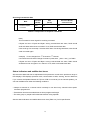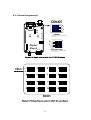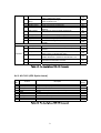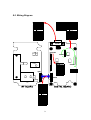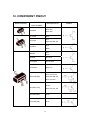
1
SD-160 Series Data Radio
(include SD-170 Series)
Technical Manual
TABLE OF CONTENTS
1. INTRODUCTION................................................................... 4
2. TECHNICAL SPECIFICATIONS ....................................... 5
3. FEATURES ............................................................................. 9
4. THEORY OF OPERATION ............................................... 23
4.1. INTRODUCTION ........................................................................... 23
4.2. DIGITAL CIRCUITS ...................................................................... 23
4.3. RF CIRCUITS................................................................................. 27
4.3.1. PLL SYNTHESIZER ................................................................................ 27
4.3.2. TRANSMITTER ....................................................................................... 28
4.3.3. RECEIVER .............................................................................................. 29
4.4. ACC-513 (GMSK MODEM CIRCUITS)........................................ 31
4.5. ACC-514 (FFSK MODEM CIRCUITS) ......................................... 32
4.6. ACC-515 (GPS INTERFACE CIRCUITS) ..................................... 33
5. MAINTENANCE AND REPAIR ........................................ 34
6. COMPONENT REPLACEMENT ...................................... 38
7. ALIGNMENT PROCEDURE ............................................. 40
7.1. RECEIVER...................................................................................... 41
7.2. TRANSMITTER .............................................................................. 42
7.3. SQUELCH ADJUSTMENT ............................................................ 43
7.4. TEST EQUIPMENT SETUP .......................................................... 45
2
8. INTERFACING .................................................................... 47
8.1. External connections ...................................................................... 47
8.2. DB-15 PIN descriptions with input/output level ............................ 47
8.3. Internal components ....................................................................... 49
8.4. Option board pin-out chart ............................................................ 50
8.4.1. ACC-513 (GMSK Modem Option board)................................................ 50
8.4.2. ACC-514 (FFSK Modem Option board) ................................................. 50
8.4.3. ACC-515 (GPS Option board) ................................................................ 51
8.5. Wiring Diagram.............................................................................. 52
9. TROUBLE SHOOTING GUIDE ........................................ 53
10. VOLTAGE CHART ........................................................... 60
11. ELECTRICAL PARTS LIST ............................................ 65
11.1. PARTS LIST FOR SD-161 ............................................................ 65
11.2. PARTS LIST FOR SD-164 ............................................................ 72
12. COMPONENT PINOUT.................................................... 79
13. SCHEMATIC DIAGRAMS............................................... 83
14. CIRCUIT B’D DETAILS................................................... 93
3
1. INTRODUCTION
The SD-160 and SD-170 Series (hereinafter called “the radios”) of RF wireless
modems from MAXON utilize the latest technology in its design and manufacturing. Both
the UHF and VHF models are Phase Lock Loop Synthesizer (PLL) / microprocessor
controlled and offer two watts (SD-160 Series) or one to five watts (SD-170 Series) of
power with 16-channel capability. Multiple functions including 1200 to 9600 baud rates,
AC and/or DC audio coupling, GMSK, FFSK and FSK modulation are standard in these
fully programmable wide bandwidth RF wireless modem units. Programmable sub-audio
squelch system (CTCSS & DCS) and two-tone squelch system are newly added to the
signal level detect squelch system (RSSI). GPS Data handling is provided to interface
and control internal GPS receiver.
The radios are programmed using an IBM® Personal Computer, DOS® or WINDOWS®
based software, an interface module and a programming cable. This allows the radio to
be tailored to meet the requirements of the individual user and of the System(s) it is
operating within.
4
2. TECHNICAL SPECIFICATIONS
GENERAL
Equipment Type :
Model Series :
VHF
UHF
Data radio (Wireless Modem)
Data radio (Wireless Modem)
SD-161
SD-171
SD-164
SD-174
Performance Specifications :
TIA/EIA-603
ETS 300-113
TIA/EIA-603
ETS 300-113
Frequency Range :
148-174MHz
148-174MHz
450-490MHz
450-490MHz
2W Only
1-5W
2W Only
1-5W
RF Output :
Channel Spacing :
12.5KHz, 25KHz Programmable
Modulation Type :
F3D, F3E
Intermediate Frequency :
45.1MHz & 455KHz
Number of Channels :
16
Frequency Source :
Synthesizer
Operation Rating :
Intermittent
90 : 5 : 5 (Standby : RX : TX)
Power Supply :
Ext. Power Supply (12 VDC Nominal)
Temperature Range :
Storage
From -40°C to +80°C
Operating
From -30°C to +60°C
Current Consumption :
Standby(Muted)
< 65mA
Transmit 5Watts RF Power
< 2.0 A
Transmit 2Watts RF Power
< 1.0 A
Lock Time :
< 10ms
TX to RX attack time :
< 20ms (No Power Saving)
RX to TX attack time :
< 20ms
Dimensions :
(32mm)H X (58mm)W X (125mm)D
Weight :
253 grams
5
TRANSMITTER
VHF
Model Series :
UHF
SD-161
SD-171
SD-164
SD-174
2W < 3W > 1.5W
5W < 6W > 4.5W
N/A
1W<1.5W>0.8W
Carrier Power : (Nom. Max. Min.)
Hi Power
Low Power
2W < 3W > 1.5W 5W < 6W > 4.5W
N/A
1W<1.5W>0.8W
Sustained Transmission :
Time : 5 10 30Sec
Power : >90% >85% >80%
Power : >90% >85% >80%
Nominal condition
< 0.5 KHz
< 0.75 KHz
Extreme condition
±5.0 ppm
±5.0 ppm
(Nominal Conditions)
Frequency Error :
Frequency Deviation :
25 KHz Channel Spacing
Peak ±5.0, Min. ±3.8
12.5 KHz Channel Spacing
Peak ±2.5, Min. ±1.9
Audio Frequency Response :
Within +1/-3dB of 6dB octave
@ 300 Hz to 2.55 kHz for 12.5 kHz C.S.
@ 300 Hz to 3.0 kHz for 25 kHz C.S.
Adjacent Channel Power :
25 KHz Channel Spacing
< 70 dBc @ Nominal Condition , < 65 dBc @ Extreme Condition
12.5 KHz Channel Spacing
< 60 dBc @ Nominal Condition , < 55 dBc @ Extreme Condition
Conducted Spurious Emission :
< -60 dBc
< -30 dBm
Modulation Sensitivity :
< -60 dBc
< -30 dBm
100mV RMS @ 60% Peak Dev.
Hum & Noise :
25 KHz Channel Spacing
> 40 dB (without PSOPH)
12.5 KHz Channel Spacing
Modulation Symmetry :
Load Stability :
> 40 dB (with PSOPH)
< 10% Peak Dev @ 1KHz input for nominal dev. + 20dB
No osc at ≥ 10:1 VSWR all phase angles and suitable antenna
No destroy at ≥ 20:1 all phase angle
Peak Deviation Range Adjustment
@ 1 KHz, Nom Dev + 20dB :
25 KHz Channel Spacing
Min. 3.5, Max. 6.0
12.5 KHz Channel Spacing
Min. 1.5, Max. 4.0
6
RECEIVER
VHF
Model Series :
Sensitivity (@ 12dB SINAD) :
25 KHz Channel Spacing
12.5 KHz Channel Spacing
Sensitivity ( 1/100 Error Rate)
With ACC-513
With ACC-514
Amplitude Characteristic :
Adjacent Channel Selectivity :
25 KHz Channel Spacing(Nom.)
(Extreme Condition)
12.5 KHz Channel Spacing(Nom.)
(Extreme Condition)
Spurious Rejection(100KHz ~ 4GHz)
Image / Half IF Rejection :
Intermodulation Response Rejection
±25 kHz/ 50 kHz
±50 kHz/ 100 kHz
Conducted Spurious Emission :
9 KHz - 1 GHz
1 GHz – 4 GHz
RX Spurious Emissions (Radiated) :
9 KHz - 1 GHz
1 GHz – 4 GHz
AF Distortion :
Nominal condition
Extreme condition
RX Hum & Noise (only audio) :
25 KHz Channel Spacing
12.5 KHz Channel Spacing
Receiver Response Time :
Squelch (factory pre-set)
Open
Close
Squelch Attack Time :
RF Level at Threshold
RF Level at Threshold + 20dB
Squelch Decay Time :
Antenna Socket Input Match
Temperature Stability for
L.O. Frequency :
L.O. Frequency Aging Rate :
UHF
SD-161
SD-171
SD-164
SD-174
< 0.28uV
< 0.30uV
< 0.28uV
< 0.30uV
< 0.28uV
< 0.30uV
< 0.28uV
< 0.30uV
< -113dBm
< -113dBm
< -110dBm
< -110dBm
> -3dB , < +3dB
< -113dBm
< -113dBm
< -110dBm
< -110dBm
> -3dB , < +3dB
> 65 dB
> 55 dB
> 55 dB
> 45 dB
> 60 dB
> 60 dB
> 70 dB
> 60 dB
> 60 dB
> 50 dB
> 70 dB
> 70 dB
> 65 dB
> 55 dB
> 55 dB
> 45 dB
> 60 dB
> 60 dB
> 70 dB
> 60 dB
> 60 dB
> 50 dB
> 70 dB
> 70 dB
> 60 dB
> 60 dB
> 70 dB
> 70 dB
> 60 dB
> 60 dB
> 70 dB
> 70 dB
< -57 dBm
< -47 dBm
< -57 dBm
< -47 dBm
< -57 dBm
< -47 dBm
< -57 dBm
< -47 dBm
< 5%
< 10%
< 3%
< 10%
< 5%
< 10%
< 40 dB without PSOPH
< 40 dB with PSOPH
< 16 ms
< 40 dB without PSOPH
< 40 dB with PSOPH
< 16 ms
-113dBm
-116dBm
< 20 ms (RSSI), < 40 ms (Analog)
< 10 ms (RSSI), < 30 ms (Analog)
5 ms Min., 20ms Max.
> 10 dB Return Loss
1st < 5 ppm, 2nd < 15 ppm from -30° to + 60° C
±2 ppm/ year
7
< 3%
< 10%
REFERENCE CRYSTAL
VHF
Model Series :
SD-161
UHF
SD-171
SD-164
Frequency :
12.8MHz
Holder Type :
HC-18
Temperature Characteristic :
SD-174
±5.0 ppm from -30° C to +60° C
< 2 ppm/ year in 1st year
Aging Rate :
< 1 ppm/ year thereafter
ENVIRONMENTAL (performance without degradation unless stated)
VHF
Model Series :
SD-161
UHF
SD-171
SD-164
SD-174
Temperature (deg C)
Operating
-30° to +60° C Degradation Specified @ Extreme condition
Storage
-40° to +80° C
ESD
20 KV
Vibration
MIL STD 810 C Procedures I, II, V and IEC68 26
Due to continuing research and development the company reserves the right to
alter these specifications without prior notice.
8
3. FEATURES
16 Channels
The SD-160 Series(include SD-170 Series, hereinafter called “SD-160”) radio can store up to 16
channels within the same band. These channels can be selected by inner DIP-S/W or serial
command inputted from external control system.
Channel Spacing
The SD-160 is capable of programmable channel spacing, in both UHF and VHF bands. Each
channel can be programmed via the PC programmer, ACC-916, having 12.5KHz or 25KHz
channel spacing.
Output Power
In case of SD-160, 2-Watts output power is only available, but, in SD-170, it’s programmable.
Each channel can be programmed via the PC programmer to a high-power output, 5 Watts, and
a low-power output, 1 Watt.
Channel Scan
For audio application, SD-160 supports channel scan enabled via serial commands. During
programming of the radio, any channel can be selected as a scanned channel. When a scanned
channel is selected, it becomes a part of the scan list. Once the scan list has been established,
initiates scan by serial commands. If a conversation is detected on any of the channels in the
scan list, the radio will stop on that channel and audio signal will be released through pin 9 of
the DB-15 connector. At that moment, busy channel data is sent to external equipment or
device through serial command. So, busy channel data can be identified as decoding received
serial command from radio in the external equipment or device. Normally, if user tries to transmit
during scanning, the transmission will be made on the channel that the call is received during
the programmable scan delay time. (The scan delay time is the amount of time the radio will
stay on that channel once working has ceased. Dealer programming of 4 ~ 7 seconds is typical).
The radio will resume scanning once the scan delay time has passed, and will continue to scan
until the serial command for scan stop is inputted by external equipment. After the scan has
resumed, if a transmission is made, the radio will transmit on the selected priority channel. This
feature is similar to priority scan TX except for selection of priority channel. You can assign a
priority channel by inner dip switch only.
9
Scan Delete
To temporarily delete a channel from the scan list, simply input the serial command for scan
deletion to the radio while scanning and stopped on the channel to be deleted. This will
temporarily remove that channel from the scan list until the scan is closed or the radio’s power is
reset.
CTCSS / DCS Scanning
To help to block out unwanted calls to your radio, the SD-160 series can be programmed by
your dealer to scan for tones.
Busy Channel Lockout
This feature, when enabled, disables the transmitter when the user would attempt to transmit
during the receiving channel is busy. It will be dealer-programmable on/off and applicable to all
channels.
Marked Idle
When used in conjunction with Busy Channel, lockouted transmitter is allowed to operate as
long as valid RX tone is received. Dealers program this feature as ON or OFF. This feature will
be dealer-programmable on/off and applicable to all channels.
TX Time-out
This feature, when enabled, limits the amount of time that the user can continuously transmit.
This time can be set in increments by 10 seconds from 10 seconds to 990 seconds. If the user
attempts to transmit longer than the TX Time-out period, five seconds prior to expiration, the
radio will release Time-out alert signal through pin 9 of the DB-15 connector and will cease
transmission.
Power Save
The function of Power Save is used when an external battery is used as the power source.
When Power Save is enabled, the receiver ON and OFF time can be programmed and allows
the operator to set the length of time the receiver gets asleep.
Tx Delay
The TX will remain active for 150 ms at the end of TX when using CTCSS tones. This eliminates
squelch tail. Dealer programs this feature as ON or OFF.
10
Squelch Options
Compared to existing Maxon data radios, programmable sub-audio squelch system (CTCSS &
DCS) and two-tone squelch system are newly added. Each channel will have these squelch
option sets during dealer programming. More detail descriptions for all available squelch
systems of SD-160 are the following.
Sub-audio squelch system
The SD-160 can operate singly or with optional modem boards. Even if user wants to use subaudio SQ system, the radio will permit this SQ option according to some cases to avoid
confliction between sub-audio and data.
Contrary to general-purpose two-way radio, the input of the radio is data or audio. In case of
audio, its frequency spectra are limited to 300㎐ ∼ 3㎑ by internal BPF. So, the division of this
and sub-audio is possible on the frequency spectra because sub-audio has under 300㎐
frequency. But, Data has wide frequency spectra compared with audio. Normally, that has 30㎐
∼ 4.8㎑ frequency (except harmonic freq.) at 9600 baud rate. Accordingly, the conflict of subaudio and data are inevitable and so broken data or SQ error is unavoidable. To solve this
problem, the radios can use the FFSK modulation which converts data into two different
continuous audio tone according to their logic levels. Therefore, available cases of sub-audio
SQ system are Audio and FFSK signal. But, it’s not permitted to FSK(FM direct modulation of
data) and GMSK signal.
a.Single operation of SD-160
If the radio operates singly, only FM direct modulation/demodulation of audio and data are
available. In this case, audio and data are inputted and released through different DB
connector lines which pin 7, 9, 1 and 2 of DB-15 connector are used as audio input, audio
output, data input and data output, respectively. Normally, Sub-audio Squelch(SQ) System
can be applied to audio signal, but data doesn’t use it to avoid frequency confliction. So, if
user tries to transmit data in one channel which has sub-audio squelch option, radio will
flash green LED two times as warning and then transmit it without sub-audio.
Note : SD-160 provides the connection of external modems to receive and transmit
external modulated data which can be inputted and outputted through pin 1 and 2
11
of DB-15 connector, respectively. In this case, the external signals are referenced
to ground and may be a.c. or d.c. coupled depending on the user requirement.
Especially, if the type of external modem is AFSK or FFSK, Sub-audio
Squelch(SQ) System can be applied by dealer programming. For reference, its
related parameter is “Tx Tone Generation for Data Input” of “Tx option” group
on the “System Option / GPS” tap window of ACC-916.
Brief block signal flow diagrams for each input are the following (See Figure 2.1. ~ 2.3.).
RF Board
Audio Amp. & Filter
Audio In
RSSI
AF
IF IC
TA31136FN
Pre-emphasis
Pre-Selector
Level
Detector
High : Audio In
Low : No Audio
Z
Y0
Y1
Y
X0
X1
X
Analog S/W
MC14053B
Mod Out
300Hz HPF
Data BPF
MF6
Sub-Audio LPF
LM386
Z0
Z1
Z
Y0
Y1
Y
X0
X1
X
Audio Out
Audio Mute
Z0
Z1
300Hz HPF
Audio Amp.
MF6
Analog S/W
MC14053B
4th Order
Sub-Audio LPF
Adj. Level
Sub-Audio LPF
Check Audio In
Tone En
Busy
MCU
Audio Mute
RSSI
MCU
Sub-Audio
Encoder
Tone Detector
MF6
Comparator
Audio signal flow in Transmitter
Audio signal flow in Receiver
Figure 3.1. Audio signal flow diagram
RF Board
AF
Level
Detector
RSSI
IF IC
TA31136FN
Data In
Audio In
High : Audio In
Low : No Audio
Mod Out
30Hz ~ 5KHz
Comparator
Data BPF
BPF
Check Audio In
Busy
Data Enable
MCU
In this case,
Sub-audio option is ignored.
RSSI
MCU
If audio input is absent,
Data path will be enabled.
Data signal flow in Transmitter
Data signal flow in Receiver
12
Data
Out
Figure 3.2. Data signal flow diagram
RF Board
Data In
Level
Detector
RSSI
AF
IF IC
TA31136FN
Pre-Selector
Audio In
High : Audio In
Low : No Audio
Z0
Z1
Z
Y0
Y1
Y
X0
X1
X
Analog S/W
MC14053B
Mod Out
Data BPF
MF6
Z0
Z1
Z
Y0
Y1
Y
X0
X1
X
BPF
MF6
Analog S/W
MC14053B
Sub-Audio LPF
Audio Out
30Hz ~
5KHz
4th Order
Sub-Audio LPF
Adj. Level
Sub-Audio LPF
Data Enable
Check Audio In
Busy
MCU
RSSI
Tone En
MCU
Sub-Audio
Encoder
Tone Detector
MF6
Comparator
Ext. Mod. signal flow in Transmitter
Ext. Mod. signal flow in Receiver
Figure 3.3. External modulated signal flow diagram
b. FFSK & GMSK
Maxon provides two optional modem boards, ACC-513, GMSK and ACC-514, FFSK for
SD-160 to improve the efficiency for data transmission and offer maximum flexibility for
user application. Selection of the required modulation option is made installing wanted
modem to radio and programming several modem parameters through PC-programmer,
ACC-916. Modem board provides the facility to connect a computerized controller via an
RS-232 level serial data interface (i.e. Communication port COM1, COM2, etc. for PCs) to
its Slave MCU. Received data from controller(DTE) will then drive the FFSK or GMSK
modulator and allow transmission of serial data. It also provides FFSK or GMSK
demodulator for the reception of FFSK or GMSK modulated data signals. These are
converted to RS-232 level serial data stream for supply to a computerized controller.
In application of Sub-audio squelch, it can’t apply to GMSK modulated signal because of
their frequency confliction. But, FFSK modulated signal can be mixed with sub-audio
because it consists of two different continuous tones which frequency spectra are on the
audio frequency region.
Brief block signal flow diagrams for each optional modem board are the following (See
Figure 2.4. and Figure 2.5.).
13
RF Board
RSSI
AF
IF IC
TA31136FN
Pre-Selector
Z0
Z1
Mod Out
Z
Data BPF
Y0
Y1
Y
Z0
Z1
X0
X1
X
Y0
Y1
Y
X0
X1
X
MF6
Analog S/W
MC14053B
Sub-Audio LPF
Z
Adj. Level
MF6
Analog S/W
MC14053B
4th Order
Sub-Audio LPF
Tone En
Sub-Audio LPF
Master MCU
Busy
Rx_En
Sub-Audio
Encoder
Tone Detector
RSSI
Tx_En
MF6
Comparator
Master MCU
Rx_En
FFSK Modem
Option Board
Tx_En
Slave MCU
Tx_CLK
Tx_Signal
(CMX469A)
TxC
Tx_Data_Out
Rx_CLK
Serial Data In
Serial Data In
FFSK Modem
Option Board
TDO
RxC
Rx_Data_In
RDI
Rx_Signal
Slave MCU
Tx_CLK
TxC
Tx_Data_Out
TDO
(CMX469A)
Rx_CLK
Rx_Data_In
FFSK signal flow in Transmitter
Serial Data Out
Serial Data Out
RxC
RDI
FFSK signal flow in Receiver
Figure 3.4. FFSK signal flow diagram
RF Board
RSSI
AF
IF IC
TA31136FN
Mod Out
Data BPF
Sub-audio option is ignored.
Master MCU
Busy
Master MCU
Rx_En
Tx_En
RSSI
Rx_En
Tx_En
GMSK Modem
Option Board
Tx_CLK
Tx_Signal
(CMX589A)
Tx_Data_Out
Rx_CLK
Rx_Data_In
Slave MCU
TxC
Serial Data In
GMSK Modem
Option Board
Serial Data In
TDO
RxC
Tx_CLK
RDI
Rx_Signal
Tx_Data_Out
(CMX589A)
Rx_CLK
Rx_Data_In
GMSK signal flow in Transmitter
Slave MCU
TxC
Serial Data Out
TDO
RxC
RDI
GMSK signal flow in Receiver
Figure 3.5. GMSK signal flow diagram
14
Serial Data Out
c. CTCSS signal information
Each channel supports the 38 TIA/EIA standard tone frequencies and 11 non-standard
tones. All tones will be set up during dealer programming.
No.
Freq.
No.
Freq.
(Hz)
No.
(Hz)
Freq.
No.
Freq.
(Hz)
No.
(Hz)
Freq.
(Hz)
01
67.0
11
97.4
21
136.5
31
192.8
41
171.3
02
71.9
12
100.0
22
141.3
32
203.5
42
177.3
03
74.4
13
103.5
23
146.2
33
210.7
43
183.5
04
77.0
14
107.2
24
151.4
34
218.1
44
189.9
05
79.7
15
110.9
25
156.7
35
225.7
45
196.6
06
82.5
16
114.8
26
162.2
36
233.6
46
199.5
07
85.4
17
118.8
27
167.9
37
241.8
47
206.5
08
88.5
18
123.0
28
173.8
38
250.3
48
229.1
09
91.5
19
127.3
29
179.9
39
69.3
49
254.1
10
94.8
20
131.8
30
186.2
40
159.8
Table 3.1. CTCSS Frequency Chart
d. DCS signal information
The radio supports the encoding and decoding of 104 DCS data (include TIA/EIA code).
Octal
Octal
Octal
Octal
Octal
Octal
Octal
Octal
Octal
Octal
Octal
Code
Code
Code
Code
Code
Code
Code
Code
Code
Code
Code
023
054
125
165
245
274
356
445
506
627
732
025
065
131
172
246
306
364
446
516
631
734
026
071
132
174
251
311
365
452
523
632
743
031
072
134
205
252
315
371
454
526
654
754
032
073
143
212
255
325
411
455
532
662
036
074
145
223
261
331
412
462
546
664
043
114
152
225
263
332
413
464
565
703
047
115
155
226
265
343
423
465
606
712
051
116
156
243
266
346
431
466
612
723
053
122
162
244
271
351
432
503
624
731
Table 3.2. DCS Code Chart
15
Two-Tone Squelch(SQ) System
The radios will support Motorola-Format, Two-Tone(Type 99) decoding. This is receive only,
decode only feature. It will allow a dispatcher to call individuals and groups. Each
System/Group will be programmable to respond to any combination of the code, with a
distinctive alert for each System/Group. The alert format consists of two tone sequences, first
the ID of the radio being called, then the ID of the calling radio.
This feature is programmed by the dealer(per customer’s request) and is not activated /
deactivated by the user. The user interface consists of the radio emitting the tones being
broadcast. At this point, the radio will enter Unmuted Rx mode and remain in this mode until the
PTT signal is inputted.
Serial command
To give the simplest protocol for control of radio, Maxon has prepared for some serial
commands which have an ease to encode and decode format. SD-160 can be used without
serial commands, but user can use its various functions through application of those, for
instance, setting-up the basic radio operation such as channel change, switch of RX/TX and
channel scan, moreover, used for control of GPS and modem option board. All messages are in
binary format, which reduces required data size to shorten response time of radio and follows
below data format.
Serial RX/TX Data Format
(1) Asynchronous Serial Data Transfer
(2) Baud Rate : 4,800 bit/sec
(3) Data Bit : 8bit , Non Parity
(4) Stop Bit : 1bit
(5) MSB first transmission
Each serial command is consist of 3 bytes. 1st byte is command and 2nd is data required by
command and 3rd is check sum to decide validity of total contents.
Byte0
ST
1st Byte (Command)
SP
2nd Byte (Data)
SP
3rd Byte (Check Sum)
SP
Byte1
ST
Byte2
ST
16
Data Protocol
a. Protocol for input serial command
Protocol of data transmission from external equipment or device (: PC) to radio :
External equipment or device
Radio
Input serial command
Response
Receive response
Figure 3.6. Protocol for input serial command
b. Protocol for output data
Protocol of data transmission from radio to external equipment or device (: PC) :
External equipment or device
Radio
Output Data
(with command)
Receive Data
Output Data
(with command)
Receive Data
Figure 3.7. Protocol for output data
Detail information of Serial Commands
a. Transmitting Command & Data
Mode
Command
Data
Check sum ( BYTE2 )
(BYTE0)
( BYTE1 )
: Command + Data
17
1.
2.
Channel Change
RTX Mode Selection
3.
From PC
0x64
0x?? :Current channel
( 0x64 + Channel )
0x61
R(0x72) : Rx mode
( 0x61+0x72 )
T(0x74) : TX mode
( 0x61+ 0x74 )
F(0x46) : Scan Stop
( 0x62+ 0x46 )
S(0x73) : Scan Start
( 0x62+ 0x73 )
O(0x4F) : Scan Delete
( 0x62+ 0x4F )
0x00 : 1 Channel
0x66 + 0x00
0x01 : 2 Channel
0x66 + 0x01
0x02 : 3 Channel
M
0x62
To Radio
0x66
From Radio
To Pc
*Only for Unmute Channel,
M
Scan Mode
0x0f : 16 Channel
0x65
Correct Call Channel
It occurs when Scan Delete command comes except
Busy/Correct Call
Error
It occurs when PTT key is pushed except
Message
Busy/Correct Call.
It occurs when channel change command exists
during Scanning.
4.
Control of
0x6a
GPS Power
0x63
GPS
mode
Control of
0x00 : GPS Power Off
( 0x6a + 0x00 )
0x01 : GPS Power On
( 0x6a + 0x01 )
0x00 : GPS Data Disable
( 0x63 + 0x00 )
0x01 : Release GPS Data
( 0x63 + 0x01 )
to DB-15
GPS Data
0x02 : Release GPS Data
( 0x63 + 0x02 )
to Modem
5.
Modem test mode
6.
GMSK
0x75
0x7a
Modem
0x7c
alignment
mode
FFSK
0x7e
0x78 : Enable test data
( 0x75 + 0x78 )
0x79 : Disable test data
( 0x75 + 0x79 )
0x00 : Disable
( 0x7a + 0x00 )
0x01 : Enable
( 0x7a + 0x01 )
0x00 : Disable
( 0x7c + 0x00 )
0x01 : Enable Mark data
( 0x7c + 0x01 )
0x00 : Disable
( 0x7e + 0x00 )
0x01 : Enable Space data
( 0x7e + 0x01 )
Table 3.3. Composition of input serial commands
18
Receiving Command & Data
Mode
1
Command
Data
Check sum (BYTE2)
(BYTE0)
(BYTE1)
: Command + Data
Process Complete
0xaa
ACK
N/A
Commands
0x55
NACK
N/A
Table 3.4. Composition of response commands
Note)
This command is return signal for receiving command.
If Byte2 and sum of Byte0 and Byte1 among received data are same, Radio would
send ACK data and execute command. If not, Radio sends Nack data.
User would go into next step if receives ACK data. If receiving Nack data, user should
send command again.
example) If user changes from 1st Channel to 2nd Channel,
user should send Channel Change Command ( 0x64,0x02 , ( 0x64 + 0x2 ) ) to Radio.
If Byte2 and sum of Byte0 and Byte1 among received data are same, Radio sends
ACK data to user and goes to 2nd channel. If not, radio would send Nack data.
Status indicators and audible alert tones
SD-160 series data radio has a sophisticated microprocessor control which provides a range of
LED displays. LED displays operation mode, current status of radio, warning, and etc. Moreover,
if you connect the Speaker filtered OUT (Pin 9 of DB-15 connector) to an external speaker, you
can hear audible tones under the following conditions:
• Attempt to transmit on a channel which is already in use when busy channel lockout option
has been programmed
• Transmission time has exceeded time-out timer programmed length
• The other group or people has finished transmission using repeater
See the status indicators and audible alert tones chart (Table 2.5.) for full specification.
19
STATUS
NORMAL
DESCRIPTION
LED COLOR
POWER ON
-
Busy Channel
Yellow
Correct Call
Green
Transmit
Yellow
AUDIBLE TONE
Transmit Not Allowed
SCANNING
WARNING
Normal Scan Mode
Green LED Flash
Scan Delete
one time Red LED
Scan All Delete
Two times Red LED
Busy Channel lockout
two times Green LED
Time out Time
one time Green LED
Before 5S T-O-T
one time Green LED
EEPROM Error
one time Yellow LED
Unlock
Four times Yellow LED
Single Beep Tone
Single Beep Tone
Communication error with Modem Green LED flash
MCU
Transmit Hang on time
-
Single Beep Tone
Under channel programmed sub- Two times Green LED
audio SQ, when transmission is
tried by input of FSK or GMSK
data.
PROGRAM
Read Mode
Red LED flash
Write Mode
Green LED flash
AUTO TEST
Yellow
Open Squelch Mode
three times Green LED
SQUELCH
Close Squelch Mode
Two times Green LED
PROGRAM MODE
Save Squelch Mode
One time Green LED
Init Data Load
one time Green LED
Table 3.5. status indicators and audible alert tones
20
Modem Option for data communication
ACC-513 and ACC-514 are new kinds of internal option-modems, which are applied to SD-160
series to increase capability for data application. The goal of internal modem is to improve the
efficiency for data transmission and provide maximum flexibility for user application. In former
case, the most obvious method of increasing the efficiency is to maximize the data signaling
speed in the limited channel bandwidth. But, FSK, called direct FM modulation, has very wide
transmission bandwidth requirement. To solve this problem, Maxon supplies GMSK(Gaussian
Filtered Minimum Shift Keying) internal option-board. In latter case, to improve quality of service,
some of service provider (or user) want to apply new radio to their existing system without
additional investment to establish new system even if it’s audio system. But, data application
can’t be directly applied in audio system because of its spectra characteristic. Generally, spectra
of data have wider bandwidth than audio. So, direct application of data is not matched with
audio system and its application. For instance, if sub-audio(Tone) SQ system is applied to data
application, its frequency spectra conflict with that of sub-audio. Moreover, if inputted data is
filtered by audio filter circuit to avoid this problem, some of that will be broken. Therefore, to get
over these problems and provide maximum flexibility, Maxon prepares FFSK(Fast Frequency
Shift Keying) internal option-board.
Our internal modem option boards consist of Slave MCU, Modem IC, and extra circuitry. These
option-boards directly communicate with DTE (Data Terminal Equipment) to send and receive
the meaningful data through the DB-15 connector on digital board of SD-160. These are
designed to accept RS232 serial data format and also capable of high speed wireless datatransmission between two or more devices. More detail information for modem option boards is
given in technical manual for ACC-513/514. Moreover, dealer will help you define a TX On/Off
Delay time, RX On Delay time, Baud Rate, Modem Enabled, Modem Baud Rate, Data flow
control, and Test Mode.
Table for modem speed
Channel Space
Narrow (12.5KHz)
Standard (25KHz)
DTE Baud Rate
Modem Baud Rate
1200
1200
2400
2400
1200
1200
2400
2400
4800
4800
Table 3.6. Available Baud rate for FFSK modem
21
Channel Space
DTE Baud Rate
Modem Baud Rate
Narrow (12.5KHz)
4800
4800
4800
4800
9600
9600
Standard (25KHz)
Table 3.7. Available Baud rate for GMSK modem
GPS option board
As one of methods to satisfy various requests for user application, SD-160 basically supports
GPS data handling. That may help your implementation for system related to GPS.
Nevertheless, if it’s not enough for each your application, received position data from GPS
module placed in SD-160 can be reprocessed by your own application. ACC-515 is GPS
module for SD-160, which releases some of 11 different output data according to NMEA-0183
format. Moreover, it can be also selected by user, but it should be processed by user’s
application. Received data from ACC-515 will be released via DB-15 connector of SD-160
or/and transmitted to other system through installed modem. More detailed information for GPS
option board is given in technical manual for ACC-515.
22
4. THEORY OF OPERATION
4.1. INTRODUCTION
The VHF and UHF radios comprise of two PCBs (RF and digital PCB). These boards are
connected by an 18 pin female and male connector. The digital board which controls the radio
and data receiving and sending is interfaced with external data equipment through the 15 pin dsub female (DB-15) connector.
4.2. DIGITAL CIRCUITS
The Digital circuit contains the CPU, the channel select switch, and associated digital circuits.
TX-SIGNAL CIRCUIT
There are two signal paths in the Tx-signal circuit. One is FSK data signal path and the other is
the audio signal path. The FSK data signal from Pin 1 of DB-15 connector (CON401) goes
through IC406-C. The signal is amplified by IC404-C and then its amplitude is limited by IC404D. After that, this signal is filtered by an 8’th order low pass filter (IC405) in order to reduce the
required transmission bandwidth. The first two stages of
the 8’th order LPF consist of
a
Gaussian filter for the improvement of ramp function response and the last two stages use a
Butterworth filter for attenuation. The output of the LPF is then fed to the RF board for TX
modulation.
Audio signal, from Pin 7 of DB-15 connector is fed into the 300Hz High pass filter(IC408)
through the IC406-B and IC409. The HPF removes sub-audible voice products for application of
Sub-audio(Tone) squelch system (CTCSS, DCS) and then the output from IC408 is fed into
IC404-A&B with associated parts to form a mic amplifier and pre-emphasis circuit. After that, the
pre-emphasized Tx-audio signal is inputted to the RF board for Tx modulation through the FSK
data signal path.
RX-SIGNAL CIRCUIT
The Rx-signal circuit also has two signal paths. One is the data signal path and the other is the
audio signal path. The Rx signal comes from the RF board, which is connected with pin 10 of
CON405. Data signals are switched in IC406-D by a Busy signal which is activated when the
radio receives a valid RF signal, and is filtered by IC416-A and then its amplitude level is
23
adjusted (amplified) by IC416-B. The amplitude-adjusted signal goes to pin 2 of the DB-15
connector (CON401).
Audio signals are inputted to the 300Hz High pass filter (IC408) to eliminate sub-audible voice
products through IC409. The output of the HPF is switched by IC406-A and de-emphasized by
resister R471 and C452. After that, its level is adjusted by RV401 and then that is amplified by
IC412 (LM386 : Audio amplifier). The amplified signal goes to pin 9 of CON401 (DB-15).
ANALOG SWITCH
IC409 (MC14053B) is a digitally controlled analog switch which internally consists of three
single pole, double throw switches. By placing a high (5V) or low (0V) on the control lines which
consists of A, B and C. A controls the X ports, B controls the Y ports and C controls the Z ports.
Example: A high on control A would connect X to X1. A low on control A would connect X to X0.
HIGH PASS FILTER
The 300Hz high pass filter is an 8-pole 1dB Chebeyshev active filter that comprises of IC410
and associated components. Received audio is passed to IC408 from Pin 4 of IC409 where
sub-audible tones below 300Hz are removed. Tx (Mic) audio is also fed into IC408 via IC 409
(Pin 4) where sub-audible voice products below 300Hz are also removed.
CTCSS/DCS DECODE CIRCUITS
Discriminated audio from Pin 9 of IC6 is fed into IC411-B and associated parts which are the
first 2 poles are part of a 6th order 250 Hz Chebeyshev low pass filter. The output from pin 1
(IC411-B) is fed into IC409 (Pin 2) and outputs to pin 15 (IC409). The signal is then fed to Pin 8
(IC410) which is a 6th order low pass Butterworth switched capacitor filter. The output from the
Butterworth filter (Pin 3 of IC410) is then fed to the remaining second 4 poles part of the 6th
order Chebeyshev filter, which consist of IC411-D and one of the two internal operational
amplifiers of IC410 (MSNBLPS) along with associated components. Both the Chebeyshev and
the Butterworth combines for a 4dB ripple low pass filter when programmed for 250 Hz. The
output of IC411-D (Pin 14) is fed into the remaining internal operational amplifier of IC410
(MSNBLPS) which forms the squaring circuit for the signal decode. The signal is out from Pin 2
of IC411 (MSNBLPS) and fed into IC401 (MCU) where it is compared whether that is matched
with preprogrammed data or not. If matched, valid data is decoded, shown by a green L.E.D.
on the top panel of the radio, and audio is released through pin 9 of DB-15 Connector. If
24
unmatched, the busy L.E.D. (Yellow) would be shown.
CTCSS/DCS ENCODE CIRCUITS
During TX encode, the tone squelch digital signal is produced as a 3-bit parallel word at Pins 33,
34, and 35 of the micro controller (IC401). The 3-bit digital signal is converted to an analog
signal by resistors R481, 482 and 483. The analog signal is fed into Pin 1of IC409 and out on
Pin 15 (IC409) and then fed into Pin 8 of IC410 (6th order Butterworth clock tuned low pass
filter). The filtered encode output from Pin 3 (IC410) is fed to IC411-A and RV402 (sub-audible
gain control), the output of IC411-A is then fed to the audio mixer circuit of the RF board.
TWO TONE DECODE CIRCUITS
Two tone uses frequency with audio. Discriminated audio from the RF board is inputted to the
comparator (two tone decoder : IC403-B) which forms the squaring circuit for the decode signal.
The signal is output from Pin 7 of IC403-B and fed into IC401 (MCU) where it is compared
whether it is matched with preprogrammed data or not. If matched valid data is decoded, which
is shown by a green L.E.D. on the top panel of the radio and audio is released through pin 9 of
the DB-15 Connector. If unmatched, the busy L.E.D. (Yellow) is shown.
RSSI DETECTOR
From the RF board, the RSSI (Received Signal Strength Indicator) signal flows to Pin 31 of
IC401(MCU) through R513. Micro controller unit (IC401) detects received signal level using the
inner 8-bit ADC(Analog to Digital Converter). The output of ADC is compared with the
programmed RSSI level. If the MCU detects existence of a received signal through these
comparison a yellow L.E.D. is shown on the top panel of the radio.
EEPROM
RX / TX channel and RSSI detection level as well as other data from the programmer are stored
in the EEPROM. The stored data is retained without power supply. This is a non-volatile
memory and re-programmable. IC402 is an EEPROM with 4096 (8 x 512) capacity and data is
written and read serially.
25
CHANNEL SELECTOR
One of 16 channels may be selected using the Dip Switch (SW401) and serial commands. The
hardware selector, SW401 encodes the channel number, selected into 4-bit binary code. The
binary code plus one equals the channel number. The binary code is decoded by the CPU,
which enables the appropriate RX or TX frequency and associated data to be selected from the
EEPROM. External serial commands which come from Pin 8 of the DB-15 Connector (CON401)
are fed into Pin 41 of IC401 (MCU). The micro controller uses UART (Universal asynchronous
receiver transceiver) for serial communication and decodes serial commands in order to control
the radio.
DC TO DC CONVERTER
The main DC power is supplied to the switched mode DC to DC converter . The DC to DC
converter regulates the various input power supply voltage and outputs a constant voltage of
6.5 Volts (SD-161, SD-164) or 7.5 Volts (SD-171, SD-174). It is a source for all of the RF and
digital circuits. The DC to DC converter is formed by IC801, Q801, Q802, L801, R804 and
voltage divider(R805, R806, R802). IC801 is a PWM controller that controls pulse width of the
switching pulse output. Various input voltage appears as various output voltage of voltage
divider. IC801 detects the voltage difference between inner reference voltage and the voltage
divider output controls the switching pulse width in proportion to its difference. Wanted output
voltage is decided by product of input voltage and duty ratio of switching pulse. As the switching
pulses, Q801and Q802 switch the input DC of various supply voltages and generate the
constant DC of supply voltage. IC801 controls maximum current of DC to DC converter by
current detection through voltage drop of R804.
26
4.3. RF CIRCUITS
4.3.1. PLL SYNTHESIZER
12.8 MHz TCXO
The TCXO contains the 3-stage thermistor network compensation and crystal oscillator and
modulation ports. Its compensation is ±5 PPM or less from -30c to +60c.
PLL IC DUAL MODULE PRESCALER
Input frequency of 12.8 MHz to pin 1 of IC2 MB15A02 (or MB15E03SL) is divided into 6.25 kHz
or 5 kHz by the reference counter and then supplied to the comparator. RF signal input from the
VCO is divided to 1/64 at the 64/65 modulus prescaler in IC2, divided by A and N counter in IC2
to determine frequency steps, and then supplied to the comparator. PLL comparison frequency
is 6.25/5 kHz, so its minimum programmable frequency step is 6.25/5 kHz. The A and N counter
is programmed to obtain the desired frequency by serial data in the CPU. In the comparator, the
phase difference between reference and VCO signal is compared. When the phase of the
reference frequency is leading, ΦP is the output, but when the VCO frequency is leading, ΦR is
the output. When ΦP= ΦR, phase detector out is a very small pulse.
EXTERNAL CHARGE PUMP
This is used to increase dynamic range of VCO. Voltage range is decided by the supply voltage
of the charge pump and the DC to DC converter which supplies that voltage. 0-12v is necessary
for controlling the VCO. In addition the radio adopts a current mode charge pump to take direct
control of such parameters as charge pump voltage swing, current magnitude, TRI-STATE
leakage, and temperature compensation. ΦP, ΦR logic signals are converted into current
pulses to enable either charging or discharging of the loop filter components to control the
output frequency of the PLL.
REFERENCE FREQUENCY LPF
The Loop Filter contains R9, C1 and C2. LPF settling time is 12mS with 1 kHz frequency. This
also reduces the residual side-band noise for the best signal-to-noise ratio.
27
DC TO DC CONVERTER
The DC to DC converter converts 5v to 14-16v to supply the necessary voltage for wide range
frequency in the VCO.
VCO
The radio adopts a two VCO system for RX and TX in order to maximize each performance.
The TX and RX VCO generates RF carrier and local frequency and each VCO is switched by a
TX/RX power source. It is configured as a Colpitts oscillator and connected to the buffer as a
cascade, the bias circuit is a cascade configuration to save power. The varicap diode
D201/D301are low-resistance elements and have different capacitance for reverse bias voltage.
Using the change of reverse bias voltage (2 ~ 11V), the wanted frequency for each channel can
be obtained. L203/L303 are resonant coils and C208/C308 are used to change the control
voltage by the tuning core. D202 modulation diode modulates the audio signal. C204
compensates the non-linearity of the VCO due to the modulation diode and maintains a
constant modulation regardless of frequency.
4.3.2. TRANSMITTER
The transmitter consists of:
1. Buffer
2. P.A. Module
3. Low Pass Filter
4. Antenna Switch
5. A.C.C. Circuits
BUFFER
VCO output level is -4dBm and amplified to +10dBm. The buffer consists of Q9 and Q10 for
reverse isolation and gain.
P.A. BLOCK
The P.A. Block uses a three stage amplifier and contains Q501, Q502, and Q503. The SD-171,
SD-174 have different amplifiers applied compared to the SD-161, SD-164 because different of
a output power specification. Q501 amplifies the TX signal from +10 dBm to 100mW and Q502
28
amplifies to 0.5W and Q503 amplifies to 3W(SD-161, SD-164) or 6W(SD-171, SD-174) and
then matched to 50 Ohms using the L.C. network or strip line, thereby reducing the harmonics
by -30 dB.
LOW PASS FILTER
L7, L8, L9, C36, C37, C38 and C39 are the 7th order Chebyshev low pass filter. Unwanted
harmonics are reduced by -70 dBc.
ANTENNA SWITCH
When transmitting, the diodes D3 and D5 are forward biased to enable to make an RF path to
the antenna. D5 is shorted to ground to block the RF signal to the front-end. In receive, the
diodes, D3 and D5, are reverse biased to pass the signal from the antenna through L10 and
C61 to the front-end without signal loss.
AUTOMATIC CURRENT CONTROL (ACC) CIRCUITS
The ACC circuit consists of R63, variable resistor RV4, IC5(B) and transistors Q11 and Q12.
The supplied current to the P.A. block is monitored by the voltage difference on R63 (0.1 Ohm).
If the current varies by RF power output or other reasons, it produces a voltage difference on
R63 and then IC5A outputs a bias voltage to Q19 in proportion to that difference. The adjusted
value of Q15 output by RV4 is compared with the reference voltage in IC5B and then a
differential voltage at the output of IC5B is passed to Q12 and Q11 which controls the bias
voltage of the P.A. module to maintain a constant power output to the antenna. RV4 is used to
adjust the RF power level.
4.3.3. RECEIVER
FRONT-END
The front-end block consist of two band pass filters and a low noise amplifier (LNA). The Band
pass filter is used for elimination of image frequency and impedance matching and the LNA is
used to amplify weak RF signals without any increase of noise. The received signal comes from
the antenna, then is input into a band pass filter of the front-end block with C601through C610,
L601 through L604 at UHF and C622 through C608, L607 through L604 at VHF, and is coupled
29
to the base of Q601 serving as an RF amplifier. Diode D601 serves as protection from static RF
overload from nearby transmitters. The output of Q601 is then coupled to a second band pass
filter consisting of C611 through C623 and L606 through L609 at UHF and C607 through C601,
L603 through L601 at VHF. The output of the front-end block is then coupled to the double
balanced diode mixer D6. The Front-end block is pre-tuned at factory and no more adjustment
is required
FIRST MIXER
The Double balanced diode mixer consists of D9, T1 and T2 and generates the 45.1 MHz
intermediate frequency output from RF and local frequency. The filtered frequency from the
front-end module is coupled to T1and the local frequency from RX VCO is coupled to T2. The
45.1 MHz IF output is matched with the input of the 2-pole monolithic filter by L12, L13, C65 and
C66. The crystal filter provides a bandwidth of ±7.5 kHz at the operating frequency for a high
degree of spurious and inter-modulation protection. The IF filter provides additional attenuation
for the image frequency of the second mixer. The output impedance of the filter is matched with
the base of the post amplifier Q16 by C67 and C70.
SECOND OSCILLATOR MIXER LIMITER AND FM DETECTOR
The output of the post amplifier, Q16, is coupled via C71 to the input of IC6 (TA31136FN). IC6
is a monolithic single conversion FM transceiver, containing a mixer, the second local oscillator,
limiter and quadrature detector. Crystal X1, 44.645 MHz, is used to provide resultant 455kHz
signal from the output of the second mixer. The mixer output is then routed to CF1 (455F) or
CF2(455HT). These ceramic filters provide the adjacent channel selectivity of 25 kHz or 12.5
kHz bandwidth. After that, filtered signal is fed to the limiter and then audio is derived from the
limited signal at the quadrature detector.
RSSI ( RECEIVER SIGNAL STRENGTH INDICATOR )
The RSSI signal is output from IC6 on pin 12. The output is an analog DC voltage and varied as
much as the received signal strength. The signal which is filtered unwanted noise by the low
pass filter (IC4-B) in the RSSI signal is used for squelch system. Also, this signal is
compensated with a thermistor (TH3) at temperature.
30
4.4. ACC-513 (GMSK MODEM CIRCUITS)
MAXON GMSK option modem boards uses a CMX589A IC to generate and decode GMSK
signals. The modem fully supports auto mode, dump mode (RTS mode) and extended dump
mode operation. This section describes only the operation of circuit. A special characteristic of
GMSK modems is that they can use a high data throughput in limited channel space.
TX-SIGNAL CIRCUIT
The transmit data (TXD) signal from Pin 1 of CON2 is level-shifted to TTL levels by Q1 and then
applied to the Pin 45(UART port) of U1 (slave MCU). The slave micro controller stores received
data in the memory buffer and releases stored data to U2 (CMX589A) by the transmit clock
pulses of the CMX569A. Random timed asynchronous input from the external data terminal is
synchronized by the MCU and then synchronous information is sent into U2 (CMX589A), which
filters the data stream through a Gaussian filter in order to reduce transmission bandwidth. The
cut-off frequency of the Gaussian filter is decided by a transmit bit ratio. Output signal of the
GMSK modem is fed into a RC network formed by R12 and C10 that is positioned to reduce
high-frequency noise. To adjust the cut-off frequency of the RC network, R22and U6, is used.
The filtered signal is inputted to the gain amplifier and the 3rd order low pass filter (U5) through
a buffer. The first stage of U5 is used as a buffer and the second stage is a gain amplifier to
supply sufficient amplitude level for modulation and the third stage comprises of an additional
3rd order Butterworth LPF to guarantee maximum attenuation of high-frequency noise before
modulation. The output of the LPF is then fed to the RF board for TX modulation.
RX-SIGNAL CIRCUIT
Discriminated signal from the RF board is amplified by IC416-C in the digital board to have a
proper level for data detection. The amplified signal is fed into the GMSK modem option board
and then inputted to Pin 11 of U2(CMX589A) through Pin 14 of CON1. The CMX589A detects
synchronous data and recovers receive clock and then each data and clock is sent into U1
(slave MCU) for conversion back into asynchronous data. This information is then sent out to
the data terminal through the U3 (MAX234).
LEVEL CONVERTER
The MAX234 level converter (U3) and peripheral circuitry with Q1, Q2 convert TTL input/output
levels to the nominal +/- 10V, RS-232 input/output levels. If dump or extended dump mode is
used an additional handshake
signal is required. The PTT, Carrier Detect and Busy signal
are used as handshake signals. The PTT signal level is shifted from RS-232 to TTL level and
Carrier Detect and Busy signal is shifted from TTL to RS-232 level.
31
4.5. ACC-514 (FFSK MODEM CIRCUITS)
MAXON FFSK option modem boards uses a CMX469 IC to generate and decode FFSK signals.
The modem fully supports auto mode, dump mode (RTS mode) and extended dump mode
operation. This section describes only the operation of the circuit. A special characteristic of
FFSK modems is that they can apply the sub-audio (tone) squelch system (CTCSS, DCS) to
data communication.
TX-SIGNAL CIRCUIT
The transmit data (TXD) signal comes from Pin 1 of CON2 that is level shifted to the TTL levels
by Q1 and then it’s applied to the Pin 45(UART port) of U1 (slave MCU). The slave micro
controller unit stores received data in the memory buffer and releases stored data to U2
(CMX469A) by transmit clock pulses of the CMX469A. Random timed asynchronous input from
the external data terminal is synchronized by the MCU and synchronous information is sent to
U2 (CMX469A), which converts the logic 0 and 1 into a sine-wave signal with two different
frequencies. At this moment, frequency is decided by a transmit bit ratio. The converted signal
is fed into a gain amplifier and 5th order low pass filter (U5). The first stage of U5 is used as a
gain amplifier to supply sufficient amplitude level for modulation and the next two stages
comprise of a 5th order Butterworth LPF to guarantee maximum attenuation of high-frequency
noise before the modulation. The output of the LPF is then fed to the RF board for TX
modulation.
RX-SIGNAL CIRCUIT
Discriminated signal from the RF board is amplified by IC416-C in the digital board to have
proper level for data detection. The amplified signal is fed into the FFSK modem option board
and then inputted to Pin 16 of U2(CMX469A) through Pin 14 of CON1. The CMX469A detects
synchronous data and recovers receive clock and then each data and clock is sent into U1
(slave MCU) for conversion back into asynchronous data. This information is then sent out to
the data terminal through U3 (MAX234).
LEVEL CONVERTER
The MAX234 level converter (U3) and peripheral circuitry with Q1, Q2 convert TTL input/output
levels to the nominal +/- 10V,RS-232 input/output levels. If dump or extended dump mode is
used an additional handshake signal is required. PTT, Carrier Detect and Busy signal are used
as handshake signals. The PTT signal level is shifted from RS-232 to TTL level and Carrier
Detect and Busy signal are shifted from TTL to RS-232 level.
32
4.6. ACC-515 (GPS INTERFACE CIRCUITS)
The radio series outputs an industry standard NMEA GPS sentence on the DB-15 connector
when the GPS option board is installed. The GPS module releases NMEA-0183 format data
every 1sec. To prevent unnecessary data from the GPS engine, the GPS output is controlled by
Pin 6 of J1 (GPS_OUT), and besides, power save mode can be executed by Pin 4 of J1
(PSAVE). Even if GPS engine enters power save mode, Back-up voltage should be supplied to
Pin 3 of J3 (B+) in order to use warm start at wake-up. The GPS option board and GPS antenna
require a different supply voltage level compared with the main supply voltage of the radio. The
GPS interface circuit supplies a regulated 3.3V power to the GPS board.
33
5. MAINTENANCE AND REPAIR
GENERAL
Any repair or adjustment should only be made by or under the supervision of a qualified radio
service technician. When removing or fitting, use the Exploded View and Parts List in
conjunction with the following procedures:
Important: Before disassembling and reassembling the radio, wear a conduction wrist strap to prevent
any components on its main board from being damaged by electrostatic discharge.
SEPARATING UPPER AND BOTTOM COVER
1. Unfasten the four mounting screws
located on the bottom cover of
the radio.
Figure 5.1. Loosing the four mounting screws
2. Open slowly the upper cover from the side of
power connector.
Fig 5.2. Opening the upper cover
34
3. Separate upper cover from bottom
cover by removing RF cable of ANT.
connector.
Fig 5.3. Separating upper and bottom cover
REMOVING & REPLACING THE RF BOARD
1. Unscrew the four upholding screws from
the RF board.
2. Remove the shield plate.
Fig 5.4. Removing shield plate
35
3. Unscrew the two mounting screws located
on shield can for PA module.
4. Replace the RF board assembly.
Fig 5.5. Replacing RF board assembly
REMOVING & REPLACING THE DIGITAL BOARD
1. Unfasten the two hexagonal screws from
DB-15 connector.
2. Loosen the mounting screw located on
the left side of digital board
3. Remove two wires between power
connector and digital board.
Fig 5.6. Removing screws and wires from digital B’D
36
4. Pull the digital board out of bottom cover.
5. Replace the digital board assembly.
Fig 5.7. Replacing digital board assembly
37
6. COMPONENT REPLACEMENT
Surface Mount Components
Surface mount components should always be replaced using a temperature controlled soldering
system. The soldering tools may be either a temperature controlled soldering iron or a
temperature controlled hot-air soldering station. A hot-air system is recommended for the
removal of components on these boards. With either soldering system, a temperature of 700° F
(371° C) should be maintained. The following procedures outline the removal and replacement
of surface mount components. If a hot-air soldering system is employed, see the manufacturer’s
operating instructions for detailed information on the use of your system.
CAUTION: Avoid applying heat to the body of any surface mount component using
standard soldering methods. Heat should be applied only to the metalized terminals of the
components. Hot-air systems do not damage the components since the heat is quickly and
evenly distributed to the external surface of the component.
CAUTION: The CMOS Integrated Circuit devices used in this equipment can be destroyed
by static discharges. Before handling one of these devices, service technicians should
discharge themselves by touching the case of a bench test instrument that has a 3-prong
power cord connected to an outlet with a known good earth ground. When soldering or
desoldering a CMOS device, the soldering equipment should have a known good earth
ground.
Surface Mount Removal
1. Grip the component with tweezers or small needle nose pliers.
2. Alternately heat the metalized terminal ends of the surface mount component with the
soldering iron. If a hot-air system is used, direct the heat to the terminals of the component.
Use extreme care with the soldering equipment to prevent damage to the printed circuit board
(PCB) and the surrounding components.
3. When the solder on all terminals is liquefied, gently remove the component. Excessive force
may cause the PCB pads to separate from the board if all solder is not completely liquefied.
4. It may be necessary to remove excess solder using a vacuum de-soldering tool or Solder
wick. Again, use great care when de-soldering or soldering on the printed circuit boards. It
may also be necessary to remove the epoxy adhesive that was under the surface mount
component and any flux on the printed circuit board.
38
Surface Mount Component Replacement
1. “Tin” one terminal end of the new component and the corresponding pad of the PCB. Use as
little solder as possible.
2. Place the component on the PCB pads, observing proper polarity for capacitors, diodes,
transistors, etc.
3. Simultaneously touch the “tinned” terminal end and the “tinned” pad with the soldering iron.
Slightly press the component down on the board as the solder liquefies. Solder all terminals,
allowing the component time to cool between each application of heat. Do not apply heat for
an excessive length of time and do not use excessive solder. With a hot-air system, apply hot
air until all “tinned” areas are melted and the component is seated in place. It may be
necessary to slightly press the component down on the board. Touch up the soldered
connections with a standard soldering iron if needed. Do not use excessive solder.
CAUTION: Some chemicals may damage the internal and external plastic parts of the radio.
4. Allow the component and the board to cool and then remove all flux from the area using
alcohol or another approved flux remover.
Surface Mounted Integrated Circuit Replacement
Soldering and de-soldering techniques of the surface mounted IC’s are similar to the above
outlined procedures for the surface mounted chip components. Use extreme care and observe
static precautions when removing or replacing the defective (or suspect) IC’s. This will prevent
any damage to the printed circuit board or the surrounding circuitry.
Note: The hot-air soldering system is the best method of replacing surface mount IC’s. The
IC’s can easily be removed and installed using the hot-air system. See the manufacturer’s
instructions for complete details on tip selection and other operating instructions unique to
your system. If a hot-air system is not available, the service technician may wish to clip the
pins near the body of the defective IC and remove it. The pins can then be removed from
the PCB with a standard soldering iron and tweezers, and the new IC installed following the
Surface Mount Component Replacement procedures. It may not be necessary to “tin” all (or
any) of the IC pins before the installation process.
39
7. ALIGNMENT PROCEDURE
The UHF/VHF Transceivers have broadband tuning range, UHF (450-490 MHz) and VHF (148174 MHz) should require no special alignment, unless repairs are performed on the transceiver
portion. Should repairs be necessary, use the "Test Equipment Diagram" and the “Alignment
Points Diagram", in conjunction with the following procedures:
Extender Board (ACC-516) is required in order to separate the Digital and RF PCB’s to
allow access to the alignment points. Installation instructions are provided with the
Extender Board Assembly.
Outpt Audio level
SQ for S-BAND
CON407
RV5 RV6
RV401
SQ for N-BAND
Low
Power
RV4
RV3
RV402
TCXO1
Tone Deviation
High
Power
Tx
VCO
frequency
Rx
VCO
C208
RV403
Ref. level for
Modem
SW401
Balence
C308
RV1
RV2
TP1
Deviation
RF BOARD
DIGITAL BOARD
Figure 7.1. Alignment Points Diagram
40
7.1. RECEIVER
RX VCO
RX VCO is pre-tuned at the factory and adjustment should not be required
To identify existence of defect of RX VCO, check the VCO Control voltage.
1. Set the unit to the highest receive frequency, 490MHz(UHF2), 174MHz(VHF) and verify
the VCO control voltage is under 10.0 Volts. If it’s over 10.0 Volts, adjust C308 of RX
VCO to 10.0 Volts
2. Set the unit to the lowest receive frequency 450MHz(UHF2), 148(VHF) and verify that
the VCO voltage is above 2.0 Volts. Adjust C308 to 2.0 Volts.
※ Note: Use TP1 to measure the voltage.
AUDIO OUTPUT LEVEL Adjustment
1. Select a receiver channel that is programmed for Standard band (25kHz) operation.
2. Prepare standard test signal as follows.
a. Set the RF signal generator to the receiver frequency.
b. And then set the AF modulation signal to 1 kHz at 3kH deviation.
c. Adjust the RF output level of the RF signal generator to –47dBm.
3. Apply a standard test signal to the receiver antenna terminals.
4. Adjust RV401 for the specific audio output level.
LEVEL SHIFTER for Modem option Board (ACC-513, ACC-514)
1. Select a receiver channel which is programmed for Standard band (25kHz) operation.
2. After Preparing standard test signal for Standard band, apply that signal to the antenna
terminals of receiver.
3. Adjust RV403 until the center voltage of demodulated signal (1KHz sine wave) of TP401 is
2.5 Volts.
4. Select a receiver channel which is programmed for Narrow band (12.5kHz) operation.
5. After Preparing standard test signal for Narrow band (only decrease deviation of AF
modulation signal as 1.5K from standard test signal for Standard band), apply that signal to
the antenna terminals of receiver.
6. Verify the center voltage of demodulated signal of TP401 is 2.5 Volts. If different, Adjust
RV403 until the center voltage is near 2.5 Volts for each band (25KHz / 12.5KHz).
41
7.2. TRANSMITTER
Connect the unit to a Service Monitor with the power meter set to the 10 W scale (or autorange)
TCXO
Set the channel selector to the mid-range frequency 470 MHz, adjust TCXO1 for a reading of
470MHz ±200Hz (155 MHz VHF models).
TX VCO
TX VCO is pre-tuned at the factory and no more adjustment is required
To identify existence of defect of TX VCO, check the VCO Control voltage.
1.
Set the unit to the highest transmit frequency, 490MHz(UHF2), 174MHz(VHF) key the
transmitter and verify the VCO control voltage is under 10.0 Volts. If it’s over 10.0 Volts,
adjust C208 of TX VCO to 10.0 Volts.
2.
Set the unit to the lowest transmit frequency 450 MHz(UHF2), 148(VHF) key the
transmitter and verify that the VCO voltage is above 1.8 Volts. Adjust C208 to
1.8 Volts.
※ Note: use TP1 to measure the voltage.
CTCSS, DCS & TX Deviation and Balance Adjustment
1. a. Set the unit to a mid-frequency range and a CTCSS of 67Hz. Activate PTT and adjust
RV402 for desired CTCSS tone deviation.
b. Switch to a channel with the same frequency and CTCSS of 250.3Hz. Activate PTT and
adjust RV1 to desired CTCSS tone deviation, same as above step.
c. Switch between the 67Hz channel and the 250.3Hz channel and adjust RV1 until the
deviation is the same on both channels. It may be necessary to readjust RV402 to get the
desired deviation.
2. Set the unit to a mid-frequency and input the TX data with 400 Hz standard audio level.
3. Increase the signal level to 20 dB from standard level.
4. Monitor the demodulated signal from service monitor. Adjust RV1 to make the monitored
signal to be a balanced square wave.
5. Reduce input signal to the standard level and adjust RV2 for the standard deviation.
42
APC
This is the most critical point of the transmitter alignment procedures because ACC516 (PCB Extender Board) has a voltage drop in transmission mode and so power drop
occurs. That’s the reason why radio outputs higher power than assigned after assembly.
To prevent over-power output, follow below procedure
In case alignment for SD-160 series:
1. Adjust RV4 and set the power at the point of 1.6W.
2. Assemble the radio and then check again RF transmission power is near 2.0W.
※ Required alignment point for each radio and proper RF power output when radio is
assembled
① Adjust RV4 for High Power (2W, SD-161, SD-164), (5W, SD-171, SD-174)
② Adjust RV3 for Low Power (1W) (SD-171, SD-174 only)
7.3. SQUELCH ADJUSTMENT
Before squelch adjustment a SQ type should be selected. Squelch level to open or close (unmute or mute) is set up by not only software control but also hardware control and programmed
by the system option of the ACC-916 programming software.
SQUELCH Adjustment (Noise SQ only)
1. Select a receiver channel which is programmed for narrow band (12.5kHz) operation.
2. Set the RF signal generator to the receiver frequency.
Set the AF modulation signal to 1 kHz at 1.5kH deviation.
3. Adjust the RF output level of the RF signal generator until the 1kHz signal is heard.
4. Adjust the RF signal to the desired level for squelch sensitivity as you monitor SINAD.
This is usually 8 to 12 dB sinad.
5. On the RF board, adjust RV5 until the squelch is just un-muted (open).
6. Switch off the RF generator (squelch should be closed).
7. Switch on the RF generator, Squelch should be opened at the SINAD point where RV5 was
adjusted.
8. Select a receiver channel that is programmed for wide band operation (25kHz).
9. Set the RF signal generator to the receiver frequency.
Set the AF modulation signal to 1 kHz at 3kH deviation.
10. Adjust the RF output level of the RF signal generator until the 1kHz signal is heard.
43
11. Adjust the RF signal to the desired level for squelch sensitivity as you monitor SINAD.
This is usually 8 to 12 dB SINAD.
12. On the RF board, adjust RV6 until the squelch is just un-muted (open).
13. Switch off the RF generator (squelch should be closed).
14. Switch on the RF generator, Squelch should be opened at the SINAD point where RV6 was
adjusted.
15. Disconnect the test equipment.
SQUELCH Adjustment (RSSI SQ only) using ACC-2016 & ACC-916
Default setting of squelch level for all radios are approximately set at:
1. Squelch open (un-mute) at -114 to -113dBm (0.45 - 0.5mV of the RX signal strength)
2. Squelch close (mute) at -117 to -116dBm (0.3 - 0.35mV of the RX signal strength)
Changing the default squelch settings requires use of the programming cable and software.
Those are designed for use not only as part of the programming kit but also as a tool of squelch
level setting.
The minimum equipment required for squelch level setting is an RF signal generator. Radio
communication test equipment is recommended.
1. Connect DB-9 and DB-15 connector of ACC-2016 to the PC and radio.
2. Hook up the power socket of the radio to the power connector of the programming cable, and
its antenna connector to the RF input port of the RF signal generator.
3. Execute ACC-916 and then select calibration mode.
4. Power up the ACC-2016 by plugging power plug to the power supply.
(use the DC supply of 9 - 12 Volts 200mA).
5. Select “Custom Define” menu of Squelch program menu of ACC-916.
6. Adjust the RF signal generator for the desired signal strength to OPEN squelch
(e.g. default setting is -113dBm, that is equivalent to 0.5mV)
6. Press “Set(OPEN)” button, LED indicator will flash 3 times then it will be ON.
7. Adjust the RF signal generator for the desired signal strength to CLOSE squelch
(e.g. default setting is -116dBm, that is equivalent to 0.35mV)
8. Press “Set(CLOSE)” button, LED indicator will flash 2 times then it will be OFF.
9. Press “SAVE” button, LED indicator will flash once.
10. Squelch level is now set. Test for the desired level by increasing or decreasing the RF
signal to levels set for open and close squelch (mute LED will be OFF & un-mute LED will be
44
ON).
※ NOTE: The difference of RF signal strength between the un-mute and mute levels must be
greater than or at least equal to 0.15mV (i.e. at least -123.5dBm) for the squelch setting to work
properly. If they are too close, RSSI through the A/D conversion can not differentiate between
the mute and un-mute level properly. As a result, it would cause the CD (Carrier Detect) to act
intermittently.
7.4. TEST EQUIPMENT SETUP
DB9-Modular cable
WATT Meter
& 20dB ATT.
15 - 15 Connector
Modulation
Meter
Audio Output
ACC-2160
(Test Fixture)
Power Supply
Oscilloscope
Data Output
Data /Audio In
PTT Input Monitor
sel.
On
Power
maxon
Audio Output
Off
Spectrum
Analyzer
Audio generator
Frequency
Counter
450.025000
Figure 7.2. Test equipment setup for transmitter
45
DB9-Modular cable
15 - 15 Connector
S.S.G
Oscilloscope
ACC-2160
(Test Fixture)
Power Supply
Data Output
Distortion Meter
Data /Audio In
PTT Input Monitor
sel.
On
Power
maxon
Audio Output
Off
SINAD Meter
Figure 7.3. Test equipment setup for Receiver
Standard test conditions are following
0 Standard test voltage : 12Vdc
1 Temperature for normal test : 25℃±10℃
2 Standard audio frequency of S.S.G : 1KHz
3 Standard deviation : ±1.5KHz (N-Band), ±3KHz (S-Band)
4 Channel Spacing : 12.5KHz (N-Band), 25KHz (S-Band)
5 Standard signal input level : -47dBm
6 Antenna Impedance : 50 Ohm
7 Audio Output Load : 8 Ohm (Ext.)
46
8. INTERFACING
8.1. External connections
Connection is made to the SD-160 via an external 50 ohm BNC socket (RF signal) and a high
density 15-way “D”-type socket (DB-15 connector; control and data signals) with 4-40 UNC
threaded jack posts for more permanent connection. Besides, SCN-12 type circular connector is
added to separate power line from data and analog signals of DB-15 connector.
8.2. DB-15 PIN descriptions with input/output level
D-Type
Pin No.
1
2
3
4
5
6
7
Function
Description
Signal Type
Data modulation IN
(Tx Mod)
Signal is directly injected to MOD through Analog signal
data low pass filter without pre-emphasis.
1KHz audio at 60%
peak system deviation
input level =
100 to 120mVrms
Data unfiltered OUT Discriminator audio from the SD-160. This is Analog signal
(RX disc)
the unprocessed AF signal prior to tone 1KHz audio at 60%
filtering and de-emphasis.
peak system deviation
produces
200 to 300mVrms
PTT In
Signal from the ‘external device’ to key the TTL level
0V = Tx
(Tx Key)
SD-160 transmitter.
This line has an internal pull up resistor to o/c = Rx
+5V. Pulling the line to 0V turns on the
RS-232 level (option)
transmitter.
Note : If you installed option modem +12V = Tx
board, you can select RS-232 signal level -12V = Rx
by Jumper (CON407) on the digital board.
See Figure 8.2.
Ground
Ground connection to chassis of the radio.
0V (Chassis)
Serial Data Out
Serial data output for radio control or TTL level
(TXD)
program.
It uses asynchronous data format.
Busy
Logic level output from SD-160 to indicate TTL level
(CD)
whether a carrier is present or not
0V = carrier
Note : If you installed an option modem 5V = no carrier
board, you can select RS-232 signal level
by Jumper (CON407) on the digital board. RS-232 level (option)
See Figure 8.2.
+12V = carrier
-12V = no carrier
Microphone filtered This signal is injected to the MOD at the point Audio
audio IN
through audio-amplification, pre-emphasis 1KHz audio at 60%
and high pass filtering where sub-audio tone peak system deviation
is mixed with audio.
input level =
6 to 8Vrms
47
Input/
Output
I/P
O/P
I/P
O/P
O/P
I/P
8
9
10
11
12
13
14
15
Serial command or data input for radio TTL level
control or program. It uses asynchronous
data format.
Speaker
filtered Audio output from the audio amplifier.
Audio
OUT
It’s filtered by tone-filter, de-emphasis circuit. 1KHz audio at 60%
peak system deviation
produces
Nominal
1Vrms @ 8Ω
Serial data IN for The Serial data to be transmitted is input to RS-232 level
option modem
this pin. It’s only available when option
modem board is installed. Inputted data are
modulated by modem IC and then injected to
MOD.
It uses asynchronous data format.
Serial data Out for The recovered asynchronous serial data RS-232 level
option modem
output from the receiver. It’s only available
when option modem board is installed. It
uses asynchronous data format.
Serial data busy for To eliminate data loss according to buffer RS-232 level
option modem
overrun of slave MCU’s memory, it indicates
(reserved)
buffer status.
GPS data input
Data input for initial setting of GPS module.
TTL level
It follows NMEA 0183 format and uses
asynchronous data format.
DGPS data input
Data input for DGPS Correction of GPS TTL level
module. It follows NMEA 0183 format and
uses asynchronous data format.
GPS data output
Position data output from the GPS module. It TTL level
follows NMEA 0183 format and uses
asynchronous data format.
Serial data IN
(RXD)
Table 8.1. Pin description of DB-15 Connector
DB-15 CONNECTOR
BUSY
6
DATA MOD IN
1
MIC IN (AF)
7
Data OUT (AF)
2
SERIAL IN (PROG.)
8
PTT IN
3
SPK OUT
9
GND
4
11
SERIAL DATA OUT (OPT)
12
SERIAL BUSY OUT (OPT)
13
GPS DATA IN (OPT)
14
DGPS DATA IN (OPT)
15
GPS DATA OUT (OPT)
SERIAL DATA IN (OPT) 10
SERIAL OUT (PROG.)
5
Figure 8.1. Pin-outs of DB-15 connector
48
I/P
O/P
I/P
O/P
O/P
I/P
I/P
O/P
8.3. Internal components
CON407
1
CON407
2
RV401
(Default)
RV402
Available signal level for PTT & Busy
= TTL level
RV403
5
SW401
Digital
Board
6
(RTS mode only)
Available signal level for PTT & Busy
= RS-232 level
Figure 8.2. Signal level selector for PTT(RTS) & Busy
1
CHANNEL NO.
2
1
SWITCH POSITION
2
3
4
5
3
1
2
3
4
1
6
1
2
3
4
9
2
3
1
4
13
2
3
4
2
3
4
3
4
2
3
4
11
1
2
3
4
2
3
1
4
2
3
4
1
2
3
4
1
2
3
4
1
2
3
4
12
2
3
4
15
1
1
8
1
14
1
2
7
10
1
4
16
1
2
3
4
SW401
Figure 8.3. Setting of channel selector switch for each channel
49
8.4. Option board pin-out chart
8.4.1. ACC-513 (GMSK Modem Option board)
Connector
No.
Connector 1
Pin
No.
1
2
3
4
TXD_EN
5
TX_END
6
7
8
9
MUTE
(Busy)
MODEM_EN
POWER_SAVE
CMD_EN
10
CMD_IN/OUT
11
12
13
14
CMD_CLK
MODEM_SEL
RX_IN
TX_OUT
Clock Input for Modem programming.
It Indicates modem type to Master MCU for programming.
The GMSK signal input for the receiver of modem IC.
The GMSK filtered Tx output signal.
1
Serial_IN
Serial_OUT
The Serial data to be transmitted is input to this pin.
The recovered asynchronous serial data output from the
receiver.
To eliminate data loss according to buffer overrun of slave
MCU’s memory, it indicates buffer status.
Handshake signal for RTS control mode. It indicates
whether Slave MCU of modem has decoded data or not.
Handshake signal for RTS control mode. It requests data
transmission to Slave MCU of modem.
It’s reserved input for firmware upgrade.
3
4
5
6
VCC
GND
PTT
Description
6V to 12V Power Input
Ground
Signal from the digital board to enable transmitter circuit of
modem board.
It ensures that the radio has stabilized in transmission
before the data is processed for modulation.
To finish transmission, it indicates memory buffer of Master
MCU of digital board is empty.
Logic level input from digital board to indicate whether a
carrier is present or not
Modem Enable input
Power save input for modem board.
It indicates that command for Modem programming is
effective.
Data Input and Output for Modem programming.
2
Connector 2
Function
Busy
Carrier_Detect
PTT_IN
PROGRAM
Input/
Output
I/P
I/P
I/P
O/P
I/P
I/P
I/P
I/P
I/P,
O/P
I/P
O/P
I/P
O/P
I/P
O/P
O/P
O/P
I/P
I/P
Table 8.2. Pin description of DB-15 Connector
8.4.2. ACC-514 (FFSK Modem Option board)
Connector
No.
Connector 1
Pin
No.
1
2
3
4
Function
VCC
GND
PTT
TXD_EN
Description
6V to 12V Power Input
Ground
Signal from the digital board to transmit data key the SD160 transmitter
It ensures that the radio has stabilized in transmission
before the data is processed for modulation.
50
Input/
Output
I/P
I/P
I/P
5
TX_END
6
7
8
9
MUTE
(Busy)
MODEM_EN
POWER_SAVE
CMD_EN
10
CMD_IN/OUT
11
12
13
14
CMD_CLK
MODEM_SEL
RX_IN
TX_OUT
Clock Input for Modem programming.
It Indicates modem type to Master MCU for programming.
The FFSK/MSK signal input for the receiver of modem IC.
The FFSK/MSK signal output when the transmitter is
enabled.
1
Serial_IN
Serial_OUT
The Serial data to be transmitted is input to this pin.
The recovered asynchronous serial data output from the
receiver.
To eliminate data loss according to buffer overrun of slave
MCU’s memory, it indicates buffer status.
Handshake signal for RTS control mode. It indicates
whether Slave MCU of modem has decoded data or not.
Handshake signal for RTS control mode. It requests data
transmission to Slave MCU of modem.
It’s reserved input for firmware upgrade.
2
Connector 2
3
4
5
6
Busy
Carrier_Detect
PTT_IN
PROGRAM
To finish transmission, it indicates memory buffer of Master
MCU of digital board is empty.
Logic level input from digital board to indicate whether a
carrier is present or not
Modem Enable input
Power save input for modem board.
It indicates that command for Modem programming is
effective.
Data Input and Output for Modem programming.
O/P
I/P
I/P
I/P
I/P
I/P,
O/P
I/P
O/P
I/P
O/P
I/P
O/P
O/P
O/P
I/P
I/P
Table 8.3. Pin description of DB-15 Connector
8.4.3. ACC-515 (GPS Option board)
Pin
No.
1
2
3
4
5
6
7
8
9
Function
VCC
VBAT
ENABLE
PSAVE
GND
GPS_OUT
DGPS_IN
GPS_IN
+5V
Description
6V to 12V Power Input
Backup Power Input (3.3V)
GPS Data Out Enable
GPS Power Enable (& Power save input for GPS)
Ground
Position Data Output
DGPS Correction Data Input
Initial Setting Data Input
5V Power Input
Table 8.4. Pin description of DB-15 Connector
51
Input/
Output
I/P
I/P
I/P
I/P
O/P
I/P
I/P
I/P
8.5. Wiring Diagram
CON401
PIN#
1
2
3
4
CON404
DESCRIPTION
DATA MOD IN
DATA OUT(AF)
PTT IN
GND
PIN#
1
2
3
4
5
6
7
8
9
10
SERIAL OUT (PROG.)
BUSY
MIC IN(AF)
SERIAL IN (PROG.)
SPK OUT
SERIAL DATA IN (OPT)
11
12
13
14
15
SERIAL DATA OUT (OPT)
SERIAL BUSY OUT (OPT)
GPS DATA IN (OPT)
DGPS DATA IN (OPT)
GPS DATA OUT (OPT)
5
6
DESCRIPTION
SERIAL_IN
SERIAL_OUT
BUSY
Carrier_Detect
PTT_IN
PROGRAM
CON403
PIN#
1
2
3
4
DESCRIPTION
VCC
GND
PTT
TXD_EN
5
6
7
8
9
10
TX_END
MUTE (BUSY)
MODEM_EN
POWER_SAVE
CMD_EN
CMD_IN/OUT
11
12
13
14
CMD_CLK
MODEM_SEL
RX_IN
TX_OUT
CON401
CON407
CON406
RV5 RV6
RV4
9
CON404
5
RV3
RV402
TCXO1
CON406
PIN#
1
2
3
4
1
CON1
1
C208
C308
2
2
RV1
1
5
6
7
8
9
DESCRIPTION
VCC
VBAT
ENABLE
PSAVE
RV401
RV403
CON403
GND
GPS_OUT
DGPS_IN
GPS_IN
+5V
CON405
18
RV2
17
TP1
CON405
RF BOARD
PIN#
1
2
3
4
DESCRIPTION
VCC
GND
PLL_DATA
PLL_LOCK
5
6
7
8
9
PLL_EN
PLL_CLK
MOD_IN
CH_BW
PWR_SEL
10
11
12
13
14
AUDIO
TX_EN
PA_EN
RX_EN
RSSI
15
16
17
18
+5V
VCC
BUSY
GND
52
DIGITAL BOARD
SW401
9. TROUBLE SHOOTING GUIDE
This chapter contains 6 troubleshooting tables for the following SD-160 components:
Receiver
Transmitter
Synthesizer
RX VCO (Voltage Controlled Oscillator)
TX VCO (Voltage Controlled Oscillator)
Control circuit
53
START
VERY LOW
OR
NO 12DB SINAD
NOISE AT
SPKR WHEN RADIO
IS UNSQ'D?
NO
YES
NOISE AT
PIN 9 OF
IFIC IC6?
NO
CHECK IFIC
IC6
YES
CHECK AFIC
IC412
INJECT A
45.1MHz
SIGNAL AT C71
IS 12DB
SINAD NEAR
-103DBM?
NO
IS 2ND LO
ON FREQ?
YES
NO
YES
INJECT A
45.1MHz
SIGNAL AT C70
CHECK IF AMP AND
PERIPHERAL
COMPONENTS
IS PIN 1
OF IFIC AT
4.4V DC?
NO
YES
CHECK VDC
OF ALL PINS OF
IFIC IC6
CHECK 2ND LO
XTAL AND
COMPONENTS
NO
IS 12DB
SINAD NEAR
-115DBM?
IS Q16
BIASED
COREECTLY?
YES
YES
INJECT
ON CH SIGNAL
AT C62
IS 12DB
SINAD NEAR
-113DBM?
NO
CHECK HARMONIC
FILTER AND
ANTENNA PATH
CHECK EXTERNAL
COMPONENTS
CONNECTED TO IFIC.
IF OK REPLACE IC6
CHECK EXTERNAL
COMPONENTS
CONNECTED TO IFIC
NO
CHECK VCO
SYNTH
YES
INJECT
ON CH SIGNAL
AT C601
YES
IS 1ST LO AT
PIN 4 OF T2
NEAR 3DBM?
NO
YES
CHECK XTAL
FILTERS
XF1 & XF2
YES
IS 12DB
SINAD NEAR
-119DBM?
ARE
VOLTAGES
ON PINS OK?
BAD MIXER
CIRCUITRY
(D6, T1, T2)
NO
IS Q601
BIASED
CORRECTLY?
NO
CHECK RX5V (Q2) AND
BIAS COMPONENTS
(R64, R601, R602, L605)
YES
CHECK FRONT END
FILTERS FOR OPENS
OR SHORTS
Figure 9.1. Troubleshooting Flow Chart for Receiver
54
CHECK IFIC
NO POWER OUTPUT
AT ANTENNA
( < 0.1A )
HIGH B+
CURRENT
NO OR LOW B+
CURRENT
B+
CURRENT
DRAW?
CHECK RF OUTPUT
POWER AT C34
CHECK B+ ON
FINAL STAGES
OUTPUT
POWER
LEVEL
GOOD?
NO
B+ IS WITHIN
+/- 0.5V OF
DC-DC OUT?
YES
NO
DC-DC OUTPUT
1) CHECK FOR INCORRECT
OR DAMAGED PARTS IN
FINAL STAGES.
YES
1) CHECK FOR INCORRECT
OR DAMAGED PARTS IN
FINAL STAGES.
1) SD-161 : 5.5V
2) SD-164 : 6.5V
3) SD-171 : 7.5V
4) SD-174 : 7.5V
2) VERIFY B+ FEED CIRCUIT
INTEGRITY
(I.E. CONDITIONAL SHORTS)
1) CHECK PIN DIODES(D3, D5)
& TX_B2 VOLTAGE.
2) VERIFY B+ FEED CIRCUIT
INTEGRITY
(I.E. CONDITIONAL OPENS.)
CHECK BIAS CIRCUITRY
IS Q703
BIASED
PROPERLY?
2) VERIFY CORRECT COMPONENTS
IN HARMONIC FILTER.
NO IF OK
CHECK CONTORL
VOLTAGE
(COLLECTOR OF Q11)
YES
VERIFY INPUT OF P.A.
STAGES
(> +10DBM)
IS
CONTROL
VOLTAGE
HIGH OR
LOW?
P.A. STAGE(S) BAD:
YES
1) VERIFY GAIN FROM INDIVIDUAL
P.A. STAGES.
TROUBLESHOOT POWER
CONTROL CIRCUIT AND/
OR VERIFY POWER SET
USING RV4.
2) REPLACE LOW/NO GAIN DEVICE(S)
NO
VERIFY VCO OUTPUT
(> 0DBM)
NO TROUBLESHOOT
VCO
YES
BUFFER & DRIVER STAGE BAD:
1) VERIFY GAIN FROM EACH BUFFER
& DRIVER STAGE
2) REPLACE LOW/NO GAIN DEVICE(S)
Figure 9.2. Troubleshooting Flow Chart for Transmitter
55
HIGH
LOW
INPUT
OF P.A.
STAGES
GOOD?
VCO OUTPUT
GOOD?
(COLLECTOR Q11 > 5.0V)
REPLACE
Q703
START
VISUAL
CHECK OF
THE BOARD
OK?
NO
CORRECT
PROBLEM
NO
CHECK 5V
REGULATOR
YES
+5V AT IC2
PINS 3 & 4?
YES
IF PIN1(MOD) AND
PIN4(B+) OF TCXO1
ARE 1.9VDC AND
5.0VDC, RESPECTIVELY
THEN REPLACE TCXO
NO
IS 12.8MHZ
SIGNAL AT
TCXO1 PIN1?
NO
IS 12.8MHZ
SIGNAL AT
IC2 PIN1?
YES
YES
CHECK R14 &
C8
ARE
SIGNALS AT
PINS 15 OR 16
OF IC2?
NO
IC2 BAD
IS
THERE ANY
SHORT BETWEEN
AROUND
CIRCUITRY AND
PIN 15 & 16
OF IC2
NO
YES
ARE
WAVEFORMS
AT PINS 15,16
SQUARE?
IS INFORMATION
FROM uP IC401
CORRECT?
OPEN R12 AND
THEN CHECK
VOLTAGE AT
D903 PIN1
IS D903 PIN1
>15.0VDC?
NO
NO
IC2 BAD
NO
CHECK VOLTAGE
DOUBLER(TRIPLER)
SD-161/171 : USE VOLTAGE TRIPLER
SD-164/174 : USE VOLTAGE DOUBLER
YES
IF R98 & C101 AND R13
& C5 ARE OK, THEN
TROUBLESHOOT VCO
IS RF LEVEL
AT IC2 PIN 8
BETWEEN -15
& +5DBM?
YES
ARE
C1, C2, C3,
C4, C18, R9,
R10 & R11
OK?
NO
REPLACE OR
RESOLDER
NECESSARY
COMPONENTS
YES
ARE
EXT. CHARGE
PUMP(Q3~Q6)
CIRCUITRY
OK?
NO
REPLACE OR
RESOLDER
NECESSARY
COMPONENTS
YES
IC2 BAD
Figure 9.3. Troubleshooting Flow Chart for Synthesizer
56
CHECK
PROGRAMMING
LINES BETWEEN
IC401 AND IC2 PINS
9, 10 & 11
YES
YES
REMOVE
SHORTS
NO
YES
YES
NO
DO PINS 9, 10
& 11 OF IC2
TOGGLE WHEN
CHANNEL IS
CHANGED?
CHECK uP
IC401
LOW OR NO POWER
AT PIN4 OF T2
VISUAL
CHECK OF
THE BOARD
OK?
NO
CORRECT
PROBLEM
YES
CHECK VOLTAGE
REGULATOR
CIRCUITRY FOR
RX VCO
NO
4.2VDC AT
EMITTER OF
Q20?
YES
ARE Q301 &
Q302 BIASED
CORRECTLY?
NO
CHECK R306,
R307, R308, R309
& L304
YES
CHECK
RESONANT TANK
(C307~9 & L303)
AND FEEDBACK
(C312 & C315)
NO
IS THERE RF
OSCILLATION AT
COLLECTOR OF
Q301?
YES
SET LOWEST
FREQUENCY
IS CONTROL
VOLTAGE(TP1)
BETWEEN 1VDC
AND 3VDC?
NO
YES
REPLACE C303
NO
IS D301DC
BIASED?
NO
IF R302 & L301 ARE OK,
MAKE SURE
SYNTHESIZER IS
WORKING CORRECTLY
YES
CHECK
RESONANT TANK
(C307~9 & L303)
IS KVCO
BETWEEN 6MHZ/V
AND 7MHZ/V?
YES
IS RF LEVEL AT
C318 BETWEEN -3
& 0DBM?
NO
IF L305, COUPLING CAP. (C311, 313,
318) AND FEEDBACK (C312 & C315,
L304, R309) ARE OK, REPLACE LOW
GAIN DEVICE(S)
YES
CHECK RX_5V
AND BUFFER
COMPONENTS
NO
ARE Q19
BIASED
CORRECTLY?
YES
IF L14 AND
C100 ARE OK,
REPLACE Q19
NO
IS RX BUFFER
STAGE WORKING
CORRECTLY?
YES
REPLACE OR RESOLDER
NECESSARY COMPONENTS
OF HARMONIC FILTER
(C28 ~ 32, L4 ~ 5)
Figure 9.4. Troubleshooting Flow Chart for RX VCO
57
NO
CORRECT
PROBLEM
CHECK VOLTAGE
REGULATOR
CIRCUITRY FOR
TX VCO
NO
LOW OR NO POWER
AT INPUT TO P.A.
RF POWER IS OK BUT
NO OR INCORRECT
MODULATION
VISUAL
CHECK OF
THE BOARD
OK?
IF NO MOD.,
IS 1.9VDC AT
R201?
YES
YES
NO
NO
IS THERE
200mVrms SIGNAL
AT R201 UNDER
STANDARD TEST
CONDITION?
ARE Q201 &
Q202 BIASED
CORRECTLY?
NO
IF R26, C19 ARE OK
CHECK ALL PARTS
AROUND IC3
NO
REPLACE INCORRECT
VALUE FOR C204, 205
AND L202
YES
IS THERE
DIFFERENT FREQ.
DEVIATION FOR
EACH CH FREQ.?
IS THERE RF
OSCILLATION AT
COLLECTOR OF
Q201?
YES
TROUBLESHOOT
DIGITAL BOARD FOR
SIGNAL PATH
YES
SET LOWEST
FREQUENCY
IS CONTROL
VOLTAGE(TP1)
BETWEEN 1VDC
AND 3VDC?
NO
IS D201DC
BIASED?
YES
REPLACE C203
NO
NO
IF R202 & L201 ARE OK,
MAKE SURE
SYNTHESIZER IS
WORKING CORRECTLY
YES
CHECK
RESONANT TANK
(C207~9 & L203)
IS KVCO
BETWEEN 6MHZ/V
AND 7MHZ/V?
YES
IS RF LEVEL AT
C218 BETWEEN -3
& 0DBM?
NO
IF R26, C19 ARE OK
CHECK ALL PARTS
AROUND IC3
YES
CHECK
RESONANT TANK
(C207~9 & L203)
AND FEEDBACK
(C212 & C215)
IS
1.9VDC AT
R201 FOR NO
MOD. IN?
YES
4.2VDC AT
EMITTER OF
Q8?
YES
CHECK R206,
R207, R208, R209
& L204
NO
NO
IF L205, COUPLING CAP. (C211, 213,
218) AND FEEDBACK (C212 & C215,
L204, R209) ARE OK, REPLACE LOW
GAIN DEVICE(S)
YES
TX BUFFER(Q9) AND/OR DRIVER(Q10)
STAGE(S) BAD:
1)VERIFY GAIN FROM EACH STAGE.
2)REPLACE LOW/NO GAIN DEVICE(S)
Figure 9.5. Troubleshooting Flow Chart for TX VCO
58
CHECK REF.
VOLTAGE
DRIVER (IC4A)
START
APPLY POWER
TO RADIO
WAS POWER_ON
INDICATION LIGHT
EMITTED?
NO
GREEN LED
FLASH
NO
IS THERE
CONTINUOUS LED
FLASH?
YELLOW
LED FLASH
CHECK
EEPROM DATA
IS EEPROM DATA
NO PROBLEM?
IS
CONTACT OF
18PIN INTERNAL
CONNECTOR
BETWEEN RF AND
DIGITA B'D
OK?
WAS
NO WARNING LED
INDICATION?
NO
REASSEMBLE RF &
DIGITAL B'D AND
CHECK AGAIN. BUT, IF
HAVE SAME PROBLEM
REPLACE CONNECTOR
(CON405)
YES
YES
DONE
IS VCC AT CON405
PINS 1 & 16 OK?
NO
CHECK CONTACT OF
POWER CONNECTOR AND
RUNNERS BETWEEN
POWER CONNECTOR & DCDC CONVERTER
NO
YES
YES
CHECK EEPROM DATA
FOR MODEM OPTION &
TYPE OF INSTALLED
MODEM
(ACC-513 OR ACC514 ?)
IS POWER
SUPPLIED TO DCDC CONVERTER?
NO
YES
REPROGRAM EEPROM
& CHECK AGAIN
BUT, IF HAVE SAME
PROBLEM REPLACE
EEPROM (IC402)
+5V AT
CON405
PIN 15?
YES
TROUBLESHOOT FREQUENCY
SYNTHESIZER CIRCUITRY
(INCLUDES VCO & TCXO)
NO
YES
WITH POWER SUPPLIED TO RADIO CHECK THE
FOLLOWING:
1) 5V AT THE PINS 39 & 40 OF IC401. IF NONE,
CHECK L401, C465 & C477.
IS CORRECT
MODEM
INSTALLED?
NO
2) WITH HIGH IMPEDENCE PROBE CHECK FOR
8.0MHZ AT PINS 2 & 3 OF IC401. IF NO SIGNAL
CHECK IC401 / X401 / R456 / C441 / C442.
CHANGE MODEM
3) CHECK DC AT PIN 4 OF IC401. IF < 4.5VDC,
CHECK RESET CIRCUITRY
(IC414 / R457 / R458 / C443)
YES
4) CHECK FOR TYPICAL VOLTAGES OF IC401
IS
CONTACT
BETWEEN MODEM
AND DIGITAL B'D
OK?
NO
REINSTALL MODEM TO
DIGITAL B'D AND
CHECK AGAIN. BUT, IF
HAVE SAME PROBLEM
REPLACE CONNECTOR
(CON403)
NO
YES
TROUBLESHOOT OR
REPLACE MODEM
IS
LED CONTROL
SIGNAL PRESENT
ON POWER UP AT
IC401 PINS
23 & 24?
YES
CHECK LED401 AND
ITS DRIVERS
(Q401, Q411)
DONE
Figure 9.6. Troubleshooting Flow Chart for Control Circuit
59
TROUBLESHOOT
DC-DC CONVERTER
TROUBLESHOOT
5V REGULATOR
CIRCUITRY OF RF B'D
10. VOLTAGE CHART
TRANSISTORS OF CONTROL BOARD
Receive state
REF#
Description
E
B
Q401
KRA104S
5.0
4.6
Q402
KRA104S
1.9
4.9
Q403
KRC104S
0.0
4.9
Q406
KRC104S
0.0
4.9
Q407
KTA1504SY
6.5
6.4
Q408
KRC104S
0.0
0.0
Q410
KRC104S
2.1
4.9
Q411
KRC104S
1.9
4.9
Q413
KRA104S
5.0
4.6
Q417
KTA1504SY
0.0
4.9
Q418
KRC104S
0.0
0.0
Q419
KRC110S
0.0
0.0
Q424
KRA104S
6.5
6.5
Q425
KRC104S
0.0
0.0
C
0.0
1.8
0.0
0.0
3.3
5.9
5.2
5.1
0.1
0.0
4.8
0.0
0.0
6.5
E
5.0
1.9
0.0
0.0
6.5
0.0
0.0
1.9
5.0
0.0
0.0
0.0
6.5
0.0
Transmit state
B
4.6
4.9
0.0
0.0
5.9
5.0
0.0
5.0
0.6
5.0
5.0
0.0
6.5
0.0
C
0.0
1.9
5.0
5.0
6.5
0.0
6.5
5.1
4.9
0.0
0.0
0.0
0.0
6.5
Receive state
B
C
4.8
0
0.0
4.8
2.0
15.0
0.0
1.8
2.4
0
15.0
1.8
4.8
0.4
0.0
0
0.0
0
0.0
0
6.5
0
0.0
6.5
0.0
0
0.9
6.5
0.7
4.1
4.9
0
4.9
0
2.1
4.9
4.7
4.8
4.9
0
0.0
4.4
0.0
4.6
E
5.0
5.0
2.4
0
0
15.0
5.0
4.2
1.4
0
6.5
0.4
0
1.0
0
0
0
0
0
0
0
0
Transmit state
B
0
4.8
2.0
0
2.4
15.0
4.8
4.8
2.1
0.7
5.8
1.0
4.1
1.6
0
4.9
4.9
0
0
4.9
0
0
C
4.8
0
15.0
2.0
0
2.0
0.4
4.9
4.9
3.5
3.7
5.6
0
6.4
0
0
0
0
0
0
0
0
TRANSISTORS OF RF BOARD
REF#
Q1
Q2
Q3
Q4
Q5
Q6
Q7
Q8
Q9
Q10
Q11
Q12
Q14
Q15
Q16
Q17
Q18
Q19
Q20
Q21
Q22
Q24
Description
KRA110S
KRA110S
KTC4075
KTC4075
KTA2014
KTA2014
KRA104S
KTC3875S
BFR92A
PBR951
KTA1663
KTC3875S
KRC104S
KTC3875S
BFR92A
KRC104S
KRC104S
BFR92A
KTC3875S
KRC104S
KRA104S
KRC104S
E
5.0
5.0
2.4
0.0
0.0
15.0
5.0
0.0
0.0
0.0
6.5
0.0
0.0
0.2
0.0
0.0
0.0
1.4
4.1
0.0
4.4
0.0
60
ICS OF RF BOARD
RECEIVE MODE
PIN #
1
2
3
4
5
6
7
8
9
10
11
12
13
14
15
16
IC1
TK71750SCL
6.5
0.0
6.5
1.2
5.0
-
IC2
MB15A02PFV1
2.0 (OSC1)
2.0 (OSC2)
5.0
5.0
0.0
0.0
5.0
2.6 (RF)
0.0
0.0
0.0
4.8
0.0
0.0
2.1
0.0
IC3
NJM12904V
1.9
1.9
1.8
0.0
1.9
N/C
N/C
5.0
-
IC4
NJM12904V
1.9
1.9
1.9
0.0
ANALOG
ANALOG
ANALOG
5.0
-
IC5
NJM12904V
0.9
2.6
2.6
0.0
0.0
0.2
0.0
5.0
-
IC6
TA31136FN
4.3(OSC1)
3.7(OSC2)
3.1
4.4
4.0
3.9
0.7
0.7
1.0(AF)
4.4
3.5
ANALOG
0.0
0.0
0.0
1.0(IF)
IC2
MB15A02PFV1
2.0 (OSC1)
2.0 (OSC2)
5.0
5.0
0.0
0.0
5.0
2.6 (RF)
0.0
0.0
0.0
4.8
0.0
0.0
2.1
0.0
IC3
NJM12904V
1.9
1.9
1.9
0.0
1.9
N/C
N/C
5.0
-
IC4
NJM12904V
1.9
1.9
1.9
0.0
0
0
0
5.0
-
IC5
NJM12904V
1.7
2.6
2.6
0.0
0.8
0.8
0.9
5.0
IC6 (OFF)
TA31136FN
-
ICS OF RF BOARD
TRANSMIT MODE
PIN #
1
2
3
4
5
6
7
8
9
10
11
12
13
14
15
16
IC1
TK71750SCL
6.5
0.0
6.5
1.2
5.0
-
61
ICS OF DIGITAL BOARD
RECEIVE MODE
PIN
#
1
2
3
4
5
6
7
8
9
10
11
12
13
14
15
16
IC402
IC403
IC404(off)
IC405
IC406
IC407
IC408
IC409
CSI24WC04
NJM12903V
KIA324F
KIA324F
MC14066B
MC14066B
KIA324F
MC14053B
0.0
0.0
0.0
0.0
5.0
5.0
N/C
5.0
-
0.2
0.1
0.1
0.0
1.9
0.0(Analog)
0.0(Analog)
1.7(Analog)
0.0
1.7(Analog)
0.0(Analog)
0.0(Analog)
0.0(Analog)
0.0(Analog)
1.7(Analog)
0.0
1.7(Analog)
0.0(Analog)
0.0(Analog)
-
0.0(Analog)
0.0(Analog)
1.7(Analog)
0.0
0.0(Analog)
0.0(Analog)
0.0(Analog)
0.0(Analog)
0.0(Analog)
0.0(Analog)
0.0
0.0(Analog)
0.0(Analog)
0.0(Analog)
-
1.9(Analog)
1.9(Analog)
0.0(Analog)
0.0(Analog)
0.0(S/W2)
0.0(S/W3)
0.0
0.0(Analog)
0.0(Analog)
1.0(Analog)
1.0(Analog)
4.9(S/W4)
4.9(S/W1)
5.0
-
0.0(Analog)
1.8(Analog)
1.8(Analog)
1.5(Analog)
0.0(S/W2)
0.0(S/W3)
0.0
1.9(Analog)
1.7(Analog)
1.8(Analog)
0.0(Analog)
0.0(S/W4)
0.0(S/W1)
5.0
-
1.9(Analog)
1.9(Analog)
1.6(Analog)
4.9
1.6(Analog)
1.9(Analog)
1.9(Analog)
1.9(Analog)
1.9(Analog)
1.5(Analog)
0.0
1.4(Analog)
1.9(Analog)
1.9(Analog)
-
0.5
2.7(Analog)
0.0
1.1(Analog)
1.1(Analog)
0.0
0.0
0.0
0.1
0.1
5.0
0.0
1.8
1.8
2.7(Analog)
5.0
1.8(Analog)
4.9Vp-p
4.9
-
ICS OF DIGITAL BOARD
RECEIVE MODE
PIN
#
1
2
3
4
5
6
7
8
9
10
11
12
13
14
15
16
IC410
IC411
IC412
IC414
IC416
IC417
IC418
MSNBLPS
KIA324F
LM386
KIA7042F
KIA324F
KIA324F
TC7S66FU
1.9
0.0
1.9
1.9
1.9
5.0
1.9
1.9(Analog)
1.9(Analog)
1.9(Analog)
4.9
1.9
1.9(Analog)
2.7(Analog)
1.9
1.9
1.9
0.0
1.9
1.9(Analog)
1.9(Analog)
-
1.3
0.0
5.0
0.0
5.0
-
1.9(Analog)
1.9(Analog)
1.7Analog)
4.9
1.7(Analog)
1.9(Analog)
1.9(Analog)
2.5(Analog)
1.5(Analog)
1.5(Analog)
0.0
1.0(Analog)
1.0(Analog)
1.0(Analog)
-
N/C
N/C
N/C
4.9
1.3(Analog)
1.9(Analog)
1.9(Analog)
1.0(Analog)
1.0(Analog)
1.0(Analog)
0.0
N/C
N/C
N/C
-
1.9(Analog)
1.9(Analog)
0.0
4.8
5.0
-
2.7(Analog)
CLK
0.0
/CLK
0.0
1.9
1.9
-
0.0(Analog)
0.0
Audio
6.5
3.3
1.3
-
62
ICS OF DIGITAL BOARD
TRANSMIT MODE
PIN
#
1
2
3
4
5
6
7
8
9
10
11
12
13
14
15
16
IC402
IC403
IC404
IC405
IC406
IC407
IC408
IC409
CSI24WC04
NJM12903V
KIA324F
KIA324F
MC14066B
MC14066B
KIA324F
MC14053B
0.0
0.0
0.0
0.0
5.0
5.0
N/C
5.0
-
0.2
0.1
0.1
0.0
1.9
1.9(Analog)
1.9(Analog)
1.7(Analog)
4.9
1.7(Analog)
1.9(Analog)
1.9(Analog)
1.9(Analog)
1.9(Analog)
1.7(Analog)
0.0
1.7(Analog)
1.9(Analog)
1.9(Analog)
-
1.9(Analog)
1.9(Analog)
1.7(Analog)
4.9
1.9(Analog)
1.9(Analog)
1.9(Analog)
1.9(Analog)
1.9(Analog)
1.9(Analog)
0.0
1.9(Analog)
1.9(Analog)
1.9(Analog)
-
1.9(Analog)
0.0(Analog)
0.0(Analog)
0.0(Analog)
5.0(S/W2)
0.0(S/W3)
0.0
0.0(Analog)
1.9(Analog)
0.7(Analog)
0.0(Analog)
0.0(S/W4)
0.0(S/W1)
5.0
-
1.9(Analog)
1.9(Analog)
1.9(Analog)
1.7(Analog)
0.0(S/W2)
0.0(S/W3)
0.0
1.9(Analog)
1.7(Analog)
1.9(Analog)
0.0(Analog)
0.0(S/W4)
5.0(S/W1)
5.0
-
1.9(Analog)
1.9(Analog)
1.6(Analog)
4.9
1.5(Analog)
1.9(Analog)
1.9(Analog)
1.9(Analog)
1.9(Analog)
1.5(Analog)
0.0
1.4(Analog)
1.9(Analog)
1.9(Analog)
-
0.4
3.0(Analog)
0.0
0.0(Analog)
0.7(Analog)
0.0
0.0
0.0
5.0
5.0
0.0
1.8
2.1
1.8
0.4(Analog)
5.0
1.7(Analog)
0.0
5.0
-
ICS OF DIGITAL BOARD
TRANSMIT MODE
PIN
#
1
2
3
4
5
6
7
8
9
10
11
12
13
14
15
16
IC410
IC411
IC412
IC414
IC416
IC417
IC418
MSNBLPS
KIA324F
LM386
KIA7042F
KIA324F
KIA324F
TC7S66FU
1.9
0.0
2.2
1.9
1.9
5.0
1.9
1.9(Analog)
1.9(Analog)
1.9(Analog)
4.9
1.9
1.9(Analog)
3.0(Analog)
1.9
1.9
1.9
0.0
1.9
1.9(Analog)
1.9(Analog)
-
1.3
0.0
5.0
0.0
5.0
-
1.9(Analog)
1.9(Analog)
1.7Analog)
4.9
1.7(Analog)
1.9(Analog)
1.9(Analog)
0.6(Analog)
2.7(Analog)
1.5(Analog)
0.0
0.7(Analog)
0.7(Analog)
0.7(Analog)
-
N/C
N/C
N/C
4.9
1.3(Analog)
1.9(Analog)
1.9(Analog)
3.6(Analog)
3.6(Analog)
0.0(Analog)
0.0
N/C
N/C
N/C
-
1.9(Analog)
1.9(Analog)
0.0
4.8
5.0
-
0.4(Analog)
CLK
0.0
/CLK
0.0
1.9
1.9
-
0.0(Analog)
0.0
1.3
6.5
6.5
1.3
-
63
MCU (IC401)
RECEIVE MODE
PIN #
1
2
3
4
5
6
7
8
9
10
11
12
13
14
15
16
17
18
19
20
Voltage
0.0
1.7(XOUT)
1.7(XIN)
5.0
N/C
0.4
0.0
N/C
0.0
0.0
5.0
5.0
4.7
0.0
0.0
N/C
N/C
4.9Vp-p
4.9Vp-p
N/C
PIN #
21
22
23
24
25
26
27
28
29
30
31
32
33
34
35
36
37
38
39
40
Voltage
0.0
5.0
5.0
5.0
N/C
N/C
5.0
N/C
N/C
2.1(Analog)
N/C
0.0
0.0
0.0
5.0
0.0
0.0
5.0
5.0
PIN #
41
42
43
44
45
46
47
48
49
50
51
52
53
54
55
56
57
58
59
60
Voltage
4.7
4.7
N/C
0.0
5.0
0.0
0.0
0.0
5.0
N/C
N/C
N/C
4.7
N/C
N/C
0.0
4.8
4.8
4.8
4.8
PIN #
61
62
63
64
65
66
67
68
69
70
71
72
73
74
75
76
77
78
79
80
Voltage
4.9
0.0
0.0
0.0
0.0
4.9
0.0
0.0
0.0
4.9
3.4
0.0
N/C
N/C
N/C
0.0
0.0
0.0
4.9
N/C
Voltage
0.0
5.0
0.0
5.0
N/C
N/C
5.0
N/C
N/C
2.1(Analog)
0(Analog)
N/C
0.0
0.0
0.0
5.0
0.0
0.0
5.0
5.0
PIN #
41
42
43
44
45
46
47
48
49
50
51
52
53
54
55
56
57
58
59
60
Voltage
4.8
4.8
N/C
0.0
5.0
0.0
0.0
5.0
5.0
N/C
N/C
N/C
0.5
N/C
N/C
0.0
4.9
4.9
4.9
4.9
PIN #
61
62
63
64
65
66
67
68
69
70
71
72
73
74
75
76
77
78
79
80
Voltage
4.9
0.0
0.0
0.0
0.0
0.0
0.0
5.0
0.0
5.0
3.4
0.0
N/C
N/C
N/C
0.0
5.0
4.2
0.0
N/C
RSSI(Analog)
MCU (IC401)
TRANSMIT MODE
PIN #
1
2
3
4
5
6
7
8
9
10
11
12
13
14
15
16
17
18
19
20
Voltage
0.0
1.7(XOUT)
1.7(XIN)
5.0
N/C
0.4
0.0
N/C
0.0
0.0
5.0
5.0
0.0
0.0
0.0
N/C
N/C
4.9Vp-p
0.0
N/C
PIN #
21
22
23
24
25
26
27
28
29
30
31
32
33
34
35
36
37
38
39
40
64
11. ELECTRICAL PARTS LIST
11.1. PARTS LIST FOR SD-161
PART NO.
NAME & DESCRIPTION
REF
180-301-7Z
METAL POLY CAP
0.33UF
180-209-8
METAL POLY CAP
0.022UF
180-126-6Z
METAL POLY CAP
0.01UF
180-126-6Z
METAL POLY CAP
0.01UF
131-127-7Y
CHIP CERAMIC
10PF
GRM36 COG100D 50V
141-059-2
CHIP TANTALUM
10UF
293D106X06R3A2T6.3V
GRM36 X7R471K 50V
134-780-1Y
CHIP CERAMIC
470PF
136-018-7Y
CHIP CERAMIC
6PF
63V
PART NO.
NAME & DESCRIPTION
REF
C1
130-443-7
CHIP CERAMIC
0.47UF
GRM40 Y5V474Z 16V PT
C2
134-780-1Y
CHIP CERAMIC
470PF
GRM36 X7R471K 50V
C55
63V
C3
134-780-1Y
CHIP CERAMIC
470PF
GRM36 X7R471K 50V
C56
63V
C4
134-780-1Y
CHIP CERAMIC
470PF
GRM36 X7R471K 50V
C57
C5
134-780-1Y
CHIP CERAMIC
470PF
GRM36 X7R471K 50V
C58
C6
134-780-1Y
CHIP CERAMIC
470PF
GRM36 X7R471K 50V
C59
223K 63V BOX
GRM36 COG060D 50V
C54
C7
134-780-1Y
CHIP CERAMIC
470PF
GRM36 X7R471K 50V
C60
C8
134-767-0Y
CHIP CERAMIC
4.7PF
GRM40 COG4R7C 50V PT
C61
134-780-1Y
CHIP CERAMIC
470PF
GRM36 X7R471K 50V
C9
132-034-1Y
CHIP CERAMIC
20PF
GRM36 COG200J 50V
C62
130-B19-8Y
CHIP CERAMIC
0.1UF
GRM36 Y5V104Z 16V
C10
138-245-6Y
CHIP CERAMIC
82PF
GRM36 COG820J 50V
C64
130-B16-5Y
CHIP CERAMIC
0.01UF
C11
131-851-7Y
CHIP CERAMIC
18PF
GRM36 COG180J 50V
C66
131-089-7Y
CHIP CERAMIC
1UF
GRM36 X7R103K 16V
GRM40 Y5V105Z 16V PT
C12
131-089-7Y
CHIP CERAMIC
1UF
GRM40 Y5V105Z 16V PT
C68
134-780-1Y
CHIP CERAMIC
470PF
GRM36 X7R471K 50V
C13
130-B16-5Y
CHIP CERAMIC
0.01UF
GRM36 X7R103K 16V
C69
130-B36-3X
CHIP CERAMIC
0.1UF
CL05B104KPNC
C14
133-111-2Y
CHIP CERAMIC
30PF
GRM36 COG300J 50V
C70
141-059-2
CHIP TANTALUM
10UF
293D106X06R3A2T6.3V
C16
130-B12-1Y
CHIP CERAMIC
0.001UF
GRM36 X7R102K 50V
141-059-2
CHIP TANTALUM
10UF
293D106X06R3A2T6.3V
C17
130-B36-3Y
CHIP CERAMIC
0.1UF
GRM36 X5R104K 10V
C72
132-289-2Y
CHIP CERAMIC
220PF
GRM36 COH221J 25V
C18
138-245-6Y
CHIP CERAMIC
82PF
GRM36 COG820J 50V
C73
134-780-1Y
CHIP CERAMIC
470PF
GRM36 X7R471K 50V
C19
130-B36-3Y
CHIP CERAMIC
0.1UF
GRM36 X5R104K 10V
C74
134-780-1Y
CHIP CERAMIC
470PF
GRM36 X7R471K 50V
C20
130-B12-1Y
CHIP CERAMIC
0.001UF
GRM36 X7R102K 50V
C75
C76
C71
131-127-7Y
CHIP CERAMIC
10PF
GRM36 COG100D 50V
C21
130-B36-3Y
CHIP CERAMIC
0.1UF
GRM36 X5R104K 10V
131-089-7Y
CHIP CERAMIC
1UF
GRM40 Y5V105Z 16V PT
C22
131-584-6Y
CHIP CERAMIC
15PF
GRM36 COG150J 50V
C77
130-B12-1Y
CHIP CERAMIC
0.001UF
C23
132-750-4Y
CHIP CERAMIC
27PF
GRM36 COG270J 50V
C78
131-127-7Y
CHIP CERAMIC
10PF
GRM36 COG100D 50V
C24
133-366-6Y
CHIP CERAMIC
33PF
GRM36 COG330J 50V
C79
131-256-4Y
CHIP CERAMIC
12PF
GRM36 COG120J 50V
C25
130-B16-5Y
CHIP CERAMIC
0.01UF
GRM36 X7R103K 16V
C80
130-B19-8Y
CHIP CERAMIC
0.1UF
GRM36 Y5V104Z 16V
C26
130-B12-1Y
CHIP CERAMIC
0.001UF
GRM36 X7R102K 50V
C81
134-780-1Y
CHIP CERAMIC
470PF
GRM36 X7R471K 50V
C27
144-722-2
CHIP TANTALUM
4.7UF
293D475X0010A2T10V
C82
133-366-6Y
CHIP CERAMIC
33PF
GRM36 COG330J 50V
C28
141-059-2
CHIP TANTALUM
10UF
293D106X06R3A2T6.3V
C83
131-312-7Y
CHIP CERAMIC
13PF
GRM36 COG130J 50V
C29
130-B16-5Y
CHIP CERAMIC
0.01UF
132-034-1Y
CHIP CERAMIC
20PF
GRM36 COG200J 50V
C30
130-B19-8Y
CHIP CERAMIC
0.1UF
135-115-6Y
CHIP CERAMIC
51PF
GRM36 COG510J 50V
C32
130-B16-5Y
CHIP CERAMIC
0.01UF
136-859-0Y
CHIP CERAMIC
6.8PF
GRM36 COG6R8D 50V
C33
130-B19-8Y
CHIP CERAMIC
0.1UF
130-A17-6Y
CHIP CERAMIC
0.001UF
GRM40 X7R102K 50V PT
C34
141-059-2
CHIP TANTALUM
10UF
293D106X06R3A2T6.3V
136-833-6Y
CHIP CERAMIC
6.8PF
GRM40 COG6R8D 50V PT
C35
134-780-1Y
CHIP CERAMIC
470PF
GRM36 X7R471K 50V
C89
132-012-1Y
CHIP CERAMIC
20PF
GRM40 COG200J 50V PT
C36
134-780-1Y
CHIP CERAMIC
470PF
GRM36 X7R471K 50V
C90
GRM36 X7R102K 50V
GRM36 X7R103K 16V
GRM36 Y5V104Z 16V
GRM36 X7R103K 16V
GRM36 Y5V104Z 16V
C84
C85
C86
C87
C88
134-301-1Y
CHIP CERAMIC
43PF
GRM40 COG430J 50V PT
C37
144-722-2
CHIP TANTALUM
4.7UF
293D475X0010A2T10V
C91
134-301-1Y
CHIP CERAMIC
43PF
GRM40 COG430J 50V PT
C38
134-780-1Y
CHIP CERAMIC
470PF
GRM36 X7R471K 50V
C92
132-012-1Y
CHIP CERAMIC
20PF
C39
130-447-1Y
CHIP CERAMIC
0.0047UF GRM36 X7R472K 25V
C93
130-A17-6Y
CHIP CERAMIC
0.001UF
GRM40 X7R102K 50V PT
C40
130-447-1Y
CHIP CERAMIC
0.0047UF GRM36 X7R472K 25V
C94
134-780-1Y
CHIP CERAMIC
470PF
GRM36 X7R471K 50V
C42
130-B36-3Y
CHIP CERAMIC
0.1UF
GRM36 X5R104K 10V
C95
134-780-1Y
CHIP CERAMIC
470PF
GRM36 X7R471K 50V
C43
130-B16-5Y
CHIP CERAMIC
0.01UF
GRM36 X7R103K 16V
C96
GRM40 COG200J 50V PT
134-780-1Y
CHIP CERAMIC
470PF
GRM36 X7R471K 50V
C44
130-B19-8Y
CHIP CERAMIC
0.1UF
130-B16-5Y
CHIP CERAMIC
0.01UF
GRM36 X7R103K 16V
C45
130-B12-1Y
CHIP CERAMIC
0.001UF
130-B36-3Y
CHIP CERAMIC
0.1UF
GRM36 X5R104K 10V
C46
131-089-7Y
CHIP CERAMIC
1UF
GRM40 Y5V105Z 16V PT
C99
141-072-3Y
CHIP TANTALUM
10UF
TSM1A106ASSR 10V
C47
132-034-1Y
CHIP CERAMIC
20PF
GRM36 COG200J 50V
C100
134-780-1Y
CHIP CERAMIC
470PF
GRM36 X7R471K 50V
C48
132-289-2Y
CHIP CERAMIC
220PF
GRM36 COH221J 25V
C101
132-289-2Y
CHIP CERAMIC
220PF
GRM36 COH221J 25V
C49
134-779-1Y
CHIP CERAMIC
47PF
GRM36 COG470J 50V
C102
130-B12-1Y
CHIP CERAMIC
0.001UF
GRM36 X7R102K 50V
C50
130-B16-5Y
CHIP CERAMIC
0.01UF
GRM36 X7R103K 16V
C103
140-405-6
CHIP TANTALUM
0.47UF
TCA10474MR
C51
132-289-2Y
CHIP CERAMIC
220PF
GRM36 COH221J 25V
C104
144-722-2
CHIP TANTALUM
4.7UF
293D475X0010A2T10V
C52
132-289-2Y
CHIP CERAMIC
220PF
GRM36 COH221J 25V
C105
134-780-1Y
CHIP CERAMIC
470PF
GRM36 X7R471K 50V
C53
132-289-2Y
CHIP CERAMIC
220PF
GRM36 COH221J 25V
C106
20V
65
GRM36 Y5V104Z 16V
GRM36 X7R102K 50V
C97
C98
PART NO.
NAME & DESCRIPTION
GRM36 Y5V104Z 16V
REF
PART NO.
NAME & DESCRIPTION
REF
130-B19-8Y
CHIP CERAMIC
0.1UF
C107
130-454-7
CHIP CERAMIC
0.047UF
GRM36 X7R473K 10V
C425
130-B12-1Y
CHIP CERAMIC
0.001UF
130-B12-1Y
CHIP CERAMIC
0.001UF
GRM36 X7R102K 50V
C108
130-365-0
CHIP CERAMIC
0.033UF
GRM36 X7R333K
10V
C426
GRM36 X7R102K 50V
C109
130-365-0
CHIP CERAMIC
0.033UF
GRM36 X7R333K
10V
130-B19-8Y
CHIP CERAMIC
0.1UF
C111
131-257-5Y
CHIP CERAMIC
120PF
GRM36 COG121J 50V
C428
134-780-1Y
CHIP CERAMIC
470PF
130-B19-8Y
CHIP CERAMIC
0.1UF
C112
130-808-4Y
CHIP CERAMIC
0.082UF
GRM40 X7R823K 50V PT
C429
C116
130-624-4
CHIP CERAMIC
0.68UF
GRM40 Y5V684Z 16V PT
130-B16-5Y
CHIP CERAMIC
0.01UF
GRM36 X7R103K 16V
C121
130-359-5Y
CHIP CERAMIC
0.0033UF GRM36 X7R332K 50V
C431
130-B16-5Y
CHIP CERAMIC
0.01UF
GRM36 X7R103K 16V
C122
130-B36-3Y
134-780-1Y
CHIP CERAMIC
470PF
GRM36 X7R471K 50V
C201
130-B19-8Y
CHIP CERAMIC
0.1UF
C432
CHIP CERAMIC
0.1UF
131-851-7Y
CHIP CERAMIC
18PF
GRM36 COG180J 50V
C203
130-294-9Y
CHIP CERAMIC
0.022UF
GRM36 X7R223K 16V
C434
131-583-5Y
CHIP CERAMIC
1.5PF
GRM36 COG1R5C 50V
C204
130-B36-3Y
CHIP CERAMIC
0.1UF
GRM36 X5R104K 10V
C435
131-258-6Y
CHIP CERAMIC
1.2PF
GRM36 COG1R2C 50V
C205
130-294-9Y
CHIP CERAMIC
0.022UF
GRM36 X7R223K 16V
C436
131-853-9Y
CHIP CERAMIC
1.8PF
GRM36 COG1R8C 50V
C206
130-629-9Y
CHIP CERAMIC
0.0068UF GRM36 X7R682K 25V
C437
131-126-6Y
CHIP CERAMIC
1PF
GRM36 COG010C 50V
C207
131-089-7Y
CHIP CERAMIC
1UF
C438
176-016-7
CHIP TRIMMER
6PF
132-286-9Y
CHIP CERAMIC
2.2PF
GRM36 COG2R2C 50V
135-651-3Y
CHIP CERAMIC
5.6PF
GRM36 COG5R6D 50V
C211
133-366-6Y
CHIP CERAMIC
33PF
GRM36 COG330J 50V
C441
131-312-7Y
CHIP CERAMIC
13PF
GRM36 COG130J 50V
C212
133-366-6Y
CHIP CERAMIC
33PF
GRM36 COG330J 50V
C442
134-778-0Y
CHIP CERAMIC
4.7PF
GRM36 COG4R
C213
130-B36-3X
CHIP CERAMIC
0.1UF
CL05B104KPNC
C443
130-B12-1Y
CHIP CERAMIC
0.001UF
GRM36 X7R102K 50V
C214
130-B36-3Y
CHIP CERAMIC
0.1UF
GRM36 X5R104K 10V
133-111-2Y
CHIP CERAMIC
30PF
C215
130-359-5Y
CHIP CERAMIC
0.0033UF GRM36 X7R332K 50V
C445
C446
GRM36 Y5V104Z 16V
GRM36 X7R471K 50V
GRM36 Y5V104Z 16V
TZV02Z060A100
GRM36 COG300J 50V
GRM36 X5R104K 10V
GRM36 Y5V104Z 16V
GRM40 Y5V105Z 16V PT
C427
C430
C433
C208
130-B12-1Y
CHIP CERAMIC
0.001UF
GRM36 X7R102K 50V
C439
C209
132-035-2Y
CHIP CERAMIC
200PF
GRM36 COG201J 50V
C440
C444
130-B12-1Y
CHIP CERAMIC
0.001UF
GRM36 X7R102K 50V
C216
130-287-0Y
CHIP CERAMIC
0.0027UF GRM36 X7R272K 50V
130-B12-1Y
CHIP CERAMIC
0.001UF
GRM36 X7R102K 50V
C217
141-059-2
CHIP TANTALUM
10UF
293D106X06R3A2T6.3V
C448
134-018-7Y
CHIP CERAMIC
4PF
C218
130-B36-3Y
CHIP CERAMIC
0.1UF
GRM36 X5R104K 10V
C449
GRM36 COG040C 50V
134-780-1Y
CHIP CERAMIC
470PF
GRM36 X7R471K 50V
C301
134-780-1Y
CHIP CERAMIC
470PF
GRM36 X7R471K 50V
C450
131-127-7Y
CHIP CERAMIC
10PF
GRM36 COG100D 50V
C303
130-454-7
CHIP CERAMIC
0.047UF
GRM36 X7R473K 10V
C451
176-016-7
CHIP TRIMMER
6PF
131-853-9Y
CHIP CERAMIC
1.8PF
GRM36 COG1R8C 50V
TZV02Z060A100
C308
130-B36-3Y
CHIP CERAMIC
0.1UF
GRM36 X5R104K 10V
C452
C309
141-059-2
CHIP TANTALUM
10UF
293D106X06R3A2T6.3V
C453
132-733-9Y
CHIP CERAMIC
2.7PF
GRM39 COG2R7C 50V PT
C311
130-454-7
CHIP CERAMIC
0.047UF
131-127-7Y
CHIP CERAMIC
10PF
GRM36 COG100D 50V
C312
144-729-8Z
CHIP TANTALUM
47UF
293D476X0016E2T16V
C455
134-778-0Y
CHIP CERAMIC
4.7PF
GRM36 COG4R
C313
141-052-5Z
CHIP TANTALUM
100UF
293D107X0006E2T6V
C456
130-B12-1Y
CHIP CERAMIC
0.001UF
GRM36 X7R102K 50V
C314
141-036-1
CHIP TANTALUM
1UF
293D105X0016A2T16V
C457
131-608-5Y
CHIP CERAMIC
16PF
C315
131-089-7Y
CHIP CERAMIC
1UF
GRM40 Y5V105Z 16V PT
C458
130-B12-1Y
CHIP CERAMIC
0.001UF
GRM36 X7R102K 50V
C316
141-059-2
CHIP TANTALUM
10UF
293D106X06R3A2T6.3V
C459
130-B12-1Y
CHIP CERAMIC
0.001UF
GRM36 X7R102K 50V
C317
134-780-1Y
CHIP CERAMIC
470PF
GRM36 X7R471K 50V
C460
132-034-1Y
CHIP CERAMIC
20PF
GRM36 COG200J 50V
C318
141-036-1
CHIP TANTALUM
1UF
293D105X0016A2T16V
C461
131-585-7Y
CHIP CERAMIC
150PF
GRM36 COG151J 50V
C401
144-722-2
CHIP TANTALUM
4.7UF
293D475X0010A2T10V
C462
131-585-7Y
CHIP CERAMIC
150PF
GRM36 COG151J 50V
C402
130-B19-8Y
CHIP CERAMIC
0.1UF
GRM36 Y5V104Z 16V
C463
130-B19-8Y
CHIP CERAMIC
0.1UF
GRM36 Y5V104Z 16V
C403
130-B12-1Y
CHIP CERAMIC
0.001UF
GRM36 X7R102K 50V
131-135-4Y
CHIP CERAMIC
1UF
GRM39 Y5V105Z 10V
C404
134-780-1Y
CHIP CERAMIC
470PF
GRM36 X7R471K 50V
C465
130-286-9Y
CHIP CERAMIC
0.0022UF GRM36 X7R222K 50V
C405
134-780-1Y
CHIP CERAMIC
470PF
GRM36 X7R471K 50V
C467
130-B14-3Y
CHIP CERAMIC
0.0015UF GRM36 X7R152K 50V
C406
130-A17-6Y
CHIP CERAMIC
0.001UF
GRM40 X7R102K 50V PT
C468
130-359-5Y
CHIP CERAMIC
0.0033UF GRM36 X7R332K 50V
C407
142-253-5
CHIP TANTAL
TSM1V226 DSSR
C469
130-359-5Y
CHIP CERAMIC
0.0033UF GRM36 X7R332K 50V
C408
130-B12-1Y
CHIP CERAMIC
0.001UF
GRM36 X7R102K 50V
C470
130-447-1Y
CHIP CERAMIC
0.0047UF GRM36 X7R472K 25V
C409
130-B12-1Y
CHIP CERAMIC
0.001UF
GRM36 X7R102K 50V
C472
130-286-9Y
CHIP CERAMIC
0.0022UF GRM36 X7R222K 50V
C410
130-B12-1Y
CHIP CERAMIC
0.001UF
GRM36 X7R102K 50V
C473
130-A99-0Y
CHIP CERAMIC
0.012UF
C411
130-B12-1Y
CHIP CERAMIC
0.001UF
GRM36 X7R102K 50V
C474
139-104-6
CHIP CERAMIC
910PF
GRM39 X7R911J 50V PT
C412
130-B12-1Y
CHIP CERAMIC
0.001UF
GRM36 X7R102K 50V
C475
130-B36-3Y
CHIP CERAMIC
0.1UF
GRM36 X5R104K 10V
C413
130-B12-1Y
CHIP CERAMIC
0.001UF
GRM36 X7R102K 50V
C476
293D475X0010A2T10V
C414
141-059-2
CHIP TANTALUM
10UF
293D106X06R3A2T6.3V
C477
C415
141-036-1
CHIP TANTALUM
1UF
293D105X0016A2T16V
C478
C416
134-780-1Y
CHIP CERAMIC
470PF
GRM36 X7R471K 50V
C481
C417
141-036-1
CHIP TANTALUM
1UF
293D105X0016A2T16V
C482
144-722-2
CHIP TANTALUM
4.7UF
134-779-1Y
CHIP CERAMIC
47PF
GRM36 COG160J 50V
GRM39 X7R123K 25V PT
GRM36 COG470J 50V
130-294-9Y
CHIP CERAMIC
0.022UF
134-779-1Y
CHIP CERAMIC
47PF
GRM36 X7R223K 16V
130-B19-8Y
CHIP CERAMIC
0.1UF
GRM36 Y5V104Z 16V
C418
130-B19-8Y
CHIP CERAMIC
0.1UF
144-722-2
CHIP TANTALUM
4.7UF
293D475X0010A2T10V
C419
130-365-0
CHIP CERAMIC
0.033UF
130-B36-3Y
CHIP CERAMIC
0.1UF
GRM36 X5R104K 10V
141-036-1
CHIP TANTALUM
1UF
131-089-7Y
CHIP CERAMIC
1UF
GRM40 Y5V105Z 16V PT
C422
130-454-7
133-112-3Y
CHIP CERAMIC
300PF
GRM36 X7R301K 50V
C423
134-780-1Y
130-454-7
CHIP CERAMIC
0.047UF
GRM36 X7R473K 10V
C424
134-780-1Y
CHIP CERAMIC
GRM36 COG470J 50V
293D105X0016A2T16V
GRM36 X7R473K 10V
GRM36 Y5V104Z 16V
GRM36 X7R333K
10V
C454
C464
C487
C488
C420
130-365-0
CHIP CERAMIC
0.033UF
GRM36 X7R333K
10V
C489
C421
130-365-0
CHIP CERAMIC
0.033UF
GRM36 X7R333K
10V
C490
CHIP CERAMIC
0.047UF
GRM36 X7R473K 10V
CHIP CERAMIC
470PF
GRM36 X7R471K 50V
C492
470PF
GRM36 X7R471K 50V
C493
66
C491
PART NO.
NAME & DESCRIPTION
REF
PART NO.
NAME & DESCRIPTION
REF
144-722-2
CHIP TANTALUM
4.7UF
293D475X0010A2T10V
C494
243-052-6
DIODE SI CHIP
KDS193
130-B16-5Y
CHIP CERAMIC
0.01UF
GRM36 X7R103K 16V
C500
243-087-8
DIODE CHIP
UPP9401(T&R)50V
2.5W
D2
D3
141-036-1
CHIP TANTALUM
1UF
293D105X0016A2T16V
C504
243-087-8
DIODE CHIP
UPP9401(T&R)50V
2.5W
D5
141-059-2
CHIP TANTALUM
10UF
293D106X06R3A2T6.3V
C507
243-122-6
SCHOTTKY DIODE
HSMS-2817 #L31
D6
130-B19-8Y
CHIP CERAMIC
0.1UF
GRM36 Y5V104Z 16V
C511
243-063-6
DIODE SWITCHING
KDS181S A3
D8
130-B36-3Y
CHIP CERAMIC
0.1UF
GRM36 X5R104K 10V
C512
243-063-6
DIODE SWITCHING
KDS181S A3
130-454-7
CHIP CERAMIC
0.047UF
GRM36 X7R473K 10V
C513
242-027-9
DIODE VARICAP CHIP
1SV217
D201
130-B19-8Y
CHIP CERAMIC
0.1UF
GRM36 Y5V104Z 16V
C514
242-027-9
DIODE VARICAP CHIP
1SV217
D202
132-734-0Y
CHIP CERAMIC
27PF
GRM39 COG270J 50V PT
C601
242-027-9
DIODE VARICAP CHIP
1SV217
131-306-2Y
CHIP CERAMIC
13PF
GRM39 COG130J 50V PT
C603
243-063-6
DIODE SWITCHING
KDS181S A3
132-734-0Y
CHIP CERAMIC
27PF
GRM39 COG270J 50V PT
C606
241-179-8
DIODE ZENER CHIP
Z02W5.6Y
5.6V
0.2W (SOT-23)
D404
136-839-2Y
CHIP CERAMIC
68PF
GRM39 COG680J 50V PT
C608
241-179-8
DIODE ZENER CHIP
Z02W5.6Y
5.6V
0.2W (SOT-23)
D405
131-575-8Y
CHIP CERAMIC
150PF
GRM39 COG151J 50V PT
C609
241-179-8
DIODE ZENER CHIP
Z02W5.6Y
5.6V
0.2W (SOT-23)
D406
136-839-2Y
CHIP CERAMIC
68PF
GRM39 COG680J 50V PT
C610
241-179-8
DIODE ZENER CHIP
Z02W5.6Y
5.6V
0.2W (SOT-23)
D410
131-575-8Y
CHIP CERAMIC
150PF
GRM39 COG151J 50V PT
C611
243-049-4Z
DIODE CHIP
135-107-9Y
CHIP CERAMIC
51PF
GRM39 COG510J 50V PT
C612
243-104-0
DIODE
133-103-5Y
CHIP CERAMIC
30PF
130-A75-8Y
CHIP CERAMIC
0.001UF
133-349-1Y
CHIP CERAMIC
33PF
GRM39 COG300J 50V PT
GRM39 X7R102K 50V PT
GRM39 COG330J 50V PT
GRM39 COG220J 50V PT
D9
D301
D402
KDS226
D601
KDS160
D801
C615
243-127-1
DIODE SCHOTTKY
C616
243-049-4Z
DIODE CHIP
KDS226
MBRS140T3
D901
C618
243-049-4Z
DIODE CHIP
KDS226
D902
KDS226
D903
132-259-8Y
CHIP CERAMIC
22PF
C619
243-049-4Z
DIODE CHIP
130-A75-8Y
CHIP CERAMIC
0.001UF
GRM39 X7R102K 50V PT
C620
221-344-6Z
I.C VOLT. REGULATOR TK71750SCL
135-627-2Y
CHIP CERAMIC
5.6PF
GRM40 COG5R6C 50V PT
C701
221-555-8
I.C PLL
132-714-2Y
CHIP CERAMIC
27PF
GRM40 COG270J 50V PT
C702
221-762-8
I.C OPAMP
(403A-03)
D802
IC1
MB15A02PFV1
(FPT-16P-M05)
NJM12904V
IC2
IC3
130-172-2Y
CHIP CERAMIC
0.01UF
GRM40 X7R103K 50V PT
C703
221-762-8
I.C OPAMP
NJM12904V
IC4
131-816-6Y
CHIP CERAMIC
18PF
GRM40 COG180J 50V PT
C704
221-762-8
I.C OPAMP
NJM12904V
IC5
133-611-7Y
CHIP CERAMIC
36PF
GRM40 COG360J 50V PT
C705
220-520-1
I.C IF DETECT
130-172-2Y
CHIP CERAMIC
0.01UF
GRM40 X7R103K 50V PT
C706
221-773-8
I.C CPU
130-172-2Y
CHIP CERAMIC
0.01UF
GRM40 X7R103K 50V PT
C710
221-571-2
I.C EEPROM
130-172-2Y
CHIP CERAMIC
0.01UF
GRM40 X7R103K 50V PT
C712
221-795-8
I.C OP AMP
NJM12903V
IC403
131-816-6Y
CHIP CERAMIC
18PF
GRM40 COG180J 50V PT
C713
222-018-5A
I.C
KIA324F-EL
IC404
131-816-6Y
CHIP CERAMIC
18PF
GRM40 COG180J 50V PT
C714
222-018-5A
I.C
KIA324F-EL
IC405
130-172-2Y
CHIP CERAMIC
0.01UF
GRM40 X7R103K 50V PT
C715
223-224-9
I.C
MC14066BDR2:SO14
IC406
136-008-8Y
CHIP CERAMIC
60PF
GRM40 COG600J 50V PT
C717
223-224-9
I.C
MC14066BDR2:SO14
IC407
134-301-1Y
CHIP CERAMIC
43PF
GRM40 COG430J 50V PT
C718
222-018-5A
I.C
KIA324F-EL
IC408
135-115-6Y
CHIP CERAMIC
51PF
GRM36 COG510J 50V
C801
223-261-2
I.C
MC14053BD
IC409
131-100-6Y
CHIP CERAMIC
0.1UF
GRM39 X7R104K 50V PT
C802
231-073-3Z
I.C
MSNBLPS
IC410
133-367-7Y
CHIP CERAMIC
330PF
GRM36 X7R331K 50V
C803
222-018-5A
I.C
KIA324F-EL
135-115-6Y
CHIP CERAMIC
51PF
GRM36 COG510J 50V
C804
231-038-1
I.C
LM386MX-1
131-129-9Y
CHIP CERAMIC
100PF
GRM36 COG101J 50V
C805
222-023-9A
I.C DETECTOR
KIA7042F
131-129-9Y
CHIP CERAMIC
100PF
GRM36 COG101J 50V
C806
222-018-5A
I.C
KIA324F-EL
IC416
142-253-5
CHIP TANTAL
TSM1V226 DSSR
C807
222-018-5A
I.C
KIA324F-EL
IC417
131-100-6Y
CHIP CERAMIC
0.1UF
GRM39 X7R104K 50V PT
C808
220-655-0
I.C CMOS SW
TC7S66FU
130-A73-6Y
CHIP CERAMIC
0.01UF
GRM39 X7R103K 25V
C810
221-114-3
I.C DC/DC CONVERTOR LTC1435CS
141-067-6Z
CHIP TANTALUM
100UF
NRD107M16R12
C811
310-659-2
COIL CHIP
131-129-9Y
CHIP CERAMIC
100PF
GRM36 COG101J 50V
C812
312-197-1Z
COIL WIREWOUND CHIP 100NH
WCI1608TR10
144-722-2
CHIP TANTALUM
4.7UF
293D475X0010A2T10V
C813
312-167-4
COIL INDUCTOR CHIP
150NH
SWI0805CTR15
141-067-6Z
CHIP TANTALUM
100UF
NRD107M16R12
C815
310-861-7
COIL CHIP
47NH:LL2012-F47NM
L4
132-288-1Y
CHIP CERAMIC
220PF
GRM36 X7R221J 50V
C901
310-861-7
COIL CHIP
47NH:LL2012-F47NM
L5
132-288-1Y
CHIP CERAMIC
220PF
GRM36 X7R221J 50V
C902
312-132-2
COIL INDUCTOR CHIP 1UH
130-B16-5Y
CHIP CERAMIC
0.01UF
GRM36 X7R103K 16V
C904
311-298-4Z
COIL SPRING
3X0.55X4T:L
L7
130-B16-5Y
CHIP CERAMIC
0.01UF
GRM36 X7R103K 16V
C905
311-297-3
COIL SPRING
3X0.55X5T:L SMD
L8
130-B16-5Y
CHIP CERAMIC
0.01UF
GRM36 X7R103K 16V
C906
311-297-3
COIL SPRING
3X0.55X5T:L SMD
L9
130-B16-5Y
CHIP CERAMIC
0.01UF
GRM36 X7R103K 16V
C907
311-323-3
COIL SPRING
2.8X0.4X8T:L
L10
TA31136FN
IC6
TMP87PS68DF
IC401
CSI24WC04J-TE13
IC402
IC411
(SO-08)
IC412
IC414
(SSOP5PA)(MAX-2000)
(SO-16)
10UH:LER015T100K
SWI0805FT1RO
IC418
IC801
L1
L2
L3
L6
130-B16-5Y
CHIP CERAMIC
0.01UF
GRM36 X7R103K 16V
C908
312-167-4
COIL INDUCTOR CHIP 150NH
SWI0805CTR15
L11
130-B16-5Y
CHIP CERAMIC
0.01UF
GRM36 X7R103K 16V
C909
312-129-0
COIL INDUCTOR CHIP
SWI0805FTR56
L12
130-B16-5Y
CHIP CERAMIC
0.01UF
GRM36 X7R103K 16V
C910
312-168-5
COIL INDUCTOR CHIP 180NH
SWI0805CTR18
L14
130-B16-5Y
CHIP CERAMIC
0.01UF
GRM36 X7R103K 16V
C911
312-132-2
COIL INDUCTOR CHIP
1UH
SWI0805FT1RO
270-343-3Y
FILTER CERAMIC
LTM455FW
CF1
312-137-7
COIL INDUCTOR CHIP
2.7UH
SWI0805FT2R7
270-342-2Y
FILTER CERAMIC
LTM455HW
CF2
312-133-3
COIL INDUCTOR CHIP
1.2UH
SWI0805FT1R2
L201
243-063-6
DIODE SWITCHING
KDS181S A3
D1
311-801-8
COIL CHIP
56NH
LQN21A56N04
L203
67
0.56UH
L15
L16
PART NO.
NAME & DESCRIPTION
REF
PART NO.
NAME & DESCRIPTION
REF
312-136-6
COIL INDUCTOR CHIP
2.2UH
SWI0805FT2R2
L204
202-113-1
TRANSISTOR
KTC3875S(BL)
312-168-5
COIL INDUCTOR CHIP
180NH
SWI0805CTR18
L205
202-095-8Z
TRANSISTOR
KRC104SND
Q20
Q21
312-133-3
COIL INDUCTOR CHIP
1.2UH
SWI0805FT1R2
L301
218-057-7Z
TRANSISTOR
KRA104S
Q22
311-801-8
COIL CHIP
56NH
LQN21A56N04
L303
202-095-8Z
TRANSISTOR
KRC104SND
Q24
312-137-7
COIL INDUCTOR CHIP
2.7UH
SWI0805FT2R7
L304
200-277-6
TRANSISTOR
2SC5086
Q201
312-168-5
COIL INDUCTOR CHIP
180NH
SWI0805CTR18
310-659-2
COIL CHIP
10UH:LER015T100K
312-197-1Z
COIL WIREWOUND CHIP 100NH
WCI1608TR10
L601
200-277-6
312-196-0Z
COIL WIREWOUND CHIP 82NH
WCI1608T82N
L602
218-057-7Z
311-960-8
COIL SPRING
0.26X0.9X8T:L 26NH
L604
218-057-7Z
311-960-8
COIL SPRING
0.26X0.9X8T:L 26NH
L605
311-960-8
COIL SPRING
0.26X0.9X8T:L 26NH
L607
311-960-8
COIL SPRING
0.26X0.9X8T:L 26NH
312-191-5Z
COIL WIREWOUND CHIP 39NH
312-191-5Z
COIL WIREWOUND CHIP 39NH
311-960-8
COIL SPRING
310-913-1
L305
200-277-6
TRANSISTOR
2SC5086
Q202
L401
200-277-6
TRANSISTOR
2SC5086
Q301
TRANSISTOR
2SC5086
Q302
TRANSISTOR
KRA104S
Q401
TRANSISTOR
KRA104S
Q402
202-095-8Z
TRANSISTOR
KRC104SND
Q403
202-095-8Z
TRANSISTOR
KRC104SND
Q406
L608
202-106-5
TRANSISTOR
KTA1504SY
Q407
WCI1608T39N
L701
202-095-8Z
TRANSISTOR
KRC104SND
Q408
WCI1608T39N
L702
202-095-8Z
TRANSISTOR
KRC104SND
Q410
0.26X0.9X8T:L 26NH
L705
202-095-8Z
TRANSISTOR
KRC104SND
Q411
COIL SPRING
1.0X0.45X4T:R(SMD)
L706
218-057-7Z
TRANSISTOR
KRA104S
Q413
310-913-1
COIL SPRING
1.0X0.45X4T:R(SMD)
L707
202-106-5
TRANSISTOR
KTA1504SY
Q417
311-202-7
SPRING COIL
1.2X0.3X2T SMD (R)
L708
202-095-8Z
TRANSISTOR
KRC104SND
Q418
311-299-5
COIL SPRING
2X0.45X8T:L SMD
L709
202-096-9Z
TRANSISTOR
KRC110SNK
Q419
312-192-6Z
COIL WIREWOUND CHIP 47NH
WCI1608T47N
L710
218-057-7Z
TRANSISTOR
KRA104S
Q424
311-743-9
COIL INDUCTOR
A814AY-120M=P3
L801
202-095-8Z
TRANSISTOR
KRC104SND
Q425
311-759-4
COIL INDUCTOR CHIP
L802
200-067-3Z
TRANSISTOR
KTC5084(0)
Q601
251-286-4Z
LAMP LED
L-115 VEGW
LED401
203-181-7Z
TRANSISTOR
PBR951
Q701
059-000-0Z
CHIP RESISTOR
0
1/ 8W 5% T 3216
LK1
200-293-1
MOS FET(N-CHANNEL) NE5510279A
Q703
05D-000-5Z
CHIP RESISTOR
0
1/16W 5% T 1005
LK3
200-190-0
FET MOS
SI4412DY
Q801
05D-000-5Z
CHIP RESISTOR
0
1/16W 5% T 1005
LK5
200-190-0
FET MOS
SI4412DY
Q802
05D-000-5Z
CHIP RESISTOR
0
1/16W 5% T 1005
LK7
200-113-1
TRANSISTOR
KTC4075
Q901
05D-000-5Z
CHIP RESISTOR
0
1/16W 5% T 1005
LK10
200-113-1
TRANSISTOR
KTC4075
Q902
05D-000-5Z
CHIP RESISTOR
0
1/16W 5% T 1005
LK13
200-113-1
TRANSISTOR
KTC4075
Q903
05D-000-5Z
CHIP RESISTOR
0
1/16W 5% T 1005
LK15
200-113-1
TRANSISTOR
KTC4075
Q904
05B-000-5Z
CHIP RESISTOR
0
1/16W 5% T 1608
LK404
200-114-2
TRANSISTOR
KTA2014
Q905
05B-000-5Z
CHIP RESISTOR
0
1/16W 5% T 1608
LK407
05D-101-3Z
CHIP RESISTOR
100
1/16W 5% T 1005
05B-000-5Z
CHIP RESISTOR
0
1/16W 5% T 1608
LK411
05D-101-3Z
CHIP RESISTOR
100
1/16W 5% T 1005
R2
05B-000-5Z
CHIP RESISTOR
0
1/16W 5% T 1608
LK412
05D-122-2Z
CHIP RESISTOR
1.2K 1/16W 5% T 1005
R3
05B-000-5Z
CHIP RESISTOR
0
1/16W 5% T 1608
LK417
05D-122-2Z
CHIP RESISTOR
1.2K 1/16W 5% T 1005
R4
05B-000-5Z
CHIP RESISTOR
0
1/16W 5% T 1608
LK419
05D-152-9Z
CHIP RESISTOR
1.5K 1/16W 5% T 1005
R5
05B-000-5Z
CHIP RESISTOR
0
1/16W 5% T 1608
LK421
05D-152-9Z
CHIP RESISTOR
1.5K 1/16W 5% T 1005
R6
05B-000-5Z
CHIP RESISTOR
0
1/16W 5% T 1608
LK422
05D-103-5Z
CHIP RESISTOR
10K 1/16W 5% T 1005
R7
05B-000-5Z
CHIP RESISTOR
0
1/16W 5% T 1608
LK424
05D-103-5Z
CHIP RESISTOR
10K 1/16W 5% T 1005
R8
05B-000-5Z
CHIP RESISTOR
0
1/16W 5% T 1608
LK427
05D-562-6Z
CHIP RESISTOR
5.6K 1/16W 5% T 1005
R9
059-000-0Z
CHIP RESISTOR
0
1/ 8W 5% T 3216
LK701
05D-272-4Z
CHIP RESISTOR
2.7K 1/16W 5% T 1005
R10
202-092-5
BRT
KRA110SPK
Q1
05D-272-4Z
CHIP RESISTOR
2.7K 1/16W 5% T 1005
R11
202-092-5
BRT
KRA110SPK
Q2
05D-101-3Z
CHIP RESISTOR
100
1/16W 5% T 1005
R12
200-113-1
TRANSISTOR
KTC4075
Q3
05D-101-3Z
CHIP RESISTOR
100
1/16W 5% T 1005
R13
200-113-1
TRANSISTOR
KTC4075
Q4
05D-101-3Z
CHIP RESISTOR
100
1/16W 5% T 1005
R14
200-114-2
TRANSISTOR
KTA2014
Q5
05D-104-6Z
CHIP RESISTOR
100K
1/16W 5% T 1005
200-114-2
TRANSISTOR
KTA2014
Q6
05D-103-5Z
CHIP RESISTOR
10K 1/16W 5% T 1005
R16
R17
12UH
3.3UH
636CY-3R3M=P3
1/16W 5% T 1005
R1
R15
218-057-7Z
TRANSISTOR
KRA104S
Q7
05D-470-6Z
CHIP RESISTOR
47
202-113-1
TRANSISTOR
KTC3875S(BL)
Q8
05D-103-5Z
CHIP RESISTOR
10K 1/16W 5% T 1005
R18
200-003-5
TRANSISTOR
BFR92A REEL
Q9
05D-223-0Z
CHIP RESISTOR
22K
R19
1/16W 5% T 1005
203-181-7Z
TRANSISTOR
PBR951
Q10
05D-103-5Z
CHIP RESISTOR
10K 1/16W 5% T 1005
R20
202-116-4
TRANSISTOR
KTA1663
Q11
05D-333-6Z
CHIP RESISTOR
33K 1/16W 5% T 1005
R21
202-113-1
TRANSISTOR
KTC3875S(BL)
Q12
05D-122-2Z
CHIP RESISTOR
1.2K 1/16W 5% T 1005
R22
202-095-8Z
TRANSISTOR
KRC104SND
Q14
05D-203-2Z
CHIP RESISTOR
20K
R23
1/16W 5% T 1005
202-113-1
TRANSISTOR
KTC3875S(BL)
Q15
05D-103-5Z
CHIP RESISTOR
10K 1/16W 5% T 1005
R26
200-003-5
TRANSISTOR
BFR92A REEL
Q16
05D-000-5Z
CHIP RESISTOR
0
1/16W 5% T 1005
R27
202-095-8Z
TRANSISTOR
KRC104SND
Q17
05D-472-8Z
CHIP RESISTOR
4.7K 1/16W 5% T 1005
R28
202-095-8Z
TRANSISTOR
KRC104SND
Q18
05D-562-6Z
CHIP RESISTOR
5.6K 1/16W 5% T 1005
R29
200-003-5
TRANSISTOR
BFR92A REEL
Q19
05D-472-8Z
CHIP RESISTOR
4.7K 1/16W 5% T 1005
R30
68
PART NO.
NAME & DESCRIPTION
REF
PART NO.
NAME & DESCRIPTION
REF
05D-221-8Z
CHIP RESISTOR
220
1/16W 5% T 1005
R31
05D-472-8Z
CHIP RESISTOR
4.7K 1/16W 5% T 1005
05D-301-7Z
CHIP RESISTOR
300
1/16W 5% T 1005
R32
05D-562-6Z
CHIP RESISTOR
5.6K 1/16W 5% T 1005
R96
05D-180-4Z
CHIP RESISTOR
18
1/16W 5% T 1005
R33
05D-472-8Z
CHIP RESISTOR
4.7K 1/16W 5% T 1005
R97
05D-301-7Z
CHIP RESISTOR
300
1/16W 5% T 1005
R34
05D-510-9Z
CHIP RESISTOR
51
R98
05D-123-3Z
CHIP RESISTOR
12K
1/16W 5% T 1005
R35
05D-103-5Z
CHIP RESISTOR
10K 1/16W 5% T 1005
R99
05D-682-1Z
CHIP RESISTOR
6.8K 1/16W 5% T 1005
R36
05D-103-5Z
CHIP RESISTOR
10K 1/16W 5% T 1005
R100
05D-154-1Z
CHIP RESISTOR
150K
1/16W 5% T 1005
R37
05D-103-5Z
CHIP RESISTOR
10K 1/16W 5% T 1005
R101
05D-101-3Z
CHIP RESISTOR
100
1/16W 5% T 1005
R38
060-103-8Z
CHIP RESISTOR
10K
1/10W 5% T 2012
R105
1/16W 5% T 1005
R95
05D-271-3Z
CHIP RESISTOR
270
1/16W 5% T 1005
R39
05D-000-5Z
CHIP RESISTOR
0
1/16W 5% T 1005
R108
060-474-3Z
CHIP RESISTOR
470K
1/10W 5% T 2012
R40
05D-000-5Z
CHIP RESISTOR
0
1/16W 5% T 1005
R110
060-474-3Z
CHIP RESISTOR
470K
1/10W 5% T 2012
R41
05D-000-5Z
CHIP RESISTOR
0
1/16W 5% T 1005
R111
060-000-8Z
CHIP RESISTOR
0
1/10W 5% T 2012
R42
05D-000-5Z
CHIP RESISTOR
0
1/16W 5% T 1005
R112
060-229-9Z
CHIP RESISTOR
2.2
1/10W 5% T 2012
R43
05D-473-9Z
CHIP RESISTOR
47K 1/16W 5% T 1005
R113
060-229-9Z
CHIP RESISTOR
2.2
1/10W 5% T 2012
R44
05D-223-0Z
CHIP RESISTOR
22K
R114
060-229-9Z
CHIP RESISTOR
2.2
1/10W 5% T 2012
R45
05D-223-0Z
CHIP RESISTOR
22K
1/16W 5% T 1005
R115
05D-103-5Z
CHIP RESISTOR
10K 1/16W 5% T 1005
R46
05D-223-0Z
CHIP RESISTOR
22K
1/16W 5% T 1005
R116
05D-102-4Z
CHIP RESISTOR
1K
R47
05D-223-0Z
CHIP RESISTOR
22K
1/16W 5% T 1005
R117
05D-152-9Z
CHIP RESISTOR
1.5K 1/16W 5% T 1005
R48
05D-223-0Z
CHIP RESISTOR
22K
1/16W 5% T 1005
R118
05D-221-8Z
CHIP RESISTOR
220
R49
05D-223-0Z
CHIP RESISTOR
22K
1/16W 5% T 1005
R119
05D-332-5Z
CHIP RESISTOR
3.3K 1/16W 5% T 1005
R50
05D-000-5Z
CHIP RESISTOR
0
1/16W 5% T 1005
R201
05D-105-7Z
CHIP RESISTOR
1M
R51
05D-101-3Z
CHIP RESISTOR
100
1/16W 5% T 1005
R202
1/16W 5% T 1005
1/16W 5% T 1005
1/16W 5% T 1005
1/16W 5% T 1005
05D-123-3Z
CHIP RESISTOR
12K
1/16W 5% T 1005
R52
05D-104-6Z
CHIP RESISTOR
100K
1/16W 5% T 1005
R203
05D-100-2Z
CHIP RESISTOR
10
1/16W 5% T 1005
R53
05D-222-9Z
CHIP RESISTOR
2.2K 1/16W 5% T 1005
R206
05D-222-9Z
CHIP RESISTOR
2.2K 1/16W 5% T 1005
R54
05D-222-9Z
CHIP RESISTOR
2.2K 1/16W 5% T 1005
R207
05D-331-4Z
CHIP RESISTOR
330
1/16W 5% T 1005
R56
05D-472-8Z
CHIP RESISTOR
4.7K 1/16W 5% T 1005
R208
05D-475-1Z
CHIP RESISTOR
4.7M 1/16W 5% T 1005
R57
05D-271-3Z
CHIP RESISTOR
270
1/16W 5% T 1005
R209
05G-683-2Z
CHIP RESISTOR
68K
1/16W 1% T 1005
R58
05D-101-3Z
CHIP RESISTOR
100
1/16W 5% T 1005
R302
05G-104-6Z
CHIP RESISTOR
100K
1/16W 1% T 1005
R59
05D-222-9Z
CHIP RESISTOR
2.2K 1/16W 5% T 1005
R306
05G-683-2Z
CHIP RESISTOR
68K
1/16W 1% T 1005
R60
05D-222-9Z
CHIP RESISTOR
2.2K 1/16W 5% T 1005
R307
05G-104-6Z
CHIP RESISTOR
100K
1/16W 1% T 1005
R61
05D-472-8Z
CHIP RESISTOR
4.7K 1/16W 5% T 1005
R308
05D-390-7Z
CHIP RESISTOR
39
1/16W 5% T 1005
R62
05D-271-3Z
CHIP RESISTOR
270
1/16W 5% T 1005
R309
06F-108-3
CHIP RESISTOR
0.1
1W 1% 1218
R63
05D-104-6Z
CHIP RESISTOR
100K
1/16W 5% T 1005
05D-220-7Z
CHIP RESISTOR
22
1/16W 5% T 1005
R64
05D-103-5Z
CHIP RESISTOR
10K 1/16W 5% T 1005
060-474-3Z
CHIP RESISTOR
470K
1/10W 5% T 2012
R65
05D-104-6Z
CHIP RESISTOR
100K
1/16W 5% T 1005
R404
05D-510-9Z
CHIP RESISTOR
51
1/16W 5% T 1005
R68
05D-104-6Z
CHIP RESISTOR
100K
1/16W 5% T 1005
R405
05D-102-4Z
CHIP RESISTOR
1K
05D-101-3Z
CHIP RESISTOR
100
1/16W 5% T 1005
1/16W 5% T 1005
05D-474-0Z
CHIP RESISTOR
470K
1/16W 5% T 1005
R71
05D-104-6Z
05D-182-6Z
CHIP RESISTOR
1.8K 1/16W 5% T 1005
R72
05D-103-5Z
05D-152-9Z
CHIP RESISTOR
1.5K 1/16W 5% T 1005
R73
05D-103-5Z
05D-223-0Z
CHIP RESISTOR
22K
R74
05D-103-5Z
05D-103-5Z
CHIP RESISTOR
10K 1/16W 5% T 1005
R75
05D-223-0Z
CHIP RESISTOR
22K
05D-563-7Z
CHIP RESISTOR
56K 1/16W 5% T 1005
05D-103-5Z
CHIP RESISTOR
05D-562-6Z
R402
R403
R69
05D-563-7Z
CHIP RESISTOR
56K 1/16W 5% T 1005
R406
R70
05D-104-6Z
CHIP RESISTOR
100K
1/16W 5% T 1005
R407
CHIP RESISTOR
100K
1/16W 5% T 1005
CHIP RESISTOR
10K 1/16W 5% T 1005
R409
CHIP RESISTOR
10K 1/16W 5% T 1005
R410
CHIP RESISTOR
10K 1/16W 5% T 1005
R411
05D-103-5Z
CHIP RESISTOR
10K 1/16W 5% T 1005
R412
R76
05D-103-5Z
CHIP RESISTOR
10K 1/16W 5% T 1005
R413
R77
05D-103-5Z
CHIP RESISTOR
10K 1/16W 5% T 1005
R414
10K 1/16W 5% T 1005
R78
05D-103-5Z
CHIP RESISTOR
10K 1/16W 5% T 1005
R415
CHIP RESISTOR
5.6K 1/16W 5% T 1005
R79
05D-103-5Z
CHIP RESISTOR
10K 1/16W 5% T 1005
R416
05D-103-5Z
CHIP RESISTOR
10K 1/16W 5% T 1005
R80
05D-101-3Z
CHIP RESISTOR
100
1/16W 5% T 1005
R417
05D-223-0Z
CHIP RESISTOR
22K
R81
05D-184-8Z
CHIP RESISTOR
180K
1/16W 5% T 1005
R418
05D-103-5Z
CHIP RESISTOR
10K 1/16W 5% T 1005
R82
05D-332-5Z
CHIP RESISTOR
3.3K 1/16W 5% T 1005
R419
05D-103-5Z
CHIP RESISTOR
10K 1/16W 5% T 1005
R83
05D-224-1Z
CHIP RESISTOR
220K
1/16W 5% T 1005
R420
05D-223-0Z
CHIP RESISTOR
22K
R84
05D-104-6Z
CHIP RESISTOR
100K
1/16W 5% T 1005
R421
05D-102-4Z
CHIP RESISTOR
1K
R85
05D-223-0Z
CHIP RESISTOR
22K
1/16W 5% T 1005
R422
05D-474-0Z
CHIP RESISTOR
470K
R86
05D-101-3Z
CHIP RESISTOR
100
1/16W 5% T 1005
R423
05D-102-4Z
CHIP RESISTOR
1K
R87
05D-103-5Z
CHIP RESISTOR
10K 1/16W 5% T 1005
R425
05D-101-3Z
CHIP RESISTOR
100
R88
05D-101-3Z
CHIP RESISTOR
100
1/16W 5% T 1005
R426
05D-472-8Z
CHIP RESISTOR
4.7K 1/16W 5% T 1005
R90
05D-302-8Z
CHIP RESISTOR
3K
1/16W 5% T 1005
05D-473-9Z
CHIP RESISTOR
47K 1/16W 5% T 1005
R91
05D-472-8Z
CHIP RESISTOR
4.7K 1/16W 5% T 1005
R428
05D-184-8Z
CHIP RESISTOR
180K
1/16W 5% T 1005
R92
05D-392-9Z
CHIP RESISTOR
3.9K 1/16W 5% T 1005
R429
05D-104-6Z
CHIP RESISTOR
100K
1/16W 5% T 1005
R93
05D-273-5Z
CHIP RESISTOR
27K
1/16W 5% T 1005
R430
05D-513-2Z
CHIP RESISTOR
51K
R94
05D-124-4Z
CHIP RESISTOR
120K
1/16W 5% T 1005
R431
1/16W 5% T 1005
1/16W 5% T 1005
1/16W 5% T 1005
1/16W 5% T 1005
1/16W 5% T 1005
1/16W 5% T 1005
1/16W 5% T 1005
1/16W 5% T 1005
1/16W 5% T1005
69
R408
R427
PART NO.
NAME & DESCRIPTION
REF
PART NO.
05D-473-9Z
NAME & DESCRIPTION
CHIP RESISTOR
47K 1/16W 5% T 1005
REF
05D-124-4Z
CHIP RESISTOR
120K
1/16W 5% T 1005
R432
R506
060-364-7
CHIP RESISTOR
360K
1/10W 5% T 2012
R433
05D-473-9Z
CHIP RESISTOR
47K 1/16W 5% T 1005
R507
060-433-6Z
CHIP RESISTOR
43K
1/10W 5% T 2012
R434
05D-121-1Z
CHIP RESISTOR
120
1/16W 5% T 1005
R510
1/16W 5% T 1005
05D-473-9Z
CHIP RESISTOR
47K 1/16W 5% T 1005
R435
05D-121-1Z
CHIP RESISTOR
120
060-433-6Z
CHIP RESISTOR
43K
1/10W 5% T 2012
R436
05D-473-9Z
CHIP RESISTOR
47K 1/16W 5% T 1005
05D-472-8Z
CHIP RESISTOR
4.7K 1/16W 5% T 1005
R437
05D-224-1Z
CHIP RESISTOR
220K
1/16W 5% T 1005
R513
05D-363-3Z
CHIP RESISTOR
36K
1/16W 5% T 1005
R438
05D-472-8Z
CHIP RESISTOR
4.7K 1/16W 5% T 1005
R515
05D-303-9Z
CHIP RESISTOR
30K
1/16W 5% T 1005
R439
05D-473-9Z
CHIP RESISTOR
47K 1/16W 5% T 1005
R516
05D-303-9Z
CHIP RESISTOR
30K
1/16W 5% T 1005
R440
05D-473-9Z
CHIP RESISTOR
47K 1/16W 5% T 1005
R517
05D-512-1Z
CHIP RESISTOR
5.1K 1/16W 5% T 1005
R441
05D-473-9Z
CHIP RESISTOR
47K 1/16W 5% T 1005
R518
05D-273-5Z
CHIP RESISTOR
27K
1/16W 5% T 1005
R442
05D-473-9Z
CHIP RESISTOR
47K 1/16W 5% T 1005
R519
05D-122-2Z
CHIP RESISTOR
1.2K 1/16W 5% T 1005
R443
05D-472-8Z
CHIP RESISTOR
4.7K 1/16W 5% T 1005
R520
05D-103-5Z
CHIP RESISTOR
10K 1/16W 5% T 1005
R444
05D-473-9Z
CHIP RESISTOR
47K 1/16W 5% T 1005
R521
05D-912-9Z
CHIP RESISTOR
9.1K 1/16W 5% T 1005
R445
05D-101-3Z
CHIP RESISTOR
100
1/16W 5% T 1005
R522
05D-512-1Z
CHIP RESISTOR
5.1K 1/16W 5% T 1005
R446
05D-000-5Z
CHIP RESISTOR
0
1/16W 5% T 1005
R523
05D-104-6Z
CHIP RESISTOR
100K
R453
05D-473-9Z
CHIP RESISTOR
47K 1/16W 5% T 1005
R524
05D-103-5Z
CHIP RESISTOR
10K 1/16W 5% T 1005
R455
05D-473-9Z
CHIP RESISTOR
47K 1/16W 5% T 1005
R525
1/16W 5% T 1005
R511
R512
05D-103-5Z
CHIP RESISTOR
10K 1/16W 5% T 1005
R456
05D-242-7Z
CHIP RESISTOR
2.4K 1/16W 5% T 1005
R526
05D-103-5Z
CHIP RESISTOR
10K 1/16W 5% T 1005
R457
05D-823-2Z
CHIP RESISTOR
82K
1/16W 5% T 1005
R527
05D-101-3Z
CHIP RESISTOR
100
1/16W 5% T 1005
R458
05D-821-0Z
CHIP RESISTOR
820
1/16W 5% T 1005
R528
05D-104-6Z
CHIP RESISTOR
100K
1/16W 5% T 1005
R459
05D-224-1Z
CHIP RESISTOR
220K
1/16W 5% T 1005
R529
05D-103-5Z
CHIP RESISTOR
10K 1/16W 5% T 1005
R460
05D-333-6Z
CHIP RESISTOR
33K 1/16W 5% T 1005
05D-103-5Z
CHIP RESISTOR
10K 1/16W 5% T 1005
R461
05D-101-3Z
CHIP RESISTOR
100
1/16W 5% T 1005
R531
05D-000-5Z
CHIP RESISTOR
0
1/16W 5% T 1005
R462
05D-123-3Z
CHIP RESISTOR
12K
1/16W 5% T 1005
R532
05D-683-2Z
CHIP RESISTOR
68K
1/16W 5% T 1005
R463
05D-103-5Z
CHIP RESISTOR
10K 1/16W 5% T 1005
R533
05D-473-9Z
CHIP RESISTOR
47K 1/16W 5% T 1005
R465
05D-243-8Z
CHIP RESISTOR
24K
1/16W 5% T 1005
R534
05D-103-5Z
CHIP RESISTOR
10K 1/16W 5% T 1005
R466
05D-101-3Z
CHIP RESISTOR
100
1/16W 5% T 1005
R535
05D-105-7Z
CHIP RESISTOR
1M
1/16W 5% T 1005
R467
05D-474-0Z
CHIP RESISTOR
470K
1/16W 5% T 1005
R540
05D-104-6Z
CHIP RESISTOR
100K
1/16W 5% T 1005
R468
05D-101-3Z
CHIP RESISTOR
100
1/16W 5% T 1005
R544
05D-103-5Z
CHIP RESISTOR
10K 1/16W 5% T 1005
R469
05D-101-3Z
CHIP RESISTOR
100
1/16W 5% T 1005
R549
05D-223-0Z
CHIP RESISTOR
22K
R470
05D-474-0Z
CHIP RESISTOR
470K
1/16W 5% T 1005
R550
1/16W 5% T 1005
R530
05D-103-5Z
CHIP RESISTOR
10K 1/16W 5% T 1005
R471
05D-103-5Z
CHIP RESISTOR
10K 1/16W 5% T 1005
05D-151-8Z
CHIP RESISTOR
150
1/16W 5% T 1005
R472
05D-113-4Z
CHIP RESISTOR
11K
1/16W 5% T 1005
R551
R554
05D-223-0Z
CHIP RESISTOR
22K
1/16W 5% T 1005
R473
05D-203-2Z
CHIP RESISTOR
20K
1/16W 5% T 1005
R555
05D-104-6Z
CHIP RESISTOR
100K
1/16W 5% T 1005
R474
05D-104-6Z
CHIP RESISTOR
100K
1/16W 5% T 1005
R556
05D-100-2Z
CHIP RESISTOR
10
1/16W 5% T 1005
R475
05D-000-5Z
CHIP RESISTOR
0
1/16W 5% T 1005
R557
05D-103-5Z
CHIP RESISTOR
10K 1/16W 5% T 1005
R476
05D-000-5Z
CHIP RESISTOR
0
1/16W 5% T 1005
R561
05D-333-6Z
CHIP RESISTOR
33K 1/16W 5% T 1005
R477
05D-224-1Z
CHIP RESISTOR
220K
1/16W 5% T 1005
R562
05D-203-2Z
CHIP RESISTOR
20K
1/16W 5% T 1005
R478
05D-122-2Z
CHIP RESISTOR
1.2K 1/16W 5% T 1005
R563
1/16W 5% T 1005
05D-224-1Z
CHIP RESISTOR
220K
05D-393-0Z
CHIP RESISTOR
39K 1/16W 5% T 1005
05D-203-2Z
CHIP RESISTOR
20K
05D-103-5Z
CHIP RESISTOR
10K 1/16W 5% T 1005
1/16W 5% T 1005
R479
05D-103-5Z
CHIP RESISTOR
10K 1/16W 5% T 1005
R564
R481
05D-223-0Z
CHIP RESISTOR
22K
1/16W 5% T 1005
R565
R482
05D-224-1Z
CHIP RESISTOR
220K
1/16W 5% T 1005
R567
R483
05D-223-0Z
CHIP RESISTOR
22K
1/16W 5% T 1005
R569
05D-473-9Z
CHIP RESISTOR
47K 1/16W 5% T 1005
R484
05D-473-9Z
CHIP RESISTOR
47K 1/16W 5% T 1005
R570
05D-223-0Z
CHIP RESISTOR
22K
R485
05D-103-5Z
CHIP RESISTOR
10K 1/16W 5% T 1005
R571
05D-104-6Z
CHIP RESISTOR
100K
1/16W 5% T 1005
R486
05D-103-5Z
CHIP RESISTOR
10K 1/16W 5% T 1005
R572
05D-221-8Z
CHIP RESISTOR
220
1/16W 5% T 1005
R487
05D-473-9Z
CHIP RESISTOR
47K 1/16W 5% T 1005
R573
05D-221-8Z
CHIP RESISTOR
220
1/16W 5% T 1005
R488
05D-104-6Z
CHIP RESISTOR
100K
R574
05D-101-3Z
CHIP RESISTOR
100
1/16W 5% T 1005
R489
05D-103-5Z
CHIP RESISTOR
10K 1/16W 5% T 1005
R581
05D-103-5Z
CHIP RESISTOR
10K 1/16W 5% T 1005
R492
05D-103-5Z
CHIP RESISTOR
10K 1/16W 5% T 1005
R582
05D-103-5Z
CHIP RESISTOR
10K 1/16W 5% T 1005
R493
05D-473-9Z
CHIP RESISTOR
47K 1/16W 5% T 1005
R584
05D-103-5Z
CHIP RESISTOR
10K 1/16W 5% T 1005
R494
05B-332-5Z
CHIP RESISTOR
3.3K 1/16W 5% T 1608
R601
05D-103-5Z
CHIP RESISTOR
10K 1/16W 5% T 1005
R495
05B-181-5Z
CHIP RESISTOR
180
R602
1/16W 5% T 1005
1/16W 5% T 1005
1/16W 5% T 1608
05D-103-5Z
CHIP RESISTOR
10K 1/16W 5% T 1005
R496
05B-821-0Z
CHIP RESISTOR
820
1/16W 5% T 1608
R603
05D-684-3Z
CHIP RESISTOR
680K
R500
05B-229-6Z
CHIP RESISTOR
2.2
1/16W 5% T 1608
R604
05D-473-9Z
CHIP RESISTOR
47K 1/16W 5% T 1005
R501
05B-332-5Z
CHIP RESISTOR
3.3K 1/16W 5% T 1608
R605
05D-473-9Z
CHIP RESISTOR
47K 1/16W 5% T 1005
R502
060-272-7Z
CHIP RESISTOR
2.7K 1/10W 5% T 2012
R701
05D-472-8Z
CHIP RESISTOR
4.7K 1/16W 5% T 1005
R503
060-682-4Z
CHIP RESISTOR
6.8K 1/10W 5% T 2012
R702
05D-472-8Z
CHIP RESISTOR
4.7K 1/16W 5% T 1005
R504
060-473-2Z
CHIP RESISTOR
47K
1/10W 5% T 2012
R705
05D-101-3Z
CHIP RESISTOR
100
R505
060-220-0Z
CHIP RESISTOR
22
1/10W 5% T 2012
R706
1/16W 5% T 1005
1/16W 5% T 1005
70
PART NO.
NAME & DESCRIPTION
REF
060-202-4Z
CHIP RESISTOR
2K
1/10W 5% T 2012
060-392-2Z
CHIP RESISTOR
3.9K 1/10W 5% T 2012
R711
05D-103-5Z
CHIP RESISTOR
10K 1/16W 5% T 1005
R801
R802
05D-363-3Z
CHIP RESISTOR
36K
06B-018-9
CHIP RESISTOR
0.033 1/10W 1% T 2012
R804
05D-473-9Z
CHIP RESISTOR
47K 1/16W 5% T 1005
R805
05D-203-2Z
CHIP RESISTOR
20K
1/16W 5% T 1005
R806
05D-273-5Z
CHIP RESISTOR
27K
1/16W 5% T 1005
R901
1/16W 5% T 1005
05D-752-1Z
CHIP RESISTOR
7.5K 1/16W 5% T 1005
R902
05D-273-5Z
CHIP RESISTOR
27K
1/16W 5% T 1005
R903
05D-752-1Z
CHIP RESISTOR
7.5K 1/16W 5% T 1005
R904
05D-222-9Z
CHIP RESISTOR
2.2K 1/16W 5% T 1005
R905
05D-472-8Z
CHIP RESISTOR
4.7K 1/16W 5% T 1005
R906
05D-222-9Z
CHIP RESISTOR
2.2K 1/16W 5% T 1005
R907
05D-470-6Z
CHIP RESISTOR
47
1/16W 5% T 1005
R908
060-000-8Z
CHIP RESISTOR
0
1/10W 5% T 2012
R(C508)
060-104-9Z
CHIP RESISTOR
100K
1/10W 5% T 2012
R(L202)
098-473-0
THERMISTOR CHIP
ECTH201208473H4100H
RTH402
075-473-0
RES.CHIP TRIMMER
47K RH03E1CS4X
RV1
075-104-7
RES.CHIP TRIMMER
100K
RV2
075-103-6
RES.CHIP TRIMMER
10K RH03E1C14X
RV4
075-103-6
RES.CHIP TRIMMER
10K RH03E1C14X
RV5
075-103-6
RES.CHIP TRIMMER
10K RH03E1C14X
RV6
075-223-1
RES.CHIP TRIMMER
22K RH03E1CJ4X
RV401
075-473-0
RES.CHIP TRIMMER
47K RH03E1CS4X
RV402
075-472-8
RES.CHIP TRIMMER
4.7K RH03E1CS3X
RV403
300-223-8
TRANSFORMERS CHIP
617PT-1019
T1
300-223-8
TRANSFORMERS CHIP
617PT-1019
T2
269-042-3
VTCXO
VX-F7M-2.0FX
TCXO1
263-418-0X
CRYSTAL
44.645M -30 15PM 32P
263-472-8
CRYSTAL RESONATOR
271-225-5
FILTER CRYSTAL
270-358-7
DISCRIMINATOR CERAMICDBCB455KCAY24-R0
8.0M
RH03E1C15X
-20 30PPM 18PF
45N15B4 45.1MHZ
PART NO.
R710
3RD
X1
X401
XF2
Y1
71
NAME & DESCRIPTION
REF
11.2. PARTS LIST FOR SD-164
PART NO.
NAME & DESCRIPTION
REF
180-301-7Z
METAL POLY CAP
0.33UF
63V
180-209-8
METAL POLY CAP
0.022UF
180-126-6Z
METAL POLY CAP
0.01UF
180-126-6Z
METAL POLY CAP
0.01UF
132-289-2Y
CHIP CERAMIC
220PF
GRM36 COH221J 25V
141-059-2
CHIP TANTALUM
10UF
134-780-1Y
CHIP CERAMIC
136-018-7Y
CHIP CERAMIC
PART NO.
NAME & DESCRIPTION
REF
C1
134-780-1Y
CHIP CERAMIC
470PF
GRM36 X7R471K 50V
C2
134-780-1Y
CHIP CERAMIC
470PF
GRM36 X7R471K 50V
C60
63V
C3
131-039-1Y
CHIP CERAMIC
10PF
GRM40 COG100C 50V PT
C61
63V
C4
137-017-1Y
CHIP CERAMIC
7PF
GRM36 COG070D 50V
C62
C5
138-245-6Y
CHIP CERAMIC
82PF
GRM36 COG820J 50V
C64
293D106X06R3A2T6.3V
C6
131-851-7Y
CHIP CERAMIC
18PF
GRM36 COG180J 50V
C66
470PF
GRM36 X7R471K 50V
C7
131-089-7Y
CHIP CERAMIC
1UF
6PF
GRM36 COG060D 50V
C8
130-B16-5Y
CHIP CERAMIC
0.01UF
223K 63V BOX
132-289-2Y
CHIP CERAMIC
220PF
130-B19-8Y
CHIP CERAMIC
0.1UF
GRM36 COH221J 25V
130-B16-5Y
CHIP CERAMIC
0.01UF
131-089-7Y
CHIP CERAMIC
1UF
GRM40 Y5V105Z 16V PT
134-780-1Y
CHIP CERAMIC
470PF
GRM36 X7R471K 50V
130-B36-3X
CHIP CERAMIC
0.1UF
130-B12-1Y
CHIP CERAMIC
0.001UF
141-059-2
CHIP TANTALUM
10UF
293D106X06R3A2T6.3V
132-289-2Y
CHIP CERAMIC
220PF
134-780-1Y
CHIP CERAMIC
134-780-1Y
CHIP CERAMIC
133-110-1Y
CHIP CERAMIC
GRM40 Y5V105Z 16V PT
GRM36 X7R103K 16V
C68
C69
C9
133-111-2Y
CHIP CERAMIC
30PF
C10
130-B12-1Y
CHIP CERAMIC
0.001UF
GRM36 X7R102K 50V
C71
C11
130-B36-3Y
CHIP CERAMIC
0.1UF
GRM36 X5R104K 10V
C72
C12
138-245-6Y
CHIP CERAMIC
82PF
GRM36 COG820J 50V
C73
C13
130-B36-3Y
CHIP CERAMIC
0.1UF
GRM36 X5R104K 10V
C74
CL05B104KPNC
C14
130-B12-1Y
CHIP CERAMIC
0.001UF
GRM36 X7R102K 50V
C75
GRM36 X7R102K 50V
C15
130-B36-3Y
CHIP CERAMIC
0.1UF
GRM36 X5R104K 10V
C76
C17
131-584-6Y
CHIP CERAMIC
15PF
GRM36 COH221J 25V
C18
132-750-4Y
CHIP CERAMIC
27PF
470PF
GRM36 X7R471K 50V
C19
133-366-6Y
CHIP CERAMIC
470PF
GRM36 X7R471K 50V
C20
130-B16-5X
CHIP CERAMIC
3PF
GRM36 COG030C 50V
C21
130-B12-1Y
CHIP CERAMIC
GRM36 Y5V104Z 16V
GRM36 X7R103K 16V
GRM36 COG300J 50V
C59
GRM36 COG150J 50V
C70
C77
GRM36 COG270J 50V
C78
33PF
GRM36 COG330J 50V
C79
0.01UF
CL05B103KONC
C80
0.001UF
GRM36 X7R102K 50V
C81
131-089-7Y
CHIP CERAMIC
1UF
GRM40 Y5V105Z 16V PT
C22
144-722-2
CHIP TANTALUM
4.7UF
293D475X0010A2T10V
C82
132-289-2Y
CHIP CERAMIC
220PF
GRM36 COH221J 25V
C23
141-059-2
CHIP TANTALUM
10UF
293D106X06R3A2T6.3V
C83
132-033-0Y
CHIP CERAMIC
2PF
GRM36 COG020C 50V
C24
130-B16-5Y
CHIP CERAMIC
0.01UF
131-256-4Y
CHIP CERAMIC
12PF
GRM36 COG120J 50V
C25
130-B19-8Y
CHIP CERAMIC
0.1UF
GRM36 X7R103K 16V
GRM36 Y5V104Z 16V
134-780-1Y
CHIP CERAMIC
470PF
GRM36 X7R471K 50V
C26
130-B16-5Y
CHIP CERAMIC
0.01UF
134-780-1Y
CHIP CERAMIC
470PF
GRM36 X7R471K 50V
C27
130-B19-8Y
CHIP CERAMIC
0.1UF
GRM36 COG6R8D 50V
C28
141-059-2
CHIP TANTALUM
10UF
293D106X06R3A2T6.3V
C88
GRM36 COG070D 50V
C29
134-780-1Y
CHIP CERAMIC
470PF
GRM36 X7R471K 50V
C89
136-859-0Y
CHIP CERAMIC
6.8PF
137-017-1Y
CHIP CERAMIC
7PF
131-584-6Y
CHIP CERAMIC
15PF
136-018-7Y
CHIP CERAMIC
6PF
132-750-4Y
CHIP CERAMIC
27PF
133-941-8X
CHIP CERAMIC
3.9PF
134-761-4Y
CHIP CERAMIC
470PF
130-504-9Y
CHIP CERAMIC
GRM36 Y5V104Z 16V
C86
C87
C30
134-780-1Y
CHIP CERAMIC
470PF
GRM36 X7R471K 50V
C90
C31
144-722-2
CHIP TANTALUM
4.7UF
293D475X0010A2T10V
C91
GRM36 COG270J 50V
C32
134-780-1Y
CHIP CERAMIC
470PF
GRM36 X7R471K 50V
C92
CL05C3R9CBNC
C33
130-447-1Y
CHIP CERAMIC
0.0047UF GRM36 X7R472K 25V
GRM40 COG471J 50V PT
C34
130-447-1Y
CHIP CERAMIC
0.0047UF GRM36 X7R472K 25V
C94
0.5PF
GRM40 COG0R5C 50V PT
C35
130-B36-3Y
CHIP CERAMIC
0.1UF
C95
GRM40 COG0R75C50V PT
C36
130-B16-5Y
CHIP CERAMIC
0.01UF
GRM40 COG090D 50V PT
C37
130-B19-8Y
CHIP CERAMIC
0.1UF
130-702-1Y
CHIP CERAMIC
0.75PF
139-003-8Y
CHIP CERAMIC
9PF
GRM36 COG150J 50V
GRM36 X7R103K 16V
C84
C85
GRM36 COG060D 50V
GRM36 X5R104K 10V
GRM36 X7R103K 16V
GRM36 Y5V104Z 16V
C93
C96
C97
131-404-7Y
CHIP CERAMIC
14PF
GRM40 COG140J 50V PT
C38
132-289-2Y
CHIP CERAMIC
220PF
GRM36 COH221J 25V
136-833-6Y
CHIP CERAMIC
6.8PF
GRM40 COG6R8D 50V PT
C39
131-089-7Y
CHIP CERAMIC
1UF
GRM40 Y5V105Z 16V PT
C99
134-761-4Y
CHIP CERAMIC
470PF
GRM40 COG471J 50V PT
C40
135-023-6Y
CHIP CERAMIC
5PF
GRM36 COG050C 50V
C100
130-702-1Y
CHIP CERAMIC
0.75PF
GRM40 COG0R75C50V PT
C41
132-289-2Y
CHIP CERAMIC
220PF
GRM36 COH221J 25V
134-780-1Y
CHIP CERAMIC
470PF
GRM36 X7R471K 50V
C42
134-779-1Y
CHIP CERAMIC
47PF
GRM36 COG470J 50V
C98
C101
C102
134-780-1Y
CHIP CERAMIC
470PF
GRM36 X7R471K 50V
C43
130-B16-5Y
CHIP CERAMIC
0.01UF
GRM36 X7R103K 16V
C103
134-780-1Y
CHIP CERAMIC
470PF
GRM36 X7R471K 50V
C44
132-289-2Y
CHIP CERAMIC
220PF
GRM36 COH221J 25V
C104
130-B16-5Y
CHIP CERAMIC
0.01UF
GRM36 X7R103K 16V
C45
132-289-2Y
CHIP CERAMIC
220PF
GRM36 COH221J 25V
C105
130-B36-3Y
CHIP CERAMIC
0.1UF
GRM36 X5R104K 10V
C46
132-289-2Y
CHIP CERAMIC
220PF
GRM36 COH221J 25V
141-072-3Y
CHIP TANTALUM
10UF
TSM1A106ASSR 10V
C47
130-B19-8Y
CHIP CERAMIC
0.1UF
GRM36 Y5V104Z 16V
C106
C107
134-780-1Y
CHIP CERAMIC
470PF
GRM36 X7R471K 50V
C48
130-B12-1Y
CHIP CERAMIC
0.001UF
GRM36 X7R102K 50V
C108
132-289-2Y
CHIP CERAMIC
220PF
GRM36 COH221J 25V
C49
130-B12-1Y
CHIP CERAMIC
0.001UF
GRM36 X7R102K 50V
C109
134-780-1Y
CHIP CERAMIC
470PF
GRM36 X7R471K 50V
C50
130-B19-8Y
CHIP CERAMIC
0.1UF
GRM36 Y5V104Z 16V
140-405-6
CHIP TANTALUM
0.47UF
TCA10474MR
20V
C51
130-B19-8Y
CHIP CERAMIC
0.1UF
GRM36 Y5V104Z 16V
134-780-1Y
CHIP CERAMIC
470PF
GRM36 X7R471K 50V
C53
134-780-1Y
CHIP CERAMIC
470PF
GRM36 X7R471K 50V
C112
130-443-7
CHIP CERAMIC
0.47UF
GRM40 Y5V474Z 16V PT
C54
130-B16-5X
CHIP CERAMIC
0.01UF
CL05B103KONC
C121
134-780-1Y
CHIP CERAMIC
470PF
GRM36 X7R471K 50V
C55
130-B16-5X
CHIP CERAMIC
0.01UF
CL05B103KONC
C122
134-780-1Y
CHIP CERAMIC
470PF
GRM36 X7R471K 50V
C56
134-780-1Y
CHIP CERAMIC
470PF
GRM36 X7R471K 50V
C201
134-780-1Y
CHIP CERAMIC
470PF
GRM36 X7R471K 50V
C57
139-009-4Y
CHIP CERAMIC
9PF
GRM36 COG090D 50V
C203
134-780-1Y
CHIP CERAMIC
470PF
GRM36 X7R471K 50V
C58
130-707-6Y
CHIP CERAMIC
0.75PF
GRM36 COG0R75C50V
C204
72
C110
C111
PART NO.
131-583-5Y
NAME & DESCRIPTION
CHIP CERAMIC
1.5PF
REF
GRM36 COG1R5C 50V
C205
PART NO.
130-294-9Y
NAME & DESCRIPTION
CHIP CERAMIC
0.022UF
REF
GRM36 X7R223K 16V
C436
130-525-8Y
CHIP CERAMIC
0.5PF
GRM36 COG0R5C 50V
C206
130-629-9Y
CHIP CERAMIC
0.0068UF GRM36 X7R682K 25V
C437
131-853-9Y
CHIP CERAMIC
1.8PF
GRM36 COG1R8C 50V
C207
131-089-7Y
CHIP CERAMIC
1UF
C438
176-016-7
CHIP TRIMMER
6PF
132-286-9Y
CHIP CERAMIC
2.2PF
TZV02Z060A100
GRM36 COG2R2C 50V
134-018-7Y
CHIP CERAMIC
4PF
131-256-4Y
CHIP CERAMIC
12PF
GRM36 COG040C 50V
133-110-1Y
CHIP CERAMIC
3PF
130-B12-1Y
CHIP CERAMIC
0.001UF
135-023-6Y
CHIP CERAMIC
5PF
GRM40 Y5V105Z 16V PT
C208
130-B12-1Y
CHIP CERAMIC
0.001UF
GRM36 X7R102K 50V
C439
C209
132-035-2Y
CHIP CERAMIC
200PF
GRM36 COG201J 50V
C440
C211
133-366-6Y
CHIP CERAMIC
33PF
GRM36 COG330J 50V
C441
GRM36 COG120J 50V
C212
133-366-6Y
CHIP CERAMIC
33PF
GRM36 COG330J 50V
C442
GRM36 COG030C 50V
C213
130-B36-3X
CHIP CERAMIC
0.1UF
CL05B104KPNC
C443
C214
130-B36-3Y
CHIP CERAMIC
0.1UF
GRM36 X5R104K 10V
C215
130-359-5Y
CHIP CERAMIC
0.0033UF GRM36 X7R332K 50V
GRM36 X7R102K 50V
GRM36 COG050C 50V
C444
C445
132-288-1Y
CHIP CERAMIC
220PF
GRM36 X7R221J 50V
C216
130-287-0Y
CHIP CERAMIC
0.0027UF GRM36 X7R272K 50V
C446
132-288-1Y
CHIP CERAMIC
220PF
GRM36 X7R221J 50V
C217
141-059-2
CHIP TANTALUM
10UF
293D106X06R3A2T6.3V
C448
134-018-7Y
CHIP CERAMIC
4PF
C218
130-B36-3Y
CHIP CERAMIC
0.1UF
GRM36 X5R104K 10V
C449
132-288-1Y
CHIP CERAMIC
220PF
GRM36 X7R221J 50V
C301
134-780-1Y
CHIP CERAMIC
470PF
GRM36 X7R471K 50V
C450
131-256-4Y
CHIP CERAMIC
12PF
GRM36 COG120J 50V
C303
130-454-7
CHIP CERAMIC
0.047UF
GRM36 X7R473K 10V
C451
135-023-6Y
CHIP CERAMIC
5PF
GRM36 COG050C 50V
C307
130-B36-3Y
CHIP CERAMIC
0.1UF
GRM36 X5R104K 10V
C452
176-016-7
CHIP TRIMMER
6PF
TZV02Z060A100
C308
141-059-2
CHIP TANTALUM
10UF
293D106X06R3A2T6.3V
C453
132-749-4Y
CHIP CERAMIC
2.7PF
C309
130-454-7
CHIP CERAMIC
0.047UF
134-018-7Y
CHIP CERAMIC
4PF
C311
144-729-8Z
CHIP TANTALUM
47UF
293D476X0016E2T16V
131-128-8Y
CHIP CERAMIC
11PF
GRM36 COG110J 50V
C312
141-052-5Z
CHIP TANTALUM
100UF
293D107X0006E2T6V
C456
133-110-1Y
CHIP CERAMIC
3PF
GRM36 COG030C 50V
C313
141-036-1
CHIP TANTALUM
1UF
293D105X0016A2T16V
C457
131-127-7Y
CHIP CERAMIC
10PF
GRM36 COG100D 50V
C315
131-089-7Y
CHIP CERAMIC
1UF
GRM40 Y5V105Z 16V PT
C458
132-288-1Y
CHIP CERAMIC
220PF
GRM36 X7R221J 50V
C316
141-059-2
CHIP TANTALUM
10UF
293D106X06R3A2T6.3V
C459
132-288-1Y
CHIP CERAMIC
220PF
GRM36 X7R221J 50V
C317
134-780-1Y
CHIP CERAMIC
470PF
GRM36 X7R471K 50V
C460
134-018-7Y
CHIP CERAMIC
4PF
C318
141-036-1
CHIP TANTALUM
1UF
293D105X0016A2T16V
C461
GRM36 COG040C 50V
GRM36 COG2R7C 50V
GRM36 COG040C 50V
GRM36 COG040C 50V
GRM36 X7R473K 10V
C455
131-585-7Y
CHIP CERAMIC
150PF
GRM36 COG151J 50V
C401
144-722-2
CHIP TANTALUM
4.7UF
131-585-7Y
CHIP CERAMIC
150PF
GRM36 COG151J 50V
C402
130-B19-8Y
CHIP CERAMIC
0.1UF
130-B19-8Y
CHIP CERAMIC
0.1UF
C403
130-B12-1Y
CHIP CERAMIC
0.001UF
GRM36 X7R102K 50V
C464
131-135-4Y
CHIP CERAMIC
1UF
C404
134-780-1Y
CHIP CERAMIC
470PF
GRM36 X7R471K 50V
C465
130-286-9Y
CHIP CERAMIC
0.0022UF GRM36 X7R222K 50V
C405
134-780-1Y
CHIP CERAMIC
470PF
GRM36 X7R471K 50V
C467
130-B14-3Y
CHIP CERAMIC
0.0015UF GRM36 X7R152K 50V
C406
130-A17-6Y
CHIP CERAMIC
0.001UF
GRM40 X7R102K 50V PT
C468
130-359-5Y
CHIP CERAMIC
0.0033UF GRM36 X7R332K 50V
C407
142-253-5
CHIP TANTAL
130-359-5Y
CHIP CERAMIC
0.0033UF GRM36 X7R332K 50V
C408
130-B12-1Y
CHIP CERAMIC
0.001UF
GRM36 X7R102K 50V
C470
130-447-1Y
CHIP CERAMIC
0.0047UF GRM36 X7R472K 25V
C409
130-B12-1Y
CHIP CERAMIC
0.001UF
GRM36 X7R102K 50V
C472
130-286-9Y
CHIP CERAMIC
0.0022UF GRM36 X7R222K 50V
C410
130-B12-1Y
CHIP CERAMIC
0.001UF
GRM36 X7R102K 50V
C473
130-A99-0Y
CHIP CERAMIC
0.012UF
C411
130-B12-1Y
CHIP CERAMIC
0.001UF
GRM36 X7R102K 50V
C474
139-104-6
CHIP CERAMIC
910PF
GRM39 X7R911J 50V PT
C412
130-B12-1Y
CHIP CERAMIC
0.001UF
GRM36 X7R102K 50V
130-B36-3Y
CHIP CERAMIC
0.1UF
GRM36 X5R104K 10V
C413
141-059-2
CHIP TANTALUM
10UF
144-722-2
CHIP TANTALUM
4.7UF
293D475X0010A2T10V
134-779-1Y
CHIP CERAMIC
47PF
130-294-9Y
CHIP CERAMIC
0.022UF
134-779-1Y
CHIP CERAMIC
47PF
130-B19-8Y
CHIP CERAMIC
0.1UF
144-722-2
CHIP TANTALUM
4.7UF
130-B36-3Y
CHIP CERAMIC
0.1UF
141-036-1
CHIP TANTALUM
1UF
131-089-7Y
CHIP CERAMIC
1UF
GRM40 Y5V105Z 16V PT
C422
130-365-0
133-112-3Y
CHIP CERAMIC
300PF
GRM36 X7R301K 50V
C423
130-454-7
130-454-7
CHIP CERAMIC
0.047UF
GRM36 X7R473K 10V
C424
134-780-1Y
130-454-7
CHIP CERAMIC
0.047UF
GRM36 X7R473K 10V
C425
130-365-0
CHIP CERAMIC
0.033UF
GRM36 X7R333K
10V
C426
130-365-0
CHIP CERAMIC
0.033UF
GRM36 X7R333K
10V
C427
131-257-5Y
CHIP CERAMIC
120PF
GRM36 COG121J 50V
C428
130-808-4Y
CHIP CERAMIC
0.082UF
GRM40 X7R823K 50V PT
130-624-4
CHIP CERAMIC
0.68UF
GRM40 Y5V684Z 16V PT
130-359-5Y
CHIP CERAMIC
0.0033UF GRM36 X7R332K 50V
130-B36-3Y
CHIP CERAMIC
0.1UF
130-B19-8Y
CHIP CERAMIC
0.1UF
GRM36 Y5V104Z 16V
GRM39 Y5V105Z 10V
GRM39 X7R123K 25V PT
293D475X0010A2T10V
C454
GRM36 Y5V104Z 16V
C462
C463
TSM1V226 DSSR
C469
293D106X06R3A2T6.3V
C414
130-B12-1Y
CHIP CERAMIC
0.001UF
C415
141-059-2
CHIP TANTALUM
10UF
C416
141-036-1
CHIP TANTALUM
C417
134-780-1Y
CHIP CERAMIC
C418
141-036-1
CHIP TANTALUM
1UF
293D475X0010A2T10V
C419
130-B19-8Y
CHIP CERAMIC
0.1UF
GRM36 X5R104K 10V
C420
130-365-0
CHIP CERAMIC
0.033UF
GRM36 X7R333K
10V
C488
C421
130-365-0
CHIP CERAMIC
0.033UF
GRM36 X7R333K
10V
C489
CHIP CERAMIC
0.033UF
GRM36 X7R333K
10V
C490
CHIP CERAMIC
0.047UF
GRM36 X7R473K 10V
C491
CHIP CERAMIC
470PF
GRM36 X7R471K 50V
C492
134-780-1Y
CHIP CERAMIC
470PF
GRM36 X7R471K 50V
C493
144-722-2
CHIP TANTALUM
4.7UF
293D475X0010A2T10V
C494
130-B16-5Y
CHIP CERAMIC
0.01UF
GRM36 X7R103K 16V
C500
144-722-2
CHIP TANTALUM
4.7UF
293D475X0010A2T10V
C429
141-036-1
CHIP TANTALUM
1UF
C430
130-B19-8Y
CHIP CERAMIC
0.1UF
C431
130-B36-3Y
CHIP CERAMIC
0.1UF
GRM36 COG470J 50V
GRM36 X7R223K 16V
GRM36 COG470J 50V
GRM36 Y5V104Z 16V
293D105X0016A2T16V
GRM36 X5R104K 10V
GRM36 Y5V104Z 16V
C476
293D106X06R3A2T6.3V
C477
1UF
293D105X0016A2T16V
C478
470PF
GRM36 X7R471K 50V
C481
293D105X0016A2T16V
C482
C432
130-454-7
CHIP CERAMIC
0.047UF
C433
130-B19-8Y
CHIP CERAMIC
0.1UF
130-294-9Y
CHIP CERAMIC
0.022UF
GRM36 X7R223K 16V
C434
135-651-3Y
CHIP CERAMIC
5.6PF
130-B36-3Y
CHIP CERAMIC
0.1UF
GRM36 X5R104K 10V
C435
132-033-0Y
CHIP CERAMIC
2PF
73
GRM36 X7R102K 50V
C475
C475
GRM36 Y5V104Z 16V
C487
293D105X0016A2T16V
GRM36 Y5V104Z 16V
GRM36 X5R104K 10V
GRM36 X7R473K 10V
GRM36 Y5V104Z 16V
C502
C504
C511
C512
C513
C514
GRM36 COG5R6D 50V
C601
GRM36 COG020C 50V
C602
PART NO.
NAME & DESCRIPTION
REF
PART NO.
NAME & DESCRIPTION
REF
131-128-8Y
CHIP CERAMIC
11PF
GRM36 COG110J 50V
C603
243-052-6
DIODE SI CHIP
137-017-1Y
CHIP CERAMIC
7PF
GRM36 COG070D 50V
C604
243-087-8
DIODE CHIP
UPP9401(T&R)50V
2.5W
D3
133-366-6Y
CHIP CERAMIC
33PF
GRM36 COG330J 50V
C605
243-087-8
DIODE CHIP
UPP9401(T&R)50V
2.5W
D5
131-256-4Y
CHIP CERAMIC
12PF
GRM36 COG120J 50V
C608
243-122-6
SCHOTTKY DIODE
HSMS-2817 #L31
134-779-1Y
CHIP CERAMIC
47PF
C609
243-063-6
DIODE SWITCHING
KDS181S A3
D8
134-780-1Y
CHIP CERAMIC
470PF
GRM36 X7R471K 50V
C611
243-063-6
DIODE SWITCHING
KDS181S A3
D9
138-014-3Y
CHIP CERAMIC
8PF
GRM36 COG080D 50V
C612
242-022-4
DIODE VARICAP CHIP 1SV229
D201
131-127-7Y
CHIP CERAMIC
10PF
GRM36 COG100D 50V
C613
242-022-4
DIODE VARICAP CHIP 1SV229
D202
136-859-0Y
CHIP CERAMIC
6.8PF
GRM36 COG6R8D 50V
C614
242-022-4
DIODE VARICAP CHIP
134-778-0Y
CHIP CERAMIC
4.7PF
GRM36 COG4R
C615
243-063-6
DIODE SWITCHING
KDS181S A3
131-256-4Y
CHIP CERAMIC
12PF
GRM36 COG120J 50V
C616
241-179-8
DIODE ZENER CHIP
Z02W5.6Y
5.6V
0.2W (SOT-23)
D404
131-127-7Y
CHIP CERAMIC
10PF
GRM36 COG100D 50V
C617
241-179-8
DIODE ZENER CHIP
Z02W5.6Y
5.6V
0.2W (SOT-23)
D405
131-127-7Y
CHIP CERAMIC
10PF
GRM36 COG100D 50V
C618
241-179-8
DIODE ZENER CHIP
Z02W5.6Y
5.6V
0.2W (SOT-23)
D406
131-256-4Y
CHIP CERAMIC
12PF
GRM36 COG120J 50V
C619
241-179-8
DIODE ZENER CHIP
Z02W5.6Y
5.6V
0.2W (SOT-23)
D410
137-017-1Y
CHIP CERAMIC
7PF
GRM36 COG070D 50V
C620
243-049-4Z
DIODE CHIP
KDS226
135-023-6Y
CHIP CERAMIC
5PF
GRM36 COG050C 50V
C621
243-104-0
DIODE
KDS160
133-365-5Y
CHIP CERAMIC
3.3PF
GRM36 COG3R3C 50V
C622
243-127-1
DIODE SCHOTTKY
MBRS140T3
135-023-6Y
CHIP CERAMIC
5PF
GRM36 COG050C 50V
C623
243-049-4Z
DIODE CHIP
KDS226
D901
132-287-0Y
CHIP CERAMIC
22PF
C701
243-049-4Z
DIODE CHIP
KDS226
D902
131-127-7Y
CHIP CERAMIC
10PF
GRM36 COG100D 50V
C702
060-000-8Z
CHIP RESISTOR
132-288-1Y
CHIP CERAMIC
220PF
GRM36 X7R221J 50V
C703
221-344-6Z
I.C VOLT. REGULATOR TK71750SCL
133-110-1Y
CHIP CERAMIC
3PF
GRM36 COG030C 50V
C704
221-555-8
I.C PLL
138-004-4Y
CHIP CERAMIC
8PF
GRM40 COG080D 50V PT
C705
221-762-8
I.C OPAMP
NJM12904V
IC3
135-010-4Y
CHIP CERAMIC
5PF
GRM40 COG050C 50V PT
C707
221-762-8
I.C OPAMP
NJM12904V
IC3
132-407-5Y
CHIP CERAMIC
24PF
GRM40 COG240J 50V PT
C708
221-762-8
I.C OPAMP
NJM12904V
IC5
130-B16-5Y
CHIP CERAMIC
0.01UF
GRM36 X7R103K 16V
C709
220-520-1
I.C IF DETECT
130-A17-6Y
CHIP CERAMIC
0.001UF
GRM40 X7R102K 50V PT
C711
221-773-8
I.C CPU
132-220-2Y
CHIP CERAMIC
220PF
GRM40 COG221J 50V PT
C712
221-571-2
I.C EEPROM
CSI24WC04J-TE13
IC402
137-007-1Y
CHIP CERAMIC
7PF
GRM40 COG070D 50V PT
C713
221-795-8
I.C OP AMP
NJM12903V
IC403
136-005-5Y
CHIP CERAMIC
6PF
GRM40 COG060D 50V PT
C714
222-018-5A
I.C
KIA324F-EL
IC404
133-321-5Y
CHIP CERAMIC
3.3PF
GRM40 COG3R3C 50V PT
C715
222-018-5A
I.C
KIA324F-EL
IC405
131-816-6Y
CHIP CERAMIC
18PF
GRM40 COG180J 50V PT
C716
223-224-9
I.C
MC14066BDR2:SO14
IC406
130-286-9Y
CHIP CERAMIC
0.0022UF GRM36 X7R222K 50V
C720
223-224-9
I.C
MC14066BDR2:SO14
IC407
133-321-5Y
CHIP CERAMIC
3.3PF
GRM40 COG3R3C 50V PT
C721
222-018-5A
I.C
KIA324F-EL
IC408
135-627-2Y
CHIP CERAMIC
5.6PF
GRM40 COG5R6C 50V PT
C722
223-261-2
I.C
MC14053BD
IC409
135-115-6Y
CHIP CERAMIC
51PF
GRM36 COG510J 50V
C801
231-073-3Z
I.C
MSNBLPS
IC410
131-100-6Y
CHIP CERAMIC
0.1UF
GRM39 X7R104K 50V PT
C802
222-018-5A
I.C
KIA324F-EL
133-367-7Y
CHIP CERAMIC
330PF
GRM36 X7R331K 50V
C803
231-038-1
I.C
LM386MX-1
135-115-6Y
CHIP CERAMIC
51PF
GRM36 COG510J 50V
C804
222-023-9A
I.C DETECTOR
KIA7042F
IC414
131-129-9Y
CHIP CERAMIC
100PF
GRM36 COG101J 50V
C805
222-018-5A
I.C
KIA324F-EL
IC416
GRM36 COG101J 50V
GRM36 COG470J 50V
GRM36 COG220J 50V
KDS193
D2
D6
1SV229
0
D301
D402
D601
D801
(403A-03)
1/10W 5% T 2012
D802
D903
IC1
MB15A02PFV1
(FPT-16P-M05)
TA31136FN
IC6
TMP87PS68DF
C806
222-018-5A
I.C
KIA324F-EL
C807
220-655-0
I.C CMOS SW
TC7S66FU
IC2
IC401
IC411
(SO-08)
IC412
131-129-9Y
CHIP CERAMIC
100PF
142-253-5
CHIP TANTAL
TSM1V226 DSSR
131-100-6Y
CHIP CERAMIC
0.1UF
GRM39 X7R104K 50V PT
C808
221-114-3
I.C DC/DC CONVERTOR LTC1435CS
130-A73-6Y
CHIP CERAMIC
0.01UF
GRM39 X7R103K 25V
C810
312-219-8
COIL INDUCTOR CHIP
15NH 1608GC2T15NJ00
141-067-6Z
CHIP TANTALUM
100UF
NRD107M16R12
C811
310-659-2
COIL CHIP
10UH:LER015T100K
131-129-9Y
CHIP CERAMIC
100PF
GRM36 COG101J 50V
C812
311-167-9
COIL WIREWOUND CHIP 18NH
WCI1608T18N
L2
144-722-2
CHIP TANTALUM
4.7UF
293D475X0010A2T10V
C813
312-199-3Z
COIL WIREWOUND CHIP 18NH
WCI1608T18N
L3
141-067-6Z
CHIP TANTALUM
100UF
NRD107M16R12
C815
312-129-0
COIL CHIP
18NH:LL2012-F18NM
L4
132-288-1Y
CHIP CERAMIC
220PF
GRM36 X7R221J 50V
C901
312-187-2Z
COIL CHIP
18NH:LL2012-F18NM
L5
132-288-1Y
CHIP CERAMIC
220PF
GRM36 X7R221J 50V
C902
312-132-2
COIL INDUCTOR CHIP
0.82UH
130-B16-5Y
CHIP CERAMIC
0.01UF
GRM36 X7R103K 16V
C904
312-137-7
COIL SPRING
2X0.75X3T:L SMD
L7
130-B16-5Y
CHIP CERAMIC
0.01UF
GRM36 X7R103K 16V
C905
312-187-2Z
COIL SPRING
2X0.75X3T:L SMD
L8
130-B16-5Y
CHIP CERAMIC
0.01UF
GRM36 X7R103K 16V
C908
312-197-1Z
COIL SPRING
2X0.75X3T:L SMD
L9
130-B16-5Y
CHIP CERAMIC
0.01UF
GRM36 X7R103K 16V
C909
312-128-9
COIL SPRING
1X0.35X7T:R
L10
130-B16-5Y
CHIP CERAMIC
0.01UF
GRM36 X7R103K 16V
C910
310-913-1
COIL WIREWOUND CHIP 150NH
130-B16-5Y
CHIP CERAMIC
0.01UF
GRM36 X7R103K 16V
C911
312-131-1
COIL INDUCTOR CHIP
GRM40 COG200J 50V PT
0.56UH
IC417
(SSOP5PA)(MAX-2000)
(SO-16)
SWI0805FTR82
IC418
IC801
L(R705)
L1
L6
WCI1608TR15
L11
SWI0805FTR56
L12
132-012-1Y
CHIP CERAMIC
20PF
C(L603)
312-188-3Z
COIL WIREWOUND CHIP 18NH
WCI1608T18N
L14
270-343-3Y
FILTER CERAMIC
LTM455FW
CF1
312-187-2Z
COIL INDUCTOR CHIP
1UH
SWI0805FT1RO
L15
270-342-2Y
FILTER CERAMIC
LTM455HW
CF2
312-197-1Z
COIL INDUCTOR CHIP
2.7UH
243-063-6
DIODE SWITCHING
KDS181S A3
D1
310-913-1
COIL WIREWOUND CHIP 100NH
74
SWI0805FT2R7
L16
WCI1608TR10
L201
PART NO.
NAME & DESCRIPTION
312-131-1
COIL INDUCTOR CHIP
0.47UH
312-190-4Z
COIL SPRING
310-859-6
COIL INDUCTOR CHIP
310-659-2
COIL WIREWOUND CHIP 22NH
310-859-6
COIL WIREWOUND CHIP 100NH
312-131-1
COIL SPRING
311-982-8
COIL INDUCTOR CHIP
311-982-8
COIL WIREWOUND CHIP 33NH
311-943-3
COIL CHIP
311-982-8
311-982-8
SWI0805FTR47
REF
PART NO.
NAME & DESCRIPTION
REF
L202
218-057-7Z
TRANSISTOR
KRA104S
Q22
1.0X0.45X4T:R(SMD)
L203
200-277-6
TRANSISTOR
2SC5086
Q201
0.82UH
SWI0805FTR82
L204
200-277-6
TRANSISTOR
2SC5086
Q202
WCI1608T22N
L205
200-277-6
TRANSISTOR
2SC5086
Q301
WCI1608TR10
L301
200-277-6
TRANSISTOR
2SC5086
Q302
1.0X0.45X4T:R(SMD)
L303
218-057-7Z
TRANSISTOR
KRA104S
Q401
0.82UH
SWI0805FTR82
L304
218-057-7Z
TRANSISTOR
KRA104S
Q402
WCI1608T33N
L305
202-095-8Z
TRANSISTOR
KRC104SND
Q403
10UH:LER015T100K
L401
202-095-8Z
TRANSISTOR
KRC104SND
Q406
SPRING COIL(SMD)
0.30X0.90$X4T(R)
L601
202-106-5
TRANSISTOR
KTA1504SY
Q407
SPRING COIL(SMD)
0.30X0.90$X4T(R)
L602
202-095-8Z
TRANSISTOR
KRC104SND
Q408
311-943-3
COIL SPRING
14NH
L604
202-095-8Z
TRANSISTOR
KRC104SND
Q410
311-943-3
SPRING COIL(SMD)
0.30X0.90$X4T(R)
L605
202-095-8Z
TRANSISTOR
KRC104SND
Q411
311-982-8
SPRING COIL(SMD)
0.30X0.90$X4T(R)
L606
218-057-7Z
TRANSISTOR
KRA104S
Q413
03095TL
311-301-3
COIL SPRING
14NH
03095TL
L607
202-106-5
TRANSISTOR
KTA1504SY
Q417
311-982-8
COIL SPRING
14NH
03095TL
L608
202-095-8Z
TRANSISTOR
KRC104SND
Q418
312-180-5Z
SPRING COIL(SMD)
0.30X0.90$X4T(R)
L609
202-096-9Z
TRANSISTOR
KRC110SNK
Q419
311-167-9
SPRING COIL(SMD)
0.30X0.90$X4T(R)
L701
200-307-0
TRANSISTER NPN
AT-41532
Q601
311-301-3
COIL WIREWOUND CHIP 3.9NH
L704
203-181-7Z
TRANSISTOR
PBR951
Q701
311-743-9Z
COIL SPRING
1X0.35X7T:R
L705
200-302-5
FET RF POWER
2SK3079A
Q703
311-759-4Z
COIL INDUCTOR CHIP
12UH
DA104-120M
L801
200-190-0
FET MOS
SI4412DY
Q801
311-301-3
COIL INDUCTOR CHIP
3.3UH
SD73-3R3M
L802
200-190-0
FET MOS
SI4412DY
Q802
251-286-4Z
LAMP LED
L-115 VEGW
LED401
200-113-1
TRANSISTOR
KTC4075
Q901
059-000-0Z
CHIP RESISTOR
0
1/ 8W 5% T 3216
LK1
200-113-1
TRANSISTOR
KTC4075
Q902
05D-000-5Z
CHIP RESISTOR
0
1/16W 5% T 1005
LK3
200-113-1
TRANSISTOR
KTC4075
Q903
05D-000-5Z
CHIP RESISTOR
0
1/16W 5% T 1005
LK5
200-113-1
TRANSISTOR
KTC4075
Q904
05D-000-5Z
CHIP RESISTOR
0
1/16W 5% T 1005
LK7
200-114-2
TRANSISTOR
KTA2014
Q905
1/16W 5% T 1005
WCI1608T3N9
05D-000-5Z
CHIP RESISTOR
0
LK10
05D-101-3Z
CHIP RESISTOR
100
1/16W 5% T 1005
R1
05B-000-5Z
CHIP RESISTOR
0
1/16W 5% T 1608
LK404
05D-101-3Z
CHIP RESISTOR
100
1/16W 5% T 1005
R2
05B-000-5Z
CHIP RESISTOR
0
1/16W 5% T 1608
LK407
05B-911-8Z
CHIP RESISTOR
910 1/16W 5% 1608
R3
05B-000-5Z
CHIP RESISTOR
0
1/16W 5% T 1608
LK411
05B-911-8Z
CHIP RESISTOR
910 1/16W 5% 1608
R4
05B-000-5Z
CHIP RESISTOR
0
1/16W 5% T 1608
LK412
05D-102-4Z
CHIP RESISTOR
1K
1/16W 5% T 1005
R5
05B-000-5Z
CHIP RESISTOR
0
1/16W 5% T 1608
LK417
05D-102-4Z
CHIP RESISTOR
1K
1/16W 5% T 1005
R6
05B-000-5Z
CHIP RESISTOR
0
1/16W 5% T 1608
LK419
05D-103-5Z
CHIP RESISTOR
10K 1/16W 5% T 1005
05B-000-5Z
CHIP RESISTOR
0
1/16W 5% T 1608
LK421
05D-103-5Z
CHIP RESISTOR
10K 1/16W 5% T 1005
R8
05B-000-5Z
CHIP RESISTOR
0
1/16W 5% T 1608
LK422
05D-562-6Z
CHIP RESISTOR
5.6K 1/16W 5% T 1005
R9
05B-000-5Z
CHIP RESISTOR
0
1/16W 5% T 1608
LK424
05D-272-4Z
CHIP RESISTOR
2.7K 1/16W 5% T 1005
R10
05B-000-5Z
CHIP RESISTOR
0
1/16W 5% T 1608
LK427
05D-272-4Z
CHIP RESISTOR
2.7K 1/16W 5% T 1005
R11
059-000-0Z
CHIP RESISTOR
0
LK701
05D-101-3Z
CHIP RESISTOR
100
1/16W 5% T 1005
R12
202-092-5
BRT
KRA110SPK
Q1
05D-180-4Z
CHIP RESISTOR
18
1/16W 5% T 1005
R13
202-092-5
BRT
KRA110SPK
Q2
05D-101-3Z
CHIP RESISTOR
100
1/16W 5% T 1005
200-113-1
TRANSISTOR
KTC4075
Q3
05D-473-9Z
CHIP RESISTOR
47K 1/16W 5% T 1005
200-113-1
TRANSISTOR
KTC4075
Q4
05D-103-5Z
CHIP RESISTOR
10K 1/16W 5% T 1005
R16
200-114-2
TRANSISTOR
KTA2014
Q5
05D-470-6Z
CHIP RESISTOR
47
R17
200-114-2
TRANSISTOR
KTA2014
Q6
05D-103-5Z
CHIP RESISTOR
10K 1/16W 5% T 1005
R20
218-057-7Z
TRANSISTOR
KRA104S
Q7
05D-333-6Z
CHIP RESISTOR
33K 1/16W 5% T 1005
R21
1/ 8W 5% T 3216
1/16W 5% T 1005
R7
R14
R15
202-113-1
TRANSISTOR
KTC3875S(BL)
Q8
05D-122-2Z
CHIP RESISTOR
1.2K 1/16W 5% T 1005
R22
200-003-5
TRANSISTOR
BFR92A REEL
Q9
05D-203-2Z
CHIP RESISTOR
20K
R23
1/16W 5% T 1005
203-181-7Z
TRANSISTOR
PBR951
Q10
05D-103-5Z
CHIP RESISTOR
10K 1/16W 5% T 1005
R24
202-116-4
TRANSISTOR
KTA1663
Q11
05D-684-3Z
CHIP RESISTOR
680K
R25
202-113-1
TRANSISTOR
KTC3875S(BL)
Q12
05D-103-5Z
CHIP RESISTOR
10K 1/16W 5% T 1005
R26
202-095-8Z
TRANSISTOR
KRC104SND
Q14
05D-122-2Z
CHIP RESISTOR
1.2K 1/16W 5% T 1005
R28
1/16W 5% T 1005
202-113-1
TRANSISTOR
KTC3875S(BL)
Q15
05D-562-6Z
CHIP RESISTOR
5.6K 1/16W 5% T 1005
R29
200-003-5
TRANSISTOR
BFR92A REEL
Q16
05D-472-8Z
CHIP RESISTOR
4.7K 1/16W 5% T 1005
R30
202-095-8Z
TRANSISTOR
KRC104SND
Q17
05D-221-8Z
CHIP RESISTOR
220
1/16W 5% T 1005
R31
202-095-8Z
TRANSISTOR
KRC104SND
Q18
05D-301-7Z
CHIP RESISTOR
300
1/16W 5% T 1005
R32
200-003-5
TRANSISTOR
BFR92A REEL
Q19
05D-180-4Z
CHIP RESISTOR
18
1/16W 5% T 1005
R33
202-113-1
TRANSISTOR
KTC3875S(BL)
Q20
05D-301-7Z
CHIP RESISTOR
300
1/16W 5% T 1005
R34
202-095-8Z
TRANSISTOR
KRC104SND
Q21
05D-123-3Z
CHIP RESISTOR
12K
1/16W 5% T 1005
R35
202-095-8Z
TRANSISTOR
KRC104SND
Q22
05D-682-1Z
CHIP RESISTOR
6.8K 1/16W 5% T 1005
R36
75
PART NO.
NAME & DESCRIPTION
REF
PART NO.
NAME & DESCRIPTION
REF
05D-154-1Z
CHIP RESISTOR
150K
1/16W 5% T 1005
R37
05D-103-5Z
CHIP RESISTOR
10K 1/16W 5% T 1005
R101
05D-101-3Z
CHIP RESISTOR
100
1/16W 5% T 1005
R38
05D-222-9Z
CHIP RESISTOR
2.2K 1/16W 5% T 1005
R104
05D-121-1Z
CHIP RESISTOR
120
1/16W 5% T 1005
R39
05D-000-5Z
CHIP RESISTOR
0
1/16W 5% T 1005
R105
060-474-3Z
CHIP RESISTOR
470K
1/10W 5% T 2012
R40
05D-000-5Z
CHIP RESISTOR
0
1/16W 5% T 1005
R109
060-474-3Z
CHIP RESISTOR
470K
1/10W 5% T 2012
R41
05D-000-5Z
CHIP RESISTOR
0
1/16W 5% T 1005
R110
060-000-8Z
CHIP RESISTOR
0
1/10W 5% T 2012
R42
05D-000-5Z
CHIP RESISTOR
0
1/16W 5% T 1005
R111
060-229-9Z
CHIP RESISTOR
2.2
1/10W 5% T 2012
R43
05D-823-2Z
CHIP RESISTOR
82K
1/16W 5% T 1005
R113
060-229-9Z
CHIP RESISTOR
2.2
1/10W 5% T 2012
R44
05D-223-0Z
CHIP RESISTOR
22K
1/16W 5% T 1005
R114
060-229-9Z
CHIP RESISTOR
2.2
1/10W 5% T 2012
R45
05D-223-0Z
CHIP RESISTOR
22K
1/16W 5% T 1005
R115
05D-103-5Z
CHIP RESISTOR
10K 1/16W 5% T 1005
R46
05D-223-0Z
CHIP RESISTOR
22K
1/16W 5% T 1005
R116
05D-102-4Z
CHIP RESISTOR
1K
R47
05D-223-0Z
CHIP RESISTOR
22K
1/16W 5% T 1005
R117
05D-152-9Z
CHIP RESISTOR
1.5K 1/16W 5% T 1005
R48
05D-223-0Z
CHIP RESISTOR
22K
1/16W 5% T 1005
R118
05D-221-8Z
CHIP RESISTOR
220
R49
05D-223-0Z
CHIP RESISTOR
22K
1/16W 5% T 1005
R119
05D-332-5Z
CHIP RESISTOR
3.3K 1/16W 5% T 1005
R50
05D-000-5Z
CHIP RESISTOR
0
1/16W 5% T 1005
R201
05D-105-7Z
CHIP RESISTOR
1M
R51
05D-101-3Z
CHIP RESISTOR
100
1/16W 5% T 1005
R202
1/16W 5% T 1005
1/16W 5% T 1005
1/16W 5% T 1005
05D-123-3Z
CHIP RESISTOR
12K
1/16W 5% T 1005
R52
05D-104-6Z
CHIP RESISTOR
100K
1/16W 5% T 1005
R203
05D-100-2Z
CHIP RESISTOR
10
1/16W 5% T 1005
R53
05D-222-9Z
CHIP RESISTOR
2.2K 1/16W 5% T 1005
R206
05D-222-9Z
CHIP RESISTOR
2.2K 1/16W 5% T 1005
R54
05D-222-9Z
CHIP RESISTOR
2.2K 1/16W 5% T 1005
R207
05D-221-8Z
CHIP RESISTOR
220
R56
05D-472-8Z
CHIP RESISTOR
4.7K 1/16W 5% T 1005
R208
05D-475-1Z
CHIP RESISTOR
4.7M 1/16W 5% T 1005
R57
05D-271-3Z
CHIP RESISTOR
270
1/16W 5% T 1005
R209
05C-683-2Z
CHIP RESISTOR
68K 1/16W 1% T 1608
R58
05D-101-3Z
CHIP RESISTOR
100
1/16W 5% T 1005
R302
05C-104-6Z
CHIP RESISTOR
100K
05C-683-2Z
CHIP RESISTOR
68K 1/16W 1% T 1608
05C-104-6Z
CHIP RESISTOR
100K
1/16W 1% T 1608
R61
05D-472-8Z
CHIP RESISTOR
4.7K 1/16W 5% T 1005
R308
05D-390-7Z
CHIP RESISTOR
39
1/16W 5% T 1005
R62
05D-271-3Z
CHIP RESISTOR
270
1/16W 5% T 1005
R309
1/16W 5% T 1005
1/16W 5% T 1005
1/16W 1% T 1608
R59
05D-222-9Z
CHIP RESISTOR
2.2K 1/16W 5% T 1005
R306
R60
05D-222-9Z
CHIP RESISTOR
2.2K 1/16W 5% T 1005
R307
06F-108-3
CHIP RESISTOR
0.1
1W 1% 1218
R63
05D-104-6Z
CHIP RESISTOR
100K
05D-470-6Z
CHIP RESISTOR
47
1/16W 5% T 1005
R64
05D-103-5Z
CHIP RESISTOR
10K 1/16W 5% T 1005
R403
060-474-3Z
CHIP RESISTOR
470K
1/10W 5% T 2012
R65
05D-104-6Z
CHIP RESISTOR
100K
1/16W 5% T 1005
R404
05D-510-9Z
CHIP RESISTOR
51
1/16W 5% T 1005
R68
05D-104-6Z
CHIP RESISTOR
100K
1/16W 5% T 1005
05D-102-4Z
CHIP RESISTOR
1K
R69
05D-563-7Z
CHIP RESISTOR
56K 1/16W 5% T 1005
R406
05D-101-3Z
CHIP RESISTOR
100
1/16W 5% T 1005
R70
05D-104-6Z
CHIP RESISTOR
100K
1/16W 5% T 1005
R407
05D-474-0Z
CHIP RESISTOR
470K
1/16W 5% T 1005
R71
05D-104-6Z
CHIP RESISTOR
100K
1/16W 5% T 1005
05D-222-9Z
CHIP RESISTOR
2.2K 1/16W 5% T 1005
R72
05D-103-5Z
CHIP RESISTOR
10K 1/16W 5% T 1005
R409
05D-182-6Z
CHIP RESISTOR
1.8K 1/16W 5% T 1005
R73
05D-103-5Z
CHIP RESISTOR
10K 1/16W 5% T 1005
R410
05D-223-0Z
CHIP RESISTOR
22K
R74
05D-103-5Z
CHIP RESISTOR
10K 1/16W 5% T 1005
R411
05D-103-5Z
CHIP RESISTOR
10K 1/16W 5% T 1005
R75
05D-103-5Z
CHIP RESISTOR
10K 1/16W 5% T 1005
R412
05D-223-0Z
CHIP RESISTOR
22K
R76
05D-103-5Z
CHIP RESISTOR
10K 1/16W 5% T 1005
R413
05D-563-7Z
CHIP RESISTOR
56K 1/16W 5% T 1005
R77
05D-103-5Z
CHIP RESISTOR
10K 1/16W 5% T 1005
R414
05D-103-5Z
CHIP RESISTOR
10K 1/16W 5% T 1005
R78
05D-103-5Z
CHIP RESISTOR
10K 1/16W 5% T 1005
R415
05D-562-6Z
CHIP RESISTOR
5.6K 1/16W 5% T 1005
R79
05D-103-5Z
CHIP RESISTOR
10K 1/16W 5% T 1005
R416
05D-103-5Z
CHIP RESISTOR
10K 1/16W 5% T 1005
R80
05D-101-3Z
CHIP RESISTOR
100
1/16W 5% T 1005
R417
05D-223-0Z
CHIP RESISTOR
22K
R81
05D-184-8Z
CHIP RESISTOR
180K
1/16W 5% T 1005
R418
05D-103-5Z
CHIP RESISTOR
10K 1/16W 5% T 1005
R83
05D-332-5Z
CHIP RESISTOR
3.3K 1/16W 5% T 1005
R419
05D-223-0Z
CHIP RESISTOR
22K
R84
05D-224-1Z
CHIP RESISTOR
220K
1/16W 5% T 1005
R420
05D-102-4Z
CHIP RESISTOR
1K
R85
05D-104-6Z
CHIP RESISTOR
100K
1/16W 5% T 1005
R421
05D-103-5Z
CHIP RESISTOR
10K 1/16W 5% T 1005
R85
05D-223-0Z
CHIP RESISTOR
22K
1/16W 5% T 1005
R422
05D-474-0Z
CHIP RESISTOR
470K
R86
05D-101-3Z
CHIP RESISTOR
100
1/16W 5% T 1005
R423
05D-102-4Z
CHIP RESISTOR
1K
R87
05D-103-5Z
CHIP RESISTOR
10K 1/16W 5% T 1005
R425
05D-101-3Z
CHIP RESISTOR
100
R88
05D-101-3Z
CHIP RESISTOR
100
1/16W 5% T 1005
R426
05D-472-8Z
CHIP RESISTOR
4.7K 1/16W 5% T 1005
R90
05D-302-8Z
CHIP RESISTOR
3K
1/16W 5% T 1005
05D-473-9Z
CHIP RESISTOR
47K 1/16W 5% T 1005
R91
05D-472-8Z
CHIP RESISTOR
4.7K 1/16W 5% T 1005
R428
05D-184-8Z
CHIP RESISTOR
180K
1/16W 5% T 1005
R92
05D-392-9Z
CHIP RESISTOR
3.9K 1/16W 5% T 1005
R429
05D-104-6Z
CHIP RESISTOR
100K
1/16W 5% T 1005
R93
05D-273-5Z
CHIP RESISTOR
27K
1/16W 5% T 1005
R430
05D-513-2Z
CHIP RESISTOR
51K
R94
05D-124-4Z
CHIP RESISTOR
120K
1/16W 5% T 1005
R431
05D-472-8Z
CHIP RESISTOR
4.7K 1/16W 5% T 1005
R95
05D-124-4Z
CHIP RESISTOR
120K
1/16W 5% T 1005
R432
05D-562-6Z
CHIP RESISTOR
5.6K 1/16W 5% T 1005
R96
060-364-7
CHIP RESISTOR
360K
1/10W 5% T 2012
R433
05D-472-8Z
CHIP RESISTOR
4.7K 1/16W 5% T 1005
R97
060-433-6Z
CHIP RESISTOR
43K
1/10W 5% T 2012
05D-330-3Z
CHIP RESISTOR
33
R98
05D-473-9Z
CHIP RESISTOR
47K 1/16W 5% T 1005
1/16W 5% T 1005
1/16W 5% T 1005
1/16W 5% T 1005
1/16W 5% T 1005
1/16W 5% T 1005
1/16W 5% T 1005
1/16W 5% T 1005
1/16W 5% T 1005
1/16W 5% T 1005
1/16W 5% T1005
1/16W 5% T 1005
R402
R405
R408
R427
R434
R435
05D-103-5Z
CHIP RESISTOR
10K 1/16W 5% T 1005
R99
060-433-6Z
CHIP RESISTOR
43K
1/10W 5% T 2012
R436
05D-103-5Z
CHIP RESISTOR
10K 1/16W 5% T 1005
R100
05D-472-8Z
CHIP RESISTOR
4.7K 1/16W 5% T 1005
R437
76
PART NO.
NAME & DESCRIPTION
REF
PART NO.
NAME & DESCRIPTION
1/16W 5% T 1005
REF
05D-363-3Z
CHIP RESISTOR
36K
1/16W 5% T 1005
R438
05D-224-1Z
CHIP RESISTOR
220K
R513
05D-303-9Z
CHIP RESISTOR
30K
1/16W 5% T 1005
R439
05D-472-8Z
CHIP RESISTOR
4.7K 1/16W 5% T 1005
R515
05D-303-9Z
CHIP RESISTOR
30K
1/16W 5% T 1005
R440
05D-473-9Z
CHIP RESISTOR
47K 1/16W 5% T 1005
R516
05D-512-1Z
CHIP RESISTOR
5.1K 1/16W 5% T 1005
R441
05D-473-9Z
CHIP RESISTOR
47K 1/16W 5% T 1005
R517
05D-273-5Z
CHIP RESISTOR
27K
R442
05D-473-9Z
CHIP RESISTOR
47K 1/16W 5% T 1005
R518
05D-122-2Z
CHIP RESISTOR
1.2K 1/16W 5% T 1005
R443
05D-473-9Z
CHIP RESISTOR
47K 1/16W 5% T 1005
R519
05D-103-5Z
CHIP RESISTOR
10K 1/16W 5% T 1005
R444
05D-472-8Z
CHIP RESISTOR
4.7K 1/16W 5% T 1005
R520
1/16W 5% T 1005
05D-912-9Z
CHIP RESISTOR
9.1K 1/16W 5% T 1005
R445
05D-473-9Z
CHIP RESISTOR
47K 1/16W 5% T 1005
R521
05D-512-1Z
CHIP RESISTOR
5.1K 1/16W 5% T 1005
R446
05D-101-3Z
CHIP RESISTOR
100
R522
05D-104-6Z
CHIP RESISTOR
100K
R453
05D-000-5Z
CHIP RESISTOR
0
05D-103-5Z
CHIP RESISTOR
10K 1/16W 5% T 1005
R455
05D-473-9Z
CHIP RESISTOR
47K 1/16W 5% T 1005
05D-103-5Z
CHIP RESISTOR
10K 1/16W 5% T 1005
R455
05D-473-9Z
CHIP RESISTOR
47K 1/16W 5% T 1005
R525
05D-103-5Z
CHIP RESISTOR
10K 1/16W 5% T 1005
R456
05D-242-7Z
CHIP RESISTOR
2.4K 1/16W 5% T 1005
R526
05D-103-5Z
CHIP RESISTOR
10K 1/16W 5% T 1005
R457
05D-823-2Z
CHIP RESISTOR
82K
1/16W 5% T 1005
R527
05D-101-3Z
CHIP RESISTOR
100
1/16W 5% T 1005
R458
05D-821-0Z
CHIP RESISTOR
820
1/16W 5% T 1005
R528
05D-104-6Z
CHIP RESISTOR
100K
1/16W 5% T 1005
R459
05D-224-1Z
CHIP RESISTOR
220K
1/16W 5% T 1005
R529
1/16W 5% T 1005
1/16W 5% T 1005
1/16W 5% T 1005
R523
R524
05D-103-5Z
CHIP RESISTOR
10K 1/16W 5% T 1005
R460
05D-333-6Z
CHIP RESISTOR
33K 1/16W 5% T 1005
05D-103-5Z
CHIP RESISTOR
10K 1/16W 5% T 1005
R461
05D-101-3Z
CHIP RESISTOR
100
1/16W 5% T 1005
R531
05D-000-5Z
CHIP RESISTOR
0
R462
05D-123-3Z
CHIP RESISTOR
12K
1/16W 5% T 1005
R532
05D-683-2Z
CHIP RESISTOR
68K
R463
05D-103-5Z
CHIP RESISTOR
10K 1/16W 5% T 1005
R533
05D-473-9Z
CHIP RESISTOR
47K 1/16W 5% T 1005
R465
05D-243-8Z
CHIP RESISTOR
24K
1/16W 5% T 1005
R534
05D-103-5Z
CHIP RESISTOR
10K 1/16W 5% T 1005
R466
05D-101-3Z
CHIP RESISTOR
100
1/16W 5% T 1005
R535
05D-105-7Z
CHIP RESISTOR
1M
1/16W 5% T 1005
R467
05D-474-0Z
CHIP RESISTOR
470K
1/16W 5% T 1005
R540
05D-104-6Z
CHIP RESISTOR
100K
1/16W 5% T 1005
R468
05D-101-3Z
CHIP RESISTOR
100
1/16W 5% T 1005
R544
05D-103-5Z
CHIP RESISTOR
10K 1/16W 5% T 1005
R469
05D-101-3Z
CHIP RESISTOR
100
1/16W 5% T 1005
R549
05D-223-0Z
CHIP RESISTOR
22K
R470
05D-474-0Z
CHIP RESISTOR
470K
1/16W 5% T 1005
R550
1/16W 5% T 1005
1/16W 5% T 1005
1/16W 5% T 1005
R530
05D-103-5Z
CHIP RESISTOR
10K 1/16W 5% T 1005
R471
05D-103-5Z
CHIP RESISTOR
10K 1/16W 5% T 1005
R551
05D-151-8Z
CHIP RESISTOR
150
R472
05D-113-4Z
CHIP RESISTOR
11K
1/16W 5% T 1005
R554
R555
1/16W 5% T 1005
05D-223-0Z
CHIP RESISTOR
22K
1/16W 5% T 1005
R473
05D-183-7Z
CHIP RESISTOR
18K
1/16W 5% T 1005
05D-104-6Z
CHIP RESISTOR
100K
1/16W 5% T 1005
R474
05D-104-6Z
CHIP RESISTOR
100K
1/16W 5% T 1005
05D-100-2Z
CHIP RESISTOR
10
R475
05D-000-5Z
CHIP RESISTOR
0
05D-103-5Z
CHIP RESISTOR
10K 1/16W 5% T 1005
R476
05D-000-5Z
CHIP RESISTOR
0
05D-333-6Z
CHIP RESISTOR
33K 1/16W 5% T 1005
R477
05D-224-1Z
CHIP RESISTOR
220K
1/16W 5% T 1005
R562
05D-203-2Z
CHIP RESISTOR
20K
1/16W 5% T 1005
R478
05D-122-2Z
CHIP RESISTOR
1.2K 1/16W 5% T 1005
R563
05D-224-1Z
CHIP RESISTOR
220K
1/16W 5% T 1005
R479
05D-103-5Z
CHIP RESISTOR
10K 1/16W 5% T 1005
R564
05D-393-0Z
CHIP RESISTOR
39K 1/16W 5% T 1005
R481
05D-223-0Z
CHIP RESISTOR
22K
1/16W 5% T 1005
R565
1/16W 5% T 1005
05D-203-2Z
CHIP RESISTOR
20K
05D-103-5Z
CHIP RESISTOR
10K 1/16W 5% T 1005
1/16W 5% T 1005
1/16W 5% T 1005
1/16W 5% T 1005
R556
R557
R561
R482
05D-224-1Z
CHIP RESISTOR
220K
1/16W 5% T 1005
R567
R483
05D-223-0Z
CHIP RESISTOR
22K
1/16W 5% T 1005
R569
05D-473-9Z
CHIP RESISTOR
47K 1/16W 5% T 1005
R484
05D-473-9Z
CHIP RESISTOR
47K 1/16W 5% T 1005
R570
05D-223-0Z
CHIP RESISTOR
22K
1/16W 5% T 1005
R485
05D-103-5Z
CHIP RESISTOR
10K 1/16W 5% T 1005
R571
05D-104-6Z
CHIP RESISTOR
100K
1/16W 5% T 1005
R486
05D-103-5Z
CHIP RESISTOR
10K 1/16W 5% T 1005
R572
05D-221-8Z
CHIP RESISTOR
220
1/16W 5% T 1005
R487
05D-473-9Z
CHIP RESISTOR
47K 1/16W 5% T 1005
R573
05D-221-8Z
CHIP RESISTOR
220
1/16W 5% T 1005
R488
05D-104-6Z
CHIP RESISTOR
100K
1/16W 5% T 1005
R574
05D-101-3Z
CHIP RESISTOR
100
1/16W 5% T 1005
R489
05D-303-9Z
CHIP RESISTOR
30K
1/16W 5% T 1005
R601
05D-103-5Z
CHIP RESISTOR
10K 1/16W 5% T 1005
R492
05D-470-6Z
CHIP RESISTOR
47
1/16W 5% T 1005
R602
05D-103-5Z
CHIP RESISTOR
10K 1/16W 5% T 1005
R493
05D-272-4Z
CHIP RESISTOR
2.7K 1/16W 5% T 1005
R701
05D-103-5Z
CHIP RESISTOR
10K 1/16W 5% T 1005
R494
05D-682-1Z
CHIP RESISTOR
6.8K 1/16W 5% T 1005
R702
05D-103-5Z
CHIP RESISTOR
10K 1/16W 5% T 1005
R495
05D-689-8Z
CHIP RESISTOR
6.8
1/16W 5% T 1005
R703
05D-103-5Z
CHIP RESISTOR
10K 1/16W 5% T 1005
R496
05D-220-7Z
CHIP RESISTOR
22
1/16W 5% T 1005
R707
05D-684-3Z
CHIP RESISTOR
680K
R500
05D-820-9Z
CHIP RESISTOR
82
1/16W 5% T 1005
R709
05D-473-9Z
CHIP RESISTOR
47K 1/16W 5% T 1005
R501
05D-339-2Z
CHIP RESISTOR
3.3
1/16W 5% T 1005
R710
05D-473-9Z
CHIP RESISTOR
47K 1/16W 5% T 1005
R502
05D-103-5Z
CHIP RESISTOR
10K 1/16W 5% T 1005
R801
05D-472-8Z
CHIP RESISTOR
4.7K 1/16W 5% T 1005
R503
05D-333-6Z
CHIP RESISTOR
33K 1/16W 5% T 1005
R802
05D-472-8Z
CHIP RESISTOR
4.7K 1/16W 5% T 1005
R504
06B-018-9
CHIP RESISTOR
0.033 1/10W 1% T 2012
R804
05D-101-3Z
CHIP RESISTOR
100
R505
05D-563-7Z
CHIP RESISTOR
56K 1/16W 5% T 1005
R805
05D-473-9Z
CHIP RESISTOR
47K 1/16W 5% T 1005
R506
05D-203-2Z
CHIP RESISTOR
20K
1/16W 5% T 1005
R806
05D-473-9Z
CHIP RESISTOR
47K 1/16W 5% T 1005
R506
05D-273-5Z
CHIP RESISTOR
27K
1/16W 5% T 1005
R901
05D-121-1Z
CHIP RESISTOR
120
1/16W 5% T 1005
R510
05D-752-1Z
CHIP RESISTOR
7.5K 1/16W 5% T 1005
R902
05D-121-1Z
CHIP RESISTOR
120
1/16W 5% T 1005
R511
05D-273-5Z
CHIP RESISTOR
27K
1/16W 5% T 1005
R903
05D-473-9Z
CHIP RESISTOR
47K 1/16W 5% T 1005
R512
05D-752-1Z
CHIP RESISTOR
7.5K 1/16W 5% T 1005
R904
1/16W 5% T 1005
1/16W 5% T 1005
77
PART NO.
NAME & DESCRIPTION
REF
05D-222-9Z
CHIP RESISTOR
2.2K 1/16W 5% T 1005
R905
05D-472-8Z
CHIP RESISTOR
4.7K 1/16W 5% T 1005
R906
05D-222-9Z
CHIP RESISTOR
2.2K 1/16W 5% T 1005
R907
05D-470-6Z
CHIP RESISTOR
47
1/16W 5% T 1005
R908
060-000-8Z
CHIP RESISTOR
0
1/10W 5% T 2012
R(C16)
060-000-8Z
CHIP RESISTOR
0
1/10W 5% T 2012
R(C508)
05D-000-5Z
CHIP RESISTOR
0
1/16W 5% T 1005
R(C607)
098-473-0
THERMISTOR CHIP
ECTH201208473H4100H
RTH402
075-473-0
RES.CHIP TRIMMER
47K RH03E1CS4X
RV1
075-104-7
RES.CHIP TRIMMER
100K
RV2
075-103-6
RES.CHIP TRIMMER
10K RH03E1C14X
RV4
075-103-6
RES.CHIP TRIMMER
10K RH03E1C14X
RV5
075-103-6
RES.CHIP TRIMMER
10K RH03E1C14X
RV6
075-223-1
RES.CHIP TRIMMER
22K RH03E1CJ4X
RV401
075-473-0
RES.CHIP TRIMMER
47K RH03E1CS4X
RV402
075-472-8
RES.CHIP TRIMMER
4.7K RH03E1CS3X
RV403
594-180
LMR TCXO OF "B" CLASSGMRS-21X
300-223-8
TRANSFORMERS CHIP
617PT-1019
T1
300-223-8
TRANSFORMERS CHIP
617PT-1019
T2
263-418-0X
CRYSTAL
RH03E1C15X
TCXO
44.645M -30 15PM 32P
8.0M
PART NO.
263-472-8
CRYSTAL RESONATOR
271-225-5
FILTER CRYSTAL
-20 30PPM 18PF
270-358-7
DISCRIMINATOR CERAMICDBCB455KCAY24-R0
45N15B4 45.1MHZ
3RD
X1
X401
XF2
Y1
78
NAME & DESCRIPTION
REF
12. COMPONENT PINOUT
BASE DIAGRAM
MANUFACTURER’S
REFERENCE NO.
PART NUMBER
2SC5086
AT-41532
KTC4075
KTA2014
PBR951
Q201.202
Q301.302
Q601
Q3.4
Q901.902.903.904
Q5.6
Q905
Q10
Q701
BFR92A
Q9.16.19
KTC3875S
Q8.12.15.20
KTA1504S
Q407.417
Q14.17.18.21.24
KRC104S (ND)
Q403.406.408.410
Q411.418.425
KRA104S (PD)
Q7.22
Q401.402.413.424
KRC110S (NK)
Q419
KRA110S (PK)
Q1.2
79
SYMBOL
BASE DIAGRAM
MANUFACTURER’S
REFERENCE NO.
PART NUMBER
KDS181 (A3)
KDS193 (F3)
KDS226 (C3)
D1.8.9
D402
D2
D601
D901.902
ZENER (5.6V)
D404.405.406.410
HSMS-2817
D6
1SV229
1SV217
D201.202.301
KDS160
D801
MBRS140T3
D802
UPP9401
D3.5
KTA1663
Q11
80
SYMBOL
BASE DIAGRAM
MANUFACTURER’S
REFERENCE NO.
PART NUMBER
BFG35
BLT50
SYMBOL
Q702
NE5510279A
2SK3079A
Q703
2SK3476
SI4412DY
Q801.802
TMP87PS68DF
IC401
MCU
KIA7042F
IC414
Voltage Detector IC
MB15A02PFV1
IC2
PLL IC
TA31136FN
IC6
IF IC
NJM12903V
IC403
Comparator
NJM12904V
IC3.4.5
OP AMP
MC14053BD
IC409
MUX./DEMUX.
LTC1435CS
IC801
DC/DC Converter
MC14066BD
IC406.407
KIA324F
IC404.405.408.411
IC416.417
81
Analog S/W IC
OP AMP
BASE DIAGRAM
MANUFACTURER’S
REFERENCE NO.
SYMBOL
CSI24WC04J
IC402
EEPROM
LM386M
IC412
AUDIO AMP
MSNBLPS
IC410
TK71750SCL
IC1
PART NUMBER
6TH SWITCHED
CAPACITOR LPF IC
VOLTAGE
REGULATOR IC
TC7S66FU
IC418
82
Analog S/W IC
13. SCHEMATIC DIAGRAMS
This chapter contains 9 schematic diagrams as the following:
Block Diagram for SD-160 Series
Digital B’D Schematic for SD-160/SD-170 Series
RF B’D Schematic for SD-161
RF B’D Schematic for SD-164
RF B’D Schematic for SD-171
RF B’D Schematic for SD-174
Schematic Diagram for ACC-513 (GMSK Modem)
Schematic Diagram for ACC-514 (FFSK Modem)
Schematic Diagram for ACC-515 (GPS Module)
83
RF B’D Schematic for SD-171 (Reserved)
88
RF B’D Schematic for SD-174 (Reserved)
89
14. CIRCUIT B’D DETAILS
This chapter contains 7 circuit B’D details as the following:
z Digital PCB details for SD-160/SD-170 Series
z RF PCB details for SD-161/171
z RF PCB details for SD-164
z RF PCB details for SD-174
z PCB details for ACC-513 (GMSK Modem)
z PCB details for ACC-514 (FFSK Modem)
z PCB details for ACC-515 (GPS Module)
93
PCB details for ACC-515 (GPS Module) - Reserved
106