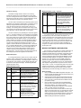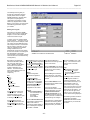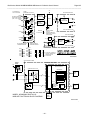
1
BusWorks 900MB Series Modbus/RS485 Network I/O Modules Model 901MB/902MB/903MB Digital Input/Output With Sinking Outputs And Active-Low Inputs USER’S MANUAL ACROMAG INCORPORATED 30765 South Wixom Road P.O. BOX 437 Wixom, MI 48393-7037 U.S.A. Tel: (248) 624-1541 Fax: (248) 624-9234 Copyright 2000, Acromag, Inc., Printed in the USA. Data and specifications are subject to change without notice. 8500-631-H06J010 BusWorks Model 903MB/902MB/901MB Network I/O Module User’s Manual Digital I/O ___________________________________________________________________________________________ Safety Summary - Symbols on equipment: IMPORTANT SAFETY CONSIDERATIONS ! It is very important for the user to consider the possible adverse effects of power, wiring, component, sensor, or software failures in designing any type of control or monitoring system. This is especially important where economic property loss or human life is involved. It is important that the user employ satisfactory overall system design. It is agreed between the Buyer and Acromag, that this is the Buyer's responsibility. Means “Caution, refer to this manual for additional information”. The information contained in this manual is subject to change without notice. Acromag, Inc., makes no warranty of any kind with regard to this material, including, but not limited to, the implied warranties of merchantability and fitness for a particular purpose. Further, Acromag, Inc., assumes no responsibility for any errors that may appear in this manual and makes no commitment to update, or keep current, the information contained in this manual. No part of this manual may be copied or reproduced in any form, without the prior written consent of Acromag, Inc. Table of Contents 1.0 INTRODUCTION ………………………………..…….. DESCRIPTION ………………………………………… Key 903MB Features……………………………….. ACCESSORY ITEMS …………………………………. 2.0 PREPARATION FOR USE ….……………………….. UNPACKING AND INSPECTION …………………… MODULE INSTALLATION.……………..…………….. Default Mode Switch………………………………… Pullup Installation & Removal………………………. Mounting ……………………………………………… Electrical Connections ……………………………… SOFTWARE INSTALLATION ……………….……….. 3.0 MODULE CONFIGURATION ……………………….. REGISTER MAP……………………………………….. AN INTRODUCTION TO MODBUS………………..... MODULE SOFTWARE CONFIGURATION…………. Starting The Program…..…………………………… Creating A Configuration File……………………….. Testing Your Configuration….……………………… 4.0 THEORY OF OPERATION ………………………….. 5.0 SERVICE AND REPAIR …………………………..… SERVICE AND REPAIR ASSISTANCE ……………. PRELIMINARY SERVICE PROCEDURE ..…………. TROUBLESHOOTING………………………………… 6.0 SPECIFICATIONS ……………………………………. MODEL NUMBER DEFINITION……………………… I/O SPECIFICATIONS……………….…………..……. ENCLOSURE/PHYSICAL SPECIFICATIONS..…….. APPROVALS ………………………………………….. ENVIRONMENTAL SPECIFICATIONS….………….. COMMUNICATION INTERFACE SPECIFICATIONS CONFIGURATION AND CONTROLS..……………... SOFTWARE CONFIGURATION……..…………….… List of Drawings Simplified Schematic (4501-809)…..…….……………..… Functional Block Diagram (4501-810)………………….… Pullup Resistor SIP Locations (4501-811)……………….. Network Connections (4501-805)…………..…….………. Electrical Connections Page 1 of 4 (4501-813)……..…... Electrical Connections Page 2 of 4 (4501-813)……..…... Electrical Connections Page 3 of 4 (4501-813)……..…... Electrical Connections Page 4 of 4 (4501-813)……..…... Interposing Relay Conn. & Contact Pro. (4501-814)……. Enclosure Dimensions (4501-815) …………………..…… 1.0 INTRODUCTION These instructions cover the hardware functionality of the transmitter models listed in Table 1. Supplementary sheets are attached for units with special options or features. Page Table 1: Models Covered in This Manual -Factory Series/ -Options/Output/ Input Type Enclosure/ Approvals1 Config2 I/O Type 901MB -0900 -C 12 Inputs 902MB -0900 -C 12 Outputs 903MB -0900 -C 12 In/Out 2 2 3 3 4 4 4 4 5 5 5 6 6 6 8 15 16 17 18 19 19 19 19 19 20 20 20 21 21 21 22 22 22 Notes (Table 1): 1. Agency approvals include CE, UL Listed, and cUL Listed. 2. Include the “-C” suffix to specify factory configuration option. Otherwise, no suffix is required for standard configuration. 3. The 903MB includes both inputs and outputs, while the 902MB is output only, and the 901MB is input only. The same circuit board is used to build all three models listed. The fully populated 903MB model includes tandem input and output circuits. Input circuitry is removed for 902MB models which are output only, and output circuitry is removed for 901MB models which are input only. DESCRIPTION The Acromag 900MB family is a group of process I/O modules and accessories for Modbus/RS485 network I/O applications. The 901MB/902MB/903MB models support up to twelve buffered inputs and/or open-drain outputs according to the model number. Inputs are active-low and outputs are currentsinking low-side switches. These models are the complement of Acromag 904MB/905MB/906MB modules which have opensource high-side output switches and active-high inputs. The 900MB modules contain an advanced technology microcontroller with integrated downloadable flash memory and EEPROM for non-volatile program, configuration, and parameter data storage. Units are fully reconfigurable via our user-friendly Windows 95/98 or NT Configuration Program and the RS485 interface. Once configured, these modules may operate as active RS485 network slaves connected to other modules and a host computer performing network I/O functions. Page 24 24 25 25 26 26 27 27 28 28 The Model 901MB supports up to 12 digital inputs. The Model 902MB drives up to 12 digital outputs. The Model 903MB supports up to 12 tandem digital input and output channels. Each 900MB module provides an isolated RS485 network I/O path utilizing the Modbus protocol. Socketed I/O pullup resistors are installed and pull the I/O channels up to the EXC+ terminal. These resistors may be easily removed or exchanged according to your application requirements. Windows 95/98 & NT are registered trademarks of Microsoft Corporation. Modbus is a registered trademark of Modicon, Inc. -2- BusWorks Model 903MB/902MB/901MB Network I/O Module User’s Manual Digital I/O ___________________________________________________________________________________________ Key 903MB Module Features…continued: I/O channels include yellow LED’s on the front of the module that provide visual indication of channel state. Additionally, a green “Run” and yellow “Status” LED provides local feedback of operating mode, system diagnostics, watchdog timeout indication, and module status. • • All 900MB modules are designed to withstand harsh industrial environments. They feature RFI, EMI, ESD, EFT, and surge protection, plus low temperature drift, wide ambient temperature operation, and isolation between input, outputs, power, and the network. They also have low radiated emissions per CE requirements. As a wide-range DC-powered device, the unit may be powered from DC power networks incorporating battery backup. Since the input is diode bridge coupled, the unit may be connected to redundant power supplies, or several units may safely share a single DC supply. The unit may also be powered from common 24VAC power. • Units are DIN-rail mounted and removable terminal blocks facilitate ease of installation and replacement, without having to remove wiring. Module power and network wiring are inserted at one side of the unit, while I/O wiring is inserted at the other side. Module connectors are an industry standard screw clamp type that accept a wide range of wire sizes. • Flexible transmitter functionality, network reprogrammability, mixed signal I/O, watchdog support, and a network interface, are all combined in a single package to make this instrument extremely powerful and useful over a broad range of applications. Further, the safe, compact, rugged, reconfigurable, and reliable design of this transmitter makes it an ideal choice for control room or field applications. Custom module configurations are also possible (please consult the factory). • • • • Key 903MB Module Features: • • • • • • • • • Agency Approvals - CE, UL, & cUL Listed. Easy Windows Configuration - Fully reconfigurable via our user-friendly Windows 95/98 or NT 900MB Configuration Program. RS485/Modbus Network Interface - This proven high speed interface is highly immune to noise, can operate over long distances, and allows a large number of modules to be networked together. The unit communicates using the industry-standard Modbus command/response protocol. Nonvolatile Reprogrammable Memory - This module has an advanced technology microcontroller with integrated, non-volatile, downloadable flash memory and EEPROM. This allows the functionality of this device to be reliably reprogrammed thousands of times. Fully Isolated – I/O circuitry, network, & power are isolated from each other for safety and increased noise immunity. Flexible Discrete Inputs and Outputs - High voltage, high current, open-drain outputs provide direct (low-side) control of external devices. High voltage buffered inputs allow outputs to be read back, or input levels to be monitored. Outputs Have Built-in Protection – Outputs include overtemperature and over-current shut-down protection, plus active clamping circuitry for switching inductive loads. Tandem Input/Output Circuitry (903MB Units) - Input buffers are connected in tandem with open-drain outputs for convenient loopback monitoring of the output state. High-Speed Data Rates – Supports half-duplex RS485 baud rates up to 115K baud. • Convenient Pullup Resistors Mounted In Sockets – SIP resistors are installed in sockets on the board and provide input/output pullup functionality. These SIP resistors can be easily removed or exchanged according to your application. Self-Diagnostics - Built-in routines operate upon power-up for reliable service, plus easy maintenance and troubleshooting. A watchdog timer is also built into the microcontroller that causes it to initiate a self reset if it ever fails to return from an operation in a timely manner or “locks up”. I/O Watchdog Timer – This function is included and may be configured for timeout periods up to 65534 seconds (18.2 hours). A timeout will occur if no port channel I/O has taken place for the specified time period. Optionally, the digital outputs can be automatically set to a user-defined state following a watchdog timeout. A port timeout is cleared via a read or write to a port I/O channel. Watchdog control of an output state has higher priority than direct control. Wide-Range DC or 24VAC Power - This device receives power over a wide supply range and the power terminals are diode-bridge coupled. This makes this transmitter useful for systems with redundant supplies, and/or battery back-up. Additionally, the power terminals are not polarized. Wide Ambient Operation - The unit is designed for reliable operation over a wide ambient temperature range. Hardened For Harsh Environments - The unit will operate reliably in harsh industrial environments and includes protection from RFI, EMI, ESD, EFT, and surges, plus low radiated emissions per CE requirements. Convenient Mounting, Removal, & Replacement - The DIN-rail mount and plug-in type terminal blocks make module removal and replacement easy. LED Indicators - A green LED indicates power. A flashing yellow status LED indicates the unit is in the default communication mode and/or a watchdog timer timeout has occurred. Yellow LED’s also indicate the I/O state (activelow) of the associated open-drain output and/or digital input. Default Communication Mode - A push-button switch is provided to set the module to a default set of communication parameters for baud rate, module address, parity, and number of stop bits. This provides a convenient way of establishing communication with the module when its internal settings are unknown. ACCESSORY ITEMS The following accessories are available from Acromag. Acromag also offers other standard and custom transmitters and alarms to serve a wide range of applications (consult the factory). 900MB Configuration & Control Software (Model 5034-186) Series 900MB modules are configured with this user-friendly Windows 95/98 or NT Configuration Program. Optionally, any software that supports the Modbus/RTU protocol may be used to configure and control Series 900MB modules, but the use of this software makes getting started easier. All module functions are programmable and downloadable to the modules via this software. The software also includes on-line help. Non-volatile memory provides program and configuration storage within the module. Note that this software may be optionally downloaded from our website (www.acromag.com) to registered owners of Series 900MB modules. -3- BusWorks Model 903MB/902MB/901MB Network I/O Module User’s Manual Digital I/O ___________________________________________________________________________________________ RS-232 to RS-485 Serial Adapter (Model 5034-214) MODULE INSTALLATION This device is a non-isolated, port-powered, signal converter for communication between the RS-232 serial port of a personal computer and the RS-485 network interface of Series 900MB I/O Modules. It is used in conjunction with the Acromag Configuration Software for simple reconfiguration, testing, and troubleshooting of Series 900MB I/O modules. As a portpowered device, it is not intended for driving fully loaded RS-485 networks over long distances, and does not have sufficient power to drive terminated networks. The adapter has DB-9F connectors at both ends and plugs directly into the common DB-9M serial port connector of most personal computers. The module is connected to the RS-485 side of this adapter via a separate interconnecting cable (see Cable 5034-202 described below). This transmitter module is packaged in a general purpose plastic enclosure. Use an auxiliary enclosure to protect the unit in unfavorable environments or vulnerable locations, or to maintain conformance to applicable safety standards. Stay within the specified operating temperature range. As shipped from the factory, the unit is calibrated for all valid input ranges and has the default configuration shown in Table 2 below: WARNING: Applicable IEC Safety Standards may require that this device be mounted within an approved metal enclosure or sub-system, particularly for applications with exposure to voltages greater than or equal to 75VDC or 50VAC. Table 2: 903MB Default Factory Configuration PARAMETER CONFIGURATION Module Address 247 Baud Rate 9600bps Parity None Stop Bits 1 or 2 (When Parity = None) Response Delay 0 (No Additional Delay) Watchdog Time (Each Port) 0 (Disabled) Timeout State (Each Port) 65535 (FFFFH) = No Change Pullup Resistor To EXC+ 5.6K Installed (In Sockets) Interface Cable (Model 5034-202) This 3-wire cable is used to connect the RS-485 side of Signal Converter 5034-214 to the RS-485 network terminals of Series 900MB modules. This cable is 8 feet long and has a DE-9M connector on one end, and three stripped and tinned wires on the other end. The wires are labeled A, B, and C for connection to the module D, Dbar, and COM terminals, respectively. Note: Do not confuse the Default Factory Configuration noted above with the Default Communication Mode, which refers to the fixed baud rate, module address, parity, and stop bit settings achieved by pushing the Default Mode button until the status LED flashes ON/OFF. The Default Communication Mode will temporarily over-ride any factory configuration of baud rate, module address, parity, and stop bits with settings of 9600bps, 247, None, and 1 or 2, respectively. It is provided as a convenient means of achieving communication with a module when these parameters are unknown. Series 900MB Software Interface Package (Model 900C-SIP) The 900C-SIP Software Interface Package combines the 900MB Configuration Software (5034-186), RS-232 to RS-485 Serial Converter (5034-214), Interface Cable (5034-202), and Instructions (8500-649), into a complete kit for interfacing with Series 900MB I/O Modules. 2.0 PREPARATION FOR USE Your application will typically differ from the default factory configuration and will require that the transmitter be reconfigured to suit your needs. This can be easily accomplished with Acromag’s user-friendly Windows 95/98 or NT 900MB Configuration Program. Configuration is normally done prior to field installation. Refer to MODULE SOFTWARE CONFIGURATION of Section 3.0 for detailed instructions. UNPACKING AND INSPECTION Upon receipt of this product, inspect the shipping carton for evidence of mishandling during transit. If the shipping carton is badly damaged or water stained, request that the carrier's agent be present when the carton is opened. If the carrier's agent is absent when the carton is opened and the contents of the carton are damaged, keep the carton and packing material for the agent's inspection. For repairs to a product damaged in shipment, refer to the Acromag Service Policy to obtain return instructions. It is suggested that salvageable shipping cartons and packing material be saved for future use in the event the product must be shipped. Default Mode Switch A push-button default mode switch (DFT) and status LED are provided at the front of the module as a convenient way of communicating with the module when its baud rate and address settings are unknown. Push & hold this button until the Status LED flashes ON/OFF to indicate the module is in the Default Communication Mode with a fixed module address of 247, baud rate of 9600bps, no parity, and 1 or 2 stop bits. It is most convenient to configure a module in this mode, then leave the default mode by pressing this button again until the Status LED stops flashing (constant ON or OFF), or by resetting the module. Note that a rapidly flashing Status LED indicates a watchdog timer timeout has occurred and this may temporarily mask default mode indication. The Default Mode is disabled following a software or power-on reset. New communication parameters (for baud rate, address, and parity) will take effect following a reset of the module and the module will leave the Default Mode. This module is physically protected with packing material and electrically protected with an anti-static bag during shipment. However, it is recommended that the module be visually inspected for evidence of mishandling prior to applying power. This circuit utilizes static sensitive components and should only be handled at a static-safe workstation. -4- BusWorks Model 903MB/902MB/901MB Network I/O Module User’s Manual Digital I/O ___________________________________________________________________________________________ Pullup Installation & Removal (See Drawing 4501-811) It is recommended that I/O, network, and power wiring be separated for safety, as well as for low noise pickup. Note that I/O, network, and power terminal blocks are an industry-standard plug-in type that can be easily removed to facilitate module removal or replacement, without removing individual wires. Be sure to remove power before unplugging the terminals to uninstall the module, or before attempting service. All connections must be made with power removed. Sockets are installed on the board to accept SIP resistor networks for optional I/O pullup installation. One 8-pin SIP socket is provided for every four I/O channels (port). These 8-pin sockets accept SIP’s of four isolated resistors with the evennumbered socket pins in common with the EXC+ terminal. Three 5.6KΩ resistor SIP’s are installed from the factory, but may be changed or removed as required by your application. The cover must be removed to access these sockets (see Drawing 4501-811). For the 5.6K resistor SIP provided, power must be limited to less than 0.4W per resistor element. Limit excitation voltages to 35V or less, and drain currents to less than 0.5A. Your choice of SIP resistor may further limit current and voltage according to its power rating (ratings of 0.2W, 0.3W, or 0.4W per resistor element are typical). Refer to the I/O Specifications section for recommended resistor types and suppliers. CAUTION: Risk of Electric Shock - More than one disconnect switch may be required to de-energize the equipment before servicing. 1. Power: Refer to Electrical Connections Drawing 4501-813. Variations in power supply voltage within rated limits has negligible effect on module accuracy. For supply connections, use No. 14 AWG wires rated for at least 75°C. The power terminals are diode bridge-coupled and not polarized. Unit is powered from 10-36VDC, or 24VAC only. 2. Digital I/O: Connect I/O per Electrical Connections Drawing 4501-813. Observe proper polarity when making I/O connections (see label for input type). All outputs are the open-drains of n-channel mosfets whose source terminals share return (RTN). I/O pullup resistor SIP’s are installed in sockets on the board and connected to the port EXC+ terminal. All terminals include transient voltage suppression and integrated snubbers, but may require additional protection when switching inductive loads (see below). Refer to the SPECIFICATIONS section for output specifications and see the module side label for terminal designations. Note that outputs are for current-sinking (low-side switching) applications only. Inputs are active-low. The I/O circuitry is electrically isolated from the power and network circuits. If necessary, an interposing relay can be used to switch higher currents as illustrated in the Interposing Relay Connection Drawing 4501-814. IMPORTANT: You must provide I/O excitation to operate the outputs and prevent inputs from floating. You may utilize the internal 5.6K pullup resistors installed in sockets on the board by connecting a 5-35V excitation supply to the port EXC & RTN terminals to complete the circuit. Optionally, the internal pullups may be removed and the I/O terminals can be wired to an external pullup or load/excitation circuit in similar fashion. If your application delivers power to the I/O terminal rather than the port excitation terminal, then the port pullups should be removed to avoid coupling currents to adjacent port channels via the pullup resistors. Outputs are the open drains of n-channel mosfets in series with output pullup resistors tied in common to the port EXC terminal. Input circuits utilize these same pullups to the port EXC terminal. Failure to complete this circuit by providing an excitation supply and/or pullups will leave the inputs and outputs floating and/or inoperable (Refer to Simplified Schematic 4501-809). Mounting Note: Outputs go to their OFF state following a software or power-on reset of the module. Outputs may be optionally sent to user-defined states following a watchdog timeout. Refer to Enclosure Dimensions Drawing 4501-815 for mounting and clearance dimensions. IMPORTANT - Protection With Inductive Loads: The output DMOS type mosfets have integrated shunt diode clamps connected from drain to source to help protect the output switch from damaging reverse emf voltages that are generated when switching inductive loads. You are encouraged to add external protection local to the inductive load for added protection and to prevent this emf from being distributed across the connection media. For DC inductive loads, place a diode across the load (1N4006 or equivalent) with cathode to (+) and anode to (-). DIN Rail Mounting: This module can be mounted on "T" type DIN rails. Use suitable fastening hardware to secure the DIN rail to the mounting surface. Units may be mounted side-by-side on 1-inch centers for limited space applications. "T" Rail (35mm), Type EN50022: To attach a module to this style of DIN rail, angle the top of the unit towards the rail and locate the top groove of the adapter over the upper lip of the rail. Firmly push the unit towards the rail until it snaps solidly into place. To remove a module, first separate the input terminal block(s) from the bottom side of the module to create a clearance to the DIN mounting area. Next, insert a screwdriver into the lower arm of the DIN rail connector and use it as a lever to force the connector down until the unit disengages from the rail. 3. Network Connections: Wire network as shown in Network Connections Drawing 4501-805. Network common (COM) should connect to earth ground at one point. 4. Grounding: See Electrical Connections Drawing 4501-813. The module housing is plastic and does not require an earth ground connection. Electrical Connections Digital I/O, network, and power terminals can accommodate wire from 12-24 AWG, stranded or solid copper. Strip back wire insulation 1/4-inch on each lead before installing into the terminal block. Since common mode voltages can exist on signal wiring, adequate wire insulation should be used and proper wiring practices followed. WARNING: For compliance to applicable safety and performance standards, the use of shielded cable is recommended as shown in Drawing 4501-813. Further, the application of earth ground must be in place as shown in Drawing 4501-813. Failure to adhere to sound wiring and grounding practices may compromise safety & performance. -5- BusWorks Model 903MB/902MB/901MB Network I/O Module User’s Manual Digital I/O ___________________________________________________________________________________________ SOFTWARE INSTALLATION - USING SETUP.EXE Reference 0xxxx The 900MB Configuration Software (Model 900C-SIP) is used to configure Series 900MB modules and is installed as follows: 1xxxx 1. Start Windows 95/98/NT and insert the 900MB Configuration Software CDROM into your drive D: (or E:). IMPORTANT: Before continuing with installation, be sure to exit any other Windows programs that may be running. 2. Click on the [START] button in the lower left hand corner of the Windows screen. Then click on the “Run…” icon. 3. In the Run dialogue box, type d:\setup (or e:\setup) in the Open field and click on [OK]. The setup program will execute the Installshield Wizard. You may need to click on the “Setup.exe” icon of the install shield to proceed. On some machines, the setup.exe program is not started automatically. 4. From the introductory Acromag 900MB Setup Screen, click on [Next>] to proceed. 5. At this point, the 900MB Setup program will prompt you for your “Name” and “Company”. Fill in this information, then click on [Next>]. 6. Now you will be prompted for a destination directory. You may click on [Browse] to change the default directory, or [Next>] to accept “C:\ProgramFiles\Acromag\900MB” as the default. You may also click on [Back] to return to the prior screen and make any changes. 7. At this point you will be prompted for a program folder name. You may type a new name, use the scroll bar to select an existing program folder, or click on [Next>] to accept the “Acromag 900MB” default folder name. 8. Now you will be presented with your selections and you should verify if they are correct. Press [Next>] to continue and begin copying files, or press [Back] to return to prior screens and make any changes. 9. After the Configuration Program files have been copied to your hard drive, you will be prompted to click on [Finish] to complete the setup. 10. Now click on the [Acromag 900MB] program folder icon at the bottom of your windows screen, then click on the Acromag 900MB program icon to start the Configuration Program (Programs-Acromag 900MB-Acromag 900MB Configuration icon). 3xxxx 4xxxx Description Read/Write Discrete Outputs or Coils. A 0x reference is used to drive output data to a digital output channel. Read Discrete Inputs. The ON/OFF status of a 1x reference is controlled by the corresponding digital input channel. Read Input Registers. A 3x reference register contains a 16-bit number received from an external source—e.g. an analog signal. Read/Write Output or Holding Registers. A 4x register is used to store 16-bits of numerical data (binary or decimal), or to send the data from the CPU to an output channel. Notes: 1. The “x” following the leading character represents a fourdigit address location in user data memory. The leading character is generally implied by the function code and omitted from the address specifier for a given function. The leading character identifies the I/O data type. 2. The ON/OFF state of discrete inputs and outputs is represented by a 1 or 0 value assigned to an individual bit in a 16-bit data word. This is sixteen 0x or 1x references per data word. With respect to mapping, the LSB of the word maps to the lowest numbered channel of a group and channel numbers increase sequentially as you move towards the MSB. Unused bit positions are set to zero. The table below outlines the register map for Model 901MB/902MB/903MB network I/O modules. Modbus functions operate on these registers (except for the Reset Slave and Report Slave ID functions). Model 903MB-0900 Register Map Ref Addr. Description Data Type/Format Coil Registers (0x References, Read/Write) Discrete Output Value. Twelve 0-11 00001 Addresses a specific bit of (0000- Discrete Thru a 16-bit word that controls/ Outputs 0-11 000B) 00012 monitors the ON/OFF (903MB & 902MB Only) status for the output (the gate signal of the nchannel mosfet). A set bit (1) means the corresponding output is Note: This signal corresponds to turned ON (sinking the gate signal of the n-channel current). A clear bit (0) output mosfet. Thus, a read of means the corresponding this register may not reflect the output is turned OFF actual output level at the drain of the mosfet if the open-drain is not (open). The bit position also corresponds to the pulled up or is left floating. output channel number (i.e. Excitation must be provided in output 0 uses bit 0 of the order to operate the outputs. On 16-bit word at address 0, 903MB units, you can read the output 1 uses bit 1 of the Contact Registers to obtain the 16-bit word at address 1, actual output state(s) via closed etc.) Unused bits are set loop feedback. to 0. After reset, these registers read 0 Bits 15-12: Not Used. (outputs OFF) and these Additionally, unused bits registers are not maintained in in range 11-0 are set to 0. EEPROM. 3.0 MODULE CONFIGURATION This module needs to be configured for your application. Configuration is easily accomplished using Acromag’s Windows 95/98 or NT Modbus Configuration Software and an RS232-toRS485 signal converter. It is not required to use the Acromag software to communicate with the Series 900MB, as any software capable of sending Modbus protocol commands over an RS485 network can be used. However, the Acromag software provides an easy to use Windows format for communicating with the module that does not require advanced familiarity with the Modbus protocol. REGISTER MAP Modbus registers are organized into the following reference types identified by the leading number of the reference address: -6- BusWorks Model 903MB/902MB/901MB Network I/O Module User’s Manual Digital I/O ___________________________________________________________________________________________ Model 903MB-0900 Register Map…continued Ref Addr. Description Data Type/Format Contact Registers (1x References, Read-Only) Discrete Input Value. Twelve 0-11 10001 Addresses a specific bit of (0000- Discrete Thru a 16-bit word that monitors Inputs 0-11 000B) 10012 the ON/OFF status for the (903MB & 901MB Only) input (or tandem output). A set bit (1) means the corresponding input is ON Note: This signal reflects the (active-low). A clear bit (0) actual state of the corresponding means the corresponding input signal (901MB & 903MB), input is OFF (high). The bit or the drain of the tandem output position corresponds to the (903MB). This signal is activeinput channel number (i.e. low. input 0 uses bit 0 of the 16bit word at address 0, input Failure to install I/O pullups or 1 uses bit 1 of the 16-bit provide port excitation will leave word at address 1, etc.) inputs floating. Unused bits of a word are set to 0. Bits 15-12: Not Used. Additionally, unused bits in range 11-0 are set to 0. Input Registers (3x References, Read-Only) 30001 0000 Module Bit 15: Flash Checksum 1 = Error Flag Status 0 = No Flash Error Bit 14: Zero (Not Used) Bit 13: Default Mode Flag 1 = Default Mode Indicator 0 = Not Default Mode Bits 12-3: Zero Bit 2: Port 2 (CH 8-11) 1 = Port 2 Watchdog Fault Bit 1: Port 1 (CH 4-7) 1 = Port 1 Watchdog Fault Bit 0: Port 0 (CH 0-3) 1 = Port 0 Watchdog Fault Holding Registers (4x References, Read/Write) Note: Changes to Holding Registers take effect following the next software or power-on reset of the module. 1-247 40001 0 Slave (0000) Address Default=247 0 = 2400bps 40002 1 Baud Rate 1 = 4800bps (0001) Default=2, 2 = 9600bps (Default) 9600bps 3 = 14400bps 4 = 19200bps 5 = 28800bps 6 = 38400bps 7 = 57600bps 8 = 76800bps 9 = 115200bps 0 = None (1 or 2 stop bits) 40003 2 Parity 1 = Odd Parity Checking (0002) Default= 2 = Even Parity Checking 0, None Model 903MB-0900 Register Map…continued Ref Addr. Description Data Type/Format 3 Port 0 40004 Can be set from 1 to 65534 (0003) (CH0-3) seconds. Set to 65535 Watchdog (FFFFH) or 0 (0000H) to Time disable the watchdog timer. Default=0, Disabled Note: A port timeout can only be cleared via a read or write to any channel of the same port, or upon a software or power-on reset of the module. 4 Port 1 40005 Can be set from 1 to 65534 (0004) (CH 4-7) seconds. Set to 65535 Watchdog (FFFFH) or 0 (0000H) to Time disable the watchdog timer. Default=0, Disabled 5 Port 2 40006 Can be set from 1 to 65534 (0005) (CH 8-11) seconds. Set to 65535 Watchdog (FFFFH) or 0 (0000H) to Time disable the watchdog timer. Default=0, Disabled 6 Port 0 40007 The four lower order bits of (0006) (CH 0-3) this 16-bit register value Timeout define the state the output State channels of the port will be (902MB and programmed to following a 903MB Only) watchdog timeout. Bit 0 corresponds to channel 0, Default= bit 1 to channel 1, bit 2 to 65535, channel 2, and bit 3 to Disabled. channel 3. Note: Clearing a timeout via an Write 65535 (FFFFH) to I/O read or write does not return this register to leave the the output(s) to their initial state. outputs unchanged They remain in their timeout following a timeout (this is states until otherwise written. also the default value). 7 Port 1 40008 The four lower order bits of (0007) (CH 4-7) this 16-bit register value Timeout define the state the output State channels of the port will be (902MB and programmed to following a 903MB Only) watchdog timeout. Bit 0 corresponds to channel 4, Default= bit 1 to channel 5, bit 2 to 65535, channel 6, and bit 3 to Disabled. channel 7. Write 65535 (FFFFH) to this register to leave the outputs unchanged following a timeout (this is also the default value). -7- BusWorks Model 903MB/902MB/901MB Network I/O Module User’s Manual Digital I/O ___________________________________________________________________________________________ Notes (Register Map)…continued: 2. For your convenience, this module mirrors the contents and operation of 3xxxx registers into 43xxx holding register space for systems and controllers that cannot directly access 3xxxx registers. That is, the 3xxxx registers of this model can be written to, or read from, using either the standard methods described in the Modbus specification, or through mapping (mirroring) to the Holding Register space. The format of the registers are identical and you only need to offset your address by 43000. For example: if you want to read Input Register 1 through the Holding Registers, you would use the “Read Holding Registers” function with an address of 43001. 3. For modules with a firmware revision later than G (as in 9300-029G of 901MB, 9300-030G of 902MB, and 9300031G of 903MB), the mirroring function as described in Note 2 is augmented as follows (0xxxx also maps to 42xxx space, and 1xxxx also maps to 41xxx space): Model 903MB-0900 Register Map…continued Ref Addr. Description Data Type/Format Holding Registers (4x References, Read/Write) 8 Port 2 40009 The four lower order bits of (0008) (CH 8-11) this 16-bit register value Timeout define the state the output State channels of the port will be (902MB and programmed to following a 903MB Only) watchdog timeout. Bit 0 corresponds to channel 8, Default= bit 1 to channel 9, bit 2 to 65535, channel 10, and bit 3 to Disabled. channel 11. Write 65535 (FFFFH) to this register to leave the outputs unchanged following a timeout (this is also the default value). 40010 9 Response Can be set from 0 to 65500 (0009) Delay Time ticks (1 tick = 1.085us). (Turnaround This is the additional delay Delay) the module will wait before responding to a message Default=0, from the host. Increase No Delay this value if you have trouble communicating with the module or you encounter a high degree of error messages. Writing 41429 (A1D5H) to 40011 10 Alternate this register will cause a (000A) Method of module reset. This is Module provided as an alternate Reset method of Reset for software that does not support the Reset Slave (08) command. For 1xxxx Input Status Registers (where supported), the return data is reformatted to match the Holding Register format. For example, if you request Input Status for 12 digital inputs, instead of getting 2 bytes returned with the first 12 bits representing 12 digital inputs, you will get 12 separate words (2 bytes) instead, with each set to 0000H (OFF) or FFFFH (ON). For 0xxxx Coil Registers (where supported), reads are handled in the same way as noted for 1xxxx Input Status Registers. That is, you may write to the coil registers using the “Preset Single Register” function with an address offset of 42000. Setting the data to 0000H will turn the coil OFF, while setting the data to FF00H will turn the coil ON. AN INTRODUCTION TO MODBUS The Modbus protocol provides an industry standard method that Series 900MB modules use for parsing messages. Modbus devices communicate using a master-slave technique in which only one device (the master) can initiate transactions (called queries). The other devices (slaves) respond by supplying the requested data to the master, or by taking the action requested in the query. The Series 900MB modules are slaves, while a typical master device is a host computer running appropriate application software. Masters can address individual slaves, or can initiate a broadcast message to all slaves. Slaves return a response to all queries that are addressed to them individually, but no response is returned to broadcast queries from a master device. After a reset, this register reads 0 (no reset). 41001 . . . This block mirrors 1xxxx registers. 42001 . . . This block mirrors 0xxxx registers. 43001 . . . This block mirrors 3xxxx registers. This register is not maintained in EEPROM. Refer to Note 3. 1xxxx Discrete Input Registers are mapped to the 41xxx Holding Register space using an address offset of 41000. Refer to Note 3. 0xxxx Coil Registers are mapped to the 42xxx Holding Register space using an address offset of 42000. Refer to Note 2. 3xxxx Input registers are mapped to the 43xxx Holding Register space using an address offset of 43000. Remote Terminal Unit (RTU) Mode The Series 900MB modules use the widely accepted Modbus network protocol in the RTU (Remote Terminal Unit) serial transmission mode. In RTU mode, each 8-bit message byte contains two 4-bit hexadecimal characters, and the message is transmitted in a continuous stream. The format for each byte in RTU mode is outlined below: RTU Mode Byte Format Coding System 8-bit binary, hexadecimal 0-9, A-F, two hexadecimal characters contained in each 8-bit field of the message. Bits Per Byte 1 start bit + 8 data bits, lsb sent first + 1bit for even/odd parity or no bit for no parity + 1 stop bit if parity is used, or 1 or 2 stop bits with no parity. Error Check Field Cyclical Redundancy Check (CRC) Notes (Register Map): 1. Configuration variables stored in holding registers (4xxxx reference addresses) are maintained in EEPROM except as noted. Changes to these register parameters do not take effect until the next software or power-on reset of the module. -8- BusWorks Model 903MB/902MB/901MB Network I/O Module User’s Manual Digital I/O ___________________________________________________________________________________________ A master’s query is comprised of a slave address (or broadcast), a function code defining the requested action, any data required, and an error checking field. A slave’s response is comprised of fields confirming the action taken, any data to be returned, and an error checking field. The query and response both include a device address + function code + data byte(s) + error checking field. If an error occurred in the receipt of the query, or if the slave is unable to perform the requested action, the slave will return an exception message as its response (see Modbus Exceptions). The error check field allows the master to confirm that the message contents are valid. Modbus Addresses Modbus Message Framing With respect to data addresses, all data addresses in Modbus messages are referenced to 0, with the first occurrence of a data item addressed as item number zero. Further, a function code field already specifies which register group it is to operate on (i.e. 0x, 1x, 3x, or 4x reference addresses). For example, holding register 40001 is addressed as register 0000 in the data address field of the message. The function code that operates on this register specifies a “holding register” operation and the “4xxxx” reference is implied. Holding register 40108 is addressed as register 006BH (107 decimal). The master device addresses a specific slave device by placing the 8-bit slave address in the address field of the message. Valid addresses are from 1-247. When the slave responds, it places its own address in this field of its response to let the master know which slave is responding. Address 0 is reserved for the broadcast address, which all slave devices on a network recognize. A slave does not issue a response to broadcast messages. Further, not all function messages support the broadcast address. A Modbus message is placed in a frame by the transmitting device. A frame is used to mark the beginning and ending point of a message allowing the receiving device to determine which device is being addressed and to know when the message is completed. It also allows partial messages to be detected and errors flagged as a result. RTU mode messages start with a silent interval of at least 3.5 character times implemented as a multiple of character times at the baud rate being used on the network (indicated as t1t2t3t4 below). The first field transmitted is the device address. The allowable characters transmitted for all fields are hexadecimal values 0-9, A-F. A networked device continuously monitors the network, including the silent intervals, and when the first field is received (the address), the device decodes it to determine if it is the addressed device. Following the last character transmitted, a similar silent interval of 3.5 character times marks the end of the message and a new message can begin after this interval. A typical message frame is shown below. RTU Message Frame Start Addr. Function t1t2t3t4 8 bits 8 bits Data nx8 bits CRC 16 bits Modbus Functions The function code field of a message frame contains the 8 bits that tell the slave what kind of action to take. Valid codes are in the range 1-255. Not all codes apply to a module and some codes are reserved for future use. The following table highlights the subset of standard Modbus functions supported by the Model 901MB/902MB/903MB modules (the reference register addresses that the function operates on are also indicated): CODE 01 (01H) 02 (02H) 03 (03H) 04 (04H) 05 (05H) 06 (06H) 08 (08H) 15 (0FH) 16 (10H) 17 (11H) End t1t2t3t4 The entire message must be transmitted as a continuous stream. If a silent interval of more than 1.5 character times occurs before completion of the frame, the receiving device flushes the incomplete message and assumes the next byte will be the address field of a new message. In similar fashion, if a new message begins earlier than 3.5 character times following a previous message, the receiving device assumes it is a continuation of the previous message. This will generate an error, as the value in the final CRC field will not be valid for the combined messages. When a slave device responds to the master, it uses the function code field to indicate either a normal (error-free) response, or that some kind of error has occurred (an exception response). A normal response simply echoes the original function code of the query, while an exception response returns a code that is equivalent to the original function code with its most significant bit (msb) set to a logic 1. For example, the Read Holding Registers command has the function code 0000 0011 (03H). If the slave device takes the requested action without error, it returns the same code in its response. But if an exception occurs, it returns 1000 0011 (83H) in the function code field and appends a unique code in the data field of the response message that tells the master device what kind of error occurred, or the reason for the exception (See Modbus Exceptions). When messages are transmitted on Modbus serial networks, each character or byte is sent in order of Least Significant Bit (LSB) to Most Significant Bit (MSB) as noted below (left to right): 6 7 Stop Stop 6 7 Parity Stop REFERENCE 0xxxx 1xxxx 4xxxx 3xxxx 0xxxx 4xxxx Hidden 0xxxx 4xxxx Hidden These functions are used to access the registers outlined in the register map presented in the prior section for sending and receiving data. Note that the Report Slave ID and Reset Slave commands do not operate on register map registers. How Characters Are Transmitted Serially RTU Character Framing (No Parity) Start 0 1 2 3 4 5 RTU Character Framing (With Parity) Start 0 1 2 3 4 5 FUNCTION Read Coil (Output) Status Read Input Status Read Holding Registers Read Input Registers Force Single Coil (Output) Preset Single Register Reset Slave Force Multiple Coils (Outputs) Preset Multiple Registers Report Slave ID Note that an additional stop bit is normally transmitted to fill out the character frame for no parity. Acromag units will accept one or two stop bits with no parity. -9- BusWorks Model 903MB/902MB/901MB Network I/O Module User’s Manual Digital I/O ___________________________________________________________________________________________ The master’s application program must handle the exception response. It may choose to post subsequent retries of the original message, it may try sending diagnostic messages to the slave, or it may simply notify the operator an exception error has occurred. To summarize, the status of coils 7-0 is shown as the byte value AA hex, or 10101010 binary. Coil 7 is the MSB of this byte, and coil 0 is the LSB of this byte. Reading left to right, the output status of coils 7..0 is ON-OFF-ON-OFF-ON-OFF-ON-OFF. This is summarized as follows: The following paragraphs describe the Modbus functions supported by Model 901MB/902MB/903MB modules. Note that not all commands apply to each model. To gain a better understanding of Modbus, please refer to the register map as you review this material. Bin Hex Coil 0 1 0 1 0 A 7 6 1 0 1 0 A 5 4 3 2 In the last (second) data byte, the status of coils 11..8 is shown as the byte value 0A hex, or binary 0000 1010. Coil 11 is the fifth bit position from the left and coil 08 is the LSB of this byte. The four remaining bits (toward high-order end) are zero. Read Coil Status (01) (902MB & 903MB Models Only) This command will read the ON/OFF status of discrete outputs or coils (0x reference addresses) in the slave. For 902MB/903MB models, its response is equivalent to the gate signal of the n-channel mosfet that drives the output. On 903MB models which include tandem input channels, you can read the corresponding input via the Read Input Status command to determine the actual state of the drain via closed-loop feedback. Broadcast transmission is not supported. Bin Hex Coil 0 0 0 0 1 0 0 NA NA 1 0 9 8 A NA NA 11 10 Read Input Status (02) (901MB & 903MB Models Only) This command will read the binary ON/OFF status of discrete inputs (1x reference addresses) at the slave. On 903MB models which have tandem input/output channels, you can read the corresponding state of the output drain via closed-loop feedback with this command. Broadcast transmission is not supported. The Read Coil Status query specifies the starting coil (output channel) and quantity of coils to be read. Coils correspond to the discrete open-drain outputs and are addressed starting from 0 (up to 12 coils addressed as 0-11 for these models). The Read Input Status query specifies the starting discrete input channel and quantity of inputs to be read. Inputs are addressed starting from 0 (up to 12 inputs addressed as 0-11). Note that for 903MB models, and unlike the Read Coil Status command, this command reflects the actual state of the output drain, rather than the gate control signal that turns the output ON. The Read Coil Status in the response message is packed as one coil or channel per bit of the data field. The output status is indicated as 1 for ON (sinking current), and 0 for OFF (not conducting). The LSB of the first data byte corresponds to the status of the coil addressed in the query. The other coils follow sequentially, moving toward the high order end of the byte, and from low order to high order in any subsequent byte. If the returned coil quantity is not eight, the remaining bits of the data byte will be set to zero toward the unused high order end of the byte. The following example reads the output channel status of coils 0-11 at slave device 247: Read Coil Status Example Query Field Name Slave Address Function Code Starting Address High Order Starting Address Low Order Number Of Points High Order Number Of Points Low Order Error Check (LRC or CRC) 1 The Read Input Status in the response message is packed as one input channel per bit of the data field. Inputs of these models are asserted low. That is, the input status is indicated as 1 for ON (output sinking current or a low input signal), and 0 for OFF (output not conducting or a high input signal). The LSB of the first data byte corresponds to the status of the input addressed in the query. The other coils follow sequentially, moving toward the high order end of the byte, and from low order to high order in any subsequent byte. If the returned coil quantity is not eight, the remaining bits of the data byte will be set to zero toward the unused high order end of the byte. The following example reads the input channel status of digital inputs 0-11 at slave device 247: Example Value (Hex) 247 (F7) 1 (01) 0 (00) 0 (00) 0 (00) 12 (0C) -- Read Input Status Example Query Field Name Example Value (Hex) Slave Address 247 (F7) Function Code 2 (02) Starting Address High Order 0 (00) Starting Address Low Order 0 (00) Number Of Points High Order 0 (00) Number Of Points Low Order 12 (0C) Error Check (LRC or CRC) -- Note that the leading character of the 0x reference address is implied by the function code and omitted from the address specified. In this example, the first address is 00001 and referenced via 0000H and this corresponds to coil 0. Read Coil Status Example Response Field Name Example Value (Hex) Slave Address 247 (F7) Function Code 1 (01) Byte Count 2 (02) Data (Coils 7-0) 170 (AA) Data (Coils 11-08) 10 (0A) Error Check (LRC or CRC) -- Note that the leading character of the 1x reference address is implied by the function code and omitted from the address specified. In this example, the first address is 10001 and referenced via 0000H and this corresponds to input channel 0. - 10 - BusWorks Model 903MB/902MB/901MB Network I/O Module User’s Manual Digital I/O ___________________________________________________________________________________________ Read Input Status Example Response Field Name Example Value (Hex) Slave Address 247 (F7) Function Code 2 (02) Byte Count 2 (02) Data (Coils 0-7) 170 (AA) Data (Coils 11-8) 10 (0A) Error Check (LRC or CRC) -- Read Input Registers (04) This command will read the binary contents of input registers (3x reference addresses) in the slave device. Broadcast transmission is not supported. The Read Input Registers query specifies the starting register and quantity of registers to be read. Note that registers are addressed starting at 0 (registers 1-16 are addressed as 0-15). The Read Input Registers response message is packed as two bytes per register, with the binary contents right-justified in each byte. For each register, the first byte contains the high order bits and the second byte the low order bits. To summarize, the status of inputs 7-0 is shown as the byte value AA hex, or 10101010 binary. Coil 7 is the MSB of this byte, and coil 0 is the LSB of this byte. Reading left to right, the input status of channels 7..0 is ON-OFF-ON-OFF-ON-OFF-ON-OFF, or LO-HI-LO-HI-LO-HI-LO-HI if referring to actual input signal levels (inputs of this model are asserted/ON low). In the last (second) data byte, the status of channels 11..8 is shown as the byte value 0A hex, or binary 0000 1010. Channel 11 is the fifth bit position from the left and channel 8 is the LSB of this byte. The four remaining bits (toward the high-order end) are filled with zeros. The following example reads the module status register 30001 (flash checksum error flag, default mode flag, and port watchdog timeout flags) at slave device 247: Read Input Register Example Query Field Name Example Value (Hex) Slave Address 247 (F7) Function Code 4 (04) Starting Address High Order 0 (00) Starting Address Low Order 0 (00) Number Of Points High Order 0 (00) Number Of Points Low Order 1 (01) Error Check (LRC or CRC) -- Read Holding Registers (03) This command will read the binary contents of holding registers (4x reference addresses) in the slave device. Broadcast transmission is not supported. The Read Holding Registers query specifies the starting register and quantity of registers to be read. Note that registers are addressed starting at 0 (registers 1-16 are addressed as 015). The Read Holding Registers response message is packed as two bytes per register, with the binary contents right-justified in each byte. For each register, the first byte contains the high order bits and the second byte the low order bits. Read Input Register Example Response Field Name Example Value (Hex) Slave Address 247 (F7) Function Code 4 (04) Byte Count 2 (02) Data High (Register 30001) 0 (00) Data Low (Register 30001) 0 (00) Error Check (LRC or CRC) -- The following example reads holding registers 40001…40003 (slave address, baud rate, and parity) at slave device 247: To summarize, the contents of register 30001 (two bytes) indicates that no flags are set (0000H). That is, no checksum error is present, the module is not in the default mode, and no port timeouts have occurred. Read Holding Register Example Query Field Name Example Value (Hex) Slave Address 247 (F7) Function Code 3 (03) Starting Address High Order 0 (00) Starting Address Low Order 0 (00) Number Of Points High Order 0 (00) Number Of Points Low Order 3 (03) Error Check (LRC or CRC) -- Force Single Coil (05) (902MB & 903MB Models Only) This command will force a single coil/output (0x reference address) ON or OFF. For broadcast transmission, this function forces the same coil in all networked slaves. The Force Single Coil query specifies the coil reference address to be forced, and the state to force it to. The ON/OFF state is indicated via a constant in the query data field. A value of FF00H forces the coil to be turned ON (i.e. the gate of the corresponding n-channel mosfet is set high), and 0000H forces the coil to be turned OFF (i.e. the gate of the corresponding output mosfet is set low). All other values are illegal and will not affect the coil. Note that coils are referenced starting at 0—up to 12 coils are addressed as 011 and this also corresponds to the output channel number. The following example forces coil 9 ON (output 9) at slave device 247: Read Holding Register Example Response Field Name Example Value (Hex) Slave Address 247 (F7) Function Code 3 (03) Byte Count 6 (06) Data High (Register 40001 0 (00) Data Low (Register 40001) 247 (F7) Data High (Register 40002) 0 (00) Data Low (Register 40002) 2 (02) Data High (Register 40003) 0 (00) Data Low (Register 40003) 1 (01) Error Check (LRC or CRC) -To summarize, the contents of register 40001 (two bytes) is slave address 247 (00F7H). The contents of register 40002 (two bytes) is the baud rate setting 2 (9600bps). The contents of register 40003 is the parity setting 1 (Odd parity). - 11 - BusWorks Model 903MB/902MB/901MB Network I/O Module User’s Manual Digital I/O ___________________________________________________________________________________________ Force Single Coil Example Query Field Name Slave Address Function Code Coil Address High Order Coil Address Low Order Force Data High Order Force Data Low Order Error Check (LRC or CRC) Force Multiple Coils (15) (902MB & 903MB Models Only) Example Value (Hex) 247 (F7) 5 (05) 0 (00) 9 (09) 255 (FF) 0 (00) -- This command will simultaneously force a sequence of coils (0x reference addresses) either ON or OFF. Broadcast transmission is supported by this command and will act to force the same block of coils in all networked slaves. The Force Multiple Coils query specifies the starting coil reference address to be forced, the number of coils, and the force data to be written in ascending order. The ON/OFF states are specified by the contents in the query data field. A logic 1 in a bit position of this field requests that the coil turn ON, while a logic 0 requests that the corresponding coil be turned OFF. Unused bits in a data byte should be set to zero. Note that coils are referenced starting at 0—up to 12 coils are addressed as 0-11 and this also corresponds to the output channel number. Force Single Coil Example Response Field Name Example Value (Hex) Slave Address 247 (F7) Function Code 5 (05) Coil Address High Order 0 (00) Coil Address Low Order 9 (09) Force Data High Order 255 (FF) Force Data Low Order 0 (00) Error Check (LRC or CRC) -- The Force Multiple Coils normal response message returns the slave address, function code, starting address, and the number of coils forced, after executing the force instruction. Note that it does not return the byte count or force value. The Force Single Coil response is an echo of the query as shown above, returned after executing the force coil command. No response is returned to broadcast queries from a master. The following example forces odd-numbered coils (outputs) OFF, and even numbered coils ON, for coils 0-11 at slave device 247: Preset Single Register (06) This command will preset a single holding register (4x reference address) to a specific value. Broadcast transmission is supported by this command and will act to preset the same register in all networked slaves. Force Multiple Coils Example Query Field Name Example Value (Hex) Slave Address 247 (F7) Function Code 15 (0F) Coil Address High Order 0 (00) Coil Address Low Order 0 (00) Number Of Coils High Order 0 (00) Number Of Coils Low Order 12 (0C) Byte Count 02 Force Data High (First Byte) 170 (55) Force Data Low (Second Byte) 5 (05) Error Check (LRC or CRC) -- The Preset Single Register query specifies the register reference address to preset, and the preset value. Registers are addressed starting at 0--registers 1-16 are addressed as 0-15. The Preset Single Registers response message is an echo of the query, returned after the register contents have been preset. The following example writes a baud rate of 9600bps to holding register 40002 (Baud Rate) at slave device 247: Preset Holding Register Example Query Field Name Example Value (Hex) Slave Address 247 (F7) Function Code 6 (06) Register Address High Order 0 (00) Register Address Low Order 1 (01) Preset Data High Order 0 (00) Preset Data Low Order 2 (02) Error Check (LRC or CRC) -- Note that the leading character of the 0x reference address is implied by the function code and omitted from the address specified. In this example, the first address is 00001, corresponding to coil 0, and referenced via 0000H. Thus, the first byte transmitted will address coils 7...0, with the least significant bit addressing the lowest coil in this set as follows: Bin Hex Coil Preset Holding Register Example Response Field Name Example Value (Hex) Slave Address 247 (F7) Function Code 6 (06) Register Address High Order 0 (00) Register Address Low Order 1 (01) Preset Data High Order 0 (00) Preset Data Low Order 2 (02) Error Check (LRC or CRC) -- 0 1 0 1 0 1 5 7 6 0 1 1 0 5 5 4 3 2 The second byte transmitted will address coils 11...8, with the least significant bit addressing the lowest coil in this set as follows (note that the four unused upper bits in the second data byte are set to zero): Bin Hex Coil The response simply echoes the query after the register contents have been preset. No response is returned to broadcast queries from a master device. - 12 - 0 0 0 0 0 1 0 NA NA 0 1 9 8 5 NA NA 11 10 BusWorks Model 903MB/902MB/901MB Network I/O Module User’s Manual Digital I/O ___________________________________________________________________________________________ Force Multiple Coils Example Response Field Name Example Value (Hex) Slave Address 247 (F7) Function Code 15 (0F) Coil Address High Order 0 (00) Coil Address Low Order 0 (00) Number Of Coils High Order 0 (00) Number Of Coils Low Order 12 (0C) Error Check (LRC or CRC) -- The response simply echoes the query without returning the preset values after the register contents have been preset. No response is returned to broadcast queries from a master device. Report Slave ID (17) This command returns the model number, serial number, and firmware number for the Acromag slave device, the status of the Run indicator, and any other information specific to the device. This command does not address Register Map registers. Broadcast transmission is not supported. The normal response returns the slave address, function code, starting coil address, and quantity of coils forced, after executing the force instruction. It does not return the byte count or force data. No response is returned to broadcast queries from a master device. The Report Slave ID query simply sends the slave address and function code with error check (CRC or LRC) as follows: Preset Multiple Registers (16) Report Slave ID Example Query Field Name Slave Address Function Code Error Check (LRC or CRC) This command will preset a block of holding registers (4x reference addresses) to specific values. Broadcast transmission is supported by this command and will act to preset the same block of registers in all networked slaves. Example Value (Hex) 247 (F7) 17 (11) -- The Report Slave ID response message returns the slave model ID and firmware number string as shown below: The Preset Multiple Registers query specifies the starting register reference address, the number of registers, and the data to be written in ascending order. Note that registers are addressed starting at 0--registers 1-16 are addressed as 0-15. The Preset Multiple Registers normal response message returns the slave address, function code, starting register reference, and the number of registers preset, after the register contents have been preset. It does not echo the preset values. Report Slave ID Example Response (Acromag) Field Name Example Value (Hex) Slave Address 247 (F7) Function Code 17 (11) Byte Count 26 (1A) Acromag Slave ID 0 (00H) = 924MB-0900 1 (01H) = 913MB-0900 2 (02H) = 914MB-0900 3 (03H) = 917MB-0900 4 (04H) = 918MB-0900 5 (05H) = 901MB-0900 6 (06H) = 902MB-0900 7 (07H) = 903MB-0900 8 (08H) = 904MB-0900 9 (09H) = 905MB-0900 10 (0AH) = 906MB-0900 255 (FF) Run Indicator Status (ON) 00=OFF, FF=ON “ACROMAG,9300-031A, 903MB-0900,” Firmware Number ASCII Byte (41 43 52 4F 4D 41 47 2C 39 33 30 30 2D 30 33 31 String (Additional Data Field) 41 2C 39 30 33 4D 42 2D 30 39 30 30 2CH) Six Numbers + Revision “123456A” Serial Number ASCII Byte (31 32 33 34 35 36 41H) String (Unique Per Module) Error Check (LRC or CRC) -- The following example writes a new slave address of 200, a baud rate of 28800bps, and sets parity to even, by writing to holding registers 40001 through 40003 at slave device 247 (changes to slave address, baud rate, and parity will take effect following a software or power-on reset of the module) : Preset Multiple Registers Example Query Field Name Example Value (Hex) Slave Address 247 (F7) Function Code 16 (10) Starting Register High Order 0 (00) Starting Register Low Order 0 (00) Number Of Registers High Order 0 (00) Number Of Registers Low Order 3 (03) Byte Count 6 (06) Preset Data High (First Register) 0 (00) Preset Data Low (First Register) 200 (C8) Preset Data High (Second Reg) 0 (00) Preset Data Low (Second Reg) 5 (05) Preset Data High (Third Reg) 0 (00) Preset Data Low (Third Reg) 2 (02) Error Check (LRC or CRC) -- Reset Slave (08) This command is used to trigger a reset of the module and its effect is equivalent to a power-on reset of the module. Note that changes to baud rate, slave address, parity, and watchdog registers are initiated following reset. The Reset Slave command uses sub-function 01 (Restart Communications) of the standard Modbus Diagnostics Command (08) to accomplish a module reset. This function does not operate on register map registers. Broadcast transmission is not supported. Preset Multiple Registers Example Response Field Name Example Value (Hex) Slave Address 247 (F7) Function Code 16 (10) Starting Register High Order 0 (00) Starting Register Low Order 0 (00) Number Of Registers High Order 0 (00) Number Of Registers Low Order 3 (03) Error Check (LRC or CRC) -- - 13 - BusWorks Model 903MB/902MB/901MB Network I/O Module User’s Manual Digital I/O ___________________________________________________________________________________________ Summary Of Data Types Used By 900MB Modules Data Types Description Count Value A 16-bit signed integer value representing an A/D count, a DAC count, or a time value with a range of –32768 to +32767. Percentage A 16-bit signed integer value with resolution of 0.005%/lsb. ±20000 is used to represent ±100%. For example, -100%, 0% and +100% are represented by decimal values –20000, 0, and 20000, respectively. The full range is –163.84% (-32768 decimal) to +163.835% (+32767 decimal). Temperature A 16-bit signed integer value with resolution of 0.1°C/lsb. For example, a value of 12059 is equivalent to 1205.9°C, a value of –187 equals –18.7°C. The maximum possible temperature range is –3276.8°C to +3276.7°C. Discrete A discrete value is generally indicated by a single bit of a 16-bit word. The bit number/position typically corresponds to the discrete channel number for this model. Unless otherwise defined for outputs, a 1 bit means the corresponding output is closed or ON, a 0 bit means the output is open or OFF. For inputs, a value of 1 means the input is in its high state (usually >> 0V), while a value of 0 specifies the input is in its low state (near 0V). The Reset Slave query simply sends the slave address, function code, sub-function code, and data (data is ignored and simply echoed back), with error check (CRC LRC). A Reset Slave response is simply an echoed acknowledge that is returned just before the reset is executed. Allow a few seconds following reset to reinitiate communication with a module. Reset Slave Example Query Field Name Slave Address Function Code Sub-Function High Order Byte Sub-Function Low Order Byte Data Field High-Order Byte Data Field Low Order Byte Error Check (LRC or CRC) Example Value (Hex) 247 (F7) 08 (08) 0 (00) 1 (01) 0 (00) 0 (00) -- Reset Slave Example Response (Sent Prior To Reset) Field Name Example Value (Hex) Slave Address 247 (F7) Function Code 08 (08) Sub-Function High Order Byte 0 (00) Sub-Function Low Order Byte 1 (01) Data Field High-Order Byte 0 (00) Data Field Low Order Byte 0 (00) Error Check (LRC or CRC) -For Modbus software that does not support the Reset Slave function, an alternate method of generating a module reset is provided via a write to the Module Reset Register (See Reset Module Register 40011 of Register Map). Modbus Error Checking Fields Modbus networks employ two methods of error checking: parity checking (even or odd parity, or none), and frame checking (Cyclical Redundancy Check). Modbus Data Field The data field of a message frame contains a multiple of 8 bits that provides the slave with any additional information the slave requires to complete the action specified by the function code. The data field typically includes register addresses, count values, and written data. The data field can be nonexistent (zero length) as not all messages require data. Parity Checking A Modbus device can be configured for Even or Odd parity checking, or for no parity checking, and this determines how the parity bit of the data frame is set. If even or odd parity checking is selected, the number of 1 bits in the data portion of each character frame is counted. Each character in RTU mode contains 8 bits. The parity bit will then be set to a 0 or a 1, to result in an even (Even parity), or odd (Odd parity) total number of 1 bits. For example, if an RTU character frame contains the following eight data bits: 1100 0011, then since the total number of 1 bits is 4 (already an even number), the frame’s parity bit will be 0 if even parity is selected. If odd parity is used, then the parity bit will be set to 1, making the total number of bits an odd number (five). If no error occurs, the data field of a response from a slave will return the requested data. If an error occurs, the data field returns an exception code (see Modbus Exceptions) that the master application can use to determine the next action to take. Supported Data Types All I/O values are accessed via 16-bit Input Registers or 16bit Holding Registers (see Register Map). Input registers contain information that is read-only. For example, the current input value read from a channel, or the states of a group of digital inputs. Holding registers contain read/write information that may be configuration data or output data. For example, the high limit value of an alarm function operating at an input, or an output value for an output channel. When a message is transmitted, the parity bit is calculated and applied to the frame of each character transmitted. The receiving device counts the quantity of 1 bits in the data portion of the frame and sets an error flag if the count differs from that sent. As such, parity checking can only detect an error if an odd number of bits are picked up or dropped off from a character frame during transmission. For example, if odd parity is employed and two 1 bits are dropped from a character, the result is still an odd count of 1 bits. Note that all devices on a Modbus network must use the same parity. If no parity checking is selected, then no parity bit is transmitted and no parity check is made. An additional stop bit is transmitted to fill out the character frame for the no parity selection. I/O values for 900MB models are represented by the following simple data types for temperature, percentage, and discrete on/off. - 14 - BusWorks Model 903MB/902MB/901MB Network I/O Module User’s Manual Digital I/O ___________________________________________________________________________________________ CRC Error Checking Modbus Exception Codes…continued Code Exception Description 07 Negative The slave cannot perform the Acknowledge program function received in the query. This code is returned for an unsuccessful programming request using function code 13 or 14 (code not supported by this model). The master should request diagnostic information from the slave. 08 Memory Parity The slave attempted to read Error extended memory, but detected a parity error in memory. The master can retry the request, but service may be required at the slave device. RTU Mode message frames include an error checking method that is based on a Cyclical Redundancy Check (CRC). The error checking field of a frame contains a 16-bit value (two 8bit bytes) that contain the result of a Cyclical Redundancy Check (CRC) calculation performed on the message contents. The CRC value is calculated by the transmitting device and is appended to the message as the last field in a message—the low order byte is appended first, followed by the high-order byte. Thus, the CRC high-order byte is the last byte to be sent in a message. The receiving device calculates a CRC during receipt of a message and compares the calculated value to that received in the CRC field. If the two values differ, an error results. The CRC is started by first preloading the 16-bit CRC register to all 1’s. Successive 8-bit bytes of the message (only the 8-data bits in each character—no start, stop, or parity bits) are applied to the current contents of the register, and each 8-bit character is exclusive OR’ed with the register contents. The exclusive OR result is shifted in the direction of the least significant bit (lsb) of the CRC, with a zero placed into the most significant bit (msb). The lsb is then extracted and examined, if the lsb is a 1, the register is exclusive OR’ed with a preset fixed value. If the lsb is a 0, no exclusive OR takes place. This process is repeated until 8 shifts have been performed. After the last (eighth) shift, the next 8-bit byte is exclusive OR’ed with the register’s current contents, and the process repeats itself for 8 more shifts as described above. The final contents of the CRC register after all the message bytes have been applied is the CRC value. In a normal response, the slave echoes the function code of the original query in the function field of the response. All function codes have their most-significant bit (msb) set to 0 (their values are below 80H). In an exception response, the slave sets the msb of the function code to 1 in the returned response (i.e. exactly 80H higher than normal) and returns the exception code in the data field. This is used by the master’s application to recognize an exception response and examine the data field for the exception code. MODULE SOFTWARE CONFIGURATION From the factory, each module has a default configuration as detailed in the INSTALLATION section of this manual. Your application will likely differ from the default configuration and the module will need to be reconfigured. Series 900MB modules may be configured by issuing the appropriate Modbus functions to the Register Map registers, as required to configure the unit. However, it is much simpler to use the 900MB Configuration Software to program and control the module parameters and operating modes. This software is easy to use, self-explanatory, and complete configuration takes only a few minutes. On-line help is built-in. As such, a comprehensive guide to the use of this program is not necessary. To begin configuration, you should already be familiar with Windows operation and have a basic understanding of module terminology as it relates to your model. Modbus Exceptions If an unsupported function code is sent to a module, then the exception code 01 (Illegal Function) will be returned in the data field of the response message. If a holding register is written with an invalid value, then exception code 03 (Illegal Data Value) will be returned in the response message. The following table lists possible exception codes: Modbus Exception Codes Code Exception Description 01 Illegal Function The function code received in the query is not allowed or invalid. 02 Illegal Data The data address received in the Address query is not an allowable address for the slave or is invalid. 03 Illegal Data A value contained in the query Value data field is not an allowable value for the slave or is invalid. 04 Slave Device An unrecoverable error occurred Failure while the slave was attempting to perform the requested action. 05 Acknowledge The slave has accepted the request and is processing it, but a long duration of time is required to do so. This response is returned to prevent a timeout error from occurring in the master. 06 Slave Device The slave is engaged in Busy processing a long-duration program command. The master should retransmit the message later when the slave is free. Before You Begin 1. Have you installed the 900MB Configuration Program? You should complete the MODULE INSTALLATION (Section 2.0) of this manual before proceeding. 2. Check that all necessary electrical connections have been made and that power is applied (module’s green LED ON). 3. Have you set the correct baud rate at the RS485 converter (or repeater if used)? 4. Have you tried communicating using the Default Mode? Press the “DFT” push-button of the module until the yellow status LED is flashing. This sets the module’s communication parameters to 9600 baud, a slave address of 247, no parity, and one or two stop bits. 5. If you fail to communicate with the module or have a high degree of communication errors, try increasing the response delay time (See Response Delay Register 40010). Some network converters or host/software systems cannot accept an immediate response from a slave device without the additional delay provided via this parameter. - 15 - BusWorks Model 903MB/902MB/901MB Network I/O Module User’s Manual Digital I/O ___________________________________________________________________________________________ The following sections guide you through the Configuration Program property sheets used to configure 90xMB I/O Modules. Because these units perform simple digital I/O, configuration is simplified. Property sheets vary slightly between models. Refer to on-line Help if you have trouble understanding parameters unique to your module. Starting The Program After clicking on the Series 900MB program icon to boot the Configuration Program, a screen will be displayed similar to that shown at right. To begin, click on the “Settings-Serial Communications…” pull-down menu (or press Ctrl-E) to set the COM port, baud rate, parity, and slave address that the host computer will use to communicate with the module. Optionally, you can check the “Update Communications settings at download” box to automatically change the host settings to match the module if new settings are later downloaded to the module (recommended to conveniently maintain communication with a module following reconfiguration). Note that the host COM port selected is indicated in the first box of the lower right-hand corner. MODULE is indicated in the third box if a connected module is detected by the software. The fourth and fifth boxes indicate NUM for Num lock and CAP for Caps lock, respectively. File New… Open… Save Save As… Print… Print Preview Print Setup… Recent File Indicated Exit Use File-New to create a new configuration file. You will be prompted to select a model number. Use File-Open to open an existing configuration file. Use File-Save to save the current configuration file to disk. Use File-Save As to save the current configuration file to a new file name. Available menu selections are listed below. Use File-Print to get a printout of the currently loaded configuration file. Use File-Print Preview to view the current configuration or preview the print documentation. Use File-Print Setup to select a printer and font style. Module Upload Configuration Download Configuration The selected COM port is indicated in the lower right hand corner of the screen. Use the Baud Rate scroll window to select the baud rate to be used by the host in communicating with the module. Use the Parity scroll window to select Odd, Even, or No Parity checking by the software for data transfer. Use Module-Upload Configuration to upload the module’s current configuration and calibration. Use ModuleDownload Configuration to write the currently loaded configuration to the module. Use the Slave Address scroll window to tell the software which module to address. SettingsSerial Communications… Communications Port Host Baud Rate Host Parity Slave Address Use the Communications Port scroll window to select the host COM port the module is connected to (COM1-COM4), or type in a COM port as required, from COM1 to COM99. If you wish to maintain communications with a module following download, check the “Update Communications settings at download” box of the Settings window to keep the host in synch with a module if the module settings are changed. If the module is in Default Mode (indicated via a flashing status LED), the baud rate, address, & parity assumed by the module - 16 - ↑ ↑ COM Port MODULE are fixed at 9600bps, 247, & No Parity. You must use the same settings as the connected module. Help Configuration Help Topics Your Model Help Topics About Modbus Configuration About Your Model Use Help to obtain information about using this software or configuring transmitters. Note that context sensitive help (↑?) is also available for help on a specific field or topic. Simply click on the [↑?] button, then click on the field or topic of interest to obtain help on that subject. You may also click the right mouse button to copy or print the help screen while it is being displayed. The following sections review the configuration of a Model 903MB-0900 transmitter module. Configuration of your model will be similar. BusWorks Model 903MB/902MB/901MB Network I/O Module User’s Manual Digital I/O ___________________________________________________________________________________________ Creating A Configuration File You may use File-New to create a new configuration file, or File-Open to open an existing configuration file. You may also use Module-Upload Configuration to retrieve the current active configuration from the module connected (recommended). Uploading first is recommended as it will automatically detect the correct model connected and load the property sheets for that model. Once you create, open, or upload a configuration file, a screen similar to the one shown at right will be displayed. The model number is indicated at the top of the screen along with the current file name. Model 903MB Configuration is shown here. Your screen will vary according to your model number. Note that only 2 property sheets define this transmitter’s configuration: General and Test. ↑ Module Present Module The Serial and Firmware numbers are indicated at the top of the General screen and cannot be modified. For “Tag:”, enter up to 15 alphanumeric characters (optional). For “Comment:”, enter up to 31 alphanumeric characters (optional). For “Configured By:”, enter your name up to 15 alphanumeric characters (optional). You can also add a “Location:” note of up to 25 alphanumeric characters (optional). For “ID Port:”, enter up to 15 alphanumeric characters of identification information relative to the port (optional). Use the “Slave Address” scroll bar to select a new module address that will take effect following download. Select from 1 to 247. Address 247 is reserved for Default Mode. Use the “Baud Rate” scroll bar to select a new baud rate to be used by the module following download. Select 2400, 4800, 9600 (Default Mode), 14400, 19200, 28800, 38400, 57600, 76800, or 115200 bits per second. Use the “Parity” scroll bar to select Odd, Even, or No Parity (Default Mode) error checking by the module. Use the “Response Delay” field to specify a delay from 0 to 65500 ticks with 1 tick equal to 1.085 micro-seconds. Response delay is the additional turnaround delay applied between message receipt by the module and its response to the host. A fixed amount of delay is already present and varies with the model. Thus, you will have to specify a comparable amount of response delay to measure any affect. Some host software or signal converters require additional delay to work properly. Note that slave address, baud rate, parity, and response delay selections take effect following the next module reset and do not alter the settings used by the host software (which are configured separately via the Settings menu). If you checked the “Update Communications settings at download” box of the Settings pull-down menu, the host software will automatically change its own settings to match the module settings that take effect following download in an effort to easily maintain communication with the module. Otherwise, you must change the host settings separately after downloading to match the new module settings. If the module is in Default Mode (indicated via a flashing status LED), the baud rate, address, and parity of the module are fixed at 9600bps, 247, and No Parity. - 17 - The Test Screen of the next page also provides configuration information with respect to the port watchdog timers and output timeout states. BusWorks Model 903MB/902MB/901MB Network I/O Module User’s Manual Digital I/O ___________________________________________________________________________________________ Testing Your Configuration The “Test” portion of this program allows you to monitor polling, module status flags, reset the module, control output states, and monitor input states. This page is also used to configure the port watchdog time and the timeout reset states for the port. Port I/O Watchdog Timer The right half of this screen allows you to configure the Port I/O Watchdog Timer. A watchdog timeout is triggered if no channel read or write occurs for one or more port channels, within the timeout period specified. A timeout is cleared and the timer reinitiated when a port channel read or write occurs. Note that clearing a timeout does not return the outputs to their pre-timeout state. They will retain their current state until otherwise written. Use the port 0, 1, & 2 “Timeout Output” scroll bar to select the timeout binary pattern to program the port outputs to following a timeout. A pattern of four bits is selected via this scroll bar and represents the ON (1) and OFF (0) states the port output channels are to be sent to following a watchdog timeout. The lsb corresponds to the lowest numbered port channel. Select “None” if you want the port outputs to remain in their current states upon timeout. Use the port 0, 1, & 2 “Watchdog Time” field to specify a watchdog timeout period up to 65534 seconds (18.2 hours). A value of 0 or 65535 will disable the port watchdog function and “Disabled” will be indicated below the Watchdog Time field. Note that when this screen is selected, the module channels are continuously polled. Thus, you are not likely to ever encounter a watchdog timeout with this screen displayed. Testing Your Operation This screen also allows you to monitor polling, module status flags, reset the module, control output states, and monitor input states. For each I/O channel, the current true input state is reflected via the simulated LED’s of the module graphics. These LED’s match the LED’s on the front of the module. For 903MB models, input buffers are connected in tandem with open-drain outputs for convenient loopback monitoring of the output state. The source leads of each port output channel are tied in common to the port return lead (RTN). The drain leads are pulled up to the port excitation terminal via resistor SIP’s installed in sockets at each port. An external excitation supply must be connected between the port EXC and RTN terminals. Turning an output ON connects the I/O lead to return via the output mosfet. The inputs are active-low, as the outputs are opendrain, low-side switches. The 901MB & 902MB are the same as the 903MB, but the 901MB has outputs removed and the 902MB has inputs removed. The output state of each port output channel is set via the “ON” or “OFF” bullet (902MB & 903MB units only). Simply click ON or OFF as desired to turn the corresponding output ON or OFF. The output state corresponds to the gate signal of the output channel’s mosfet and may not reflect the actual state of the mosfet’s source lead if the drain is left open or floating. The actual output state of the 906MB is obtained via the simulated module LED’s, as the input buffer is tied directly to the drain of the output mosfet which connects to the output terminal. Thus, for 903B models, the input state reflects the actual state of the open-drain output for the tandem I/O channel via closed-loop feedback. - 18 - However, on 902MB models, input circuitry is removed and the input state is assumed equivalent to the output state as it reflects the gate signal of the corresponding output mosfet. Thus, the 902MB LED’s are driven via the gate signal and not the actual output signal. Print Your Configuration If you wish to document your transmitter configuration, then select File-Print to get a two page printout of all of your selected configuration parameters. Saving Your Configuration Note that the currently loaded configuration file name is indicated at the top of the screen to the right of the model number. You may select File-Save As to save your configuration file to disk and give it a new file name. Otherwise, use FileSave to save the current file without renaming it. In the event that you lose a configuration file, you can always upload it from the module via ModuleUpload Configuration. Note that the configuration process will vary slightly for other model types. Now wasn’t that easy! That’s all there is to using the Configuration software to configure your module. The module is now ready for installation in the field. BusWorks Model 903MB/902MB/901MB Network I/O Module User’s Manual Digital I/O ___________________________________________________________________________________________ PRELIMINARY SERVICE PROCEDURE 4.0 THEORY OF OPERATION Before beginning repair, be sure that all installation and configuration procedures have been followed. Make sure that the correct baud rate is selected for the RS232-to-RS485 converter employed The unit routinely performs internal diagnostics following power-up or reset. During this period the green “Run” LED flashes. If the diagnostics complete successfully, the “Run” LED will stop flashing after two seconds and remain ON. This indicates that the unit is operating normally. If the “Run” LED continues to flash, then this is indicative of a problem. In this case, use the Acromag Modbus Configuration Software to reconfigure the module and this will usually cure the problem. If the diagnostics continue to indicate a problem (a continuously flashing green LED), or if other evidence points to a problem with the unit, an effective and convenient fault diagnosis method is to exchange the questionable module with a known good unit. Refer to Simplified Schematic 4501-809 and Functional Block Diagram 4501-810 to gain a better understanding of the circuit. Note that these modules will interface with any mix of up to twelve digital input or output signals according to the model, and provide network commands to configure the module, monitor the inputs, and control the outputs. The outputs are the open-drains of n-channel mosfets. Input buffers are connected in tandem with the drain circuits via series 100KΩ resistors. Over-voltage clamps to +5V are connected to the buffer inputs. I/O terminals also include transient suppression. Sockets are installed for installation of optional input or output drain pullup resistors. These resistors are pulled up to an external supply connected to the EXC+ and RTN terminals. The microcontroller completes the information transfer according to the I/O type and its embedded program. I/O lines of the microcontroller switch the outputs ON/OFF, and sample the digital inputs, as required. The UART of the microcontroller sends/receives its I/O signals to the network via an optically isolated RS485 transceiver. Embedded configuration parameters are stored in non-volatile memory integrated within the micro-controller. Only the functions required by an application are actually stored in memory—new functionality can be downloaded via the host running the Modbus Configuration Software, or other compatible Modbus software along the network. A wide input switching regulator (isolated flyback) provides isolated power to the I/O circuit and RS485 port. Refer to Functional Block Diagram 4501-810 for an overview of how the software configuration variables are arranged. Acromag’s Application Engineers can provide further technical assistance if required. When needed, complete repair services are available from Acromag. TROUBLESHOOTING If you fail to communicate with the Model 903MB… 1. 2. 3. 5.0 SERVICE AND REPAIR CAUTION: Risk of Electric Shock - More than one disconnect switch may be required to de-energize the equipment before servicing. 4. SERVICE AND REPAIR ASSISTANCE This module contains solid-state components and requires no maintenance, except for periodic cleaning and transmitter configuration parameter verification. Since Surface Mounted Technology (SMT) boards are generally difficult to repair, it is highly recommended that a non-functioning module be returned to Acromag for repair. The board can be damaged unless special SMT repair and service tools are used. Further, Acromag has automated test equipment that thoroughly checks and calibrates the performance of each module. Please refer to Acromag’s Service Policy Bulletin or contact Acromag for complete details on how to obtain service parts and repair. 5. - 19 - Is power ON at the module and the RS485 signal converter (Green power LED continuously ON)? Have you set the correct baud rate at the RS485 converter (and/or repeater if used)? Is your host set to the proper baud rate and parity? Are you using the correct address? Have you tried communicating using the Default Communication Mode? Press the “DFT” push-button of the 903MB module until the yellow status LED is flashing. This sets the module’s communication parameters to 9600 baud, a slave address of 247, no parity, and two stop bits. Be sure to also set the baud rate of your RS485 converter and/or repeater to 9600 baud. Has the module been reset? The module will automatically leave the Default Communication Mode following a software or power-on reset and new settings for address, baud rate, and parity will take effect following reset. If the yellow status LED is not blinking or OFF, the module is no longer in the Default Mode. Be sure to make host/software adjustments to the baud, parity, and address parameters following a reset of the module, as required to maintain communication. If you fail to communicate with the module or have a high degree of communication errors, try increasing the response delay time (See Response Delay Register 40010). Some network converters or host/software systems cannot accept an immediate response from a slave device without additional delay inserted between message receipt and module response. BusWorks Model 903MB/902MB/901MB Network I/O Module User’s Manual Digital I/O ___________________________________________________________________________________________ 6.0 SPECIFICATIONS Inputs include transient suppression devices and series connected 100KΩ resistors, plus diode over-voltage clamps to the internal +5V supply. Sockets are provided for installation of optional SIP resistor networks to act as pullups to the EXC+ terminal for the port. 5.6K pullup resistors are installed from the factory. An excitation supply is typically connected between the EXC+ and RTN terminals of the port. Input Signal Voltage Range: 0 to +35VDC. Input Current: 293uA, typical at 35VDC. This is computed as the applied input voltage minus 5.7V, divided by the series 100KΩ input resistance. Input Signal Threshold: TTL compatible with 100mV of hysteresis, typical. Low-to-High threshold is 1.7VDC typical, High-to-Low threshold is 1.6VDC, typical. Limit logic transition to TTL levels of 0.8VDC (Max LOW level) and 2.0VDC (Min HIGH level). Input Resistance: 100KΩ, typical. Input Hysteresis: 100mVDC typical. Input Response Time: 800ns typical, input transition to logic level at microcontroller. The microcontroller then samples the inputs (as a group) approximately every 650us. The actual input sampling rate will vary as interrupts may occur. General: Series 901/902/903MB network modules include up to twelve digital inputs (901MB), digital outputs (902MB), or combined input and output channels (903MB), and provide an isolated RS485/Modbus network interface. Outputs are open-drain, low-side switches and inputs are active-low. Isolation is supplied between channel I/O, the network, and power. The high-voltage, high-current outputs provide discrete on/off control of external devices, while the noninverting, buffered inputs provide support for digital level sensing or for simple readback of the outputs (903MB). Inputs and outputs share common. Socketed I/O pullup resistors are tied to the EXC+ terminal. This network module is DIN-rail mounted. The unit is configured and controlled with our user-friendly Windows 95/98 or NT 900MB Configuration Program. Optionally, you may use your own software as long as you adhere to the Modbus command/response format for supported commands. A push button on the module allows communication with a module when its address, baud rate, and parity settings are unknown. Non-volatile reprogrammable memory in the module stores configuration information. Digital Outputs (902MB & 903MB Only): Up to 12 independent, open-drain, DMOS mosfet switches with a common source connection at the port terminals labeled RTN. Channels are grouped 4 to a port and include socketed pullup resistor SIP’s to the port EXC+ terminal. A 5.6K pullup SIP resistor is installed from the factory at each port. Outputs are for DC voltage and current-sinking applications only, observe proper polarity. To control higher voltages and/or currents, or for controlling AC, an interposing relay may be used (see Electrical Connections Drawing 4501-813). Transient protection is built-in, but additional external protection is recommended when switching inductive loads (see Drawing 4501-813). Note: When the outputs are used to control interposing relays for switching AC and DC devices of higher voltage/current levels, the coil ratings for the interposing relay shall not exceed 24VDC, 100mA. Output “OFF” Voltage Range: 0 to 35V DC. Limit voltage to 35V or less or damage to the unit may result. Output “OFF” Leakage Current: : 0.1uA typical, 50uA maximum (mosfet only, 25°C, 35V). Does not include the tandem input bias current of 903MB models (see below). Note (903MB): The 100KΩ series input buffer resistors in combination with the +5V voltage clamps at the input buffers will tend to increase the off-state drain current with increased drain voltage (up to 0.3mA at 35V). This is due to the fact that the input buffer circuitry and output mosfet drain circuitry are connected in tandem to the same I/O pin for the Model 903MB. Output “ON” Current Range: 0 to 500mA DC, continuous (up to 6A total for all 12 channels combined). No deration required at elevated ambients. Group one RTN per each group of 4 outputs. Output Rds ON Resistance: 0.13Ω typical, 0.28Ω Maximum. Output Response Time: An output is updated within 250us of receipt of a Force Single Coil command. For Force Multiple Coils command, the first coil will update in about 250us, followed successively by each additional coil every 180us. For 903MB units, the output logic transition to input logic level time is 3us typical. Actual switching time will vary with output load and interrupts. MODEL NUMBER DEFINITION Transmitters are color coded with a white label. The prefix “9” denotes the Series 900, while the “MB” suffix specifies that this device is primarily a process transmitter for Modbus networks. 901MB: Transmits and isolates up to 12 digital input channels. 902MB: Transmits and isolates up to 12 digital output channels. 903MB: Transmits and isolates up to 12 digital I/O channels. -0900: The four digits of this model suffix represent the following options, respectively: 0 = No Options; 9 = Output: RS485/Modbus; 0 = Enclosure: DIN rail mount; 0 = Approvals: CE, UL, and cUL Listed. I/O SPECIFICATIONS Input and output circuits are connected in tandem to an I/O terminal of the fully populated 903MB models. The same circuit board is used to build all three models. Input circuitry is removed for 902MB models (output only), and output circuitry is removed for 901MB models (input only). Supported outputs are the open drains of n-channel mosfets and intended for low-side switching applications. Input buffers include series 100KΩ buffer resistors, plus diode over-voltage clamps to +5V, and are active-low. Transient protection is provided at each I/O terminal. Sockets for installation of optional pullup resistor SIP’s are also provided. A 5.6K pullup resistor SIP is installed from the factory. The unit must be properly wired and configured for the intended I/O type (see Installation Section for details). Outputs may also be read back via the corresponding input (903MB). The unit is easily configured via the Modbus Configuration Program. The following paragraphs summarize this model’s I/O types and applicable specifications. Digital Inputs (901MB & 903MB): Supports up to 12 active-low, buffered inputs, with a common connection (RTN). For DC voltage applications only. Observe proper polarity. - 20 - BusWorks Model 903MB/902MB/901MB Network I/O Module User’s Manual Digital I/O ___________________________________________________________________________________________ Storage Temperature: -40°C to +85°C (-40°F to +185°F). Relative Humidity: 5 to 95% non-condensing. Power Requirements: Non-polarized 10-36V DC SELV (Safety Extra Low Voltage), or 22-26 VAC. See table for current. General I/O Specifications I/O Pullups & Socket: I/O channels include sockets for installation of optional SIP resistor networks to act as pullups for the channel. A SIP socket is included for each group of four channels (port) and a 5.6KΩ resistor SIP is installed from the factory. The even-numbered pins of these sockets (common leads) connect to the port EXC+ terminal. An external excitation supply is typically connected between the EXC+ and RTN terminals of the port. Refer to Drawing 4501-811 for jumper and socket locations. The recommended SIP resistor is a four isolated resistor type (8 pins) and may be obtained from Acromag or another vendor. These SIP resistors typically come rated for 0.2W, 0.3W, or 0.4W per element. For example, refer to Bourns 4308R-102, 4308M-102, or 4308H-102 parts. You may also refer to Dale CSC08C03, MSP08C03, or MSM08C-03 parts. The 5.6KΩ SIP provided is a high-power type from Bourns (part number 4308H-102-562) and is rated at 0.4W per resistor up to 70°C. IMPORTANT: When selecting a SIP resistor, be sure to limit the individual resistor power dissipation to less than the rated power per element. This is 0.4W for the 5.6KΩ SIP resistor installed from the factory. Further, do not exceed 500mA of drain current per output, or 2A total per RTN terminal. Excitation: External excitation voltage is applied between the port EXC+ and RTN terminals and must be limited to 35V or less. The EXC+ terminal is tied to the evennumbered pins of the resistor SIP socket provided for each port or group of 4 channels. See Drawing 4501-811. CAUTION: Do not exceed 36VDC peak, to avoid damage to the module. Table 8: 901/902/903MB-0900 Supply Current Supply Current Draw 10V 85mA Typical, 130mA Maximum 12V 72mA Typical, 105mA Maximum 15V 55mA Typical, 80mA Maximum 24V 39mA Typical, 54mA Maximum 36V 29mA Typical, 39mA Maximum 24VAC 72mA Typical, 95mA Maximum IMPORTANT - External Fuse: If unit is powered from a supply capable of delivering more than 1A to the unit, it is recommended that this current be limited via a high surge tolerant fuse rated for a maximum current of 1A or less (for example, see Bel Fuse MJS1). Isolation: The I/O, network, and power circuits are isolated from each other for common-mode voltages up to 250VAC, or 354V DC off DC power ground, on a continuous basis (will withstand 1500VAC dielectric strength test for one minute without breakdown). This complies with test requirements of ANSI/ISA-82.01-1988 for the voltage rating specified. I/O points are not isolated channel-to-channel and share a common (RTN) connection. Installation Category: Designed to operate in an installation in a Pollution Degree 2 environment with an installation category (Overvoltage Category) II rating. Radiated Field Immunity (RFI): Complies with IEC1000-4-3 Level 3 (10V/M, 80 to 1000MHz AM & 900MHz keyed) and European Norm EN50082-1. Electromagnetic Interference Immunity (EMI): Inputs and outputs do not change states under the influence of EMI from switching solenoids, commutator motors, and drill motors. Electrical Fast Transient Immunity (EFT): Complies with IEC1000-4-4 Level 3 (2KV power; 1KV signal lines) and European Norm EN50082-1. Electrostatic Discharge (ESD) Immunity: Complies with IEC1000-4-2 Level 3 (8KV/4KV air/direct discharge) to the enclosure port and European Norm EN50082-1. Surge Immunity: Complies with IEC1000-4-5 Level 3 (2.0KV) and European Norm EN50082-1. Radiated Emissions: Meets or exceeds European Norm EN50081-1 for class B equipment. ENCLOSURE/PHYSICAL SPECIFICATIONS See Enclosure Dimensions Drawing 4501-815. Units are packaged in a general purpose plastic enclosure that is DIN rail mountable for flexible, high density (approximately 1” wide per unit) mounting. Dimensions: Width = 1.05 inches, Height = 4.68 inches, Depth = 4.35 inches (see Drawing 4501-815). DIN Rail Mounting (-xx0x): DIN rail mount, Type EN50022; “T” rail (35mm). Connectors: Removable plug-in type terminal blocks; Current/ Voltage Ratings: 15A/300V; Wire Range: AWG #12-24, stranded or solid copper; separate terminal blocks provided for inputs, power/network, and outputs. Supply connections should use No. 14 AWG copper wires rated for at least 75°C. Case Material: Self-extinguishing NYLON type 6.6 polyamide thermoplastic UL94 V-2, color beige; general purpose NEMA Type 1 enclosure. Printed Circuit Boards: Military grade FR-4 epoxy glass. Shipping Weight: 1 pound (0.45 Kg) packed. IMPORTANT: Power, input, and output (I/O) wiring must be in accordance with Class I, Division 2 wiring methods of Article 5014(b) of the National Electrical Code, NFPA 70 for installations in the US, or as specified in section 18-1J2 of the Canadian Electrical Code for installations within Canada and in accordance with the authority having jurisdiction. APPROVALS (-xxx0) 0: Agency Approvals – CE marked (EMC Directive 89/336/EEC); UL Listed (UL3121 – First Edition, UL 1604); cUL Listed (Canada Standard C22.2, No. 1010.1-92); Hazardous Locations: Class 1; Division 2; Groups A, B, C, and D. This equipment is suitable for use in Class I, Division 2, Groups A, B, C, and D, or non-hazardous locations only. WARNING – EXPLOSION HAZARD – Substitution of components may impair suitability for Class I, Division 2. WARNING – EXPLOSION HAZARD – Do not disconnect equipment unless power has been switched off or the area is known to be non-hazardous. ENVIRONMENTAL SPECIFICATIONS Operating Temperature: -25°C to +70°C (-13°F to +158°F). - 21 - BusWorks Model 903MB/902MB/901MB Network I/O Module User’s Manual Digital I/O ___________________________________________________________________________________________ COMMUNICATION INTERFACE SPECIFICATIONS Supported Modbus Commands: The command & response protocol for communicating with this module adheres to the Modbus/RTU standard for the following Modbus Functions: These units contain an isolated RS485 communication port for the transmission of data. Interface Standard: RS-485. Communication with this module is made over a 3-wire cable (D, D-bar, and Common). Command/Response Protocol: Standard Modbus RTU protocol implemented as defined under “Modicon Modbus Reference Guide” PI-MBUS-300 Rev J (reference www.public.modicon.com, search keyword PI-MBUS-300 to obtain technical publication). See MODULE CONFIGURATION for a review of Modbus and supported commands. Baud Rate: Can be programmed for 2400, 4800, 9600 (Default Mode), 14400, 19200, 28800, 38400, 57600, 76800, or 115200 bits per second. Duplex: Half Duplex only. Parity: Odd, Even, or None (Default Mode). Stop Bits: 1 Stop Bit for Even or Odd parity, 1 or 2 Stop bits for no parity. Response Delay: This is the minimum communication turnaround delay that a module will wait before it sends its response to a message from the host. It is applied in addition to the inherent delay already present which varies between models. It can be set from 0-65500 ticks, with 1 tick equivalent to 1.085us. Some signal converters or host/software systems cannot accept an immediate response from the slave without additional delay. Note that you may have to specify an amount of delay that is comparable to the inherent delay already present before an effect can be measured. Module Address: Can be set from 0-247 (01H-F7H). The Default Mode address is 247 (F7H). Network Capacity: The Module has multi-drop capability for up to 31 modules, plus host, without use of an RS485 repeater. If a signal repeater is used for every 31 nodes, up to 247 modules may be networked, plus a host computer. Communication Distance: Up to 4000 feet without use of a repeater. Distance can be extended with a signal repeater. Default Communication Mode Parameters: In this mode, the module address is set to 247, the baud rate is set to 9600bps, the parity is set to none, and the number of stop bits is set to 1 or 2 by pressing the DFT push-button on the front of the module until the yellow Status LED flashes ON/OFF. This is provided as a means to communicate with a module when its internal address, baud rate, parity, and stop bit settings are unknown. Exit the Default Mode by pressing this button until the Status LED is NOT flashing (constant ON or OFF), or by issuing a software or power-on reset. Note that new communication parameters for module address, baud rate, and parity do not take effect outside of Default Mode until a software or power-on reset has occurred. Watchdog Timer: A hardware watchdog timer is built into the microcontroller that causes it to initiate a self reset if the controller ever fails to return from an operation in a timely manner or “locks up”. Additionally, an I/O watchdog timer function is implemented that may be configured for timeout periods up to 65534 seconds (18.2 hours). The I/O watchdog timer will cause the status LED to blink rapidly, set a bit in the Module Status Register, and optionally program the digital outputs to a pre-defined state upon watchdog timeout. An I/O watchdog timeout is cleared and the timer reinitiated via a read or write to any port input/output channel. FUNCTION CODE 01 (01H) 02 (02H) 03 (03H) 04 (04H) 05 (05H) 06 (06H) 08 (08H) 15 (0FH) 16 (10H) 17 (11H) FUNCTION Read Coil (Output) Status Read Input Status Read Holding Registers Read Input Registers Force Single Coil (Output) Preset Single Register Reset Slave Force Multiple Coils (Outputs) Preset Multiple Registers Report Slave ID Refer to MODULE CONFIGURATION for detailed information on these functions. CONFIGURATION AND CONTROLS Module Push Button (See Dwg. 4501-815 For Location): Default (DEF) - Push to engage or disengage the default communication mode with baud rate set to 9600bps, module address set to 247, and no parity selected. The Status LED will flash ON/OFF when the module is in the default mode. A module will leave the default mode following a software or power-on reset (Status LED will be OFF or constant ON). LED Indicators: Run (Green) - Constant ON indicates power is applied and unit is operating normally. Flashing ON/OFF indicates unit is performing diagnostics (for two seconds following power-up), or has failed diagnostics (after a few seconds). Status (Yellow) – A slow flashing LED indicates the module is in the Default Communication Mode. A rapid flashing LED indicates a watchdog timeout has occurred. The combination of timeout and default mode indication resembles rapid flashing bursts. Input/Output (Yellow) - One per I/O point. OFF if output switch is OFF, ON if output switch is ON. OFF if input is high, ON if input is asserted low. SOFTWARE CONFIGURATION Units are fully reprogrammable via our user-friendly Windows 95/98 or NT 900MB Configuration Program (Model 900C-SIP). Optionally, any software that supports the Modbus command/ response protocol may be used. See Drawing 4501-805. The following transmitter attributes are configurable via the 900MB Configuration Software. Optionally, you may use the Preset Single/Multiple Register functions to write configuration data to the appropriate register(s) as required by your application (see REGISTER MAP). - 22 - BusWorks Model 903MB/902MB/901MB Network I/O Module User’s Manual Digital I/O ___________________________________________________________________________________________ Host Communication Set via the Settings pull-down menu Host – Communications Port: COM1-COM4 can be selected via the scroll window, or you can type in any COM port from COM1 to COM99. Host – Baud Rate: Select 2400, 4800, 9600 (default), 14400, 19200, 28800, 38400, 57600, 76800, or 115200 bits per second. Host – Parity: Select Even, Odd, or None (See Parity Checking) for error checking. The odd or even parity bit is followed by 1 stop bit. If None is selected, 1 or 2 stop bits are used. Host – Slave Address: Select a valid slave address in the range of 1-247 (01H-F7H). Address 247 is used to address a slave in the default mode. Host – Update Communication Settings at Download: Used to cause the host software to automatically change its communication parameters to match those set at the connected module following a download to it. In addition, the module status LED will blink rapidly if a watchdog timeout occurs (Note: A slow blink rate indicates the module is in the default communication mode and a timeout may temporarily mask default mode indication). The port watchdog timer is reinitiated via a read or write to any input/output channel of the same port. Digital Input No Channel Configuration Required. Input – Read State: Use the Read Input Status Command to read the status of the input/output channels. Note that the Read Input Status command will also reinitiate the port watchdog timer if enabled. Input – Indication: The current input state is indicated by a yellow status LED at the front of the module—LED is ON when input is low (or tandem output is sinking current), and OFF when input is high (or tandem output not conducting). Digital Outputs No Channel Configuration Required. Output – Read State: Use the Read Coil Status Command to read the status of the output channels. This is equivalent to a read of the gate signal of the n-channel mosfet driving the output. As such, it may not reflect the actual output state if the output is not pulled-up or has no excitation. Output – Write State: Use the Force Single Coil command or Force Multiple Coils command to turn the outputs ON or OFF. Note that the Force Coil commands will also reinitiate the port watchdog timer if enabled. Output – Indication: The current output state is indicated by a yellow status LED at the front of the module—LED is ON when output is ON or sinking current. Output – Timeout State: Use the Port Timeout State Register to define the states the outputs of the port are to be programmed to upon watchdog timeout. The four lower order bits of this 16-bit value define the timeout states of each of the port output channels. Writing 65535 (FFFFH) to this register will leave the port outputs unchanged upon timeout. Note that clearing a timeout via a read or write to any port I/O channel does not return the output to its pre-timeout state. The output remains in its timeout state until otherwise written. Slave Communication Slave – ID: The Report Slave ID command will return the model number, run on/off status, firmware/model string, and module serial number. Slave – Reset: This command is used to trigger a reset of the module and its effect is equivalent to a power-on reset. An alternate method of resetting a module can be accomplished via a write to the Calibration Access & Reset Register (see Reset Register 40011). This is provided to accomplish reset with software that does not support the Reset Slave command. Slave – Address: Select valid slave addresses in the range of 1247 (01H-F7H). Address 247 is the default mode slave address. Slave – Baud Rate: Select 2400, 4800, 9600 (default), 14400, 19200, 28800, 38400, 57600, 76800, or 115200 bits per second. Slave – Parity: Select Even, Odd, or No Parity (See Parity Checking) error checking. Odd or even parity bit is followed by 1 stop bit. If no parity is selected, 1 or 2 stop bits are used. Slave - Response Delay: Can be set from 0-65500 ticks (1 tick = 1.085us) and refers to the additional delay a module will wait before it sends its response to a message from the host. Some signal converters or host/software systems cannot accept a response to a message immediately after sending the message without additional delay. Slave – Status: The Module Status Register can be used to determine the internal flash or EEPROM checksum error status. It also includes port watchdog timeout flags. Slave – Watchdog: A watchdog timer may be applied to each I/O port of this module (port 0 = I/O channels 0-3, port 1 = I/O channels 4-7, port 2 = I/O channels 8-11). Use the Port Watchdog Time Register to select a timeout period from 1 to 65534 seconds (18.2 hours). A time of 65535 (FFFFH) will disable the watchdog timer for the port. Use the Port Timeout State Register to define the states that the outputs of the port are to be programmed to upon timeout. The four lower order bits of this register value define the timeout states of each of the port output channels. Writing 65535 (FFFFH) to this register will leave the port outputs unchanged upon timeout. A port watchdog fault indication flag (bits 2-0 of the Module Status register) will be set if any of the port output channels have not been written to over the specified time period, or if any of the port input channels have not been read over the specified time period. Other Modbus Configuration Software Capabilities In addition to configuring all features of the module described above, the Modbus Configuration Software includes additional capabilities for testing and control of this module as follows: 1. 2. 3. 4. 5. 6. - 23 - Monitors the discrete I/O signal states and watchdog status. Allows discrete outputs to be turned on or off. It also allows polling to be turned on or off. Allows a configuration to be uploaded or downloaded to/from the module via the RS485 interface. Provides controls to reset a module. Reads the contents of the Module Status Register. Allows optional user documentation to be saved with a module file. Documentation fields are provided for tag number, comment, configured by, location, and identification information. This information can also be uploaded from the module and printed via this software. Allows a module’s complete configuration to be printed in an easy to read, single-page format, including user documentation. BusWorks Model 903MB/902MB/901MB Network I/O Module User’s Manual Digital I/O ___________________________________________________________________________________________ I/O IS RATED TO 35V & 500mA MAX +5V 903MB SIMPLIFIED I/O CIRCUIT ISOLATED RS485 PORT INPUT BUFFER CONTROLS & MULTIPLEXER EXC1 OPTIONAL RESISTOR SIP PULLUP SOCKET (5.6K, 0.4W, 3 PLACES) I/O04 +5V +5V SIP RES SOCKET MICRO 100K RS485 TRANSCEIVER INTEGRATED OUTPUT CONTROLS +5V D RS485 D OPTI ISOL COM 100K I/O01 +5V ISOLATED RS485 PORT PWR LED 100K I/O02 STATUS LED +5V DEFAULT MODE SWITCH PUSH FOR DEFAULT MODE UNTIL STATUS LED FLASHES 10-36V DC 24VAC 100K I/O03 +5V RTN +5V FOUR OF TWELVE CHANNELS SHOWN I/O CHANNELS SHARE A COMMON RETURN EXC2 I/O04 EXC3 I/O08 I/O05 I/O09 I/O10 I/O11 RTN +5V REG POWER ISOLATED FLYBACK PWR +5V REG ISOLATED POWER RS485 POWER ISOLATED SECONDARIES TYPICAL I/O06 I/O07 RTN ISOLATED POWER 0 4 1 5 8 9 2 6 10 3 7 11 I/O STATUS - LED ON IF OUTPUT CONDUCTING AND/OR INPUT IS ACTIVE-LOW 4501-809A I/O WATCHDOG TIMER EXC 5.6K OHM SIP RESISTOR INSTALLED IN SOCKET CPU WATCHDOG TIMER 5.6K MICROCONTROLLER 901MB/903MB INPUT BLOCK REGISTERS TO OTHER 3 CHAN OF PORT +5V STATUS & RUN LED's ON 100K I/O OFF R CPU CH RTN MODBUS PROTOCOL BLOCK ON OFF UART RS485 NETWORK INTERFACE 902MB/903MB OUTPUT BLOCK DEFAULT MODE SWITCH MODEL: 903MB-0900 DIGITAL I/O MODULE FUNCTIONAL BLOCK DIAGRAM 4501-810A - 24 - BusWorks Model 903MB/902MB/901MB Network I/O Module User’s Manual Digital I/O ___________________________________________________________________________________________ 5.6K x4 ISOLATED 0.5W RESISTORS PORT 2 (CH8-11) RTN EXC+ BOURNS 4308H-102-562 OR EQUIVALENT RESISTOR NETWORK TB4 TB3 SOCKET Acromag RUN ST EACH PORT HAS A SIP RESISTOR LOCATED AS SHOWN AT RIGHT. SIP RESISTORS PULL-UP THE I/O CHANNEL TO THE EXC SUPPLY. DFT 1 2 3 4 5 6 7 8 9 10 CH9 CH8 1 2 3 4 5 6 7 8 X8 R11 SIPS ARE INSTALLED IN SOCKETS X6, X7, AND X8. DIGITAL CHANNELS 0 PORT 2 CH11 CH10 PORT 0 SIP = R2 INSTALLED IN X6 PORT 1 SIP = R7 INSTALLED IN X7 PORT 2 SIP = R11 INSTALLED IN X8 PORT 0 THE SIP IS AN ISOLATED RESISTOR NETWORK OF 4 ELEMENTS. FACTORY SIP VALUE IS 5.6K OHMS. POWER IS 0.5W PER ELEMENT. 11 PORT 1 CH0 CH1 CH2 CH3 8 7 6 5 4 3 2 1 X6 CH4 CH5 CH6 CH7 8 7 6 5 4 3 2 1 R2 X7 R7 THE EVEN-NUMBERED PINS OF THE SOCKETS ARE TIED TO THE PORT EXCITATION TERMINAL. R WHEN REPLACING SIPS OR CHANGING VALUES, WATCH THAT POWER DISSIPATION DOES NOT EXCEED SIP RATING. EXC+ USE SMALL SCREW DRIVER TO PRY OFF SIDE COVER. COVER IS HELD IN PLACE WITH EIGHT SNAP PINS. CAUTION: HANDLE CIRCUIT USING ESD-SAFE PROCEDURES. WHEN REPLACING COVER, ALIGN ALL PINS, THEN SNAP TOGETHER IN SEQUENCE TO SECURE COVER. SERIES 901MB/902MB/903MB SIP PULLUP RESISTOR SOCKET LOCATION MASTER PERSONAL COMPUTER TB2 TB1 RTN PORT 0 (CH0-3) EXC+ RTN PORT 1 (CH4-7) 901MB/902MB/903MB SHOWN WITH SIDE COVER REMOVED 4501-811A SERIES 9XXMB NETWORK CONNECTIONS NOTE (EARTH GROUND): PORT COMMONS ARE SHOWN CONNECTING VIA A THIRD WIRE. A CONNECTION TO EARTH GROUND SHOULD ALSO BE PROVIDED AT ONE POINT ALONG THE NETWORK. THIS IS ACCEPTABLE FOR MODULES LOCATED IN CLOSE PROXIMITY TO ONE ANOTHER, BUT NOT RECOMMENDED FOR MODULES DISTRIBUTED OVER LONG DISTANCES. PC RUNNING MODBUS APPLICATION SOFTWARE PER EIA 485 STANDARD, IT IS GOOD PRACTICE TO INSTEAD CONNECT PORT COMMON TO EARTH GROUND VIA A 0.5W, 100 OHM RESISTOR AT EACH POINT ALONG THE NETWORK, PARTICULARLY FOR NETWORKS THAT PROVIDE MULTIPLE GROUND CONNECTIONS DISTRIBUTED OVER LONG DISTANCES. SET BAUD RATE AND PARITY RS232 PORT TO ADDITIONAL MODULES OR OTHER RS485 NETWORK DEVICES OPTIONAL 120 OHM TERMINATION RESISTOR SEE NOTE REGARDING PORT COMMON AND EARTH GROUND CONNECTIONS. RS485 NETWORK - HALF DUPLEX COM Rx Tx COM D D DIGITAL I/O RS485 PWR MODEL 906MB-0900 SET BAUD RATE, PARITY, AND ADDRESS SET BAUD RATE, PARITY, AND ADDRESS 11 12 13 14 15 16 21 22 23 24 25 26 RTN CH 7 CH 5 CH 4 CH 6 DIGITAL IN or OUT TB2 EXC2 RTN CH 2 CH 3 CH 0 CH 1 IN3- IN3+ IN2- TB1 EXC1 11 12 13 14 15 16 IN2+ TB2 IN1- IN1+ IN0- DIGITAL IN or OUT CJC-1 INPUTS 2,3 TB3 D D COM TB4 36 35 34 33 32 31 COM CH 8 CH 9 EXC3 RTN CH10 A B CH11 46 45 44 43 42 41 PWR TB3 MODEL 924MB-0900 IN0+ TB1 D RS485 CJC-0 INPUTS 0,1 POWER D TB3 COM RTN OUT1 OUT0 OUT2 OUT3 TB4 RTN ANY RS232-TO-RS485 CONVERTER (ACROMAG MODEL 4SCC-TTM-X SHOWN) 5 - 4800 6 - 9600 7 - 19.2K 8 - 38.4K CONNECT POWER TB4 36 35 34 33 32 31 DIGITAL OUTPUTS 1 - 300 2 - 600 3 - 600 4 - 2400 COM D D TB3 COM RTN 24VDC D TB4 46 45 44 43 42 41 acromag CONNECT POWER COM 24VDC D RT RT TB 2 RS-485 Tx Rx COM TB 1 RS-232C AC INPUT D D COM CONNECT TO AC POWER 21 22 23 24 25 26 1 2 3 4 5 6 7 8 BAUD RATE S1 232 > 485 RS485 FAULT 485 > 232 TB1 TB2 TB1 TB2 SET BAUD RATE 4501-805B - 25 - BusWorks Model 903MB/902MB/901MB Network I/O Module User’s Manual Digital I/O ___________________________________________________________________________________________ ELECTRICAL CONNECTIONS I/O CONNECTIONS (SEE I/O CONNECTIONS AT LEFT) IMPORTANT: I/O CHANNELS INCLUDE SOCKETS FOR INSTALLATION OF PULLUP RESISTOR SIPS TO EXC TERMINAL. A 5.6K RESISTOR SIP IS INSTALLED FROM THE FACTORY. DIGITAL OUTPUT CONNECTIONS POSSIBLE VARIATIONS - CURRENT SINKING DC APPLICATIONS ONLY DC/AC POWER NETWORK CONNECTIONS (SEE DRAWING 4501-805) NOTE: RS485 PORT COMMON SHOULD CONNECT TO EARTH GROUND AT ONE POINT. MODEL 903MB-0900 PAGE 1 OF 4 SHIELDED CABLE 10 TO 36VDC OR 24VAC NON-POLARIZED OUTPUTS RATED TO 35V/500mA DC DIGITAL I/O SHARES RETURN +5V INP +5V CH 2 RTN RTN 6 7 8 9 RTN TB1 TB3 D D COM TB4 COM CH 8 DIGITAL IN or OUT R CH 3 PWR Model 903MB-0900 I/O LEDS (YELLOW) ON WHEN OUTPUT CONDUCTING OR WHEN INPUT LOW 10 11 CH 0 CH 1 INP INP 5 EARTH GROUND REMOVABLE (PLUG-IN TYPE) TERMINAL BLOCKS DIGITAL IN or OUT 11 12 13 14 15 16 TB1 RTN INTERNAL INPUT PULLUPS ARE OPEN TB1 EXC1 3 4 RS485 CH 7 5V TTL LOGIC - INPUT CAN BE PULLED UP INTERNALLY OR EXTERNALLY 2 DIGITAL IN or OUT CH 6 DIGITAL INPUT CONNECTIONS 1 CH 5 EARTH GROUND (SEE NOTE 2) FOR DC-POWERED INTERPOSING RELAY CONNECTIONS SEE DRAWING 4501-814 0 CH 4 OPEN-DRAIN OUTPUTS SHARE RETURN 36 35 34 33 32 31 EXC2 RTN (-) 46 45 44 43 42 41 DEFAULT MODE SWITCH PUSH FOR DEFAULT MODE STATUS LED FLASHES IN DEFAULT MODE STATUS LED FLASHES RAPIDLY UPON WATCHDOG TIMEOUT EXC3 (+) DFT TB3 TB2 0-V B V A CH 2 CH 3 OUT3 RUN/PWR LED (GREEN) STATUS LED (YELLOW) RTN OUT2 ST CH 9 R RUN CH10 L Acromag CH 1 CH 3 D CH 2 OUT1 CH 1 EXC1 CH 0 OUT0 0-35V TB4 TB4 RTN SHIELDED CABLE CH11 0-35V INTERNAL OUTPUT PULLUPS ARE OPEN TB1 CH 0 L EXC1 D TB1 R DIGITAL CHANNELS V B 21 22 23 24 25 26 TB2 RTN SHIELDED CABLE NOTE 1 I/O CONNECTIONS (SEE INPUT/OUTPUT CONNECTIONS AT LEFT) WARNING: FOR COMPLIANCE TO APPLICABLE SAFETY AND PERFORMANCE STANDARDS, THE USE OF SHIELDED CABLE IS RECOMMENDED AS SHOWN. ADDITIONALLY, THE APPLICATION OF EARTH GROUND MUST BE IN PLACE AS SHOWN IN THIS DRAWING. FAILURE TO ADHERE TO SOUND WIRING AND GROUNDING PRACTICES MAY COMPROMISE SAFETY AND PERFORMANCE. NOTE 1: THIS GROUND CONNECTION IS RECOMMENDED FOR BEST RESULTS. IF SENSORS ARE INHERENTLY CONNECTED TO GROUND, USE CAUTION AND AVOID MAKING ADDITIONAL GROUND CONNECTIONS WHICH COULD GENERATE GROUND LOOPS AND MEASUREMENT ERROR. NOTE 2: RETURNS SHOULD BE CONNECTED TO EARTH GROUND AT THE SAME POINT TO AVOID CIRCULATING GROUND CURRENTS. SAFETY GUIDELINES MAY REQUIRE THAT THIS DEVICE BE HOUSED IN AN APPROVED METAL ENCLOSURE OR SUB-SYSTEM, PARTICULARLY FOR APPLICATIONS WITH VOLTAGES GREATER THAN OR EQUAL TO 75VDC/50VAC. 4501-813A ELECTRICAL CONNECTIONS MODEL 901MB-0900, 902MB-0900, 903MB-0900 PAGE 2 OF 4 SIMPLIFIED 903MB CHANNEL (Tandem Input/Output) SIMPLIFIED 901MB CHANNEL (Input Only) 5.6K SIP RESISTOR +5V INSTALLED IN SOCKET EXC OFF (0) ON (1) TO OTHER 3 CHAN OF PORT ON (1) (Active-LOW) I/O OFF (0) OFF (0) 100K R TVS (48V) 5.6K SIP RESISTOR INSTALLED IN SOCKET EXC +5V ON (1) TO OTHER 3 CHAN OF PORT ON (1) (Active-LOW) I/O TVS (48V) CH LED OFF (0) 100K ON (1) R OFF (0) CH LED RTN RTN SIMPLIFIED 902MB CHANNEL (Output Only) 5.6K SIP RESISTOR INSTALLED IN SOCKET EXC OFF (0) TO OTHER 3 CHAN OF PORT ON (1) (Active-LOW) I/O REFER TO PULLUP RESISTOR LOCATION DRAWING 4501-811 TO INSTALL, REMOVE, OR REPLACE THE INTERNAL 5.6K PULLUPS. ON (1) OFF (0) TVS (48V) IF YOUR APPLICATION DELIVERS POWER TO THE I/O TERMINAL RATHER THAN THE EXCITATION TERMINAL, INTERNAL PULLUPS SHOULD BE REMOVED TO AVOID COUPLING CURRENT INTO ADJACENT PORT CHANNELS. R CH LED RTN IMPORTANT: I/O CIRCUIT WIRING MUST BE COMPLETE FOR PROPER OPERATION OF UNIT. I/O TERMINALS MUST NOT BE LEFT FLOATING. YOU MUST CONNECT EXCITATION AND/OR INSTALL PULLUPS FOR PROPER OPERATION. NOTE THAT LED REFLECTS GATE SIGNAL FOR 902MB UNITS AND MAY NOT REFLECT ACTUAL OUTPUT STATE IF OUTPUT IS LEFT FLOATING OR EXCITATION CIRCUIT IS NOT COMPLETE. 4501-813A - 26 - BusWorks Model 903MB/902MB/901MB Network I/O Module User’s Manual Digital I/O ___________________________________________________________________________________________ DRY-CONTACT RELAY CONNECTIONS - NORMALLY OPEN 901MB & 903MB I EXC SIP INSTALLED SOLID-STATE RELAY (SSR) OR LED DRIVER +5V 5.6K OTHER THREE CHAN OF PORT 100K V EXC ADJUST VOLTAGE (V) AS REQUIRED TO CHANGE EXCITATION CURRENT( I) OR CHANGE SIP RESISTOR VALUE. R N.O. LED 903MB ONLY ON OFF I/O R N.O. +5V TO OTHER 3 CHAN OF PORT 100K V I/O 903MB 5.6K SIP RESISTOR INSTALLED IN SOCKET CH LED IS ON FOR ACTIVE-LOW INPUT CH R 902MB/903MB CH ON OFF ON 903MB UNITS, MAKE SURE OUTPUT IS OFF (0) FOR INPUT ONLY UNITS. RTN RTN DRY-CONTACT RELAY CONNECTIONS - NORMALLY CLOSED EXC N.C. SIP INSTALLED 5.6K ELECTRICAL CONNECTIONS ADJUST VOLTAGE (V) AS REQUIRED TO CHANGE EXCITATION CURRENT( I) OR CHANGE SIP RESISTOR VALUE. 901MB & 903MB +5V MODEL 901MB-0900, 902MB-0900, 903MB-0900 PAGE 3 OF 4 OTHER THREE CHAN OF PORT 100K V I/O R 903MB ONLY CH LED IS ON FOR ACTIVE-LOW INPUT CH ON 903MB UNITS, MAKE SURE OUTPUT IS OFF (0) FOR INPUT ONLY UNITS. RTN INCANDESCENT LAMP CONTROL LOGIC (TTL) MONITOR (901MB & 903MB ONLY) EXC EXC 903MB 5.6K SIP RESISTOR INSTALLED IN SOCKET ON ON OFF OFF 5V R 902MB/903MB OFF RTN OFF I/O R 903MB CH ON OFF ON 903MB, KEEP OUTPUTS TURNED OFF TO MONITOR EXTERNAL LOGIC SIGNAL EXC 903MB 5.6K SIP RESISTOR INSTALLED IN SOCKET ELECTRICAL CONNECTIONS +5V ON TO OTHER 3 CHAN OF PORT 100K 5-35V ON RTN RELAY COIL/SOLENOID DRIVER V +5V TO OTHER 3 CHAN OF PORT 100K RLIM RLIM IS INCLUDED TO PROTECT DRIVER IF TANDEM OUTPUT IS INADVERTANTLY TURNED ON. CH ON 901MB or 903MB 5.6K SIP RESISTOR INSTALLED IN SOCKET +5V TO OTHER 3 CHAN OF PORT 100K V 5-35V 4501-813A I/O OFF MODEL 901MB-0900, 902MB-0900, 903MB-0900 PAGE 4 OF 4 R 902MB/903MB ON CH OFF RTN 4501-813A - 27 - BusWorks Model 903MB/902MB/901MB Network I/O Module User’s Manual Digital I/O ___________________________________________________________________________________________ I/O CONNECTIONS CONTACT PROTECTION 1N4006 OR EQUIVALENT (SEE NOTE 2) TB4 EARTH GROUND A B D D COM COM CH 8 CH 9 EXC3 TB4 36 35 34 33 32 31 DIGITAL IN or OUT EXC1 PWR RS485 1 CH 0 CH 1 2 3 CH 2 CH 3 RTN I/O CHANNELS SHARE RETURN 11 12 13 14 15 16 NOTE 1: RETURNS SHOULD BE CONNECTED TO EARTH GROUND AT THE SAME POINT TO AVOID CIRCULATING GROUND CURRENTS. RTN CH 7 CH 5 CH 6 CH 4 TB2 EXC2 DIGITAL IN or OUT RTN CH 2 CH 3 DIGITAL IN or OUT CH 1 EARTH GROUND (SEE NOTE 1) TB1 EXC1 TYPICAL DIN-RAIL MOUNTED RELAY IN DE-ENERGIZED CONDITION. EARTH GROUND NOTE: ALL RELAY CONTACTS SHOWN. (SEE NOTE 1) Model 903MB-0900 (Model 902MB-0900 Similar) CH 0 5 TB1 DIODE 4 RTN SHIELDED CABLE CH10 0-35V DC 8 + CH11 46 45 44 43 42 41 6 7 DC RELAY POWER IMPORTANT - OBSERVE PROPER POLARITY TB3 TB3 MODEL 902MB-0900 & 903MB-0900 LOCATE RELAY NEAR LOAD NETWORK CONNECTIONS (SEE DRAWING 4501-805) INTERPOSING RELAY CONNECTIONS DC/AC POWER 10 TO 36VDC OR 24VAC NON-POLARIZED 21 22 23 24 25 26 NOTE 2: DIODE ADDED LOCAL TO INDUCTIVE LOAD TO SHUNT THE REVERSE EMF THAT IS GENERATED WHEN CURRENT THROUGH THE INDUCTOR (RELAY COIL) IS TURNED OFF. TB1 TB2 SHIELDED CABLE I/O CONNECTIONS (SEE DRAWING 4501-813) 4501-814A TB4 TB3 A B D D COM COM CH 8 EXC3 CH 9 RTN CH 7 CH 6 CH 5 21 22 23 24 25 26 TB2 TB1 3.90 (99.1) 1.05 (26.7) CH 4 RTN 11 12 13 14 15 16 TB2 R CH 3 10 11 EXC2 DIGITAL IN or OUT DIGITAL IN or OUT CH 2 9 CH 1 7 8 CH 0 6 EXC1 5 CH10 4.68 (118.9) 3 4 PWR RS485 3.75 (95.3) 2 36 35 34 33 32 31 DIGITAL IN or OUT TB1 2.34 (59.4) CL 1 DIGITAL CHANNELS DFT 0 RTN ST CH11 46 45 44 43 42 41 RUN "T" RAIL DIN MOUNTING DIN EN 50022, 35mm TB4 Acromag TB3 4.35 (110.5) NOTE: ALL DIMENSION ARE IN INCHES (MILLIMETERS) MODEL 903MB ENCLOSURE DIMENSIONS 4501-815A - 28 -