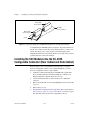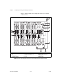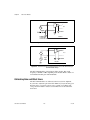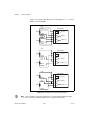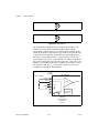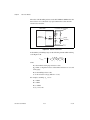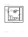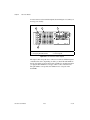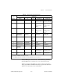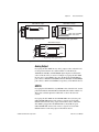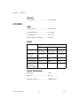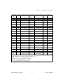
1
Signal Conditioning SCC Series User Manual SCC Series User Manual September 2000 Edition Part Number 321331E-01 Worldwide Technical Support and Product Information ni.com National Instruments Corporate Headquarters 11500 North Mopac Expressway Austin, Texas 78759-3504 USA Tel: 512 794 0100 Worldwide Offices Australia 03 9879 5166, Austria 0662 45 79 90 0, Belgium 02 757 00 20, Brazil 011 284 5011, Canada (Calgary) 403 274 9391, Canada (Ontario) 905 785 0085, Canada (Québec) 514 694 8521, China 0755 3904939, Denmark 45 76 26 00, Finland 09 725 725 11, France 01 48 14 24 24, Germany 089 741 31 30, Greece 30 1 42 96 427, Hong Kong 2645 3186, India 91805275406, Israel 03 6120092, Italy 02 413091, Japan 03 5472 2970, Korea 02 596 7456, Mexico (D.F.) 5 280 7625, Mexico (Monterrey) 8 357 7695, Netherlands 0348 433466, New Zealand 09 914 0488, Norway 32 27 73 00, Poland 0 22 528 94 06, Portugal 351 1 726 9011, Singapore 2265886, Spain 91 640 0085, Sweden 08 587 895 00, Switzerland 056 200 51 51, Taiwan 02 2528 7227, United Kingdom 01635 523545 For further support information, see the Technical Support Resources appendix. To comment on the documentation, send e-mail to [email protected] © Copyright 1997, 2000 National Instruments Corporation. All rights reserved. Important Information Warranty The SC-2345 and SCC Series components are warranted against defects in materials and workmanship for a period of one year from the date of shipment, as evidenced by receipts or other documentation. National Instruments will, at its option, repair or replace equipment that proves to be defective during the warranty period. This warranty includes parts and labor. The media on which you receive National Instruments software are warranted not to fail to execute programming instructions, due to defects in materials and workmanship, for a period of 90 days from date of shipment, as evidenced by receipts or other documentation. National Instruments will, at its option, repair or replace software media that do not execute programming instructions if National Instruments receives notice of such defects during the warranty period. National Instruments does not warrant that the operation of the software shall be uninterrupted or error free. A Return Material Authorization (RMA) number must be obtained from the factory and clearly marked on the outside of the package before any equipment will be accepted for warranty work. National Instruments will pay the shipping costs of returning to the owner parts which are covered by warranty. National Instruments believes that the information in this document is accurate. The document has been carefully reviewed for technical accuracy. In the event that technical or typographical errors exist, National Instruments reserves the right to make changes to subsequent editions of this document without prior notice to holders of this edition. The reader should consult National Instruments if errors are suspected. In no event shall National Instruments be liable for any damages arising out of or related to this document or the information contained in it. EXCEPT AS SPECIFIED HEREIN, NATIONAL INSTRUMENTS MAKES NO WARRANTIES, EXPRESS OR IMPLIED, AND SPECIFICALLY DISCLAIMS ANY WARRANTY OF MERCHANTABILITY OR FITNESS FOR A PARTICULAR PURPOSE. CUSTOMER’S RIGHT TO RECOVER DAMAGES CAUSED BY FAULT OR NEGLIGENCE ON THE PART OF NATIONAL INSTRUMENTS SHALL BE LIMITED TO THE AMOUNT THERETOFORE PAID BY THE CUSTOMER. NATIONAL INSTRUMENTS WILL NOT BE LIABLE FOR DAMAGES RESULTING FROM LOSS OF DATA, PROFITS, USE OF PRODUCTS, OR INCIDENTAL OR CONSEQUENTIAL DAMAGES, EVEN IF ADVISED OF THE POSSIBILITY THEREOF. This limitation of the liability of National Instruments will apply regardless of the form of action, whether in contract or tort, including negligence. Any action against National Instruments must be brought within one year after the cause of action accrues. National Instruments shall not be liable for any delay in performance due to causes beyond its reasonable control. The warranty provided herein does not cover damages, defects, malfunctions, or service failures caused by owner’s failure to follow the National Instruments installation, operation, or maintenance instructions; owner’s modification of the product; owner’s abuse, misuse, or negligent acts; and power failure or surges, fire, flood, accident, actions of third parties, or other events outside reasonable control. Copyright Under the copyright laws, this publication may not be reproduced or transmitted in any form, electronic or mechanical, including photocopying, recording, storing in an information retrieval system, or translating, in whole or in part, without the prior written consent of National Instruments Corporation. Trademarks CVI™, LabVIEW™, National Instruments™, ni.com™, and NI-DAQ™ are trademarks of National Instruments Corporation. ICP® is a registered trademark of PCB Piezotronics, Inc. Other product and company names mentioned herein are trademarks or trade names of their respective companies. WARNING REGARDING USE OF NATIONAL INSTRUMENTS PRODUCTS (1) NATIONAL INSTRUMENTS PRODUCTS ARE NOT DESIGNED WITH COMPONENTS AND TESTING FOR A LEVEL OF RELIABILITY SUITABLE FOR USE IN OR IN CONNECTION WITH SURGICAL IMPLANTS OR AS CRITICAL COMPONENTS IN ANY LIFE SUPPORT SYSTEMS WHOSE FAILURE TO PERFORM CAN REASONABLY BE EXPECTED TO CAUSE SIGNIFICANT INJURY TO A HUMAN. (2) IN ANY APPLICATION, INCLUDING THE ABOVE, RELIABILITY OF OPERATION OF THE SOFTWARE PRODUCTS CAN BE IMPAIRED BY ADVERSE FACTORS, INCLUDING BUT NOT LIMITED TO FLUCTUATIONS IN ELECTRICAL POWER SUPPLY, COMPUTER HARDWARE MALFUNCTIONS, COMPUTER OPERATING SYSTEM SOFTWARE FITNESS, FITNESS OF COMPILERS AND DEVELOPMENT SOFTWARE USED TO DEVELOP AN APPLICATION, INSTALLATION ERRORS, SOFTWARE AND HARDWARE COMPATIBILITY PROBLEMS, MALFUNCTIONS OR FAILURES OF ELECTRONIC MONITORING OR CONTROL DEVICES, TRANSIENT FAILURES OF ELECTRONIC SYSTEMS (HARDWARE AND/OR SOFTWARE), UNANTICIPATED USES OR MISUSES, OR ERRORS ON THE PART OF THE USER OR APPLICATIONS DESIGNER (ADVERSE FACTORS SUCH AS THESE ARE HEREAFTER COLLECTIVELY TERMED “SYSTEM FAILURES”). ANY APPLICATION WHERE A SYSTEM FAILURE WOULD CREATE A RISK OF HARM TO PROPERTY OR PERSONS (INCLUDING THE RISK OF BODILY INJURY AND DEATH) SHOULD NOT BE RELIANT SOLELY UPON ONE FORM OF ELECTRONIC SYSTEM DUE TO THE RISK OF SYSTEM FAILURE. TO AVOID DAMAGE, INJURY, OR DEATH, THE USER OR APPLICATION DESIGNER MUST TAKE REASONABLY PRUDENT STEPS TO PROTECT AGAINST SYSTEM FAILURES, INCLUDING BUT NOT LIMITED TO BACK-UP OR SHUT DOWN MECHANISMS. BECAUSE EACH END-USER SYSTEM IS CUSTOMIZED AND DIFFERS FROM NATIONAL INSTRUMENTS' TESTING PLATFORMS AND BECAUSE A USER OR APPLICATION DESIGNER MAY USE NATIONAL INSTRUMENTS PRODUCTS IN COMBINATION WITH OTHER PRODUCTS IN A MANNER NOT EVALUATED OR CONTEMPLATED BY NATIONAL INSTRUMENTS, THE USER OR APPLICATION DESIGNER IS ULTIMATELY RESPONSIBLE FOR VERIFYING AND VALIDATING THE SUITABILITY OF NATIONAL INSTRUMENTS PRODUCTS WHENEVER NATIONAL INSTRUMENTS PRODUCTS ARE INCORPORATED IN A SYSTEM OR APPLICATION, INCLUDING, WITHOUT LIMITATION, THE APPROPRIATE DESIGN, PROCESS AND SAFETY LEVEL OF SUCH SYSTEM OR APPLICATION. Conventions The following conventions are used in this manual: <> Angle brackets that contain numbers separated by an ellipsis represent a range of values associated with a bit or signal name—for example, DBIO<3..0>. ♦ The ♦ symbol indicates that the following text applies only to a specific product, a specific operating system, or a specific software version. This icon to the left of bold italicized text denotes a note, which alerts you to important information. This icon to the left of bold italicized text denotes a caution, which advises you of precautions to take to avoid injury, data loss, or a system crash. italic Italic text denotes variables, emphasis, a cross reference, or an introduction to a key concept. This font also denotes text that is a placeholder for a word or value that you must supply. SCC SCC refers to an SCC Series signal conditioning module unless otherwise noted. SC-2345 connector block SC-2345 connector block refers to the SC-2345 signal conditioning connector block with a strain relief. SC-2345 configurable connector SC-2345 configurable connector refers to the SC-2345 signal conditioner with either rear cable connections or side cable connections. SC-2345 SC-2345 refers to both the SC-2345 connector block and configurable connector. Contents Chapter 1 Introduction About the SC-2345 and SCC Modules ..........................................................................1-2 What You Need to Get Started ......................................................................................1-3 Unpacking ......................................................................................................................1-4 Installing NI-DAQ and Your DAQ Device ...................................................................1-4 Configuration...................................................................................................1-5 Chapter 2 SCC-PWR Modules Safety Information .........................................................................................................2-3 SCC-PWR01 ..................................................................................................................2-4 SCC-PWR02 ..................................................................................................................2-5 SCC-PWR03 ..................................................................................................................2-5 Chapter 3 Configuring, Connecting, and Installing the SCC Modules Configuring and Connecting the SCC Modules ............................................................3-1 Analog Input SCC Modules ............................................................................3-2 DIO SCC Modules ..........................................................................................3-3 Analog Output SCC Modules..........................................................................3-3 GPCTR SCC Modules.....................................................................................3-3 SCC Signal Connections .................................................................................3-3 Terminal Block Signal Connections................................................................3-4 Installing the SCC Modules into the SC-2345 Connector Block ..................................3-5 Installing the SCC Modules into the SC-2345 Configurable Connector (Rear Cabled and Side Cabled)...................................................................................3-10 I/O Panelette Labels ........................................................................................3-16 Mounting Options............................................................................................3-16 Chapter 4 SCC Series Modules SCC-A10 Voltage Attenuator Module (Buffered).........................................................4-2 Measurement Scaling Considerations .............................................................4-3 SCC-AI Series Isolated Analog Input Modules.............................................................4-3 Calibrating Gain and Offset Errors..................................................................4-6 Measurement Scaling Considerations .............................................................4-8 © National Instruments Corporation v SCC Series User Manual Contents SCC-CI20 Current Input Module (Buffered) ................................................................ 4-8 Input Resistor Replacement ............................................................................ 4-10 Measurement Conversion Considerations ...................................................... 4-11 SCC-ICP01 Integrated Circuit Piezoelectric Input Module .......................................... 4-11 Signal Connections ......................................................................................... 4-12 Measurement Conversion Considerations ...................................................... 4-13 System Accuracy............................................................................................. 4-13 SCC-LP Lowpass Filter Module ................................................................................... 4-14 SCC-LP Performance...................................................................................... 4-14 Using the SCC-LP as an Antialiasing Filter ................................................... 4-19 Signal Connections ......................................................................................... 4-20 Calibrating Gain Errors ................................................................................... 4-21 System Accuracy............................................................................................. 4-22 Measurement Scaling Considerations ............................................................. 4-22 SCC-RTD01 Resistance-Temperature Detector Input Module..................................... 4-23 Signal Connections ......................................................................................... 4-24 Measurement Conversion Considerations ...................................................... 4-27 SCC-SG Series Strain-Gauge Modules ......................................................................... 4-29 Strain Gauge Signal Connections ................................................................... 4-29 SCC-SG01 and SCC-SG02 Quarter-Bridge Connection.................. 4-29 SCC-SG03 Half-Bridge Connection ................................................ 4-31 SCC-SG04 Full-Bridge Connection ................................................. 4-32 Excitation ........................................................................................................ 4-32 Offset Nulling Adjustment.............................................................................. 4-33 Nulling Range Adjustment.............................................................................. 4-33 Filtering ........................................................................................................... 4-35 Shunt Calibration ............................................................................................ 4-35 Measurement Scaling Considerations ............................................................. 4-39 SCC-TC Thermocouple Input Modules ........................................................................ 4-40 Cold-Junction Sensor Output and Accuracy ................................................... 4-43 Open-Thermocouple Detection....................................................................... 4-44 Errors Due to Open-Thermocouple Detection Circuitry .................. 4-44 Calibrating System Offsets ............................................................................. 4-45 Calibrating Your System Using a Thermocouple Calibrator ........... 4-45 Measurement Conversion Considerations ...................................................... 4-46 SCC-FT01 Feedthrough Module................................................................................... 4-47 Signal Connections ......................................................................................... 4-48 Customizing the SCC-FT01............................................................................ 4-49 Circuit Design ................................................................................................. 4-49 Wiring Considerations .................................................................................... 4-52 Analog Input and Digital Input/Output ............................................ 4-52 Analog Output .................................................................................. 4-53 GPCTR ............................................................................................. 4-53 Screw Terminal Connection ............................................................. 4-54 SCC Series User Manual vi ni.com Contents SCC-DI01 Isolated Digital Input Module......................................................................4-54 Signal Connections..........................................................................................4-55 Status LED.......................................................................................................4-55 Sensing DC Voltages.......................................................................................4-55 Sensing AC Voltages.......................................................................................4-56 Signal Isolation................................................................................................4-56 Power-On Condition........................................................................................4-56 SCC-DO01 Isolated Digital Output Module .................................................................4-56 Signal Connections..........................................................................................4-57 Status LED.......................................................................................................4-58 Signal Isolation................................................................................................4-58 Power-On Condition........................................................................................4-58 Appendix A Specifications Appendix B SCC Feature Reference Table Appendix C SCC I/O Connector Pin Information Appendix D Technical Support Resources Glossary Index Figures Figure 2-1. SCC-PWR Parts Locator Diagram ........................................................2-2 Figure 3-1. Figure 3-2. Figure 3-3. Figure 3-4. SCC Socket Configurations and Color Codes.......................................3-2 Two-Part Screw Terminal System ........................................................3-4 Terminal Block I/O Connector Pin Assignments..................................3-5 SC-2345 Connector Block Module Assembly Parts Locator Diagram....................................................................................3-7 SC-2345 Connector Block Board Parts Locator Diagram ....................3-8 Figure 3-5. © National Instruments Corporation vii SCC Series User Manual Contents Figure 3-6. Figure 3-7. Figure 3-8. Figure 3-9. Figure 3-10. Figure 3-11. Figure 3-12. Figure 3-13. Figure 3-14. Figure 3-15. Figure 3-16. Figure 4-1. Figure 4-2. Figure 4-3. Figure 4-4. Figure 4-5. Figure 4-6. Figure 4-7. Figure 4-8. Figure 4-9. Figure 4-10. Figure 4-11. Figure 4-12. Figure 4-13. Figure 4-14. Figure 4-15. Figure 4-16. Figure 4-17. Figure 4-18. Figure 4-19. Figure 4-20. Figure 4-21. Figure 4-22. SCC Series User Manual Single-Stage and Dual-Stage Analog Input SCC Configuration for SC-2345 Connector Block .............................................................. 3-9 Single-Stage Analog Input and DIO SCC Configuration for SC-2345 Connector Block .............................................................. 3-10 Opening the SC-2345 Configurable Connector (Rear Cabled) Enclosure ....................................................................... 3-12 Opening the SC-2345 Configurable Connector (Side Cabled) Enclosure ....................................................................... 3-13 SC-2345 Configurable Connector (Rear Cabled) Board Parts Locator Diagram ................................................................................... 3-14 SC-2345 Configurable Connector (Side Cabled) Board Parts Locator Diagram ................................................................................... 3-15 Installing an I/O Panelette Label........................................................... 3-16 Rack-Mount Option .............................................................................. 3-17 Stack-Mount Option.............................................................................. 3-18 Single and Dual-Stage Analog Input SCC Configuration for SC-2345 Configurable Connector ................................................... 3-19 Single-Stage Analog Input and DIO SCC Configuration for SC-2345 Configurable Connector ................................................... 3-20 SCC-A10 Icon....................................................................................... 4-2 SCC-A10 Signal Connections............................................................... 4-3 SCC-AIXX Icon .................................................................................... 4-4 SCC-AIXX Signal Connections ............................................................ 4-5 Floating Signal Connection for the SCC-AIXX .................................... 4-6 Ground-Referenced Signal Connection for the SCC-AIXX with High Common-Mode Voltage ...................................................... 4-6 SCC-CI20 Icon...................................................................................... 4-9 SCC-CI20 Signal Connection ............................................................... 4-9 SCC-CI20 Parts Locator Diagram ........................................................ 4-10 SCC-ICP01 Icon ................................................................................... 4-11 SCC-ICP01 Signal Connections ........................................................... 4-12 SCC-LP Icon ......................................................................................... 4-14 Typical Response Curve SCC-LP01..................................................... 4-15 Typical Response Curve SCC-LP02..................................................... 4-16 Typical Response Curve SCC-LP03..................................................... 4-16 Typical Response Curve SCC-LP04..................................................... 4-17 Theoretical Transfer Characteristics ..................................................... 4-18 Aliasing of an Input Signal with a Frequency of 0.8 Times the Sample Rate .................................................................................... 4-19 SCC-LP Signal Connection .................................................................. 4-20 SCC-RTD01 Icon.................................................................................. 4-23 SCC-RTD01 Single-Channel Wiring Diagrams ................................... 4-25 SCC-RTD01 Two-Channel Wiring Diagrams...................................... 4-26 viii ni.com Contents Figure 4-23. Figure 4-24. Figure 4-25. Figure 4-26. Figure 4-27. Figure 4-28. Figure 4-29. Figure 4-30. Figure 4-31. Figure 4-32. Figure 4-33. Figure 4-34. Figure 4-35. Figure 4-36. Figure 4-37. Figure 4-38. Figure 4-39. Figure 4-40. Figure 4-41. Figure 4-42. Figure 4-43. SCC-SG01 Icon.....................................................................................4-30 SCC-SG02 Icon.....................................................................................4-30 SCC-SG01/02 Quarter-Bridge Connection ...........................................4-30 SCC-SG03 Icon.....................................................................................4-31 SCC-SG03 Half-Bridge Connection .....................................................4-31 SCC-SG04 Icon.....................................................................................4-32 SCC-SG04 Full-Bridge Connection......................................................4-32 SCC-SG11 Connection..........................................................................4-34 SCC-SG11 Icon.....................................................................................4-35 Dual-Stage Analog Input Configuration for SCC-SG0X and SCC-SG11 Installed in an SC-2345 ...............................................4-36 SCC-SG11 Connection..........................................................................4-37 SCC-TC Icon.........................................................................................4-40 SCC-TC Signal Connection ..................................................................4-42 Thermocouple Calibration Configuration .............................................4-45 SCC-FT01 Icon .....................................................................................4-47 SC-FT01 Parts Locator Diagram...........................................................4-50 SCC-FT01 Prototyping Module Analog Input Configurations.............4-53 SCC-DI01 Icon......................................................................................4-54 SCC-DI01 Signal Connections..............................................................4-55 SCC-DO01 Icon ....................................................................................4-57 SCC-DO01 Signal Connections ............................................................4-57 Figure A-1. Figure A-2. Maximum Sinking Characteristics ........................................................A-25 Maximum Sourcing Characteristics ......................................................A-26 Figure C-1. SCC Module Bottom View ...................................................................C-1 Tables Table 1-1. Minimum NI-DAQ Version Required ..................................................1-5 Table 2-1. Table 2-2. Power Module Usage ...........................................................................2-1 SCC-PWR01 Power Usage Guide .......................................................2-4 Table 4-1. Table 4-2. Table 4-3. Table 4-4. Table 4-5. SCC-AIXX Module Input/Output Range, Gain, and Bandwidth ..........4-4 SCC-AIXX Input Voltage Requirements...............................................4-7 Callendar-Van Dusen Coefficients for Platinum RTDs ........................4-28 SCC-FT01 Signals.................................................................................4-48 Signals Available by SCC Socket Type ...............................................4-51 Table B-1. Table B-2. Table B-3. Analog Input..........................................................................................B-2 Analog Output .......................................................................................B-3 Digital I/O..............................................................................................B-3 © National Instruments Corporation ix SCC Series User Manual Contents Table B-4. GPCTR.................................................................................................. B-3 Table C-1. SCC Module Pin Signal Connections for A10, AIXX, CI20, DI01, DO01, and FT01 Modules .......................................................... C-2 SCC Module Pin SIgnal Connections for ICP01, LPXX, RTD01, SG0X, SG11, and TCXX Modules ....................................................... C-3 Table C-2. SCC Series User Manual x ni.com 1 Introduction This manual describes the electrical and mechanical aspects of the SC-2345 shielded carriers and the SCC Series modules, and contains information concerning their operation, installation, and configuration. The SC-2345 shielded carriers have one of the following power modules factory installed: • SCC-PWR01 • SCC-PWR02 and PS01 power supply • SCC-PWR03 The SCC Series modules include the following: • SCC-A10 voltage attenuator (buffered) • SCC-AI isolated analog input • SCC-CI20 current input (buffered) • SCC-ICP01 Integrated Circuit Piezoelectric (ICP®) input • SCC-LP lowpass filter • SCC-RTD resistance-temperature detector input • SCC-SG strain-gauge • SCC-TC thermocouple input • SCC-FT01 feedthrough • SCC-DI01 isolated digital input • SCC-DO01 isolated digital output © National Instruments Corporation 1-1 SCC Series User Manual Chapter 1 Introduction About the SC-2345 and SCC Modules This chapter describes the SC-2345 shielded carriers and the SCC Series modules, lists what you need to get started, and explains how to unpack your SC-2345 and SCC Series modules. The SC-2345 connects signals to 68-pin E Series DAQ devices. Combined with the SCC Series modules, the carrier offers easy-to-use signal conditioning options on a per channel basis. The SC-2345 carrier provides 42 screw terminal connections to the E Series DAQ device digital signals. When used with a shielded 68-pin cable, the SC-2345 provides rugged, low-noise signal conditioning. The SC-2345 is available in the following form factors: • SC-2345 connector block • SC-2345 configurable connector with rear cable connection • SC-2345 configurable connector with side cable connection The SC-2345 connector block requires you to pass your input signals through a strain relief. The SC-2345 configurable connectors maximize your I/O flexibility through the use of panelettes. All SC-2345s are portable enclosures for laptop and desktop applications. Purchasing the optional rack-mount or stack-mount accessories allows you to mount the SC-2345 configurable connector to suit your application. The rack-mount option is available for standard 19 in. racks. SCC modules are signal conditioning modules used in an SC-2345 connected to your 68-pin E Series DAQ device. The SCC modules add voltage attenuation, current input, thermocouple input, and 24 V digital input and output functionality to your E Series DAQ device. A feedthrough SCC allows direct connection to the analog input or analog output signals. You can customize this feedthrough module to meet your specific signal conditioning needs by placing your circuitry design inside the feedthrough module. SCC Series User Manual 1-2 ni.com Chapter 1 Introduction What You Need to Get Started To set up and use the SC-2345 and the SCC modules, you need the following items: ❑ SC-2345 with one of the following: – SCC-PWR01 – SCC-PWR02 and the PS01 power supply – SCC-PWR03 and a 7 to 42 VDC power supply ❑ One or more of the following SCC modules: – SCC-A10 – SCC-AI – SCC-CI20 – SCC-ICP01 – SCC-LP – SCC-RTD01 – SCC-SG – SCC-TC – SCC-FT01 – SCC-DI01 – SCC-DO01 ❑ SCC Series User Manual ❑ SC-2345 Quick Reference Label ❑ 68-pin E Series DAQ device, documentation, and 68-pin cable ❑ Flathead screwdriver (supplied) ❑ Number 1 and 2 Phillips-head screwdrivers ❑ Wire insulation strippers ❑ NI-DAQ (current version) for Windows NT/2000/9x Note The Macintosh operating system currently is not supported. © National Instruments Corporation 1-3 SCC Series User Manual Chapter 1 Introduction ♦ SC-2345 configurable connector To use this carrier you need the following items in addition to those previously listed: ❑ Rack-mount kit (optional) ❑ Stack-mount kit (optional) ❑ One or more I/O panelettes and label sheet Unpacking Your shielded carrier is shipped in a cardboard box. The SCC modules are shipped in antistatic packaging to prevent electrostatic damage to the modules. Electrostatic discharge can damage several components on these products. To avoid such damage when you handle the products, take the following precautions: • Ground yourself by using a grounding strap or by touching a grounded object. • Touch the antistatic package to a metal part of your computer chassis before removing the modules from the packaging. • Remove the modules from the packaging and inspect the modules for any sign of damage. Notify National Instruments if the modules appear damaged in any way. Do not install a damaged module into your system. • Never touch the exposed pins of connectors. Installing NI-DAQ and Your DAQ Device Install the NI-DAQ driver software before installing your E Series DAQ device. See the DAQ Quick Start Guide provided with your DAQ device for instructions. The SC-2345 requires NI-DAQ. See Table 1-1 to determine which version of NI-DAQ is required for your application. If you need a newer version of NI-DAQ, go to the ni.com Web site and follow the links Download Software»Drivers and Updates»NI-DAQ to find the version of NI-DAQ required for your application. SCC Series User Manual 1-4 ni.com Chapter 1 Introduction Table 1-1. Minimum NI-DAQ Version Required SCC Module NI-DAQ Version (or later) Required SCC-A10 6.0 SCC-AI 6.6 SCC-CI20 6.0 SCC-ICP 6.8 SCC-LP 6.1 SCC-RTD 6.8 SCC-SG 6.6 SCC-TC 6.0 SCC-FT01 6.0 SCC-DI01 6.1 SCC-DO01 6.1 Configuration Run Measurement & Automation Explorer to configure your SCC system. If you need help during the configuration process, open the Measurement & Automation Help file by selecting Help Topics from the Help menu. Follow these steps to configure your SCC system: 1. Double-click the Measurement & Automation Explorer icon on your desktop. 2. Display the list of devices and interfaces by clicking the + next to the Devices and Interfaces icon. 3. Right-click on the appropriate E Series DAQ device you will connect to and select Properties. 4. Select the Accessory tab. 5. Under Accessory: select SC-2345. 6. Select the Configure button. A new window appears listing the slots (connector reference designators) of the SC-2345. 7. Select the connector of the SC-2345 where you have installed a SCC. © National Instruments Corporation 1-5 SCC Series User Manual Chapter 1 Introduction 8. Click Add and select the SCC you have installed. If the SCC name you have installed does not appear in the list, the SCC is not allowed in that location. If you make a mistake in selection, select the connector and click Remove. 9. Click OK after completing all SCC entries. 10. Click OK to complete the configuring process and close Measurement & Automation Explorer. By configuring the SCC system, NI-DAQ performs the appropriate scaling for each SCC. If you are configuring analog input SCCs, the configuration automatically sets the E Series analog input mode to NRSE. If you are configuring DIO SCCs, the configuration automatically sets individual DIO lines to the appropriate input or output mode. Note After properly configuring the SC-2345 as a DAQ device accessory in Measurement & Automation Explorer, NI-DAQ does the scaling required for each SCC type. Refer to the Measurement Scaling Considerations section of your SCC module, in Chapter 4, SCC Series Modules, for more information. SCC Series User Manual 1-6 ni.com 2 SCC-PWR Modules This chapter describes the SCC-PWR module options, how to select the correct SCC-PWR for your application, and important safety information. The SCC-PWR modules are a required part of the SC-2345 system. Your SC-2345 ships with one of three SCC-PWR modules factory installed. The power module options are: SCC-PWR01, SCC-PWR02, and SCC-PWR03. Each power module supplies digital power (+5 V) and analog power (±15 V) to each SCC module in the SC-2345 carrier. LEDs on the SC-2345 indicate whether the +5 V and ±15 V power supplies are functioning properly. Use Table 2-1 to determine the SCC-PWR module that best suits your needs. Note Appendix B, SCC Feature Reference Table, summarizes the power requirements of all SCC modules. Use this to calculate a power requirement budget for your application. Table 2-1. Power Module Usage Power Module SCC-PWR01 © National Instruments Corporation Power Source Usage Suggestions 5 V from E Series DAQ device Total PA consumption ≤ 1.5 W and total SCC module power consumption within the limits of your E Series DAQ device 5 V from external supply Total PA consumption ≤ 2 W and total SCC module power consumption exceeds the limits of your E Series DAQ device 2-1 SCC Series User Manual Chapter 2 SCC-PWR Modules Table 2-1. Power Module Usage (Continued) Power Module Power Source SCC-PWR02 AC (5 V and ±15 V supplied by included PS01 DC adapter) SCC-PWR01 is insufficient or SCC-PWR03 is insufficient SCC-PWR03 7 to 42 VDC from external supply Total PA consumption ≤ 2 W and external supply is 7 to 42 VDC Usage Suggestions PA = analog power To change your SCC-PWR module, unplug the SCC-PWR module that is no longer needed and plug in the new module. Detailed specifications for all SCC-PWR modules are in Appendix A, Specifications. Figure 2-1 shows the SCC-PWR module parts locator diagram. 2 3 1 1 J1 2 S1 3 Product Name Figure 2-1. SCC-PWR Parts Locator Diagram SCC Series User Manual 2-2 ni.com Chapter 2 SCC-PWR Modules Safety Information The following statements contain important safety information concerning hazardous voltages and terminal blocks. Cautions Do not operate the device in an explosive atmosphere or where there may be flammable gases or fumes. Keep away from live circuits. Do not remove equipment covers or shields unless you are trained to do so. If signal wires are connected to the device, hazardous voltages may exist even when the equipment is turned off. To avoid a shock hazard, do not perform procedures involving cover or shield removal unless you are qualified to do so and disconnect all field power prior to removing covers or shields. Equipment described in this document must be used in an Installation Category II1 environment per IEC 664. This category requires local-level-supply mains-connected installation. Do not operate this equipment in a manner that contradicts the information specified in this document. Misuse of this equipment could result in a shock hazard. Connections, including power signals to ground and vice versa, that exceed any of the maximum signal ratings on the device can create a shock or fire hazard or can damage any or all of the boards connected to the host computer and the device. National Instruments is not liable for any damages or injuries resulting from incorrect signal connections. Connect the signal wires to the screw terminals by fully inserting the stripped end of the wire into the terminals. Tighten the terminals to a torque of 5 to 7 in.-lb. Clean devices and terminal blocks by brushing off light dust with a soft nonmetallic brush. Remove other contaminants with deionized water and a stiff nonmetallic brush. The unit must be completely dry and free from contaminants before returning to service. The chassis ground terminal on your SC-2345 connector block and the electromagnetic interference (EMI) gasket attached to the strain-relief of the SC-2345 connector block are for grounding a floating source (1 mA maximum). Do not use these terminals as safety earth grounds. High voltages are voltages greater than or equal to 30 Vrms and 42.4 Vpeak, or 60 VDC in normal conditions and are deemed to be a shock hazard. 1 Category II refers to local-level power distribution, such as that provided by a standard wall outlet. © National Instruments Corporation 2-3 SCC Series User Manual Chapter 2 SCC-PWR Modules SCC-PWR01 The SCC-PWR01 converts +5 V to ±15 V, which is the analog power supply the SCC modules use. Set switch S1 on the SCC-PWR01 to select the source of the +5 V as either external or from the E Series DAQ device. If you select E Series, the SCC-PWR01 uses +5 V power from your E Series DAQ device. If you select external, you must connect a +5 V supply to the screw terminals of J1 on the SCC. Each screw terminal is labeled +5V or GND and should be wired accordingly. See Table 2-2 for usage information for your type of E Series device. Table 2-2. SCC-PWR01 Power Usage Guide Power Source or Device Power Available or Required Supported Configurations AT/PCI E Series PXI DAQPad-6020E DAQPad-6070E 2.4 W available Up to 12 low-power SCC modules or [PA required ≤ 1.5 W and PD required ≤ 2.4 W – (PA / 0.62)] DAQCard DAQPad-MIO-16XE-50 1.14 W available Up to 6 low-power SCC modules or [PA required ≤ 0.72 W and PD required ≤ 1.14 W – (PA / 0.62)] External +5 VDC Power required = (PA / 0.62) + PD Up to 16 low-power SCC modules or total PA required ≤ 2 W PA = total analog power PD = total digital power When PA exceeds the above limits, you must use SCC-PWR02. Note: The efficiency of the +5 V to analog power converter used on the SCC-PWR01 is 62%. The power available is based on the +5 V fuse rating of the E Series DAQ device. SCC Series User Manual 2-4 ni.com Chapter 2 SCC-PWR Modules SCC-PWR02 The SCC-PWR02 is a two-part system that consists of a desktop power supply (PS01) and a filtering component (SCC-PWR02). The PS01 is a 15 W switching supply powered by 90 to 264 VAC (50/60 Hz 1.0 A). To install the PS01, plug the six-position connector of the PS01 into connector J25 of the SC-2345. See Figure 3-5 for the location of connector J25. The SCC-PWR02 filtering component filters and passes on +5 V and ±15 V. The SCC-PWR02 provides sufficient power for most SC-2345 configurations. Refer to Appendix A, Specifications, for details. SCC-PWR03 The SCC-PWR03 converts an external voltage of 7 to 42 VDC to +5 V and ±15 V and requires an external DC power source. Attach your voltage source to the screw terminals of J1. Each screw terminal is labeled 7–42 V or GND and should be wired accordingly. You can power the SCC-PWR03 with any 7 to 42 VDC source such as a standard 12 V car battery. The external power required is calculated as follows: (total PA required / 46.5%) + (total PD / 75%) The two supported configurations are as follows: • Up to 16 low-power SCC modules • Total PA required ≤ 2 W The efficiency of the +5 V step-down converter is 75%. The efficiency of the +5 V-to-analog power converter is 62%. Note © National Instruments Corporation 2-5 SCC Series User Manual 3 Configuring, Connecting, and Installing the SCC Modules This chapter explains how to configure, connect, and install the SCC system. Configuring and Connecting the SCC Modules SCC modules connect to the SC-2345 internal sockets to provide custom signal conditioning options for analog input, analog output, digital input/output (DIO), and general-purpose counter/timers (GPCTRs). The SC-2345 Quick Reference Label illustrates the possible configurations of the SCC modules and defines the location of each signal on the terminal blocks. The numbers on the label correspond to the pin numbers on the 68-pin E Series connector. You can apply the self-adhesive label to the inside cover of the SC-2345. The SCC modules and sockets are keyed for proper orientation and are color-coded for easy connections. All SCC modules have a color stripe across the top that indicates its function classification. The SCC modules fit easily into the correct sockets when properly oriented. Never force an SCC into a socket. Figure 3-1 illustrates the configurations options of the SCC modules on the SC-2345 and shows the color code identification information. The upper section of the figure shows a portion of the SC-2345 Quick Reference Label with a color designation legend under it. © National Instruments Corporation 3-1 SCC Series User Manual Chapter 3 Configuring, Connecting, and Installing the SCC Modules Dual-Stage Analog Input J1-8 J9-16 Single-Stage Analog Input and/or Digital I/O 2nd Stage Analog Input Socket 1st Stage Analog Input Socket Analog Output and/or GPCTR J1-8 Analog Input Single Stage Socket (Optional) J17-18 J9-16 Digital I/O Socket (Optional) J19-20 Analog Output Socket* (Optional) General-Purpose Counter/Timer Socket (Optional) *Analog Output is not available on AI E Series boards Legend: Blue Green Red Yellow Figure 3-1. SCC Socket Configurations and Color Codes SCC modules are required for connecting to the analog inputs or analog outputs of your E Series device. You do not need to go through SCC modules to connect to the GPCTR and the DIO signals of the E Series device. GPCTR and DIO signals are accessible at the SC-2345 terminal block. See the Terminal Block Signal Connections section later in this chapter for details. Analog Input SCC Modules Each analog input SCC label has a blue stripe for easy identification. You can condition analog input signals in two ways: single-stage or dual-stage (cascading) conditioning. For single-stage input conditioning, plug your SCC modules into sockets J1 to J8 and wire the SCC to your I/O signals. For dual-stage analog input conditioning, plug the first-stage SCC into sockets J9 to J16 and plug the second-stage SCC into sockets J1 to J8. When using dual-stage analog input conditioning, wire the first-stage SCC to your I/O signals. The SC-2345 connects the output signals of the first-stage SCC to the inputs of the second-stage SCC. An example of dual-stage conditioning is a voltage attenuator SCC followed by a lowpass filter SCC. Cascading options will be useful as a wider variety of signal SCC Series User Manual 3-2 ni.com Chapter 3 Configuring, Connecting, and Installing the SCC Modules conditioning modules, such as different types of lowpass filters, become available. Sockets J9 to J16 are also available for DIO conditioning or control. If you installed both an analog input SCC and a DIO SCC into the SC-2345, you must wire each SCC separately. You can use all analog input SCC modules in single-stage analog input configurations. You can use most analog input SCC modules in dual-stage configurations by cascading your SCC modules. Refer to Appendix B, SCC Feature Reference Table, to determine correct configurations of each SCC. DIO SCC Modules Each DIO SCC label has a green stripe for easy identification. You can plug DIO SCC modules into the SC-2345 using sockets J9 to J16. Analog Output SCC Modules Each analog output SCC label has a red stripe for easy identification. You can plug analog output SCC modules into the SC-2345 using sockets J17 and J18. Each socket connects to both analog output channels of the E Series device although identified on the SC-2345 for either channel 0 or channel 1. These designations indicate the primary analog output channel each socket uses. Analog output channel 0 is the primary channel for socket J17. Analog output channel 1 is the primary channel for socket J18. GPCTR SCC Modules Each GPCTR SCC label has a yellow stripe for easy identification. You can plug GPCTR SCC modules into the SC-2345 using sockets J19 and J20. Socket J19 connects to GPCTR channel 0. Socket J20 connects to GPCTR channel 1. SCC Signal Connections After you install the SCC modules, attach your signals to the screw terminals of the SCC modules. Each SCC screw terminal is labeled; wire them accordingly. You can find individual details of signal descriptions and signal connections in Chapter 4, SCC Series Modules. © National Instruments Corporation 3-3 SCC Series User Manual Chapter 3 Configuring, Connecting, and Installing the SCC Modules Each SCC screw terminal is a two-part system, with a fixed receptacle and a removable screw terminal, as shown in Figure 3-2. 1 3 2 1 2 1 SCC Screw Terminal Receptacle 2 Removable Screw Terminal Figure 3-2. Two-Part Screw Terminal System This two-part system simplifies the swapping of similar SCC modules. For example, when using an SCC for filtering on an analog input channel, you can remove the screw terminal from the SCC and plug it into another filtering component with the same pin assignment and you do not need to rewire the screw terminal. Depending on the module and its function, the two-part system has a different number of terminals and different size terminals. For safety, high-voltage input SCC modules contain larger screw terminals and will not connect to low-voltage input SCC screw terminal receptacles. Terminal Block Signal Connections The SC-2345 has a 42-position, triple-row screw terminal block for connection to the E Series digital signals. The terminal block can connect to DIO <0..7>, +5 V, DGND, PFI <0..9>, GPCTR, AISENSE, FREQ_OUT, EXTSTROBE, and SCANCLK. The SC-2345 Quick Reference Label identifies the location of each signal on the terminal rows A to C. The terminal label numbers correspond to the pin number location of each signal on the 68-pin E Series connector. See your E Series device user manual for more information about this connector. SCC Series User Manual 3-4 ni.com Chapter 3 Configuring, Connecting, and Installing the SCC Modules Figure 3-3 shows the location of each signal on the terminal block. A Not Used Not Used FREQ_OUT GPCTR0_OUT PFI8/GPCTR0_SOURCE PFI6/WFTRIG PFI4/GPCTR1_GATE PFI2/CONVERT* PFI0/TRIG1 (+) 5 V DIO6 DIO4 DIO2 DIO0 1 2 37 5 41 43 11 14 16 19 49 52 B Not Used DGND DGND DGND DGND DGND DGND DGND DGND DGND DGND DGND DGND DGND 35 4 36 39 7 9 44 12 13 15 50 18 53 C Not Used AISENSE EXTSTROBE* GPCTR1_OUT PFI9/GPCTR0_GATE PFI7/STARTSCAN PFI5/UPDATE* PFI3/GPCTR1_SOURCE PFI1/TRIG2 SCANCLK DIO7 DIO5 DIO3 DIO1 62 45 40 3 38 6 42 10 46 48 51 47 17 Figure 3-3. Terminal Block I/O Connector Pin Assignments Installing the SCC Modules into the SC-2345 Connector Block Refer to Figure 3-4 as you perform the following steps to set up the SC-2345 connector block: 1. Configure your E Series device in nonreferenced single-ended (NRSE) analog input mode. If you use Measurement & Automation Explorer, configure your E Series with the SC-2345 accessory. 2. Connect the 68-pin E Series cable to the SC-2345 connector block. 3. Remove the cover screws on either side of the top cover with a Number 1 Phillips-head screwdriver. Open the top cover. 4. Loosen the strain-relief screws with a Number 2 Phillips-head screwdriver and slide the signal wires through the strain-relief opening. If you are connecting multiple signals, you may need to remove the top strain-relief bar. 5. Plug the SCC components into the appropriate SCC sockets. Refer to the Configuring and Connecting the SCC Modules section for proper SCC installation into the SC-2345 connector block. © National Instruments Corporation 3-5 SCC Series User Manual Chapter 3 Configuring, Connecting, and Installing the SCC Modules SCC Series User Manual 6. Connect your signal wires to the screw terminals and screw terminal block by stripping off 0.25 in. of insulation, inserting the wires into the screw terminals, and tightening the screws. For complete signal connection information, refer to Chapter 4, SCC Series Modules. 7. Reinstall the strain-relief bar, if necessary, and tighten the strain-relief screws. 8. Close the top cover. 9. Reinsert the grounding screws to ensure proper shielding. 3-6 ni.com Chapter 3 Configuring, Connecting, and Installing the SCC Modules 3 Po ssib le S (Co C lor ind C C ica tes onfi stri ura pe g on tio SC ns C) SC Re -234 fere 5 Q n u P/N1 ce ick Lab 841 14A el 01 Row A 68 Po Term sitio in n E al Se Blo ries ck efi Pin D uNm nitio n Row bers and B am N es Row C 2 1 XX C-X SC XX C-X SC XX C-X SC 4 5 10 6 9 7 8 1 2 3 Screw Terminals SCC Modules Cover Screws 4 5 6 68-Pin E Series Cable Quick Reference Label SCC-PWRXX 7 8 9 SCC Socket 10 Strain-Relief Screws Screw Terminal Block Top Strain-Relief Bar Figure 3-4. SC-2345 Connector Block Module Assembly Parts Locator Diagram © National Instruments Corporation 3-7 SCC Series User Manual Chapter 3 Configuring, Connecting, and Installing the SCC Modules Figure 3-5 is the parts locator diagram for the SC-2345 connector block and shows all SCC socket locations. 3 6 5 J18 J17 J8 J7 J6 J5 J4 J3 J2 J1 2 4 7 8 J20 J19 J16 J15 J14 J13 J12 J11 J10 J9 1 9 10 12 1 2 3 4 SCC Socket SCC Key Slot SCC Socket Reference Designator Serial Number 11 5 6 7 8 9 J24 J25 J21 Power LEDs Screw Terminal Block 10 Grounding Terminal Lug 11 Assembly Number 12 Product Name Figure 3-5. SC-2345 Connector Block Board Parts Locator Diagram SCC Series User Manual 3-8 ni.com Chapter 3 Configuring, Connecting, and Installing the SCC Modules Figures 3-6 and 3-7 show how to install analog input and DIO SCC modules into the SC-2345 connector block. Analog SCC Connected to J1 SC-2345 Connector Block 3 2 1 J9 (SCC Component Not Installed) a. Single-Stage Analog Input Second Stage Analog SCC Connected to J1 First Stage SC-2345 Connector Block 3 2 1 Analog SCC Connected to J9 3 2 1 DO NOT connect any signals to the second stage SCC. b. Dual-Stage Analog Input Second Stage Analog SCC Connected to J1 First Stage INCO Analog SCC Connected to J9 3 2 1 SC-2345 Connector Block 3 2 1 RRE CT c. Incorrect Signal Connections for Dual-Stage Conditioning Figure 3-6. Single-Stage and Dual-Stage Analog Input SCC Configuration for SC-2345 Connector Block © National Instruments Corporation 3-9 SCC Series User Manual Chapter 3 Configuring, Connecting, and Installing the SCC Modules Analog SCC Connected to J1 SC-2345 Connector Block 3 2 1 Digital SCC Connected to J9 3 2 1 Inputs Figure 3-7. Single-Stage Analog Input and DIO SCC Configuration for SC-2345 Connector Block A metallized nylon knit EMI gasket is attached to the strain-relief bars of the SC-2345 connector block. If you use shielded cables to connect your signals, this allows you to easily ground your shielded signal cables. Stripping the insulation away from the shield of your cables forms a chassis ground connection at the strain-relief bar. Installing the SCC Modules into the SC-2345 Configurable Connector (Rear Cabled and Side Cabled) Refer to Figure 3-8 as you perform the following steps to set up the SC-2345 configurable connector (rear cabled) and Figure 3-9 for the SC-2345 configurable connector (side cabled): SCC Series User Manual 1. Configure your E Series DAQ device in NRSE analog input mode. If you use Measurement & Automation Explorer, configure your E Series DAQ device with the SC-2345 accessory. 2. Connect the 68-pin E Series cable to the SC-2345 configurable connector. 3. Remove the eight 4-40 × 1/4 in. flathead Phillips-head screws from the top cover. 4. Remove the top cover. 5. Plug the SCC components into the appropriate SCC sockets. Refer to the Configuring and Connecting the SCC Modules section for proper SCC installation into the SC-2345 configurable connector. 3-10 ni.com Chapter 3 6. 7. Configuring, Connecting, and Installing the SCC Modules Install the I/O panelettes: a. Place the lower edge of the I/O panelette in the groove at the bottom of the enclosure opening. b. Tilt the panelette top back into the enclosure. c. Secure the panelette with either one, two, or three (depending on the type of I/O panelette) M2.5 × 6 panhead screws that are included with the panelette. d. You must remove the pre-installed rear panel prior to installing any I/O panelettes on the rear of the SC-2345 configurable connector. e. Install a blank panelette in any unused panelette opening. Connect your panelette wires to the SCC module screw terminals and screw terminal block by stripping off 0.25 in. of insulation, inserting the wires into the screw terminals, and tightening the screws. For complete signal connection information, refer to Chapter 4, SCC Series Modules. If you want to label your panelletes at this time, see I/O Panelette Labels later in this chapter. Note 8. © National Instruments Corporation Replace the top cover and install the screws. 3-11 SCC Series User Manual Chapter 3 Configuring, Connecting, and Installing the SCC Modules 10 9 8 7 1 6 2 XX C-X SC XX C-X SC CH XX C-X SC 1 CH XX 2 C-X SC 5 3 4 1 2 3 4 68-Pin E Series Cable Strain-Relief Panelette SCC Modules SCC Socket 5 6 7 8 BNC Panelette SCC-PWRXX Screw Terminals Screw Terminal Block 9 Top Cover 10 Cover Screws Figure 3-8. Opening the SC-2345 Configurable Connector (Rear Cabled) Enclosure SCC Series User Manual 3-12 ni.com Chapter 3 Configuring, Connecting, and Installing the SCC Modules 1 2 3 4 5 6 XX C-X SC XX C-X SC CH XX C-X SC XX C-X SC 1 CH 2 10 7 9 8 1 2 3 4 Cover Screws Top Cover Screw Terminals SCC Modules 5 6 7 8 Strain-Relief Panelette Screw Terminal Block 68-Pin E Series Cable SCC-PWRXX 9 BNC Panelette 10 SCC Socket Figure 3-9. Opening the SC-2345 Configurable Connector (Side Cabled) Enclosure © National Instruments Corporation 3-13 SCC Series User Manual Chapter 3 Configuring, Connecting, and Installing the SCC Modules Figure 3-10 shows the SC-2345 configurable connector (rear cabled) socket locations. 1 2 3 4 11 5 10 9 6 8 1 2 3 4 Power LEDs J21 Serial Number Assembly Number 5 6 7 8 Product Name Screw Terminal Block J25 J24 7 9 SCC Key Slot 10 SCC Socket Reference Designator 11 SCC Socket Figure 3-10. SC-2345 Configurable Connector (Rear Cabled) Board Parts Locator Diagram SCC Series User Manual 3-14 ni.com Chapter 3 Configuring, Connecting, and Installing the SCC Modules Figure 3-11 shows the SC-2345 configurable connector (side cabled) socket locations. 4 5 6 7 3 8 2 1 9 10 11 1 2 3 4 SCC Socket SCC Key Slot SCC Socket Reference Designator Screw Terminal Block 5 6 7 8 Product Name Assembly Number Serial Number J24 9 Power LEDs 10 J25 11 J21 Figure 3-11. SC-2345 Configurable Connector (Side Cabled) Board Parts Locator Diagram © National Instruments Corporation 3-15 SCC Series User Manual Chapter 3 Configuring, Connecting, and Installing the SCC Modules I/O Panelette Labels Each SC-2345 configurable connector enclosure ships with a sheet of labels for you to apply to your I/O panelettes (see Figure 3-12). The label sheet has both preprinted and blank labels. You can customize the blank labels to suit your application. You can use two labels on single-width I/O panelettes and three or more labels on wider panelettes. 2 1 1 I/O Panelette 2 Label Figure 3-12. Installing an I/O Panelette Label Mounting Options To use your SC-2345 configurable connector enclosure in a standard 19 in. rack-mount configuration install the optional CA-1000 rack-mount kit. To use your SC-2345 configurable connector enclosure in a desktop stacking configuration install the optional CA-1000 stack-mount kit. Refer to Figure 3-13 and use the following steps to install the CA-1000 rack-mount kit on your SC-2345 configurable connector enclosure: 1. Attach a rack-mount bracket to one end of the enclosure with two 4-40 × 1/4 in. screws from the rack-mount kit. 2. Attach a rack-mount bracket to the other end of the enclosure with two 4-40 × 1/4 in. screws from the rack-mount kit. You must remove the rubber feet from the bottom of the SC-2345 enclosure for use in rack-mount applications. Note SCC Series User Manual 3-16 ni.com Chapter 3 Configuring, Connecting, and Installing the SCC Modules 1 2 1 2 1 4-40 x 1/4 in. Screws 2 Rack-Mount Brackets Figure 3-13. Rack-Mount Option Refer to Figure 3-14 and use the following steps to install the CA-1000 stack-mount kit on your SC-2345 configurable connector enclosure: 1. Attach the stack-mount brackets to both ends of the lower enclosure with the 4-40 × 1/4 in. flathead screws from the stack-mount kit. 2. Place the upper enclosure on top of the lower enclosure. 3. Attach the stack-mount brackets to both ends of the upper enclosure with the 4-40 × 1/4 in. flathead screws from the stack-mount kit. You must remove the rubber feet from all but the bottom enclosure before stacking the enclosures. Note © National Instruments Corporation 3-17 SCC Series User Manual Chapter 3 Configuring, Connecting, and Installing the SCC Modules 1 2 1 1 2 1 1 4-40 × 1/4 in. Screws 2 Stack-Mount Brackets Figure 3-14. Stack-Mount Option You can stack additional enclosures by using additional stack-mount kits. You can remove the stack-mount kit handles, if necessary, by removing the two screws that attach the handle. SCC Series User Manual 3-18 ni.com Chapter 3 Configuring, Connecting, and Installing the SCC Modules Figures 3-15 and 3-16 show how to install analog input and DIO SCC modules into the SC-2345 configurable connector. J9 (SCC Component Not Installed) SC-2345 Configurable Connector Analog SCC Connected to J1 3 2 1 a. Single-Stage Analog Input First Stage Analog SCC Connected to J9 Second Stage SC-2345 Configurable Connector 3 2 1 Analog SCC Connected to J1 3 2 1 DO NOT connect any signals to the second stage SCC. b. Dual-Stage Analog Input Analog SCC Connected to J9 First Stage Second Stage INCO RRE SC-2345 Configurable Connector Analog SCC Connected to J1 CT 3 2 1 c. Incorrect Signal Connections for Dual-Stage Conditioning Figure 3-15. Single and Dual-Stage Analog Input SCC Configuration for SC-2345 Configurable Connector © National Instruments Corporation 3-19 SCC Series User Manual Chapter 3 Configuring, Connecting, and Installing the SCC Modules 2 1 3 5 3 2 1 4 1 2 Digital SCC Connected to J9 Inputs 3 SC-2345 Configurable Connector 4 5 Inputs Analog SCC Connected to J1 Figure 3-16. Single-Stage Analog Input and DIO SCC Configuration for SC-2345 Configurable Connector SCC Series User Manual 3-20 ni.com SCC Series Modules 4 This chapter describes signal conditioning modules for the SC-2345 carriers. The SCC Series modules include the following: • SCC-A10 voltage attenuator (buffered) • SCC-AI isolated analog input • SCC-CI20 current input (buffered) • SCC-ICP integrated circuit piezoelectric input • SCC-LP lowpass filter • SCC-RTD01 resistance-temperature detector input • SCC-SG strain-gauge • SCC-TC thermocouple input • SCC-FT01 feedthrough • SCC-DI01 isolated digital input • SCC-DO01 isolated digital output See Appendix B, SCC Feature Reference Table, to calculate the power requirements for your SCC modules. © National Instruments Corporation 4-1 SCC Series User Manual Chapter 4 SCC Series Modules SCC-A10 Voltage Attenuator Module (Buffered) The SCC-A10 voltage attenuator accepts up to two voltage sources at a maximum of 100 V, attenuates each source by a factor of 10, and provides a differential measurement of the source. A differential instrumentation amplifier buffers the input signals allowing maximum scan rates by the E Series device. The SCC-A10 contains circuitry capable of protecting E Series devices for input signals up to 250 Vrms. A blue label stripe identifies the SCC-A10 as an analog input module. Figure 4-1 shows the icon that represents the SCC-A10. Figure 4-1. SCC-A10 Icon You can plug the SCC-A10 into any analog input socket on the SC-2345, although the module cannot function as the second stage of a dual-stage configuration. The SCC-A10 has two differential analog input channels that can measure signals of up to 100 V. Pins 1 and 2 form a differential channel that is routed to E Series device channel X+8, where X+8 is channel 8 through 15 depending on the socket where you plug the SCC-A10. Pins 3 and 4 form the second differential channel that is routed to E Series device channel X, where X is channel 0 through 7 depending on the socket where you plug the SCC-A10. Your signal source can be floating or ground-referenced. Floating signal sources do not require bias resistors to ground with the SCC-A10. The SCC-A10 design does not require high-impedance bias resistors for floating sources. Figure 4-2 shows the SCC-A10 signal connections. SCC Series User Manual 4-2 ni.com Chapter 4 Signal Source SCC Series Modules SCC-A10 4 E Series Device Overvoltage Protection + – + – 3 CH(x) Overvoltage Protection AISENSE 2 AIGND Overvoltage Protection + – + – 1 CH(x+8) Overvoltage Protection Signal source may be floating or ground-referenced. Figure 4-2. SCC-A10 Signal Connections Measurement Scaling Considerations In your software environment if you configured the SCC-A10 using Measurement & Automation Explorer and you are using NI-DAQ software calls, the voltage reading you get from the E Series DAQ device will account for the voltage scaling effect of the SCC-A10. Otherwise, since the voltage measurement from the E Series DAQ device is one-tenth of the voltage applied at the SCC-A10 input, you must multiply the voltage reading you got from the E Series DAQ device by 10 to get the correct input voltage. SCC-AI Series Isolated Analog Input Modules The SCC-AIXX isolated input modules fulfill two purposes. The first purpose is to convert a signal with high common-mode voltage into a single-ended signal referenced to the E Series device AI ground. After this conversion, you can extract the input signal from a high common-mode voltage before it is sampled by the E Series device. The second purpose of the SCC-AIXX isolated input modules is to amplify and filter the input signals, resulting in higher measurement resolution and accuracy. The gain and bandwidth for each module are given in Table 4-1. © National Instruments Corporation 4-3 SCC Series User Manual Chapter 4 SCC Series Modules The SCC-AIXX is safe for use with transients associated with local level main supplies of up to 300 V Installation Category (over-voltage category) II. Category II 300 V local level main supplies can see occasional transients of up to 1500 V. In compliance with IEC/EN 61010-1, UL 3111-1, and CSA/CAN C22.2 No. 1010.1 safety standards, all SCC modules are factory tested at 2300 V, input to output, to ensure that the safety insulation remains intact. Note Table 4-1. SCC-AIXX Module Input/Output Range, Gain, and Bandwidth Model Input Range Output Range Gain Bandwidth SCC-AI01 ±42 V ±8.4 V 0.2 10 kHz SCC-AI02 ±20 V ±10 V 0.5 10 kHz SCC-AI03 ±10 V ±10 V 1 10 kHz SCC-AI04 ±5 V ±10 V 2 10 kHz SCC-AI05 ±1 V ±10 V 10 10 kHz SCC-AI06 ±100 mV ±10 V 100 10 kHz SCC-AI07 ±50 mV ±10 V 200 10 kHz SCC-AI13 ±10 V ±10 V 1 4 Hz SCC-AI14 ±5 V ±10 V 2 4 Hz A blue label stripe identifies the SCC-AIXX as an analog input module. Figure 4-3 shows the icon that represents the SCC-AIXX modules. Figure 4-3. SCC-AIXX Icon You can plug the SCC-AIXX into any analog input socket on the SC-2345, although the module cannot function as the second stage of a dual-stage configuration. Each SCC-AIXX module has two isolated, single-ended analog input channels for measuring signals within the ranges given in Table 4-1. SCC Series User Manual 4-4 ni.com Chapter 4 SCC Series Modules Pins 1 and 2 form a channel that is routed to the E Series device channel X+8, where X+8 is channel 8 through 15 depending on the socket where you place the SCC-AIXX. Pins 3 and 4 form a channel that is routed to E Series device channel X, where X is 0 through 7 depending on the socket where you place the SCC-AIXX. These modules provide channel-to-ground isolation only. They do not provide channel-to-channel isolation. Since both channels must have the same reference voltage, pins 1 and 3 are internally connected together. Figure 4-4 shows the SCC-AIXX signal connections. Signal Source E Series Device SCC-AIXX 4 + + – Lowpass Filter 3 CH(X ) – AISENSE AIGND 2 + + – Lowpass Filter 1 CH(X +8) – Figure 4-4. SCC-AIXX Signal Connections The inputs are designed in a floating single-ended configuration. You can safely reference the measured voltage to a ground level with working common-mode voltage up to 300 V in a Category II installation. If a high common mode voltage is present, connect the negative input pins, pins 1 and 3, to this signal reference. If the measured signals are floating, connect the negative input pins, pins 1 and 3, to AISENSE on the SC-2345 terminal block with a 10 kΩ to 100 kΩ resistor, as shown in Figure 4-5. AISENSE is located on the SC-2345 terminal block, shown in Figures 3-5, 3-10, and 3-11. Figure 4-6 shows how to connect a ground referenced signal to the SCC-AIXX. © National Instruments Corporation 4-5 SCC Series User Manual Chapter 4 SCC Series Modules + + + Vs Vout – – AIGND I AISENSE on SC-2345 terminal block Module Figure 4-5. Floating Signal Connection for the SCC-AIXX + + Vs + Vout – – + Vcm High – CMV I AIGND Module Figure 4-6. Ground-Referenced Signal Connection for the SCC-AIXX with High Common-Mode Voltage The SCC-AIXX modules contain lowpass filter circuitry. The cutoff frequency is 10 kHz or 4 Hz, depending on the module. Refer to Table 4-1 for individual module gains and bandwidths. Calibrating Gain and Offset Errors The SCC-AIXX modules are calibrated at the factory before shipment. If you want to adjust the gain of the SCC-AIXX in your system using your E Series device, you need a voltage source capable of providing a DC voltage shown in Table 4-2 that is several times more accurate than the SCC itself. SCC Series User Manual 4-6 ni.com Chapter 4 SCC Series Modules Table 4-2. SCC-AIXX Input Voltage Requirements Module Input Voltage Required SCC-AI01 40 V SCC-AI02 16 V SCC-AI03 8V SCC-AI04 4V SCC-AI05 800 mV SCC-AI06 80 mV SCC-AI07 40 mV SCC-AI13 8V SCC-AI14 4V To adjust the gain of the SCC-AIXX use the following procedure: 1. Select the desired SCC-AIXX channel on the E Series device. 2. Set the gain on the E Series device so that the E Series input range is ±10 V. 3. Connect the voltage source to the screw terminals of your desired channel on the SCC-AIXX. 4. Apply the voltage given in Table 4-2 that corresponds to your SCC-AIXX module. For example, if you have an SCC-AI03, you must apply 8 VDC. 5. Using your software, have the E Series device read the desired channel on the SCC-AIXX and record the value. 6. Input 0 VDC to the SCC-AIXX. 7. Have the E Series device read that channel and record the value. 8. Subtract the values read (first reading – second reading). 9. Adjust the appropriate trimpot protruding through the top of the SCC-AIXX, labeled Gain. 10. Repeat steps 4 through 9 until the difference you got in step 8 equals the Input Voltage Required value shown in Table 4-2—8 V in this example using an SCC-AI03. Note Turn the trimpot clockwise to increase the gain. © National Instruments Corporation 4-7 SCC Series User Manual Chapter 4 SCC Series Modules For example, assume that you have an SCC-AI03 module. You first connect 8 VDC to the input of CH(X). The E Series device reads 8.05 V as the SCC output. You then connect 0 VDC to the input of CH(X) and the E Series device reads –0.01 V as the SCC output. You subtract these readings, 8.05 – (–0.01) = 8.06 getting a difference of 8.06 V. Because this difference is not equal to 8 V, you must adjust the gain trimpot and repeat the procedure until the difference in outputs equals 8 V. In this example there may be an offset voltage such that the final readings are 8.01 V and 0.01 V for a difference of 8 V. The Gain trimpot adjusted in step 9 of the above procedure only adjusts for gain errors and does not compensate for this offset voltage. Note Use the following procedure to adjust the offset voltage of the SCC-AIXX: 1. Select the desired SCC-AIXX channel on the E Series device. 2. Set the gain on the E Series device so that the E Series input range is ±10 V. 3. Connect the screw terminals of your desired channel on the SCC-AIXX together. 4. Using your software, have the E Series device read the channel. 5. If the value read is not equal to 0.00 V, adjust the appropriate trimpot protruding through the top of the SCC-AIXX, labeled Offset. Turning the trimpot clockwise causes the offset to be increased. 6. Repeat steps 4 and 5 until the voltage read in step 4 equals 0.00 V. Measurement Scaling Considerations If you configured the SCC-AIXX using Measurement & Automation Explorer, the voltage reading you get from the E Series DAQ device accounts for the voltage scaling effect of the SCC-AIXX modules. Otherwise, since the voltage measurement from the E Series DAQ device is scaled by the gain given in Table 4-1, you must divide the voltage reading returned by the device by this gain to get the correct input voltage. SCC-CI20 Current Input Module (Buffered) The SCC-CI20 accepts up to two current sources at a maximum of 20 mA. The SCC-CI20 converts the current to voltage using a precision 249 Ω resistor and provides a differential measurement of the source. The E Series device measures voltage as a 0 to +5 V input signal. A differential instrumentation amplifier buffers the input signals allowing maximum scan rates by the E Series device. SCC Series User Manual 4-8 ni.com Chapter 4 SCC Series Modules A blue label stripe identifies the SCC-CI20 as an analog input module. Figure 4-7 shows the icon that represents the SCC-CI20. You can plug the SCC-CI20 into any analog input socket. IIN VOUT Figure 4-7. SCC-CI20 Icon The SCC-CI20 provides two differential analog input channels for 0 to 20 mA signals. Pins 1 and 2 form a differential channel that is routed to E Series device channel X+8, where X+8 is channel 8 through 15 depending on the socket where you plug the SCC-CI20. Pins 3 and 4 form the second differential channel that is routed to E Series channel X, where X is channel 0 through 7 depending on the socket where you plug the SCC-CI20. Figure 4-8 shows the SCC-CI20 signal connections. Signal Source SCC-C120 4 + – E Series Device Overvoltage Protection + – R3 3 CH(x) Overvoltage Protection AISENSE 10 M AIGND 2 + – Overvoltage Protection + – R2 1 CH(x+8) Overvoltage Protection 10 M Signal source may be floating or ground-referenced. Figure 4-8. SCC-CI20 Signal Connection © National Instruments Corporation 4-9 SCC Series User Manual Chapter 4 SCC Series Modules Input Resistor Replacement Your signal source can be floating or ground-referenced. Floating signal sources do not require bias resistors to ground with the SCC-CI20. The SCC-CI20 has high-impedance bias resistors typically required for floating sources. Incorrect connections can damage the input resistors. Spare 249 Ω resistors are available inside the SCC-CI20. To open the SCC-CI20: 1. Remove the screw from the back (wide unlabeled side). 2. Turn the front (wide labeled side) toward you. 3. Place the screw terminal receptacle to the left. 4. Slide the top cover to the right. 5. Lift off the cover. The locations of the spare resistors are illustrated in Figure 4-9. Resistor 2 (R2) and resistor 3 (R3) are socketed for quick and easy replacement. Replace R2 and R3 with the spares when needed. 1 2 3 4 5 1 R3 2 Product Name 3 4 Assembly Number Spare Resistors 5 R2 Figure 4-9. SCC-CI20 Parts Locator Diagram SCC Series User Manual 4-10 ni.com Chapter 4 SCC Series Modules Measurement Conversion Considerations In your software environment if you have configured the SCC-CI20 using Measurement & Automation Explorer and you are using NI-DAQ software calls, the reading you get from the E Series device accounts for the voltage to current conversion and returns milliamps not volts. Otherwise the measurement from the E Series device is a unit of volts; you must convert your voltage measurement to current measurement. To make this conversion, use the following formula: V I = ------------0.249 where I is milliamps and V is volts. SCC-ICP01 Integrated Circuit Piezoelectric Input Module The SCC-ICP01 input module accepts an ICP input signal of analog bandwidth that is less than 5 kHz (recommended). The signal passes through a 0.8 Hz highpass filter, is amplified, and then passes through a 19 kHz lowpass Bessel filter. The output is buffered to allow maximum scan rates. This module has a fixed gain of 2, therefore, the maximum input is ±5 V. The SCC-ICP01 provides a 4 mA current source for ICP excitation. A blue stripe identifies the SCC-ICP01 as an analog input module. Figure 4-10 shows the icon that represents the SCC-ICP01. Figure 4-10. SCC-ICP01 Icon © National Instruments Corporation 4-11 SCC Series User Manual Chapter 4 SCC Series Modules Signal Connections The SCC-ICP01 provides one differential analog input channel for measuring the voltage across the ICP. Pins 1 and 2 form a differential channel that is routed to E Series channel X, where X is channel 0 through 7 depending on the socket into which you plug the SCC-ICP01. Pins 3 and 4 are used for the constant-current excitation source of 4 mA. Figure 4-11 shows the signal connections. SCC-ICP01 4 3 2 1 ICP + – IEX (4 mA) AC Coupling + – 19 kHz Lowpass Bessel CH(X ) Figure 4-11. SCC-ICP01 Signal Connections Notes Your signal source can be floating or ground referenced. The SCC-ICP01 has high impedance bias resistors typically required for floating sources. External bias resistors connected to ground are not required. You can plug the SCC-ICP01 into any analog input socket on the SC-2345. Due to the unique front end circuit required for ICP sensors, this module cannot function as the second stage of a dual-stage configuration. For floating signal sources in high noise environments, connecting the negative terminal of the signal source to the AIGND terminal on the SC-2345 screw terminal block reduces common-mode noise. SCC Series User Manual 4-12 ni.com Chapter 4 SCC Series Modules Measurement Conversion Considerations If you have configured the SCC-ICP01 using Measurement & Automation Explorer and you are using NI-DAQ driver software, the reading you get from the E Series DAQ device is properly scaled. Otherwise you must scale and convert your readings as described below: 1. Measure the ICP voltage. a. Read the ICP channel on the E Series DAQ device VESERIES (CHX). b. Calculate the ICP voltage using this formula: VICP = VESERIES/2 where VICP is the ICP voltage. VESERIES is the E Series DAQ device voltage. Note This step provides proper scaling for the ICP amplifier in the SCC-ICP01. 2. Use scaling constants obtained from your sensor data sheet to convert the ICP voltage to the desired unit such as Newtons, m/s2, or g. System Accuracy The system accuracy is determined by the combined accuracy of the SCC module and the E Series device. SCC modules that are under factory calibration condition have the following system accuracy: System Accuracy = (GEE × Reading) + EE + OES where GEE is gain error as a percent of the reading of the E Series DAQ device. Reading is the measured voltage. EE is the offset voltage error in volts of the E Series DAQ device. OES is the offset error in mV of the SCC module. © National Instruments Corporation 4-13 SCC Series User Manual Chapter 4 SCC Series Modules SCC-LP Lowpass Filter Module The SCC-LP series components are fourth-order Butterworth filter components that accept signals within a ±10 V range. The input signals pass through a differential amplifier providing a differential measurement, attenuated by a factor of two. The output of the amplifier passes through a fourth-order Butterworth filter circuit that is buffered to allow maximum scan rates. The SCC-LP series consists of the following modules: • SCC-LP01—cutoff frequency, 25 Hz • SCC-LP02—cutoff frequency, 50 Hz • SCC-LP03—cutoff frequency, 150 Hz • SCC-LP04—cutoff frequency, 1 kHz A blue label stripe identifies the SCC-LP as an analog input component. Figure 4-12 shows the icon that represents the SCC-LP. You can plug the SCC-LP into any analog input socket. Hz Figure 4-12. SCC-LP Icon SCC-LP Performance The filter used in the SCC-LP series components is a Butterworth filter, and is characterized by maximal flatness in the passband with very sharp monotonic rolloff. It has a nonlinear phase response, the delay is not constant, and the step response exhibits a moderate amount of overshoot (ringing). These characteristics present no problems for amplitude-based applications. SCC Series User Manual 4-14 ni.com Chapter 4 SCC Series Modules The Butterworth filter is a good general-purpose filter. Figures 4-13 through 4-16 show the typical response curve for each SCC-LP. – 5.0 Amplitude (dB) 0.0 – 5.0 – 10.0 – 15.0 – 20.0 – 25.0 1 2 3 4 5 10 20 25 50 Frequency (Hz) Figure 4-13. Typical Response Curve SCC-LP01 © National Instruments Corporation 4-15 SCC Series User Manual Chapter 4 SCC Series Modules 0.0 Amplitude (dB) – 5.0 – 10.0 – 15.0 – 20.0 – 25.0 1 2 3 4 5 10 20 25 50 100 Frequency (Hz) Figure 4-14. Typical Response Curve SCC-LP02 0.0 Amplitude (dB) – 5.0 – 10.0 – 15.0 – 20.0 – 25.0 1 2 3 4 5 10 20 25 50 150 300 Frequency (Hz) Figure 4-15. Typical Response Curve SCC-LP03 SCC Series User Manual 4-16 ni.com Chapter 4 SCC Series Modules 2.5 0.0 Amplitude (dB) –5.0 –10.0 –15.0 –20.0 –25.0 1 2 3 4 5 10 20 50 1000 2000 Frequency (Hz) Figure 4-16. Typical Response Curve SCC-LP04 Figure 4-17 shows the theoretical transfer characteristics of the SCC-LP. The graphs show plots with the frequency axis normalized to the cutoff frequency, where the cutoff frequency has the value of 1. Figure 4-17a shows that the SCC-LP provides 80 dB attenuation above ten times the cutoff frequency. Figure 4-17b shows the group delay of the SCC-LP, which ideally is constant. Figure 4-17c shows the SCC-LP response to a step input. As shown, the peak voltage of the output is greater than the peak voltage of the input. When you choose a gain setting on the E Series device, you must consider the added effects of ringing if you expect step inputs. © National Instruments Corporation 4-17 SCC Series User Manual Chapter 4 SCC Series Modules a. Frequency Response 0 Amplitude (dB) –20 –40 –60 –80 –100 0.10.15 0.5 1 1.5 5 Normalized Frequency (f/fc) 10 Delay (s) b. Group Delay 2 1 0 0.1 0.15 0.5 1.0 Normalized Frequency (f/fc) 1.5 Step Response (V/V) c. Step Response 2 1 0 0 1 2 3 4 Normalized Time (1/f s) 5 Figure 4-17. Theoretical Transfer Characteristics SCC Series User Manual 4-18 ni.com Chapter 4 SCC Series Modules Using the SCC-LP as an Antialiasing Filter Aliasing, a phenomenon of sampled data systems, causes high-frequency signal components to take on the identity of a low-frequency signal. Figure 4-18 shows an example of aliasing. 1 –1 0 2 4 6 8 10 Input Signal Sampled Points Reconstructed Signal Figure 4-18. Aliasing of an Input Signal with a Frequency of 0.8 Times the Sample Rate The solid line depicts a high-frequency signal being sampled at the indicated points. However, when these points are connected to reconstruct the waveform, as shown by the dotted line, the signal appears to have a lower frequency. Any signal with a frequency greater than one-half of the sample rate will be aliased and incorrectly analyzed as having a frequency below one-half of the sampling rate. This limiting frequency of one-half the sample rate is known as the Nyquist frequency. To prevent aliasing, you must remove all of the signal components with frequencies greater than the Nyquist frequency from an input signal before you sample it. When you sample the data and aliasing occurs, it is impossible to accurately reconstruct the original signal. The SCC-LP removes these high-frequency signals before they reach the E Series device and cause aliasing. Because the SCC-LP stopband begins at ten times the cutoff frequency (for an attenuation of 80 dB), the Nyquist frequency should be at least ten times the cutoff frequency. Thus, the rate at which the E Series device samples a channel should be at least 20 times the filter cutoff frequency. © National Instruments Corporation 4-19 SCC Series User Manual Chapter 4 SCC Series Modules For example, if you use the SCC-LP01, which has a cutoff frequency of 25 Hz, you can calculate the minimum scan rate used by the E Series device to prevent aliasing— 25 Hz × 20 = 500 samples per second per channel. Signal Connections The SCC-LP provides two differential analog input channels for measuring signals within a specific SCC-LP passband. Pins 1 and 2 form a differential channel that routes to E Series device channel X+8, where X+8 is channel 8 through 15 depending on the socket where you plug the SCC-LP. Pins 3 and 4 form the second differential channel that routes to E Series device channel X, where X is channel 0 through 7 depending on the socket where you plug the SCC-LP. Your signal source can be floating or ground-referenced. The SCC-LP has high-impedance bias resistors typically required for floating sources. Therefore when connecting floating signal sources, external bias resistors connected to ground are not required. For floating signal sources in high noise environments, connecting the negative terminal of the signal source to the AIGND terminal on the SC-2345 screw terminal block reduces common-mode noise. Note Figure 4-19 shows the SCC-LP signal connections. Signal Source SCC-LP E Series Device 4 1k + – + – 3 Fourth-Order Butterworth CH(x) 1k AISENSE 10 M AIGND 2 1k + – + – 1 Fourth-Order Butterworth CH(x+8) 1k 10 M Signal source may be floating or ground-referenced. Figure 4-19. SCC-LP Signal Connection SCC Series User Manual 4-20 ni.com Chapter 4 SCC Series Modules Calibrating Gain Errors The SCC-LP is calibrated at the factory before shipment. If you want to calibrate the SCC-LP in your system using your E Series device, you need a voltage source capable of providing a DC voltage up to ±10 V that is several times more accurate than the SCC itself. To calibrate the SCC-LP, use the following procedure: 1. Select the desired SCC-LP channel on the E Series device. 2. Set the gain on the E Series device so that the E Series input range is ±5 V. 3. Connect the voltage source to the screw terminals of your desired channel on the SCC-LP. 4. Input 9 VDC to the SCC-LP. 5. Using your software, have the E Series device read your desired channel on the SCC-LP and record the value. 6. Input 0 VDC to the SCC-LP. 7. Have the E Series device read that channel and record the value. 8. Subtract the values read (first reading – second reading). 9. Adjust the appropriate trimpot protruding through the top of the SCC and repeat steps 4 through 8 until the difference you got in step 8 equals 9 V. For example you connect 9 VDC to the input of CH(X) and the E Series device reads 9.05 V as the SCC output, then you connect 0 VDC to the input of CH(X) and the E Series device reads –0.01 V as the SCC output. Now you subtract the SCC outputs (9.05 – (–0.01) = 9.06) to get a difference of 9.06 V. Because the difference is not equal to 9 V, you adjust the trimpot until the difference in outputs equals 9 V. In this example there may be an offset voltage such that the final voltages are 9.01 V and 0.01 V for a difference of 9 V. The SCC-LP trimpot adjusted in step 9 only adjusts for gain errors and does not compensate for this offset voltage. Note © National Instruments Corporation 4-21 SCC Series User Manual Chapter 4 SCC Series Modules System Accuracy The system accuracy is determined by the combined accuracy of the SCC module and the E Series device. SCC modules that are under factory calibration condition have the following system accuracy specification: System Accuracy = ( GE E × Reading ) + E E + OE S where GEE is gain error as a percent of the reading of the E Series device. Reading is the measured voltage. EE is the constant voltage error in volts of the E Series device. OES is the offset error in mV of the SCC module. For example, the absolute accuracy specification of the AT-MIO-16E-2 using a ±5 V range and a one year interval specification is 0.0564% ±6.380 mV. If you are using an SCC-LP filter module with an offset error equal to ±10 mV, the accuracy of the combined system is as follows: System Accuracy = (0.0314% × Reading) + (±3.198 mV) + (±10 mV) Measurement Scaling Considerations In your software environment if you configured the SCC-LP using Measurement & Automation Explorer and you are using NI-DAQ software calls, the voltage reading you get from the E Series device will account for the voltage scaling effect of the SCC-LP. Otherwise, since the voltage measurement from the E Series device is one-half of the voltage applied at the SCC-LP input, you must multiply the voltage reading you get from the E Series device by two to get the correct input voltage. SCC Series User Manual 4-22 ni.com Chapter 4 SCC Series Modules SCC-RTD01 Resistance-Temperature Detector Input Module The SCC-RTD01 resistance-temperature detector module accepts up to two RTD input signals from 2-, 3-, or 4-wire RTDs of the following types: • Pt100 (–100 to +850 °C), α = 0.00385 or 0.00392 • Ni120 (–80 to +320 °C) • Cu10 (0 to 260 °C) The RTDs are excited by a 1 mA precision current source provided on the SCC-RTD01. The RTD inputs are filtered and passed into a differential amplifier with a gain of 25. The output of the amplifier passes through a 3-pole Sallen and Key 30 Hz filter and is buffered to allow maximum scan rates. Due to the fixed gain of 25, the maximum input voltage is 400 mV. A blue stripe identifies the SCC-RTD01 as an analog-input module. Figure 4-10 shows the icon that represents the SCC-RTD01. Figure 4-20. SCC-RTD01 Icon © National Instruments Corporation 4-23 SCC Series User Manual Chapter 4 SCC Series Modules Signal Connections The SCC-RTD01 provides two differential analog input channels for measuring the voltage across the RTD. Pins 1 and 2 form a differential channel that is routed to E Series channel X+8, where X+8 is channel 8 through 15 depending on into which socket you plug the SCC-RTD01. Pins 3 and 4 form the second differential channel that is routed to E Series channel X, where X is channel 0 through 7, depending on the socket selected. Pins 5 and 6 provide connection to the constant-current excitation source of 1 mA. Notes Your RTD can be non-referenced (floating) or ground referenced. The SCC-RTD01 has high-impedance bias resistors typically required for floating signal sources. External bias resistors connected to ground are not required. You can plug the SCC-RTD01 into any analog input socket on the SC-2345. Due to the unique front end circuit required for RTD sensors, this module cannot function as the second stage of a dual-stage configuration. For floating signal sources in high noise environments, connecting the negative terminal of the signal source to the AIGND terminal on the SC-2345 screw terminal block reduces common-mode noise. You can connect one or two RTDs to the SCC-RTD01 in 4-, 3-, and 2-wire configurations. Figure 4-21 contains wiring diagrams for connecting one 2-, 3-, or 4-wire RTD to the SCC-RTD01. SCC Series User Manual 4-24 ni.com Chapter 4 SCC Series Modules SCC-RTD01 Red Red RTD Black Black 6 5 4 3 2 1 + – IEX (1 mA) + – CH(X ) + – CH(X + 8) 4-Wire, 1 Channel SCC-RTD01 Red RTD Black Black 6 5 4 3 2 1 + – IEX (1 mA) + – CH(X ) + – CH(X + 8) 3-Wire, 1 Channel SCC-RTD01 Red RTD Black Black 6 5 4 3 2 1 + – IEX (1 mA) + – CH(X ) + – CH(X + 8) 3-Wire, 1 Channel, Remote Sensing SCC-RTD01 Red RTD Black 6 5 4 3 2 1 + – IEX (1 mA) + – CH(X ) + – CH(X + 8) 2-Wire, 1 Channel Figure 4-21. SCC-RTD01 Single-Channel Wiring Diagrams © National Instruments Corporation 4-25 SCC Series User Manual Chapter 4 SCC Series Modules Figure 4-22 contains wiring diagrams for connecting two 2-, 3-, or 4-wire RTDs, to the SCC-RTD01. Red SCC-RTD01 Red RTD Black Black Red Red RTD Black 6 5 4 3 2 1 + – IEX (1 mA) + – CH(X ) + – CH(X + 8) 4-Wire, 2 Channels Black Red SCC-RTD01 RTD Black Black Red RTD Black 6 5 4 3 2 1 + – IEX (1 mA) + – CH(X ) + – CH(X + 8) 3-Wire, 2 Channels Black Red SCC-RTD01 RTD Black Red RTD Black 6 5 4 3 2 1 + – IEX (1 mA) + – CH(X ) + – CH(X + 8) 2-Wire, 2 Channels Figure 4-22. SCC-RTD01 Two-Channel Wiring Diagrams 4-wire transducer connections produce more accurate measurements than either 2- or 3-wire connections, which introduce errors caused by lead resistance. Note SCC Series User Manual 4-26 ni.com Chapter 4 SCC Series Modules Measurement Conversion Considerations The reading you get from the E Series DAQ device has already been properly scaled to temperature if you have configured the SCC-RTD01 using Measurement & Automation Explorer and you are using NI-DAQ driver software. Otherwise, you must scale your readings as described in step 1 and convert your voltage measurement to temperature as described in step 2: 1. Measure the RTD voltage. a. Read the RTD channel on the E Series DAQ device VESERIES[CH(X)]. b. Calculate the RTD voltage using the following formula: VRTD = VESERIES/25 where VRTD is the RTD voltage. VESERIES is the E Series DAQ device voltage. This step provides proper scaling for the RTD amplifier in the SCC-RTD01. 2. Convert the RTD voltage to temperature using polynomial expressions or a conversion table. National Instruments programming environments include RTD conversion utilities that implement the voltage-to-temperature conversions required in step 2. Refer to your software documentation for more information on these utilities. Note Although the RTD resistance versus temperature curve is relatively linear, accurately converting resistance to temperature requires curve fitting. The Callendar-Van Dusen equation is commonly used to approximate the RTD curve: Rt = R0[1 + At + Bt + C(t – 100)3] where Rt is the resistance of the RTD at temperature = t. Ro is the resistance of the RTD at 0 °C. A, B, and C are the Callendar-Van Dusen coefficients shown in Table 4-3. t is the temperature in °C. © National Instruments Corporation 4-27 SCC Series User Manual Chapter 4 SCC Series Modules For temperatures above 0 °C, the C coefficient equals 0. Therefore, for temperatures above 0 °C, this equation reduces to a quadratic. If you pass a known current, IEX, through the RTD and measure the voltage developed across the RTD, V0, you can solve for t using the following formula: 2 ( V 0 – I EX R 0 ) t = --------------------------------------------------------------------------------------------------------------2 I EX R 0 [ A + A + ( 4B ( V 0 – I EX R 0 ) ) ⁄ ( I EX R 0 ) ] where V0 is the measured RTD voltage. IEX is the excitation current. Most platinum RTD curves conform to one of the following three standardized curves: • DIN 43760 standard. • US Industrial or American standard. • International Temperature Scale (used with wire-wound RTDs). The Callendar-Van Dusen coefficients for each of these standard platinum RTD curves are listed in Table 4-3. Table 4-3. Callendar-Van Dusen Coefficients for Platinum RTDs Standard Temperature Coefficient A B C DIN 43760 0.003850 3.9080 x 10⁻³ –5.8019 x 10⁻⁷ –4.2735 x 10⁻¹² American 0.003911 3.9692 x 10⁻³ –5.8495 x 10⁻⁷ –4.3235 x 10⁻¹² ITS-90 0.003926 3.9848 x 10⁻³ –5.870 x 10⁻⁷ –4.0000 x 10⁻¹² SCC Series User Manual 4-28 ni.com Chapter 4 SCC Series Modules SCC-SG Series Strain-Gauge Modules The SCC-SG series components are strain-gauge modules designed for full-bridge, half-bridge, 120 Ω quarter-bridge and 350 Ω quarter-bridge strain-gauge measurements. The SCC-SG family consists of two groups— the SCC-SG0X strain-gauge input series modules and the SCC-SG11 shunt calibration module. A blue label stripe identifies the SCC-SG family as analog input components. The SCC-SG0X strain-gauge series consists of the SCC-SG01, SCC-SG02, SCC-SG03, and SCC-SG04. Each module consists of two strain-gauge input channels, offset-nulling circuitry for each channel, and a 2.5 V excitation circuit. Each input channel includes an instrumentation amplifier with differential inputs and a fixed gain of 100. The output of each amplifier is filtered and buffered to prevent settling time delays. The SCC-SG01 works with 120 Ω quarter-bridge setups. The SCC-SG02 works with 350 Ω quarter-bridge setups. The SCC-SG03 works with half-bridge setups. The SCC-SG04 works with full-bridge setups. The SCC-SG11 is a shunt calibration module. It contains two shunt calibration circuits you connect across your bridge setups where you want to perform shunt calibration. The circuits are controlled by an E Series digital output channel DIO(X). Strain Gauge Signal Connections Each SCC-SG0X provides two differential analog input channels for measuring strain. The input pins to the SCC-SG0X differ for each version. Pin 4 is part of a differential channel that routes to E Series device channel X+8, where X+8 is channel 8 through 15 depending on the socket where you plug the SCC-SG0X. Pin 6 is part of a differential channel that routes to E Series device channel X, where X is channel 0 through 7 depending on the socket where you plug the SCC-SG0X. SCC-SG01 and SCC-SG02 Quarter-Bridge Connection In this configuration, you use only one strain gauge per channel. The internal half-bridge completion reference as well as a quarter-bridge completion resistor provides bridge completion. Figure 4-23 shows the icon that represents the SCC-SG01, and Figure 4-24 shows the icon that represents the SCC-SG02. © National Instruments Corporation 4-29 SCC Series User Manual Chapter 4 SCC Series Modules Figure 4-23. SCC-SG01 Icon Figure 4-24. SCC-SG02 Icon The quarter-bridge completion resistor should be equal in value to the external strain-gauge element. The SCC-SG01 contains a 120 Ω quarter-bridge completion resistor per channel. The SCC-SG02 contains a 350 Ω quarter-bridge completion resistor per channel. One quarter-bridge completion resistor is internally connected in series between R(X) and Vex–. The other is between R(X+8) and Vex–. Three lead wires connect your quarter-bridge strain gauge to screw terminals Vex+, CH(X)+, and R(X). Of the two wires sharing the same end of the strain gauge, connect one to the CH(X)+ screw terminal and the other to the R(X) screw terminal. Connect the single wire end to the Vex+ screw terminal. Figure 4-25 shows this configuration using CH(X) versus CH(X+8). Screw Terminals SCC-SG01/02 Quarter-Bridge CH(X )+ 6 R(X ) 5 CH(X+8 )+ 4 + x 100 2.5 V R(X +8) VEX+ ACH(X ) – 3 2 1 Half-Bridge Completion Reference Socketed Quarter-Bridge Completion Resistor Figure 4-25. SCC-SG01/02 Quarter-Bridge Connection SCC Series User Manual 4-30 ni.com Chapter 4 SCC Series Modules SCC-SG03 Half-Bridge Connection In this configuration, you use only two strain gauges per channel. A half-bridge completion reference internal to the SCC-SG03 provides bridge completion. Figure 4-26 shows the icon that represents the SCC-SG03. Figure 4-26. SCC-SG03 Icon Three lead wires connect the half-bridge to screw terminals Vex+, Vex–, and CH(X)+. The pair of wires connected to Vex+ and Vex– provide excitation voltage to the bridge and the other wire connected to CH(X)+ senses the output voltage of the half-bridge with respect to the internal half-bridge completion reference. Figure 4-27 shows this configuration using CH(X) versus CH(X+8). Screw Terminals SCC-SG03 Half-Bridge CH(X )+ 6 CH(X+8 )+ 4 + ACH(X ) x 100 2.5 V – VEX+ VEX– 2 1 Half-Bridge Completion Reference Figure 4-27. SCC-SG03 Half-Bridge Connection © National Instruments Corporation 4-31 SCC Series User Manual Chapter 4 SCC Series Modules SCC-SG04 Full-Bridge Connection In this configuration, all four elements of the bridge are external to the SCC-SG04. Figure 4-28 shows the icon that represents the SCC-SG04. Figure 4-28. SCC-SG04 Icon Four lead wires connect the full-bridge to screw terminals Vex+, Vex–, CH(X)+, and CH(X)–. The pair of wires connected to Vex+ and Vex– provides excitation voltage to the bridge and the other pair connected to CH(X)+ and CH(X)– senses the output voltage of the bridge. Figure 4-29 shows the SCC-SG04 configuration using CH(X) versus CH(X+8). Screw Terminals SCC-SG04 Full-Bridge CH(X )+ 6 CH(X )– 5 + x 100 CH(X+8 )+ 4 2.5 V 3 CH(X +8)VEX+ ACH(X ) – 2 VEX– 1 Figure 4-29. SCC-SG04 Full-Bridge Connection Excitation Each SCC-SG0X contains an onboard voltage source for Wheatstone bridge excitation. You can use this onboard-regulated +2.5 VDC excitation source to power your strain-gauge bridges. This excitation supply can supply up to 42 mA, which is enough to drive two 120 Ω strain-gauge bridges. Optionally, you can connect an external excitation source across your strain-gauge bridges. SCC Series User Manual 4-32 ni.com Chapter 4 SCC Series Modules Offset Nulling Adjustment Each SCC-SG0X has circuitry for offset nulling adjustment of Wheatstone bridges. The nulling circuitry uses the excitation voltage as a reference and operates with full-bridge, half-bridge, and quarter-bridge strain-gauge configurations. Each channel has its own nulling circuit with a trimming potentiometer to adjust the nulling voltage level. These potentiometers are accessible on top of the SCC and are clearly marked X for CH(X) offset nulling and X+8 for CH(X+8) offset nulling. The offset nulling circuitry has the added advantage of nulling the offset voltages of your entire signal path including the bridge, the SCC-SG0X channel, and the E Series DAQ device analog input channel. To null the static voltage offset of the system including the bridge, use the following procedure: 1. Configure and connect your bridge to an SCC-SG0X channel. 2. Read the channel. 3. While monitoring the channel input voltage, rotate the appropriate trimming potentiometer wiper with a flathead screwdriver until you read 0 V. You have nulled your system offset and you are ready to make measurements. Nulling Range Adjustment The nulling range of the offset adjust nulling circuitry is approximately ±2.5 mV referred to input (RTI), assuming an excitation voltage of 2.5 V. The nulling circuitry of each channel has a resistor that sets this nulling range. You can change the nulling range of the offset nulling circuitry for each channel by replacing its nulling resistor with a resistor of another value. Therefore, you can mix your ranges to accommodate each channel requirement. Nulling resistor R1 corresponds to channel CH(X). Nulling resistor R5 corresponds to channel CH(X+8). © National Instruments Corporation 4-33 SCC Series User Manual Chapter 4 SCC Series Modules The value of all the nulling resistors on the SCC-SG0X is 30 kΩ. Notice that these resistors are socketed for easy replacement. The sockets best fit a 1/4 W resistor lead size. User Strain Configuration VEX+ SCC-SG0x Rg Trimmer Potentiometer R Rnull CH(X ) CH(X+8) 30 kΩ Rd R VEX– Figure 4-30. SCC-SG11 Connection To determine your nulling range, use the following formula while referring to the Figure 4-30: V ex V ex R d ( R null + R g ) V nulling = ± ------ – -------------------------------------------------------2 R null R g + R d ( R null + R g ) where Rg is the nominal strain-gauge resistance value. Rd is either a completion resistor or the nominal resistance of a second strain-gauge. Rnull is the nulling resistor value. Vex is the excitation voltage (built-in = 2.5 V). For example, assuming: Vex = 2.5 V Rg = 120 Ω Rd = 120 Ω Rnull = 30 kΩ Vnulling = ±2.5 mV SCC Series User Manual 4-34 ni.com Chapter 4 SCC Series Modules Assuming a strain-gauge range with a gauge factor of GF = 2 and a quarter-bridge configuration, this range corresponds to ±2,000 µε as given by the following strain formula for a quarter-bridge. – 4V r ε = -----------------------------GF ( 1 + 2V r ) where strained voltage – static unstrained voltage V r = -----------------------------------------------------------------------------------------------------V ex Filtering Each channel on the SCC-SG0X has a postgain, lowpass filter. This filter is a single-pole, buffered, RC filter with a cutoff frequency of 1.6 kHz. Shunt Calibration The SCC-SG11 shunt calibration module is keyed and has the icon shown in Figure 4-31. SCAL Figure 4-31. SCC-SG11 Icon You must plug the SCC-SG11 into the first-stage analog input socket of the SC-2345 for the channels in which you connect the SCC-SG0X, as shown in Figure 4-32. This is an SCC dual-stage configuration, but is not dual-stage conditioning. Your strain-gauge leads always connect to the SCC-SG0X. You must supply additional leads for connection to the SCC-SG11 shunt calibration module. Note © National Instruments Corporation 4-35 SCC Series User Manual Chapter 4 SCC Series Modules SC-2345 with Strain-Relief Bar Dual-Stage Analog Input Configuration SCC-SG0X SCC-SG11 Front Front First-Stage Analog Input Socket Second-Stage Analog Input Socket SC-2345 with Configurable Connectors Dual-Stage Analog Input Configuration SCC-SG0X Front Front SCC-SG11 Second-Stage Analog Input Socket First-Stage Analog Input Socket Figure 4-32. Dual-Stage Analog Input Configuration for SCC-SG0X and SCC-SG11 Installed in an SC-2345 SCC Series User Manual 4-36 ni.com Chapter 4 SCC Series Modules The SCC-SG11 contains two shunt calibration circuits each consisting of a 301 kΩ shunt calibration resistor and relay. The circuits are independent of each other, but are controlled together. The relays are controlled by a single E Series device digital output DIO(X). When DIO(X) is set to 1 on the E Series device, the shunt calibration circuits are enabled and the LED indicator on the SCC is lit. When DIO(X) is set to 0, the circuits are disabled and the LED indicator on the SCC is off. At startup or reset, the circuits are disabled. When enabled, the shunt calibration resistor is in line with the SCC-SG11 screw terminals. This allows you to place a shunting resistor in parallel with a strain gauge as shown in Figure 4-33. DIO(X ) Controlled VEX+ 301 kΩ, 1/4 W, 1% Socketed Rg R CH(X ) CH(X+8) SCC-SG11 Rd R VEX– Figure 4-33. SCC-SG11 Connection The shunting resistors on your SCC-SG11 have a 301 kΩ ±1% value. These resistors are socketed so you can replace them with a resistor of another value to achieve the required changes. © National Instruments Corporation 4-37 SCC Series User Manual Chapter 4 SCC Series Modules Assuming a quarter-bridge strain-gauge configuration with a gauge factor of GF = 2, the equivalent strain change introduced by the shunting resistor is –498 µε. You can determine the change as follows: 1. Determine the change caused by the shunting resistor using the following formula: V ex R d V ex ( R SCAL + R g ) V change = ------------------------------------------------------------- – -----R g R SCAL +R d ( R SCAL + R g ) 2 where Vex is the excitation voltage which is 2.5 V. Rd is either a completion resistor or a second strain-gauge nominal resistance. RSCAL is the shunting resistor. Rg is the nominal strain-gauge resistance value. 2. Using the appropriate strain-gauge strain formula, assuming that you have no static voltage, determine the equivalent strain that the RSCAL should produce. For example, RSCAL = 301 kΩ and a quarter-bridge 120 Ω strain gauge with a gauge factor of GF = 2 and Vex = 2.5 V and R = 120 Ω produces the following result: Vchange = 0.2491 mV Replacing the strained voltage with Vchange in the quarter-bridge strain equation produces an equivalent 498 µε of change. SCC Series User Manual 4-38 ni.com Chapter 4 SCC Series Modules Measurement Scaling Considerations Notes NI-DAQ includes voltage to strain conversion utilities that implement the conversions shown below. Refer to your software documentation for more information on these utilities. You cannot use DAQ Virtual Channels within the Data Neighborhood of Measurement & Automation Explorer to scale strain-gauge measurements into units of strain. Your software environment may only return voltage measurements from your E Series device. In this case, you must convert your voltage measurement to a microstrain measurement. To make this conversion, perform the following steps: 1. Measure the strain-gauge voltage by performing the following: a. Read the strain-gauge channel on the E Series device Veseries [CH(X)]. b. Calculate the strain-gauge voltage by using the following formula: V eseries V SG = -------------100 where VSG is strain-gauge voltage. Veseries is E Series device voltage. This step provides proper scaling for the strain-gauge amplifier in the SCC-SG0X. 2. Note Now perform the appropriate strain-gauge conversion for your type of strain-gauge configuration. The SCC-SG0X built-in voltage excitation equals 2.5 V. © National Instruments Corporation 4-39 SCC Series User Manual Chapter 4 SCC Series Modules SCC-TC Thermocouple Input Modules The SCC-TC thermocouple input modules, SCC-TC01 and SCC-TC02, accept input signals from B, E, J, K, N, R, S, and T-type thermocouples. The thermocouple inputs are filtered and passed into a differential amplifier with a gain of 100. The output of the amplifier passes through a dual-pole 2 Hz filter and is buffered to allow maximum scan rates. The amplified thermocouple signal connects to an E Series device channel 0 through 8, depending on the SC-2345 socket where you plug the SCC-TC. Each SCC-TC contains thermistor circuitry powered by a 2.5 V reference for compensating cold-junction effects. This thermistor output connects to any single-ended channel 8 through 15, depending on the socket where you plug the SCC-TC. Each SCC-TC can also detect open thermocouple circuits. The SCC-TC01 contains a two-prong uncompensated thermocouple miniconnector that accepts any miniature or subminiature two-prong male thermocouple connector. The SCC-TC02 contains a three-position screw terminal connector that accepts 28 to 16 AWG thermocouple wires. This three-position screw terminal allows for a ground connection when using shielded thermocouples. Otherwise, the two modules function identically. The SCC-TC02, because of its screw terminal connections, can also function as a low-bandwidth, millivolt input module. Due to the gain of 100, the maximum input is ±100 mV. You can read this input voltage on any E Series device single-ended channel 0 through 7. Figure 4-34 shows the SCC-TC icon. TC Figure 4-34. SCC-TC Icon SCC Series User Manual 4-40 ni.com Chapter 4 SCC Series Modules You can plug the SCC-TC thermocouple modules into any single-stage analog input SCC socket. To use an SCC-TC01, plug your thermocouple miniconnector into the SCC and install the module into the SC-2345. To use an SCC-TC02, attach your signal wires to the onboard screw terminals and install the SCC into the SC-2345. Each screw terminal component is labeled; connect the wires accordingly. Typically the red thermocouple wire is negative. The SCC-TC02 accepts up to three signals: TC+, TC–, GND. The GND terminal connects to AIGND on the E Series device and is available if you use a shielded thermocouple. The SCC-TC has a 10 MΩ bias resistor connected from the negative thermocouple input to ground. This resistor allows your thermocouple to be ground-referenced or floating without first having to add bias resistors. The amplified thermocouple and the cold-junction sensor signals are measured by the E Series device channel X and channel X+8 respectively, where X is 0 through 7 and X+8 is 8 through 15 depending on the SC-2345 socket used. See Figure 4-35 for SCC-TC signal connections. © National Instruments Corporation 4-41 SCC Series User Manual Chapter 4 SCC Series Modules SCC-TC E Series Device Ref 5 V Thermocouple Source 10 M 10 k 2-Pole Filter/ Buffer Stage + – TC+ 10 k CH(x) TCOffset Calibrator 10 M GND Ref 5 V AISENSE 4.75 k 1% AIGND LM 4040 2.5 V 0.1% 5k 0.1% + – 0.1 µF o -t + 5k at 25o C 10 µF 16 V CH(x+8) 0.1 µF 2.5 k Note: GND available on SCC-TC02 only Figure 4-35. SCC-TC Signal Connection SCC Series User Manual 4-42 ni.com Chapter 4 SCC Series Modules Cold-Junction Sensor Output and Accuracy The cold-junction sensor voltage output varies from 1.91 to 0.58 V over a 0 to 55 °C temperature range. NI-DAQ includes thermistor conversion utilities that implement the equations listed below. Refer to your software documentation for more information on these utilities. Note You can use the following formulas to convert the cold-junction sensor voltage to cold-junction temperature: T ( °C ) = T K – 273.15 where TK is the temperature in kelvin 1 T K = ------------------------------------------------------------3 [ a + b ( ln R T ) + c ( ln R T ) ] a = 1.295361 x 10⁻³ b = 2.343159 x 10⁻⁴ c = 1.018703 x 10⁻⁷ RT = resistance of the thermistor in ohms V TEMPOUT R T = 5, 000 -------------------------------------- 2.5 – V TEMPOUT VTEMPOUT = output voltage of the cold-junction sensor [ T ( °C ) ]9 T ( °F ) = ------------------------ + 32 5 where T(°F) and T(°C) are the temperature readings in degrees Fahrenheit and Celsius, respectively. VTEMPOUT varies from 1.91 V (at 0 °C) to 0.58 V (at 55 °C). For best resolution, use the maximum gain for this range on the analog input channel. Note For the cold-junction sensor measurement accuracy, refer to Appendix A, Specifications. © National Instruments Corporation 4-43 SCC Series User Manual Chapter 4 SCC Series Modules Open-Thermocouple Detection The SCC-TC contains a 10 MΩ pull-up resistor that connects to +5 V to detect an open thermocouple. To determine if you have an open thermocouple, check whether the corresponding E Series channel is saturated. The pull-up and bias resistors saturate the channel by applying +2.5 V at the input of an open channel. This results in saturation to either the positive or negative rails of the E Series device (+9.99 V or –10 V). Errors Due to Open-Thermocouple Detection Circuitry The open-thermocouple detection circuitry can cause measurement errors. These errors are the results of common-mode voltage at the input of the SCC and current leakage into your signal leads. The 10 MΩ bias resistor in the SCC-TC causes this error to be negligible. With the 10 MΩ bias resistor connected to ground and the 10 MΩ pull-up resistor connected to +5 VDC, a current leakage of approximately 0.25 µA (5 V/20 MΩ) flows into the unbroken floating thermocouple. Long thermocouple leads result in larger voltage drops due to lead resistance. For example, if you have a 24 AWG J-type thermocouple that is 20 ft long, a voltage drop of approximately 4.39 µV (0.878 Ω /double ft × 20 double ft × 0.25 µA) can develop in the thermocouple, which corresponds to an error of 0.09 °C. With 10 MΩ pull-up and bias resistors, a common-mode voltage of +2.5 VDC develops if the thermocouple is floating. The common-mode rejection of the SCC-TC is sufficiently high, which results in the offset voltage being negligible in most applications. If your application demands extremely high accuracy, you can eliminate these errors by calibrating your system. See the Calibrating System Offsets section in this chapter for more information. SCC Series User Manual 4-44 ni.com Chapter 4 SCC Series Modules Calibrating System Offsets You can calibrate the SCC in-system using your E Series device. The following procedure requires a minimum 10 minute warm-up prior to calibration: 1. Select the desired channel and gain on the E Series device. 2. Short the inputs on the SCC screw terminals or miniplug. 3. While acquiring data on the selected channel, use a screwdriver to adjust the potentiometer protruding through the top of the SCC until you read 0 VDC. This procedure calibrates the SCC-TC for minimum error at 0 °C. Alternatively, you can calibrate the SCC-TC for minimum errors at temperatures other than 0 °C using a thermocouple calibrator. Calibrating Your System Using a Thermocouple Calibrator To calibrate your system using a thermocouple calibrator, first make sure that the temperature of the thermocouple connections at both the SCC and the thermocouple calibrator are the same. For best results, use thermocouple wire of the same length and type that you use in your thermocouple, as shown in Figure 4-36. + SCC-TC – + SCC-TC J-type Thermocouple Wires + – Thermocouple Calibrator J-type Thermocouple – Figure 4-36. Thermocouple Calibration Configuration © National Instruments Corporation 4-45 SCC Series User Manual Chapter 4 SCC Series Modules Follow these steps to calibrate your system: 1. Connect the thermocouple wires from the thermocouple calibrator to the SCC. 2. Set the thermocouple calibrator to the required calibration temperature. 3. Measure the thermocouple temperature using the SCC. 4. Adjust the potentiometer on the top of the SCC so that the measured temperature is equal to the calibration temperature. Measurement Conversion Considerations NI-DAQ includes thermocouple and thermistor conversion utilities that implement the conversions required in steps three and five below. Refer to your software documentation for more information on these utilities. Note Your software environment may only return voltage measurements from your E Series devices. In this case, you must convert your voltage measurement to a temperature measurement. To make this conversion, perform the following steps: 1. Measure the thermocouple voltage by performing the following: a. Read the thermocouple channel on the E Series DAQ device Veseries [CH(X)]. b. Calculate the thermocouple voltage by using the following formula: V eseries V tc = -------------100 where Vtc is thermocouple voltage. Veseries is E Series device voltage. This step provides proper scaling for the thermocouple amplifier in the SCC-TC. 2. SCC Series User Manual Measure the reference-junction (cold-junction) temperature by performing the following: a. Read the thermistor voltage [CH (X+8)]. b. Convert the thermistor voltage to cold-junction temperature using the formula in the Cold-Junction Sensor Output and Accuracy section. 4-46 ni.com Chapter 4 Note SCC Series Modules 3. Calculate the cold-junction compensation voltage by converting the cold-junction temperature you got in step 2 to a thermocouple voltage. Use the polynomial expressions that are applicable to your thermocouple type. 4. Apply the cold-junction compensation to the thermocouple reading by adding the cold-junction compensation voltage you got in step 3 to Vtc. 5. Calculate the thermocouple temperature by converting the voltage result you got in step 4 to a temperature. Use the polynomial expressions that are valid for your thermocouple type. This gives you a linearized temperature measurement. Polynomials come from the NIST Monograph 175. SCC-FT01 Feedthrough Module The SCC-FT01 is a feedthrough module for directly connecting to analog input or analog output channels. You can modify the SCC-FT01 to create a custom signal conditioning module. The SCC-FT01 contains a breadboard area for custom conditioning and connection to both analog and digital signals on the E Series device. Figure 4-37 shows the SCC-FT01 icon. IN OUT Figure 4-37. SCC-FT01 Icon You can plug the SCC-FT01, as shipped, into any analog input or analog output socket in the carrier. When used as a prototyping module, the SCC-FT01 plugs into any socket on the SC-2345 except the power socket. If you plug the SCC-FT01 into any other type of SCC socket, you can damage the E Series device. Caution To modify the SCC-FT01 to perform custom signal conditioning, see the Customizing the SCC-FT01 section later in this chapter. © National Instruments Corporation 4-47 SCC Series User Manual Chapter 4 SCC Series Modules Signal Connections After installing the SCC-FT01, attach your signal wires to the screw terminals of the SCC-FT01. Each screw terminal is labeled numerically and the label is identified with signal names. Connect the wires accordingly. The SCC-FT01 accepts up to five signals: CH+, CH–, AIGND, AISENSE, and EXTREF. Table 4-4 shows the signals available if you plug the SCC-FT01 into analog input single-stage SCC socket J1 or analog output SCC socket J17. Table 4-4. SCC-FT01 Signals Screw Terminal Label Analog Input Single-Stage SCC Socket J1 Analog Output SCC Socket J17 CH+ ACH0 DAC0 (DAC(A)) CH– ACH8 AOGND0 (AOGND(A)) AIGND AIGND PFI5 AISENSE AISENSE DAC1 (DAC(B)) EXTREF N/A EXTREF When you plug the SCC-FT01 into a single-stage analog input SCC socket, the following conditions are true: • CH+ connects to the lower analog input channel number indicated (CH0 through CH7). • CH– connects to the higher analog input channel number indicated. (CH8 through CH15). • AIGND connects to analog input ground. • AISENSE connects to AISENSE. • EXTREF does not connect and should not be used. Because the E Series device is configured in the NRSE analog input configuration, you must connect your source to single-ended channels on the SCC-FT01. SCC Series User Manual 4-48 ni.com Chapter 4 SCC Series Modules When you plug the SCC-FT01 into an analog output SCC socket, the following conditions are true: • CH+ connects to the analog output channel number indicated. • CH– connects to the analog output ground of the channel indicated. • AIGND connects to PFI5. • AISENSE connects to the second analog output channel. • EXTREF connects to EXTREF. Customizing the SCC-FT01 You can customize the SCC-FT01 to connect to any of the analog input, analog output, DIO, or GPCTR signals of the E Series device. After you customize your SCC-FT01, you can plug it into any SCC socket on the SC-2345 except the SCC power socket. The SCC-FT01 PWB contains 1 sq in. of prototyping breadboard area. This area accommodates as many as four 8-pin ICs and other discrete components, such as resistors and capacitors. Place the SCC-FT01 prototyping module label, which is included in your kit, over the SCC-FT01 feedthrough module label on the SCC enclosure. This label does not contain signal names because you will be customizing the pin assignments of the screw terminals. Circuit Design You must disassemble the SCC-FT01 to install custom circuitry. To open the module: 1. Remove the screw from the back (wide unlabeled side). 2. Turn the front (wide label side) toward you. 3. Place the screw terminal receptacle on the left. 4. Slide the top cover to the right. 5. Lift off the cover. © National Instruments Corporation 4-49 SCC Series User Manual Chapter 4 SCC Series Modules You must remove resistors R1 through R5, shown in Figure 4-38, when you develop your circuitry. 3 2 1 4 1 2 I/O Pads Prototyping Breadboard Area 3 4 Signal Connection Pads R1 through R5 Figure 4-38. SC-FT01 Parts Locator Diagram The signal connection pads above connector J2 connect to different signals on the E Series device, depending on where you install the SCC-FT01 on the SC-2345. Table 4-5 shows the signals available for circuit design when you plug the SCC-FT01 into each type of SCC socket on the SC-2345. The pad numbers correspond to the number next to each pad on the SCC-FT01. SCC Series User Manual 4-50 ni.com Chapter 4 SCC Series Modules Table 4-5. Signals Available by SCC Socket Type Signal Name Pad Number AI/DIO AO All GPCTR CH0 GPCTR CH1 1 AISENSE EXTREF –15V PFI8/ GPCTR0_SOURCE PFI3/ GPCTR1_SOURCE 2 ACH+ DAC(B) REF5V PFI6/WFTRIG or ACH– Cascaded REF††† EXTSTROBE* or ACH– Cascaded REF††† 3 AIGND AOGND(B) GND (+5V) N/A or ACH+ Cascaded REF††† PFI1/TRIG2 or ACH+ Cascaded REF††† 4 PFI7/STARTSC AN†DIO(X) †† AOGND(A) +15V FREQ_OUT FREQ_OUT 5 ACH– DAC(A) GND (15V and REF5V) PFI5/UPDATE* SCANCLK 6 ACH+ Cascaded† PFI6/WFTRIG +5V DIO6 DIO7 7 ACH– Cascaded† PFI5/UPDATE* N/A PFI0/TRIG1 PFI0/TRIG1 8 AISENSE Cascaded† N/A N/A N/A PFI7/STARTSCAN 9 N/A N/A N/A PFI9/ GPCTR0_GATE PFI4/ GPCTR1_GATE 10 N/A N/A N/A GPCTR0_OUT GPCTR1_OUT † Available on final-stage analog input SCC sockets (J1 to J8) only †† Available on DIO SCC sockets (J9 to J16) only ††† Not a GPCTR signal name. Available on any analog input SCC socket J1 through J8 An SCC-FT01 signal connection label, which defines the pad numbers on the SCC-FT01 board, is attached to the cover of the SCC enclosure. Whether you plug the SCC-FT01 into an SCC socket for analog input, analog output, DIO, or GPCTR conditioning, the pads listed under All in Table 4-5 are connected; you can use these pads. © National Instruments Corporation 4-51 SCC Series User Manual Chapter 4 SCC Series Modules Wiring Considerations The following sections contain signal wire considerations for the SCC-FT01 prototype circuit. The signal names in the following sections refer to the signals in Table 4-5. When you plug the SCC-FT01 into the first-stage socket of dual-stage analog input SCC sockets on the SC-2345, you do not connect the outputs of your circuitry to the pads labeled Cascaded. Use pads labeled Cascaded only when you plug the SCC-FT01 into the second-stage (final-stage) socket to get your input signals through the SC-2345 from the first-stage socket. Refer to Figure 4-39a and Figure 4-39b. Note Analog Input and Digital Input/Output If you plug the SCC-FT01 into any analog input SCC socket J1 to J16 on the SC-2345, use the pads above connector J2 labeled AI/DIO for connections to the breadboard area. The signals available are slightly different when plugged into the first-stage analog input (also known as DIO) than when plugged into the second-stage analog input (also known as single-stage analog input). Use SCC sockets J9 to J16 for first-stage analog input. Use SCC sockets J1 to J8 for second-stage analog input. PFI7/STARTSCAN, ACH+ Cascaded, ACH+ Cascaded REF, ACH– Cascaded, ACH– Cascaded REF, and AISENSE Cascaded signals are available for the second-stage analog input SCC sockets only. The DIOX signal is available for the first-stage analog input SCC sockets only. Refer to Table 4-5 for pad definitions. Remember, the E Series device is configured in the NRSE analog input configuration. This means you must design your prototype circuitry so that the output of the SCC-FT01 to the E Series device is single-ended referenced to AIGND. Figure 4-39a and 4-39b illustrates example wiring for the SCC-FT01 prototyping module used in dual-stage analog input configuration. Figure 4-39c illustrates single-stage the analog input configuration. SCC Series User Manual 4-52 ni.com Chapter 4 SCC-FT01 Prototype SCC Series Modules SCC-FT01 Prototype Prototyping Circuit ACH+ AIGND ACH+ AIGND ACH+ Cascaded REF ACH+ Cascaded a. First-Stage Analog Input Mode b. Second-Stage Analog Input Mode SCC-FT01 Prototype ACH+ AIGND 6 5 4 3 2 1 ACH- c. Single-Stage Analog Input Mode Figure 4-39. SCC-FT01 Prototyping Module Analog Input Configurations Analog Output If you plug the SCC-FT01 into any analog output socket on the SC-2345, use the pads listed in the AO column in Table 4-5. The DAC(A), AOGND(A), DAC(B), and AOGND(B) signals depend on which SCC socket on the SC-2345 you use. For example, if you plug the SCC-FT01 into the analog output CH0 socket (J17), the DAC(A) and AOGND(A) pads connect to DAC0 and AOGND0, while the DAC(B) and AOGND(B) pads connect to DAC1 and AOGND1, respectively, on the E Series device. GPCTR If you plug the SCC-FT01 into any GPCTR socket on the SC-2345, use the pads listed under the GPCTR CH0 and GPCTR CH1columns in Table 4-5. The signals available depend on which SCC socket on the SC-2345 you use. If you plug the SCC-FT01 into the GPCTR CH0 socket (J19), the pads under GPCTR CH0 on the board connect to signals associated with GPCTR channel 0 and analog output of the E Series device. When the SCC-FT01 is plugged into the GPCTR CH1 socket (J20), the pads under GPCTR CH1 on the board connect to signals associated with GPCTR channel 1 and analog input of the E Series device. © National Instruments Corporation 4-53 SCC Series User Manual Chapter 4 SCC Series Modules Screw Terminal Connection The pads next to connector J1 connect to each pin of the screw terminal connector. Use these pads to connect your external signals to the circuitry you added in the breadboard area. The numbers next to each hole correspond to the numbers on the screw terminals. Space is available on the SCC-FT01 prototyping module label for custom signal names. SCC-DI01 Isolated Digital Input Module The SCC-DI01 is a single-channel optically isolated digital input module. You can sense digital levels up to 30 VDC. Because the SCC-DI01 is optically isolated, you can decouple the noise and harsh ground of the PC from the real-world signals and vice versa. Connections that exceed any of the maximum ratings of input signals on the SCC-DI01 may damage your SCC-DI01, your E Series device, and your computer. This warning includes connecting any power signals to ground and vice versa. National Instruments is not liable for any damages resulting from any such signal connections. Caution A green label stripe identifies the SCC-DI01 as a digital component. Figure 4-40 shows the icon that represents the SCC-DI01. Figure 4-40. SCC-DI01 Icon You can plug the SCC-DI01 into any DIO socket on the SC-2345. SCC Series User Manual 4-54 ni.com Chapter 4 SCC Series Modules Signal Connections The SCC-DI01 contains optically isolated inputs consisting of a bidirectional LED and a resistor for current limiting. It has its own isolated ground and input signal. Depending on which socket on the SC-2345 you plug the SCC-DI01 into, you can access a single DIO line 0 through 7. Figure 4-41 shows the SCC-DI01 signal connections. Signal Source E Series SCC-DI01 +5 V VIN 2 3.3 k 1/2 W + – Status LED DIO (X) DGND VCOM 1 Figure 4-41. SCC-DI01 Signal Connections Status LED The SCC-DI01 contains a status LED to indicate when an input signal registers a logic high or a logic low. The LED is located above the two-position connector. If the LED is off, the input signal is registering a logic low on the DIO line. If the LED is on, the input signal is registering a logic high on the DIO line. Sensing DC Voltages When a positive or negative DC voltage with a magnitude of at least 2 V is referenced to VCOM and is applied to the input, the SCC-DI01 registers a logic high for that input. If no voltage is present, the SCC-DI01 registers a logic low for that input. Therefore, you can use the SCC-DI01 to sense a wide range of DC signals from digital logic levels to DC power supply levels up to 30 V. © National Instruments Corporation 4-55 SCC Series User Manual Chapter 4 SCC Series Modules Sensing AC Voltages The SCC-DI01 senses a wide range of AC signals by registering a constant high while an AC voltage (referenced to VCOM) is present at an input. Signals with low amplitude and low frequency appear as signals that are alternately turned on and off; therefore the SCC-DI01 alternately registers logic highs and logic lows for that signal. For sinusoidal signals, a 1 kHz and higher frequency signal with a voltage of at least 4 Vrms returns a constant logic high level. Signal Isolation The VIN and VCOM signals are isolated from the inputs of other channels and are also isolated from the SCC-DI01 internal power and ground signals. These barriers isolate voltages up to +42 V and protect the SCC-DI01. Voltages higher than the +42 VDC can damage your equipment. You must not exceed the voltage limit of the VIN signals referenced to their respective VCOM signals. National Instruments is not liable for any damages resulting from any such signal connections. Caution Power-On Condition At power up, the SCC-DI01 registers a logic low if there are no connections to the inputs. SCC-DO01 Isolated Digital Output Module The SCC-DO01 is a single-channel, optically isolated digital output module. You can switch external devices, such as transistors and solid-state relays. Because the SCC-DO01 is optically isolated, you can decouple the noise and harsh ground of the PC from the real-world signals and vice versa. Connections that exceed any of the maximum ratings of input signals on the SCC-DO01 may damage your SCC-DO01, your E Series device, and your computer. This warning includes connecting any power signals to ground and vice versa. National Instruments is not liable for any damages resulting from any such signal connections. Caution SCC Series User Manual 4-56 ni.com Chapter 4 SCC Series Modules A green label stripe identifies the SCC-DO01 as a digital component. Figure 4-42 shows the icon that represents the SCC-DO01. Figure 4-42. SCC-DO01 Icon You can plug the SCC-DO01 into any DIO socket on the SC-2345. Signal Connections The SCC-DO01 contains optically isolated outputs consisting of a photomos relay and a load resistor. It has its own isolated ground and output signal. Depending on which socket on the SC-2345 you plug the SCC-DO01 into, you can access a single DIO line 0 through 7. Figure 4-43 shows the SCC-DO01 signal connections for optional loads. E Series SCC-DO01 +5 V Status LED 3 16 DIO (X) DGND Power Up State Switch 66.5 1/2 w Voltage Supply Optional Loads Vss IOL + Load 2 VOUT 1 VCOM – IOH Load 16 Isolated Ground Figure 4-43. SCC-DO01 Signal Connections © National Instruments Corporation 4-57 SCC Series User Manual Chapter 4 SCC Series Modules Status LED The SCC-DO01 contains a status LED to indicate when the output signal registers a logic high or a logic low. The LED is located above the three-position connector. If the LED is off, the output signal is registering a logic low on the DIO line. If the LED is on, the output signal is registering a logic high on the DIO line. Signal Isolation The VCOM, VSS, and VOUT signals of each channel are isolated from outputs of other channels and also isolated from the SCC-DO01 internal power and ground signals. These barriers isolate for voltages up to +42 VDC and protect the SCC-DO01. Common-mode voltages higher than the +42 VDC can damage your equipment. Power-On Condition The SCC-DO01 contains a switch for setting the power-up state of the SCC-DO01. When switched to H, VOUT will be VSS. When switched to L, VOUT will be VCOM. The factory setting of the power-up state is L or VCOM. SCC Series User Manual 4-58 ni.com A Specifications This section lists the specifications of the SC-2345, the SCC Power series modules, and the SCC modules. These ratings are typical at 25 °C unless otherwise stated. SC-2345 Analog I/O connections ...................................... 16, 20-pin connectors for analog input 2, 20-pin connectors for analog output 1, 20-pin connector for external power Number of input channels ...................... 16 SE Number of output channels .................... 2 Stability Onboard calibration reference Level ............................................... 5.000 V ±2.5 mV Temperature coefficient .................. ±5 ppm/°C max Long-term stability ......................... ±15 ppm/ 1, 000 h Load regulation Sourcing 0 < IOUT < 10 mA ..... 100 µV/mA Sinking –10 < IOUT < 0 mA ..... 400 µV/mA Power Requirement +15 VDC ................................................ 2 mA (0.03 W)1 © National Instruments Corporation A-1 SCC Series User Manual Appendix A Specifications Digital I/O connections.......................................8, 20-pin connectors for DIO (shared with analog input), 42-position, triple-row terminal block Physical SC-2345 Connector Block Dimensions .............................................24.1 by 26.2 by 3.937 cm (9.5 by 10.3 by 1.55 in.) I/O connectors.........................................1, 68-pin male SCSI connector 1, 6-pin male connector SC-2345 Configurable Connector (Rear and Side Cabled) Dimensions .............................................30.63 by 25.40 by 4.39 cm (12.06 by 10.00 by 1.73 in.) I/O connectors.........................................User-defined panelettes 1, 68-pin male SCSI connector 1, 6-pin male connector Environment Operating temperature ............................0 to 70 °C Storage temperature ................................–55 to 125 °C Relative humidity ...................................5 to 90% noncondensing SCC Series User Manual A-2 ni.com Appendix A Specifications SCC Power Series Modules SCC-PWR01 Input DC input voltage .................................... +5 VDC ±5% (from an external power source) or +5 VDC from an E Series device DC input power ...................................... 750 mW without SCC Output Nominal Voltage +5 VDC +15 VDC –15 VDC +4.4 to +5.25 VDC +14.20 to +15.25 VDC –14.20 to –15.25 VDC AT/PCI E Series device 1.75 W (390 mA)* 0.75 W (50 mA)* 0.75 W (50 mA)* DAQCard/DAQPad E Series device 0.5 W (100 mA)** 0.36 W (24 mA)** 0.36 W (24 mA)** External power Dependent on source 1 W (67 mA) 1 W (67 mA) Efficiency 100% 62% 62% Line regulation System dependent ±0.5% typ ±0.5% typ Load regulation System dependent ±0.1% typ ±0.1% typ Ripple and noise Bandwidth = DC to 10 MHz System dependent 15 mVrms typ 20 mVrms typ Voltage range Max power available, Power source: The SCC-PWR01 should be used only with a 68-pin E Series cable that is ≤ 2 m long. This is due to increased cable impedance in longer cables. To guarantee 4.5 V at the SCC-PWR01 input, limit current draw from the E Series device to 540 mA max. Combined max power = [(PA / 0.62) + PD] ≤ 2.4 W * ** Combined max power = [(PA / 0.62) + PD] ≤ 1.14 W PA = total analog power PD = total digital power © National Instruments Corporation A-3 SCC Series User Manual Appendix A Specifications Physical Screw terminal ........................................24 to 16 AWG SCC-PWR02 Input AC input voltage.....................................90 to 264 VAC AC input frequency ................................47 to 63 Hz AC input current .....................................1.0 A max In-rush current (at cold start) ..................30 A max Output Output Voltage +5 VDC +15 VDC –15 VDC Voltage range +4.64 to +5.25 VDC +14.45 to +15.25 VDC –14.45 to –15.25 VDC Max power available 5 W (1.0 A) 4.5 W (0.3 A) 4.5 W (0.3 A) Line regulation ±1% ±5% ±5% Load regulation ±5% ±10% ±10% Ripple and noise Bandwidth = DC to 10 MHz 20 mVrms typ 20 mVrms typ 20 mVrms typ Overall Performance Max output..............................................14 W Efficiency................................................65% typ Switching frequency ...............................50 kHz nominal SCC Series User Manual A-4 ni.com Appendix A Specifications Other Features Short circuit protection........................... Yes Overvoltage protection........................... 343 VAC Dimensions of the external supply......... 15.5 by 8.5 by 4.8 cm (6.1 by 3.3 by 1.9 in.) Environment for External Supply Operating temperature............................ 0 to 40 °C Storage temperature ............................... –20 to 80 °C Relative humidity ................................... 0 to 90% noncondensing SCC-PWR03 Input DC input voltage .................................... 7 to 42 VDC DC input current..................................... 0.25 A min (dependent on SCC modules installed) Output Output Voltage +5 V ±5% +15 VDC ±5% –15 VDC ±5% Max power available † 1 W (67 mA) 1 W (67 mA) Efficiency 75%†† 46%††† 46%††† Line regulation ±1% ±5% ±5% Load regulation ±5% ±10% ±10% Ripple and noise Bandwidth = DC to 10 MHz † 20 mVrms typ 20 mVrms typ † depends on user supply relative to input voltage ††† includes +5 V efficiency †† © National Instruments Corporation A-5 SCC Series User Manual Appendix A Specifications Physical Screw terminal ........................................24 to 16 AWG Power Requirement Voltage....................................................7 to 42 VDC max Reverse voltage protection .....................–42 VDC max Power ......................................................325 mA at 12 VDC SCC-A10 Buffered Voltage Attenuator Analog Input Number of input channels.......................2 DIFF Input range ..............................................±100 VDC each input should remain within ±100 V of ground Input impedance .....................................1 MΩ (powered on or off) Overvoltage protection ...........................Up to 250 VDC/AC Gain error................................................±0.14% max2 Gain stability...........................................±0.006%/°C max3 Offset error .............................................±6.5 mV max3 (referred to input) Stability...................................................±80 µV/°C max3 (referred to input) Nonlinearity ............................................±0.004% Common-mode rejection ratio................60 dB min at 60 Hz Dynamic Response Bandwidth (–3 dB, amplitude ≤1 V) ......1 MHz Output slew rate......................................0.75 V/µs min SCC Series User Manual A-6 ni.com Appendix A Specifications Power Requirement Analog power ......................................... 100 mW max3 (+15 V ............................................. 3.2 mA max) (–15 V ............................................. 3.2 mA max) Digital power (+5 V).............................. 0.0 mA Physical Dimensions............................................. 8.89 by 2.92 by 1.85 cm (3.5 by 1.15 by 0.73 in.) I/O connectors ........................................ 1, 20-pin right-angle male connector 1, 4-pin screw terminal system Screw terminal ....................................... 24 to 12 AWG Environment Operating temperature............................ 0 to 50 °C Storage temperature ............................... –55 to 125 °C Relative humidity ................................... 5 to 90% noncondensing SCC-AIXX Isolated Analog Input Number of input channels ...................... 2 NRSE Isolation.................................................. bank isolation (isolation per module) Input/output signal range, gain, and bandwidth See Table4-1, SCC-AIXX Module Input/Output Range, Gain, and Bandwidth. Input impedance..................................... 1 MΩ (SCC-AI01,SCC-AI02) 100 MΩ (all others) © National Instruments Corporation A-7 SCC Series User Manual Appendix A Specifications Safety isolation Working voltage ..............................300 V, Category II Differential maximum voltage ........250 VDC/AC Gain error................................................4.5% max4 Gain stability...........................................150 PPM/°C Offset error .............................................40 mV max4 (referred to input) Offset stability ........................................225 µV/°C Nonlinearity ............................................0.0128% typical 0.0260% max Common-mode rejection ratio................100 dB typical at 60 Hz Output slew rate, dependent on BW (filtering)...................0.8 V/µs max Power Requirement Analog power .........................................260 mW max +15 V ...............................................8.67 mA max –15 V ...............................................8.67 mA max Digital power (+5 V) ..............................255 mW max 51 mA max Physical Dimensions .............................................8.89 by 2.92 by 1.85 cm (3.5 by 1.15 by 0.73 in.) I/O connectors.........................................1, 20-pin right-angle male connector 1, 4-pin screw terminal system Screw terminal ........................................24 to 12 AWG SCC Series User Manual A-8 ni.com Appendix A Specifications Environmental Operating temperature............................ 0 to 50 °C Storage temperature ............................... –55 to 125 °C Relative humidity ................................... 5 to 90% noncondensing SCC-CI20 Buffered Current Input Analog Input Number of input channels ...................... 2 DIFF Input range ............................................. 0 to 20 mA Input resistor Value ............................................... 249 Ω Tolerance ........................................ 0.05% TCR................................................. 10 ppm/°C Max power dissipation.................... 0.25 W Absolute max input current.................... 32 mA Absolute maximum voltage on CH+ and CH–.................................... ±15 V Output range........................................... 0 to +5 V Output slew rate ..................................... 0.75 V/µs min Gain error ............................................... ±0.1% max2 Gain stability .......................................... ±0.006%/°C max3 Offset error ............................................. ±0.6 mV max2 Offset stability........................................ ±21 µV/°C max3 Dynamic Response Bandwidth (–3 dB, amplitude ≤1 V)...... 1 MHz Output slew rate ..................................... 0.75 V/µs min © National Instruments Corporation A-9 SCC Series User Manual Appendix A Specifications Power Requirement Analog power .........................................100 mW max +15 V ...............................................3.2 mA max3 –15 V ...............................................3.2 mA max3 Digital power (+5 V) ..............................0.0 mW Physical Dimensions .............................................8.89 by 2.92 by 1.85 cm (3.50 by 1.15 by 0.73 in.) I/O connectors.........................................1, 20-pin right-angle male connector 1, 4-pin screw terminal system Screw terminal ........................................28 to 16 AWG Environment Operating temperature ............................0 to 50 °C Storage temperature ................................–55 to 125 °C Relative humidity ...................................5 to 90% noncondensing SCC-ICP01 Integrated Circuit Piezoelectric Input Analog Input Number of input channels.......................1 differential Input range ..............................................±5 VAC (fixed gain of 2) Input coupling.........................................AC –3 dB cutoff frequency....................0.8 Hz Filter type................................................Lowpass 3-pole Bessel –3 dB cutoff frequency....................19 kHz Passband flatness ....................................±0.3 dB, 10 Hz–5 kHz ±1 dB, 5 Hz–10 kHz SCC Series User Manual A-10 ni.com Appendix A Specifications Maximum working voltage (signal + common mode) ....................... Each input should remain within ±12 V of ground Overvoltage protection........................... ±40 VAC + DC (powered on or off) Input impedance..................................... 0.39 µF in series with 5 MΩ (powered on or off) System noise .......................................... 130 µVrms (referred to input) Transfer Characteristics Gain ........................................................ 25 Gain error ............................................... ±1% Gain-error temperature coefficient......... ±10 ppm/°C Offset error............................................. ±3 mV RTI Offset-error temperature coefficient ...... ±1.6 µV/°C Nonlinearity ........................................... 10 ppm of full scale Recommended warm-up time ................ 5 minutes Amplifier Characteristics CMRR .................................................... 80 dB at 60 Hz Output range........................................... ±10 V Excitation Number of channels ............................... 1 Constant-current source ......................... 4 mA Maximum voltage level without losing regulation ....................... 24 V Drift ........................................................ ±127 ppm/°C © National Instruments Corporation A-11 SCC Series User Manual Appendix A Specifications Power Requirement Analog power .........................................128 mW max +15 V ...............................................4.3 mA max –15 V ...............................................4.3 mA max Digital power ..........................................150 mW max +5 V .................................................30 mA max Physical Dimensions .............................................8.89 by 2.92 by 1.85 cm (3.50 by 1.15 by 0.73 in.) I/O connectors.........................................1, 20-pin right-angle male connector, 1, 6-pin screw terminal Field-wiring diameter .............................28 to 16 AWG Environment Operating temperature ............................0 to 50 °C Storage temperature ................................–55 to 125 °C Relative humidity ...................................5 to 90% noncondensing SCC-LP Lowpass Filter Amplifier Characteristics Number of input channels.......................2 differential Input signal range ...................................±10 V Output signal range.................................±5 V Gain ........................................................0.5 Overvoltage protection ...........................±40 V Input impedance .....................................10 GΩ parallel 10 pF powered on 10 kΩ powered off or overloaded SCC Series User Manual A-12 ni.com Appendix A Specifications Gain error ............................................... Adjustable to 0% Offset error (RTI)................................... 350 µV typ 1.5 mV max5 Input bias current ................................... ±2 nA typ ±5 nA max5 Filter Characteristics Filter type ............................................... Fourth-order Butterworth Rolloff rate ............................................. 80 dB/decade Cutoff frequency Fc (–3 dB) SCC-LP01 ....................................... 25 Hz SCC-LP02 ....................................... 50 Hz SCC-LP03 ....................................... 150 Hz SCC-LP04 ....................................... 1 kHz Passband ripple Typical Maximum DC to 1/3 Fc ±0.04 dB 0 ±0.1 dB DC to 1/2 Fc ±0.06 dB 0 ±0.2 dB DC to 2/3 Fc –0.2 ±0.25 dB –0.2 ±0.4 dB DC to Fc –3 ±0.3 dB –3 ±0.5 dB System Noise THD at Fc............................................... < –90 dB Wide band noise (DC to 1 MHz, RTI)............................... 100 µVrms Narrow band noise (DC to 33 kHz, RTI) .............................. 6 µVrms © National Instruments Corporation A-13 SCC Series User Manual Appendix A Specifications Stability Gain temperature coefficient ..................10 ppm/°C typ 20 ppm/°C max Offset drift (RTI) ....................................3.4 µV/°C typ 27 µV/°C max Power Requirement Analog power .........................................132 mW max +15 V ...............................................4.4 mA max –15 V ...............................................4.4 mA max Digital power ..........................................0.0 mW max +5 V .................................................0.0 mA max Physical Dimensions .............................................8.89 by 2.92 by 1.85 cm (3.50 by 1.15 by 0.73 in.) I/O connectors......................................... 1, 20-pin right-angle male connector 1, 4-pin screw terminal Field-wiring diameter .............................28 to 16 AWG Environment Operating temperature ............................ 0 to 50 °C Storage temperature ................................–55 to 125 °C Relative humidity ...................................5 to 90% noncondensing SCC Series User Manual A-14 ni.com Appendix A Specifications SCC-RTD01 Resistance-Temperature Detector Input Analog Input Number of input channels ...................... 2 differential Input range ............................................. ±400 mVDC (fixed gain of 25 on each channel) Maximum working voltage (signal + common mode) ....................... Each input should remain within ±12 V of ground Overvoltage protection........................... ±42 V (powered on or off) Input impedance..................................... 1 MΩ in parallel with 4.7 nF (powered on or off) Filter type ............................................... Lowpass 3-pole Sallen & Key filter –3 dB cutoff frequency ................... 30 Hz System noise .......................................... 4.5 µVrms (referred to input) Transfer Characteristics Gain ........................................................ 25 Gain error ............................................... ±1.2% Gain-error temperature coefficient......... ±10 ppm/°C Offset error............................................. ±250 µV RTI Offset-error temperature coefficient ...... ±1.6 µV/°C Nonlinearity ........................................... 10 ppm of full scale Recommended warm-up time ................ 5 minutes Amplifier Characteristics CMRR .................................................... 110 dB at 60 Hz Output range........................................... ±10 V © National Instruments Corporation A-15 SCC Series User Manual Appendix A Specifications Excitation Number of channels................................1 Constant-current source ..........................1 mA, ±0.4 µA or 0.04% Maximum voltage level without losing regulation ........................24 V Drift ........................................................±127 ppm/°C Power Requirement Analog power .........................................128 mW max +15 V ...............................................4.3 mA max –15 V ...............................................4.3 mA max Digital power ..........................................125 mW max +5 V .................................................25 mA max Physical Dimensions .............................................8.89 by 2.92 by 1.85 cm (3.50 by 1.15 by 0.73 in.) I/O connectors.........................................1, 20-pin right-angle male connector, 1, 6-pin screw terminal Field-wiring diameter .............................28 to 16 AWG Environment Operating temperature ............................0 to 50 °C Storage temperature ................................–55 to 125 °C Relative humidity ...................................5 to 90% noncondensing SCC Series User Manual A-16 ni.com Appendix A Specifications SCC-SG0X Strain Gauges Analog Input Number of strain gauge channels........... 2 DIFF Input signal ranges ................................. ±100 mV (fixed gain of 100 on each channel) Maximum working voltage (signal + common mode) ....................... Each input should remain within ±12 V of ground Overvoltage protection........................... ±60 V powered on and powered off Input impedance Normal powered on ........................ 10 MΩ Powered off or overload ................. 10 kΩ Bandwidth ....................................... 1.6 kHz (single-pole RC filter) System noise ................................... 1 µVrms (referred to input) Transfer Characteristics Gain ........................................................ 100 Gain error ............................................... ±0.8% max2 Gain temperature coefficient.................. ±5 ppm/°C3 Offset error ............................................. ±5 µV (post calibration)2 Offset temperature coefficient ............... ±0.6 µV/°C3 Offset nulling range ............................... ±2.5 mV (referred to input) Nonlinearity ........................................... 10 ppm of FS Recommended warm-up time ................ 5 minutes Amplifier Characteristics CMRR .................................................... 110 dB min Output range........................................... ±10 V max © National Instruments Corporation A-17 SCC Series User Manual Appendix A Specifications Excitation Number of channels................................1 Level .......................................................2.5 V, ±0.4% Current drive...........................................42 mA6 Drift ........................................................13 mV/°C Bridge Type SCC-SG01 ..............................................Quarter-bridge, 120 Ω SCC-SG02 ..............................................Quarter-bridge, 350 Ω SCC-SG03 ..............................................Half-bridge SCC-SG04 ..............................................Full-bridge Bridge Completions Quarter-bridge ........................................One 120 Ω 1/4 W, 0.1% tolerance, 10 ppm/°C or One 350 Ω 1/4 W, 0.1% tolerance, 10 ppm/°C Half-bridge..............................................Two 10 kΩ, ±0.02% ratio tolerance, ±2 ppm/°C tracking TCR resistors Completion Accuracy Half-bridge completion reference...........1.25 V, ± 0.4% Power Requirement Analog power .........................................143 mW max +15 V ...............................................4.75 mA max –15 V ...............................................4.75 mA max Digital power ..........................................105 mW max +5 V .................................................21 mA max SCC Series User Manual A-18 ni.com Appendix A Specifications Physical Dimensions............................................. 8.89 by 2.92 by 1.85 cm (3.50 by 1.15 by 0.73 in.) I/O connectors ........................................ One 20-pin right-angle male connector One 6-pin screw terminal Screw terminal ....................................... 28 to 16 AWG Environment Operating temperature............................ 0 to 50 °C Storage temperature ............................... –55 to 125 °C Relative humidity ................................... 5 to 90% noncondensing SCC-SG11 Strain Gauge Digital I/O Number of channels ............................... 1 Shunt Calibration Number of channels ............................... 2 Resistor for each channel ....................... 301 kΩ ±1%, socketed Resistor temperature coefficient ............ ±100 ppm/°C Max voltage across channel ................... ±12 V Power Requirements Analog power ......................................... 0.1 mW max +15 V .............................................. 5 µA max –15 V............................................... 5 µA max © National Instruments Corporation A-19 SCC Series User Manual Appendix A Specifications SCC-TC01/02 Thermocouple Analog Input Number of thermocouple input channels .........................................1 DIFF Input signals............................................Thermocouples of types B, E, J, K, N, R, S, and T Input signal range ...................................±100 mV Max working voltage (signal + common mode) ........................Each input should remain within ±12 V of chassis ground Input damage level..................................60 VAC/DC7 Input impedance .....................................10 MΩ powered on 10 kΩ powered off or overload Bandwidth...............................................2 Hz Amplifier Characteristics Open thermocouple detection current.....250 nA max2 (assuming floating thermocouple) Common-mode rejection ratio................110 dB min2 Output range ...........................................±10 V max2 Transfer Characteristics Gain ........................................................100 Gain error................................................±0.08% max2 Gain stability...........................................±0.0005%/°C max3 Offset error .............................................±5 µV max (post calibration)2 Offset stability ........................................±0.6 µV/C max3 SCC Series User Manual A-20 ni.com Appendix A Specifications Nonlinearity ........................................... ±0.004% max2 Recommended warm-up time ................ 5 minutes Measurement Accuracy 8 Thermocouple Type Temperature Range (°C) Maximum (±°C) Typical (±°C) B 400 to 600 600 to 1800 2.5 2 0.31 0.13 E –200 to –100 –100 to 600 600 to 1000 2 1 1.5 1.76 1 0.6 J –200 to –100 –100 to 500 500 to 1100 2 1 1.5 1.6 0.9 0.72 K –200 to –100 –100 to 600 600 to 1200 2.5 1.25 2 1.25 0.67 0.45 N –200 to –100 –100 to 1300 2.5 2 2 0.7 R –50 to 0 0 to 100 100 to1600 3 2 1.75 1.24 0.82 0.4 S –50 to 0 0 to 1400 1400 to 1600 3 2 2.5 1.3 1 1 T –200 to –100 –100 to 400 2.5 1 2 0.9 © National Instruments Corporation A-21 SCC Series User Manual Appendix A Specifications Cold-Junction Sensor Cold-junction sensor accuracy................±0.4° max from 15 to 35 °C, ±0.75° max from 0 to 15 °C and 35 to 55 °C Output .....................................................1.91 V (0 °C) to 0.58 V (55 °C) The accuracy specification includes the combined effects of the temperature sensor accuracy and the temperature difference between the temperature sensor and any thermocouple connector. The temperature sensor accuracy includes component tolerances, temperature drifts, and self-heating effects. It does not include measurement device errors. Note Open Thermocouple Detection Pull-up resistor........................................10 MΩ Bias resistor ............................................10 MΩ Maximum field wire gauge.....................28 to 16 AWG Power Requirement Analog power .........................................114 mW max +15 V ...............................................3.5 mA max –15 V ...............................................3.5 mA max Digital power (+5 V) ..............................0.0 mW Physical TC01 dimensions ....................................7.8 by 2.92 by 1.85 cm (3.1 by 1.15 by 0.73 in.) TC02 dimensions ....................................8.89 by 2.92 by 1.85 cm (3.50 by 1.15 by 0.73 in.) I/O ...........................................................1, 20-pin right angle male connector, 3-pin screw terminal system (SCC-TC02), 2-prong mini-connector (SCC-TC01) Screw terminal (SCC-TC02) ..................28 to 16 AWG SCC Series User Manual A-22 ni.com Appendix A Specifications Environment Operating temperature............................ 0 to 50 °C Storage temperature ............................... –55 to 125 °C Relative humidity ................................... 5 to 90% noncondensing SCC-FT01 Feedthrough Analog Number of input channels ...................... 1 DIFF or 2 SE (when plugged into an AI socket on the SC-2345) Number of output channels .................... 1 (when plugged into an AO socket on the SC-2345) Power Requirement No power required Physical Dimensions............................................. 8.89 by 2.92 by 1.85 cm (3.50 by 1.15 by 0.73 in.) I/O connectors ........................................ 1, 20-pin right-angle male connector 1, 6-pin screw terminal system Screw terminal ....................................... 28 to 16 AWG © National Instruments Corporation A-23 SCC Series User Manual Appendix A Specifications SCC-DI01 Isolated Digital Input Input Characteristics Number of channels................................1 Maximum input voltage..........................30 VDC or 30 VAC Digital logic levels Level Input low voltage (DC or Peak AC) Min Max — ±1 V ±2 VDC 4 Vrms ±30 VDC 24 VAC Input high voltage DC 1 kHz AC Input current 5 V input ..........................................1.5 mA 24 V input ........................................7.0 mA Isolation ..................................................24 VDC from computer ground Propagation delay Low to high......................................10 µs typ9 High to low ......................................250 µs typ9 Rise time .................................................10 ns max Fall time ..................................................10 ns max Power Requirement Digital power ..........................................61 mW max +5 V .................................................12 mA max SCC Series User Manual A-24 ni.com Appendix A Specifications SCC-DO01 Isolated Digital Output Output Characteristics Compatibility ......................................... TTL-compatible Number of channels ............................... 1 Supply voltage range.............................. 5 to 24 VDC Digital logic levels Level Min Max Output low voltage (IOL = 25 mA) — .4 V Output high voltage (IOH = 25 mA) 22 VDC at VSS = 24 V 3 VDC at VSS = 5 V — — Maximum out current on any pin........... 120 mA Current (mA) 120 80 40 0 0.1 0.5 0.9 VOL 1.3 1.7 Sinking Current — VOL versus IOUT Figure A-1. Maximum Sinking Characteristics © National Instruments Corporation A-25 SCC Series User Manual Appendix A Specifications Current (mA) 120 80 40 0 24 22 20 VOH 18 16 Sourcing Current (at 24 V) — VOH versus IOUT Figure A-2. Maximum Sourcing Characteristics Supply current for isolated outputs 5 V input ..........................................1 mA 24 V input ........................................5 mA Isolation ..................................................24 VDC from computer ground Propagation delay Low to high......................................400 µs typ9 High to low ......................................300 µs typ9 Rise time .................................................120 µs typ Fall time ..................................................25 µs typ SCC Series User Manual A-26 ni.com Appendix A Specifications Power Requirement Digital power.......................................... 69 mW max +5 V ................................................ 13 mA max 1 These numbers exclude the SCC requirements. 2 Temperature range is 23 °C ±5 °C. 3 Temperature range is 0 to 50 °C. 4 Trimable to zero. 5 Applicable at 25 °C. 6 Excitation current drive assumes two full-bridge 120 Ω strain gauges. 7 The SCC-TC01/02 is not designed for high-voltage use. Voltages greater than ±40 V may be hazardous. 8 Total system measurement error for operating temperature within ±5 °C of calibration temperature. Includes PCI/AT-MIO-16XE-50 one year accuracy specification of 0.01% ±412 µV. SCC-TC01/02 accuracy specification of 0.08% ±5 µV, and reference junction measurement accuracy of 0.5 °C. Assumes averaging. Non-averaged, single-point reading will have an additional uncertainty (up to ±0.1 °C for J type thermocouple). 9 The switching characteristics (turn-on time, switching time, and turn-off time) of the optical isolator used on the board limits the data transfer rate. © National Instruments Corporation A-27 SCC Series User Manual SCC Feature Reference Table B This appendix provides a concise overview of the features of each SCC module. © National Instruments Corporation B-1 SCC Series User Manual SCC Series User Manual 2 2 2 SCC-LP SCC-RTD 01 SCC-SG0x SCC-SG11 B-2 † Refer ±10 V ±10 V ±100 mV (–200 °C to 1800 °C dependent on thermocouple) ±12 V ±100 mV ±0.4 ±10 V ±5 V Userdefined No Yes N/A Yes Yes Yes Yes Yes No † 0 to 20 mA Yes ±100 V Input Range Differential Measurement Userdefined No Yes N/A Yes Yes Yes Yes Yes Yes Yes Buffered Input Userdefined Yes Yes No Yes Yes Yes Yes Yes Yes Yes SingleStage AI Userdefined Yes No Yes No Yes Yes Yes Yes Yes Yes First-Stage of Dual-Stage AI Userdefined No No No No No Yes No Yes No No Second-Stage of Dual-Stage AI Userdefined No 114 mW 0.1 mW 143 mW 128 mW 132 mW 89 mW 100 mW 260 mW 100 mW Analog Power Requirements Userdefined No No No 105 mW 125 mW No 150 mW No 255 mW No Digital Power Requirements to the section SCC-AI Series Isolated Analog Input Modules in Chapter 4, SCC Series Modules, for input range values of each module. 2 2 SCC-IICP 01 SCC-FT01 (Prototype Version) 1 SCC-CI20 2 2 SCC-AIXX SCC-FT01 2 SCC-A10 1 2 Module SCC-TC Number of Channels Table B-1. Analog Input Userdefined Low Low Low Medium Medium Medium Low Low High Low Power Category Appendix B SCC Feature Reference Table ni.com Appendix B SCC Feature Reference Table Table B-2. Analog Output Features SCC-FT01 (Prototype Version) SCC-FT01 Number of Channels 1 2 Output range ±10 V ±10 V Analog power requirements No User-defined Digital power requirements No User-defined Power category Low User-defined Table B-3. Digital I/O SCC-DI01 SCC-DO01 SCC-FT01 (Prototype Version) Number of channels 1 1 User-defined Drive current No ±25 mA User-defined Working voltage 5 to 24 V 5 to 24 V User-defined Analog power requirements No No User-defined Digital power requirements 61 mW 69 mW User-defined Power category Low Low User-defined Features Table B-4. GPCTR Features © National Instruments Corporation SCC-FT01 SCC-FT01 (Prototype Version) Number of channels No User-defined Analog power requirements No User-defined Digital power requirements No User-defined Power category Low User-defined B-3 SCC Series User Manual C SCC I/O Connector Pin Information This appendix gives the I/O connector pinout for SCC modules and is provided for you if you are designing a custom backplane for use in place of the SC-2345. Figure C-1 illustrates the I/O connector pin numbers and Tables C-1 and C-2 list the signal connection corresponding to each pin in a particular module. 5 1 2 3 4 1 Pin 1 2 Pin 2 3 PWB Key 4 Pin 20 5 Pin 19 Figure C-1. SCC Module Bottom View © National Instruments Corporation C-1 SCC Series User Manual Appendix C SCC I/O Connector Pin Information Table C-1. SCC Module Pin Signal Connections for A10, AIXX, CI20, DI01, DO01, and FT01 Modules Pin Number A10 AIXX CI20 DI01 DO01 FT01 1 ACH(X) ACH(X) ACH(X) — — ACH(X) 2 — — — — — — 3 — — — — — — 4 ACH(X+8) ACH(X+8) ACH(X+8) — — ACH(X+8) 5 — — — — — — 6 AIGND AIGND AIGND — — AIGND 7 — — — DIO(X) DIO(X) — 8 — — — — — — 9 — +5V — +5V +5V — 10 — GND — GND GND — 11 AGND AGND AGND — — — 12 — REF5V — — — — 13 +15V +15V +15V — — — 14 –15V –15V –15V — — — 15 — — — — — — 16 — — — — — — 17 — — CH(X) – Input — — — 18 — — CH(X+8) + Input — — — 19 — — CH(X) + Input — — — 20 — — CH(X+8 )– Input — — — Notes: AIGND and AGND connect on the SC-2345 at the SCC-PWR connector. AIGND is the reference for ACH(X) and ACH(X+8). AGND is the reference for the ±15 V supplies and REF5V. GND is the reference for the +5V supply. You can use pins 17 through 20 for cascading channels. SCC Series User Manual C-2 ni.com Appendix C SCC I/O Connector Pin Information Table C-2. SCC Module Pin SIgnal Connections for ICP01, LPXX, RTD01, SG0X, SG11, and TCXX Modules Pin Number ICP01 LPXX RTD01 SG0X SG11 TCXX 1 ACH(X) ACH(X) ACH(X) ACH(X) — ACH(X) 2 — — — — — — 3 — — — — — — 4 — ACH(X+8) ACH(X+8) ACH(X+8) — ACH(X+8) 5 — — — — — — 6 AIGND AIGND AIGND AIGND — AIGND 7 — — — — DIO(X) — 8 — — — — — — 9 +5V — +5V +5V +5V — 10 GND — GND — GND — 11 AGND AGND AGND AGND AGND AGND 12 — — — REF5V — REF5V 13 +15V +15V +15V +15V +15V +15V 14 –15V –15V –15V –15V –15V –15V 15 — — — — — — 16 — — — — — — 17 — CH(X) – Input — CH(X) – Input — — 18 — CH(X+8) + Input — CH(X+8) + Input — — 19 — CH(X) + Input — CH(X) + Input — — 20 — CH(X+8) – Input — CH(X+8) – Input — — Notes: AIGND and AGND connect on the SC-2345 at the SCC-PWR connector. AIGND is the reference for ACH(X) and ACH(X+8). AGND is the reference for the ±15 V supplies and REF5V. GND is the reference for the +5V supply. You can use pins 17 through 20 for cascading channels. © National Instruments Corporation C-3 SCC Series User Manual Technical Support Resources D Web Support National Instruments Web support is your first stop for help in solving installation, configuration, and application problems and questions. Online problem-solving and diagnostic resources include frequently asked questions, knowledge bases, product-specific troubleshooting wizards, manuals, drivers, software updates, and more. Web support is available through the Technical Support section of ni.com NI Developer Zone The NI Developer Zone at ni.com/zone is the essential resource for building measurement and automation systems. At the NI Developer Zone, you can easily access the latest example programs, system configurators, tutorials, technical news, as well as a community of developers ready to share their own techniques. Customer Education National Instruments provides a number of alternatives to satisfy your training needs, from self-paced tutorials, videos, and interactive CDs to instructor-led hands-on courses at locations around the world. Visit the Customer Education section of ni.com for online course schedules, syllabi, training centers, and class registration. System Integration If you have time constraints, limited in-house technical resources, or other dilemmas, you may prefer to employ consulting or system integration services. You can rely on the expertise available through our worldwide network of Alliance Program members. To find out more about our Alliance system integration solutions, visit the System Integration section of ni.com © National Instruments Corporation D-1 SCC Series User Manual Appendix D Technical Support Resources Worldwide Support National Instruments has offices located around the world to help address your support needs. You can access our branch office Web sites from the Worldwide Offices section of ni.com. Branch office Web sites provide up-to-date contact information, support phone numbers, e-mail addresses, and current events. If you have searched the technical support resources on our Web site and still cannot find the answers you need, contact your local office or National Instruments corporate. Phone numbers for our worldwide offices are listed at the front of this manual. SCC Series User Manual D-2 ni.com Glossary Prefix Meanings Value p- pico- 10 –12 n- nano- 10 –9 µ- micro- 10 – 6 m- milli- 10 –3 k- kilo- 10 3 M- mega- 10 6 G- giga- 10 9 Symbols % percent + positive of, or plus / per ° degree Ω ohm ε strain α RTD temperature coefficient (Ω/Ω/°C) A A amperes ACH analog input channel signal AIGND analog input ground signal AISENSE analog input sense signal © National Instruments Corporation G-1 SCC Series User Manual Glossary amplification a type of signal conditioning that improves accuracy in the resulting digitized signal and reduces noise AOGND analog output ground signal attenuate to decrease the amplitude of a signal AWG American Wire Gauge B bandwidth the range of frequencies present in a signal, or the range of frequencies to which a measuring device can respond break-before-make a type of switching contact that is completely disengaged from one terminal before it connects with another terminal BW bandwidth C C Celsius cascading the process of extending the counter range of a counter chip by connecting to the next counter CH channel channel pin or wire lead to which you apply or from which you read the analog or digital signal. Analog signals can be single-ended or differential. For digital signals, you group channels to form ports. Ports usually consist of either four or eight digital channels. CMRR common-mode rejection ratio—a measure of the ability of an instrument to reject interference from a common-mode signal, usually expressed in decibels (dB) cold-junction compensation a method of compensating for inaccuracies in thermocouple circuits common-mode range the input range over which a circuit can handle a common-mode signal SCC Series User Manual G-2 ni.com Glossary common-mode signal the mathematical average voltage, relative to the computer’s ground, of the signals from a differential input common-mode voltage any voltage present at both instrumentation amplifier inputs with respect to amplifier ground counter/timer a circuit that counts external pulses or clock pulses (timing) D DAC digital-to-analog converter—an electronic device, often an integrated circuit, that converts a digital number into a corresponding analog voltage or current DAQ data acquisition—(1) collecting and measuring electrical signals from sensors, transducers, and test probes or fixtures and inputting them to a computer for processing; (2) collecting and measuring the same kinds of electrical signals with A/D and/or DIO boards plugged into a computer, and possibly generating control signals with D/A and/or DIO boards in the same computer dB decibel—the unit for expressing a logarithmic measure of the ratio of two signal levels: dB = 20log10 V1/V2, for signals in volts DC direct current device a plug-in data acquisition board, card, or pad that can contain multiple channels and conversion devices. Plug-in boards, PCMCIA cards, and devices such as the DAQPad-1200, which connects to your computer parallel port, are all examples of DAQ devices. SCXI modules are distinct from devices, with the exception of the SCXI-1200, which is a hybrid. DIFF differential mode DIO digital input/output DIP dual inline package © National Instruments Corporation G-3 SCC Series User Manual Glossary E EMI electromagnetic interference EXTREF external reference signal EXTSTROBE external strobe signal F Fc frequency cutoff filtering a type of signal conditioning that allows you to filter unwanted signals from the signal you are trying to measure floating signal sources signal sources with voltage signals that are not connected to an absolute reference or system ground. Also called nonreferenced signal sources. Some common examples of floating signal sources are batteries, transformers, or thermocouples. FREQ_OUT frequency output signal G g a unit of acceleration equal to 9.80 m/s2 gain the factor by which a signal is amplified, sometimes expressed in decibels gain error a measure of deviation of the gain of an amplifier from the ideal gain GPCTR0_GATE general purpose counter timer 0 gate signal GPCTR1_GATE general purpose counter timer 1 gate signal GPCTR0_OUT general purpose counter timer 0 output signal GPCTR1_OUT general purpose counter timer 1 output signal GPCTR0_SOURCE general purpose counter timer 0 clock source signal GPCTR1_SOURCE general purpose counter timer 1 clock source signal SCC Series User Manual G-4 ni.com Glossary H h hour hardware the physical components of a computer system, such as the circuit boards, plug-in boards, chassis, enclosures, peripherals, cables, and so on Hz hertz—the number of scans read or updates written per second I input bias current the current that flows into the inputs of a circuit input impedance the measured resistance and capacitance between the input terminals of a circuit input offset current the difference in the input bias currents of the two inputs of an instrumentation amplifier instrumentation a circuit whose output voltage with respect to ground is proportional to amplifier the difference between the voltages at its two inputs I/O input/output—the transfer of data to/from a computer system involving communications channels, operator interface devices, and/or data acquisition and control interfaces K K kelvin L LabVIEW laboratory virtual instrument engineering workbench LED light-emitting diode © National Instruments Corporation G-5 SCC Series User Manual Glossary N NC normally closed, or not connected NI-DAQ National Instruments driver software for DAQ hardware NIST National Institute of Standards and Technology NMR normal mode rejection NO normally open noise an undesirable electrical signal—noise comes from external sources such as the AC power line, motors, generators, transformers, fluorescent lights, soldering irons, CRT displays, computers, electrical storms, welders, radio transmitters, and internal sources such as semiconductors, resistors, and capacitors. Noise corrupts signals you are trying to send or receive. nonlinearity For an amplifier, a measure of the maximum output deviation from an ideal linear response in units of percent relative to full scale. The ideal linear response is taken to be a straight line on a plot of measured output voltage to measured input voltage with the ends of the line connecting the extremes of the plot at the full-scale limits. NRSE nonreferenced single-ended mode—all measurements are made with respect to a common (NRSE) measurement system reference, but the voltage at this reference can vary with respect to the measurement system ground O offset error a measure of deviation of the offset of an amplifier from the ideal offset; the output of a system with a zero-volt input P PA analog power PD digital power pad a hole in the PWB used by the customer for signal connection SCC Series User Manual G-6 ni.com Glossary peak to peak a measure of signal amplitude; the difference between the highest and lowest excursions of the signal PFI Programmable Function Input potentiometer an electrical device in which the resistance can be manually adjusted; used for manual adjustment of electrical circuits and as a transducer for linear or rotary position ppm parts per million R referenced signal sources signal sources with voltage signals that are referenced to a system ground, such as the earth or a building ground. Also called grounded signal sources. ringing oscillatory transient behavior rms root mean square—the square root of the average value of the square of the instantaneous signal amplitude; a measure of signal amplitude RSE referenced single-ended mode—all measurements are made with respect to a common reference measurement system or a ground. Also called a grounded measurement system. RTI referred to input S s seconds scan one or more analog or digital input samples. Typically, the number of input samples in a scan is equal to the number of channels in the input group. For example, one pulse from the scan clock produces one scan which acquires one new sample from every analog input channel in the group. SCANCLK scan clock signal scan rate the number of scans per second. For example, a scan rate of 10 Hz means sampling each channel 10 times per second. SCC signal conditioning component © National Instruments Corporation G-7 SCC Series User Manual Glossary SCC-LP refers to all versions in the LP series SCC-PWR refers to an SCC power module SCC-TC refers to both the SCC-TC01 and the SCC-TC02 SE single-ended—a term used to describe an analog input that is measured with respect to a common ground sensor a device that responds to a physical stimulus (heat, light, sound, pressure, motion, flow, and so on), and produces a corresponding electrical signal signal conditioning the manipulation of signals to prepare them for digitizing source impedance a parameter of signal sources that reflects current-driving ability of voltage sources (lower is better) and the voltage-driving ability of current sources (higher is better) STARTSCAN start scan signal system noise a measure of the amount of noise seen by an analog circuit or an ADC when the analog inputs are grounded T TCR temperature coefficient of resistance THD total harmonic distortion—the ratio of the total rms signal due to harmonic distortion to the overall rms signal, in decibels or percent thermistor a semiconductor sensor that exhibits a repeatable change in electrical resistance as a function of temperature. Most thermistors exhibit a negative temperature coefficient. thermocouple a temperature sensor created by joining two dissimilar metals. The junction produces a small voltage as a function of the temperature. TRIG trigger signal trimpot a potentiometer used to adjust channel gain or offset SCC Series User Manual G-8 ni.com Glossary U UPDATE update signal V V volts VCOM voltage input signal reference VDC volts direct current VIN voltage input signal VSS voltage supply signal W W watts WFTRIG waveform generation trigger signal working voltage the highest voltage that should be applied to a product during normal use, normally well under the breakdown voltage for safety margin © National Instruments Corporation G-9 SCC Series User Manual Index A AC voltage sensing, SCC-DI01 digital input module, 4-56 AIGND signal, SCC-FT01 feedthrough module, 4-48 AISENSE signal, SCC-FT01 feedthrough module, 4-48 aliasing, preventing, 4-19 analog input SCCs See also SCC-AI series isolated analog input modules configuring, 3-2 feature reference table, B-2 installing SC-2345 configurable connector (figure), 3-19 SC-2345 connector block (figure), 3-9, 3-10 wiring considerations, 4-52 analog output SCCs configuring, 3-3 feature reference table, B-3 wiring considerations, SCC-FT01 module, 4-53 antialiasing filter, using SCC-LP for, 4-19 Callendar-Van Dusen coefficients for various standards (table), 4-28 CH- signal, SCC-FT01 feedthrough module, 4-48 CH+ signal, SCC-FT01 feedthrough module, 4-48 circuit design, SCC-FT01 feedthrough module, 4-49 cold-junction sensor output and accuracy, 4-43 specifications, A-22 configuration and connectivity analog input SCCs, 3-2 analog output SCCs, 3-3 DIO SCCS, 3-3 GPCTR SCCs, 3-3 SCC connectivity, 3-3 SCC socket configuration and color codes (figure), 3-2 terminal block signal connections, 3-4 two-part screw terminal system (figure), 3-4 conventions used in manual, iv current input module. See SCC-CI20 current input module (buffered) customer education, D-1 C D calibration gain and offset errors, SCC-AI series isolated analog input modules, 4-6 gain errors, SCC-LP lowpass filter module, 4-21 shunt calibration, SCC-SG series strain-gauge modules, 4-35 system offsets, 4-45 using thermocouple calibrator, 4-45 DC voltage sensing, SCC-DI01 digital input module, 4-55 digital input module. See SCC-DI01 isolated digital input module © National Instruments Corporation I-1 SCC Series User Manual Index I digital output module. See SCC-DO01 isolated digital output module DIO SCCs configuring, 3-3 feature reference table, B-3 installing SC-2345 configurable connector (figure), 3-20 SC-2345 connector block (figure), 3-10 I/O connector pin, C-1 pin signal connections (table), C-2, C-3 I/O panelette labels, 3-16 input resistor replacement, SCC-CI20 current input module (buffered), 4-10 installation See also configuration and connectivity SCC into SC-2345 configurable connector I/O panelette labels, 3-16 mounting options, 3-16 opening of SC-2345 enclosure rear-cabled (figure), 3-12 side-cabled (figure), 3-13 parts locator diagram rear-cabled (figure), 3-14 side-cabled (figure), 3-15 procedure, 3-10 rack-mount option (figure), 3-17 single and dual-stage analog input SCC configuration (figure), 3-19 single-stage analog input and DIO SCC configuration (figure), 3-20 stack-mount option (figure), 3-18 SCC into SC-2345 connector block parts locator diagram, 3-7, 3-8 procedure, 3-5 single-stage analog input and DIO SCC configuration (figure), 3-10 single-stage and dual-stage analog input SCC configuration (figure), 3-9 unpacking SCC-2345 shielded carrier and SCC Series modules, 1-4 E excitation SCC-SG series strain-gauge modules, 4-32 EXTREF signal, SCC-FT01 feedthrough module, 4-48 F feature reference table for SCC Series modules, B-1 feedthrough module. See SCC-FT01 feedthrough module filtering See also SCC-LP lowpass filter module antialiasing filter, 4-19 SCC-SG series strain-gauge modules, 4-35 G gain error calibration SCC-AI series isolated analog input modules, 4-6 SCC-LP lowpass filter module, 4-21 GPCTR SCCs configuring, 3-3 feature reference table, B-3 wiring considerations, 4-53 SCC Series User Manual L lowpass filter module. See SCC-LP lowpass filter module I-2 ni.com Index M P measurement conversion considerations SCC-CI20 current input module (buffered), 4-11 SCC-ICP01 Integrated Circuit Piezoelectric input module, 4-13 SCC-RTD01 Resistance-Temperature Detector input module, 4-27 SCC-TC thermocouple input modules, 4-46 measurement scaling considerations SCC-A10 voltage attenuator module (buffered), 4-3 SCC-AI series isolated analog input modules, 4-8 SCC-LP lowpass filter module, 4-22 SCC-SG series strain-gauge modules, 4-39 mounting options, 3-16 rack-mount option (figure), 3-17 stack-mount option (figure), 3-18 pin assignments, SC-2345 terminal block (figure), 3-5 pin signal connections (table), C-2, C-3 power-on condition SCC-DI01 digital input module, 4-56 SCC-DO01 digital input module, 4-58 R requirements for getting started, 1-3 resistor replacement, SCC-CI20 current input module (buffered), 4-10 S SC-2345 shielded carrier configuration and connectivity analog input SCCs, 3-2 analog output SCCs, 3-3 DIO SCCs, 3-3 GPCTR SCCs, 3-3 SCC connectivity, 3-3 SCC socket configurations and color codes (figure), 3-2 terminal block signal connections, 3-4 factory installed power modules, 1-1 overview, 1-2 Quick Reference Label for possible SCC configurations, 3-1 requirements for getting started, 1-3 SCC installation into configurable connector I/O panelette labels, 3-16 mounting options, 3-16 opening of SC-2345 enclosure rear-cabled (figure), 3-12 side-cabled (figure), 3-13 N National Instruments Web support, D-1 NI Developer Zone, D-1 NI-DAQ 6.0 software, 1-4 nulling range adjustment, SCC-SG series strain-gauge modules, 4-33 O offset error calibration, SCC-AI series isolated analog input modules, 4-6 offset nulling adjustment, SCC-SG series strain-gauge modules, 4-33 open-thermocouple detection errors due to open-thermocouple detection circuitry, 4-44 specifications, A-22 © National Instruments Corporation I-3 SCC Series User Manual Index SCC-A10 voltage attenuator module (buffered) feature reference table, B-2 icon (figure), 4-2 measurement scaling considerations, 4-3 signal connections, 4-2 specifications analog input, A-6 dynamic response, A-6 environment, A-7 physical, A-7 power requirement, A-7 SCC-AI series isolated analog input modules calibrating gain and offset errors, 4-6 feature reference table, B-2 icon (figure), 4-4 input/output range, gain, and bandwidth (table), 4-4 measurement scaling considerations, 4-8 signal connections, 4-5 floating (figure), 4-6 ground-referenced (figure), 4-6 specifications environment, A-9 physical, A-8 power requirement, A-8 SCC-CI20 current input module (buffered) feature reference table, B-2 icon (figure), 4-9 input resistor replacement, 4-10 measurement conversion considerations, 4-11 parts locator diagram, 4-10 signal connections, 4-9 specifications analog input, A-9 dynamic response, A-9 environment, A-10 physical, A-10 power requirement, A-10 parts locator diagram rear-cabled connector (figure), 3-14 side-cabled connector (figure), 3-15 procedure, 3-10 rack-mount option (figure), 3-17 single and dual-stage analog input SCC configuration (figure), 3-19 single-stage analog input and DIO SCC configuration (figure), 3-20 stack-mount option (figure), 3-18 SCC installation into connector block parts locator diagram, 3-7, 3-8 procedure, 3-5 single-stage analog input and DIO SCC configuration (figure), 3-10 single-stage and dual-stage analog input SCC configuration (figure), 3-9 socket configuration and color codes (figure), 3-2 specifications analog, A-1 digital, A-2 environment, A-2 physical, A-2 power requirement, A-1 stability, A-1 unpacking, 1-4 scaling considerations. See measurement scaling considerations SCC Series modules factory installed power modules, 1-1 overview, 1-2 requirements for getting started, 1-3 software programming choices, 1-4 unpacking, 1-4 SCC Series User Manual I-4 ni.com Index GPCTR, 4-53 screw terminal connection, 4-54 SCC-ICP01 Integrated Circuit Piezoelectric input module, 4-11, A-10 icon (figure), 4-11 measurement conversion considerations, 4-13 signal connections, 4-12 SCC-ICP01 signal connections (figure), 4-12 specifications amplifier characteristics, A-11 analog input, A-10 environment, A-12 excitation, A-11 physical, A-12 power requirement, A-12 transfer characteristics, A-11 system accuracy, 4-13 SCC-LP lowpass filter module calibration gain errors, 4-21 feature reference table, B-2 icon (figure), 4-14 measurement scaling considerations, 4-22 performance, 4-14 theoretical transfer characteristics (figure), 4-18 typical response curves (figure), 4-15, 4-16, 4-17 signal connections, 4-20 specifications amplifier characteristics, A-12 environment, A-14 filter characteristics, A-13 physical, A-14 power requirement, A-14 stability, A-14 system noise, A-13 system accuracy, 4-22 using for antialiasing, 4-19 SCC-DI01 isolated digital input module feature reference table, B-3 icon (figure), 4-54 power-on condition, 4-56 sensing AC voltages, 4-56 sensing DC voltage, 4-55 signal connections, 4-55 signal isolation, 4-56 specifications input characteristics, A-24 power requirement, A-24 status LED, 4-55 SCC-DO01 isolated digital output module featured reference table, B-3 icon (figure), 4-57 power-on condition, 4-58 signal connections, 4-57 signal isolation, 4-58 specifications output characteristics, A-25 power requirement, A-27 status LED, 4-58 SCC-FT01 feedthrough module circuit design, 4-49 customizing, 4-49 feature reference tables, B-3 icon (figure), 4-47 parts locator diagram, 4-50 plugging into incorrect socket (caution), 4-47 signal connections, 4-48 signals available by SCC socket type (table), 4-51 specifications analog, A-23 physical, A-23 power requirement, A-23 wiring considerations analog input and digital input/output, 4-52 analog output, 4-53 © National Instruments Corporation I-5 SCC Series User Manual Index SCC-SG series strain-gauge modules excitation, 4-32 feature reference table, B-2 filtering, 4-35 measurement scaling considerations, 4-39 nulling range adjustment, 4-33 offset nulling adjustment, 4-33 overview, 4-29 shunt calibration, 4-35 signal connections SCC-SG01 and SCC-SG02 quarter-bridge connection, 4-29 SCC-SG03 half-bridge connection, 4-31 SCC-SG04 full-bridge connection, 4-32 specifications amplifier characteristics, A-17 analog input, A-17 bridge completions, A-18 bridge type, A-18 completion accuracy, A-18 environment, A-19 excitation, A-18 physical, A-19 power requirement, A-18 transfer characteristics, A-17 SCC-SG11 strain-gauge modules feature reference table, B-2 specifications digital I/O, A-19 power requirements, A-19 shunt calibration, A-19 SCC-TC thermocouple input modules calibrating system offsets using thermocouple calibrator, 4-45 cold-junction sensor output and accuracy, 4-43 errors due to open-thermocouple detection circuitry, 4-44 feature reference table, B-2 SCC-PWR power modules changing power modules, 2-2 overview, 2-1 parts locator diagram, 2-2 power module usage (table), 2-1 safety information, 2-3 specifications, A-3 SCC-PWR01 overview, 2-4 power module usage (table), 2-1 power usage guide (table), 2-4 specifications, A-3 SCC-PWR02 overview, 2-5 power module usage (table), 2-2 specifications, A-4 SCC-PWR03 overview, 2-5 power module usage (table), 2-2 specifications, A-5 SCC-RTD01 Resistance-Temperature Detector input module, 4-23, A-15 icon (figure), 4-23 measurement conversion considerations, 4-27 Callendar-Van Dusen coefficients for various standards (table), 4-28 signal connections, 4-24 single channel wiring diagrams (figure), 4-25 specifications amplifier characteristics, A-15 analog input, A-15 environment, A-16 excitation, A-16 physical, A-16 power requirement, A-16 transfer characteristics, A-15 two channel wiring diagrams (figure), 4-26 SCC Series User Manual I-6 ni.com Index SCC-RTD01 Resistance-Temperature Detector input module, 4-24 SCC-SG series strain-gauge modules SCC-SG01 and SCC-SG02 quarter-bridge connection, 4-29 SCC-SG03 half-bridge connection, 4-31 SCC-SG04 full-bridge connection, 4-32 SCC-TC thermocouple input modules, 4-41 terminal block signal connections, 3-4 signal isolation SCC-DI01 digital input module, 4-56 SCC-DO01 digital output module, 4-58 sockets analog input SCCs, 3-2 analog output SCCs, 3-3 DIO SCCs, 3-3 GPCTR SCCs, 3-3 SCC socket configurations and color codes (figure), 3-2 signal availability by socket type, SCC-FT01 (table), 4-51 software programming choices, 1-4 specifications SC-2345, A-1 SCC Power series modules SCC-PWR01, A-3 SCC-PWR02, A-4 SCC-PWR03, A-5 SCC-A10 buffered voltage attenuator, A-6 SCC-AI series isolated analog input, A-7 SCC-CI20 buffered current input, A-9 SCC-DI01 isolated digital input, A-24 SCC-DO01 isolated digital output, A-25 SCC-FT01 feedthrough, A-23 SCC-ICP01 Integrated Circuit Piezoelectric input, A-10 SCC-LP lowpass filter, A-12 icon (figure), 4-40 measurement conversion considerations, 4-46 open-thermocouple detection, 4-44 signal connections, 4-41 specifications amplifier characteristics, A-20 analog input, A-20 cold-junction sensor, A-22 environment, A-23 measurement accuracy (table), A-21 open thermocouple detection, A-22 physical, A-22 power requirement, A-22 transfer characteristics, A-20 screw terminal connection two-part (figure), 3-4 wiring considerations, SCC-FT01 feedthrough module, 4-54 sensing voltages, SCC-DI01 digital input module AC voltage, 4-56 DC voltage, 4-55 shunt calibration, SCC-SG series strain-gauge modules, 4-35 signal connections SCC signal connections, 3-3 SCC-A10 voltage attenuator module (buffered), 4-2 SCC-AI series isolated analog input modules, 4-4 SCC-CI20 current input module (buffered), 4-9 SCC-DI01 isolated digital input module, 4-55 SCC-DO01 isolated digital output module, 4-57 SCC-FT01 feedthrough module, 4-48 SCC-ICP01 Integrated Circuit Piezoelectric input module, 4-12 SCC-LP lowpass filter module, 4-20 © National Instruments Corporation I-7 SCC Series User Manual Index U SCC-RTD01 Resistance-Temperature Detector input, A-15 SCC-SG series strain gauges, A-17 SCC-SG11 strain gauge, A-19 SCC-TC01/02 thermocouple, A-20 status LED SCC-DI01 digital input module, 4-55 SCC-DO01 digital output module, 4-58 strain-gauge modules. See SCC-SG series strain-gauge modules system accuracy SCC-ICP01 Integrated Circuit Piezoelectric input module, 4-13 SCC-LP lowpass filter module, 4-22 system integration, by National Instruments, D-1 unpacking SC-2345 and SCC Series modules, 1-4 V voltage attenuator module. See SCC-A10 voltage attenuator module (buffered) W Web support from National Instruments, D-1 wiring considerations, SCC-FT01 feedthrough module analog input and digital input/output, 4-52 analog output, 4-53 GPCTR, 4-53 screw terminal connection, 4-54 worldwide technical support, D-2 T technical support resources, D-1 terminal block signal connections, 3-4 pin assignments (figure), 3-5 thermocouple input modules. See SCC-TC thermocouple input modules two-part screw terminal system, 3-4 SCC Series User Manual I-8 ni.com