1
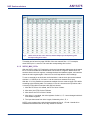
AN11275
SGPIO on the LPC4300
Rev. 1.1 — 13 November 2012
Application note
Document information
Info
Content
Keywords
SGPIO, LPC4300, PWM
Abstract
A guide how to set up and use SGPIO on the LPC4300 series
AN11275
NXP Semiconductors
SGPIO on the LPC4300
Revision history
Rev
Date
Description
1.1
20121113
Added software.
1
20121107
Initial revision.
Contact information
For more information, please visit: http://www.nxp.com
For sales office addresses, please send an email to: [email protected]
AN11275
Application note
All information provided in this document is subject to legal disclaimers.
Rev. 1.1 — 13 November 2012
© NXP B.V. 2012. All rights reserved.
2 of 20
AN11275
NXP Semiconductors
SGPIO on the LPC4300
1. Introduction
This application note explains the basics of SGPIO, how to work with it and what is
possible. It also includes a simple example that emulates PWM via SGPIO, designed for
engineers that haven't worked with SGPIO and need something to get started. The
example generates one PWM signal per SGPIO slice, giving a maximum of 16 extra
PWM channels. These channels are 5-bit PWM channels that can be fully on or off with
an adjustable frequency. The code is tested on the Keil MCB4300 with Keil 4.53.
AN11275
Application note
All information provided in this document is subject to legal disclaimers.
Rev. 1.1 — 13 November 2012
© NXP B.V. 2012. All rights reserved.
3 of 20
AN11275
NXP Semiconductors
SGPIO on the LPC4300
2. What is SGPIO?
Serial GPIO is a new digital configurable peripheral available on the LPC43XX devices
from NXP.
With SGPIO it is possible to create serial data protocols with very little CPU load
compared to bit banging.
SGPIO’s basic building block is slice. The slice is the hardware part that handles the data
processing when sending or receiving data. There are a total of 16 SGPIO slices and 16
SGPIO IO pins in the SGPIO interface.
Fig 1 shows the basic components inside a slice. A slice basically consists of a 32-bit
FIFO (main register REG in Fig 1) that is used to clock data in or out, a shadow register
(REG_SS register in Fig 1) for setting up the output data or receiving the input data, a
12-bit down counter to generate the shift clock and an 8-bit down counter to control the
number of bits shifted in or out.
Fig 1.
Block diagram of a single slice
The slice’s shift clock can be sourced from the SGPIO peripheral clock
(SGPIO_CLOCK). Please refer to Fig 2 below to understand SGPIO_CLOCK’s base
clock, and section 5.1 for more SGPIO_CLOCK setup.
AN11275
Application note
All information provided in this document is subject to legal disclaimers.
Rev. 1.1 — 13 November 2012
© NXP B.V. 2012. All rights reserved.
4 of 20
AN11275
NXP Semiconductors
SGPIO on the LPC4300
Fig 2.
Table 209 of the user manual, SGPIO clocking and power control
At every SGPIO_CLOCK, the 12-bit down counter (COUNT in Fig 1) counts down by 1.
When this 12-bit down counter (COUNT) reaches zero, a data bit is shifted in or out of
the FIFO (main register REG). Then COUNT is reloaded with the value in the PRESET
register. Therefore, the value in the PRESET register determines the shift clock speed.
Frequency (shift clock) = Frequency (SGPIO_CLOCK) / (PRESET+1)
Each slice includes an 8-bit down counter (register POS in Fig 1) that controls the
number of bits shifted in or out of the slice. Every time the COUNT register reaches zero
a data bit is shifted in or out of the FIFO and the POS register decrements by 1. When
the POS register reaches zero it is reloaded with the value in POS_PRESET and the
main register REG and its shadow register (REG_SS)’s contents get exchanged. For an
output slice new data is written to the shadow register and when the slice is done
sending the data in the main buffer the two buffers get exchanged. For an input slice new
data is clocked in the main buffer and when the slice is done collecting the data in the
main buffer the two buffers get exchanged.
Hence, to exchange the main register and the shadow register every m bit the
POS_PRESET should be set up as m-1. To exchange the content every k*32 bit
POS_PRESET should be 0x20 * k – 1. This setting should be used when k slices are
concatenated.
Tip 1: The POS register is divided into two parts, the POS counter and the POS
counter’s preset value. Please refer to Table 222 in the user manual for details.
Fig 3.
Table 222 of the user manual, Position register
Tip 2: An SGPIO pin is not the same as an SGPIO slice; a pin number is not equal to a
slice number! A slice connects to an SGPIO pin using a pin mux. Because of this one
slice can be connected to multiple pins and multiple slices can be concatenated to one
SGPIO pin. An SGPIO slice can be connected to 1, 2, 4 or 8 SGPIO pins. Up to eight
slices can be concatenated to input or output through one SGPIO pin.
AN11275
Application note
All information provided in this document is subject to legal disclaimers.
Rev. 1.1 — 13 November 2012
© NXP B.V. 2012. All rights reserved.
5 of 20
AN11275
NXP Semiconductors
SGPIO on the LPC4300
Tip 3: The slices are identified by letter A to letter P. Slice A is the first slice, slice B is the
second slice and so on.
3. SGPIO usage
SGPIO can be used to "emulate" serial protocols in those cases when an additional
SPI/I2C/UART is needed.
SGPIO can also be used to create fast serial and parallel protocols like PWM, e.g.,
reading in parallel data from a camera module and display/VGA generation.
The max speed of a clock signal that can be generated with SGPIO is half the clock
speed of the CPU. Therefore, the absolute max speed of the SGPIO_CLOCK is 102 MHz
when using the maximum 204 MHz CPU clock.
A complex example for a 7.1 soundcard can be downloaded from
http://lpcware.com/content/project/lpc4350-hitex-board-getting-started-guide
It connects to a computer via USB and uses SGPIO to send audio data from USB to four
stereo I2S DACs.
A simple example that creates a PWM signal is provided with this document.
4. Register descriptions
SGPIO is an extremely flexible peripheral. With that flexibility a lot of options are
possible, but it also means there are a lot of registers to set up. The registers are divided
in four groups:
1. Registers for slice/SGPIO pin multiplexing control
2. Registers for slice operation control (double buffering and shift clock control)
3. Registers for interrupt specific settings
4. Registers for SGPIO pin control
Note: The following information is meant to accompany and expand on chapter 18.6 of
the user manual, which provides an explanation of all available register settings in the
SGPIO.
4.1 Slice/SGPIO pin multiplexing registers
For this group of registers, replace ‘x’ with the correct number for the slice. 0 for slice A, 1
for slice B, 2 for slice C and so on.
4.1.1 OUT_MUX_CFGx
The OUT_MUX_CFG register is used to set up the output mode of the slice and how
many I/O pins are used in an output slice. It is possible for one SGPIO slice to use 1, 2, 4
or 8 I/O pins. Bits 3:0 control how many pins are used in the different slice output
configurations or whether the corresponding pin is for shift clock output or GPIO output.
AN11275
Application note
All information provided in this document is subject to legal disclaimers.
Rev. 1.1 — 13 November 2012
© NXP B.V. 2012. All rights reserved.
6 of 20
AN11275
NXP Semiconductors
SGPIO on the LPC4300
Fig 4.
Table 212 of the user manual, Output pin multiplexer configuration
register OUT_MUX_CFG
Bits 6:4 determine how the output enable is controlled. The output enable can be
controlled by the GPIO_OENREG register or by a different slice according to the
configuration above. The output states include low or high in active mode or tri-state
when disabled.
In the following table the output pin multiplexing can be found.
AN11275
Application note
All information provided in this document is subject to legal disclaimers.
Rev. 1.1 — 13 November 2012
© NXP B.V. 2012. All rights reserved.
7 of 20
AN11275
NXP Semiconductors
SGPIO on the LPC4300
Fig 5.
Table 213 from the user manual, SGPIO Output pin multiplexing and
corresponding slice letter
This table can be found on page 353/354 of the user manual Rev 1.3. For example,
when SGPIO pin 1 is used in 1-bit mode the corresponding slice is slice I.
4.1.2 SGPIO_MUX_CFGx
With the SGPIO_MUX_CFG register the clock and concatenate settings can be changed.
Bit 11 is used to enable slice concatenation. When this bit is high the SGPIO slice will
send the data in the main register, exchange the data and shadow register, and send the
data in the main register again. If this bit is low it will stop after the first exchange.
To use an external pin as shift clock bit 0 should be 1 and the clock pin can be selected
with bits 2:1; SGPIO pin 8, 9 10 and 11 can be used as an external clock input.
With bits 13:12 it is possible to concatenate multiple slices to create a bigger FIFO buffer
according to the following table. For example, if slice A is chosen as an input slice and a
4 slice big FIFO buffer is used the buffer will look like this:
1. After the FIFO from A is shifted, the FIFO of slice I follows.
2. After slice I the FIFO of slice E follows.
3. After slice E the FIFO of slice J follows.
4. After slice J is complete, the main registers of slice A, I, E, J are exchanged with their
own shadow registers.
5. The input then starts from slice A again, followed by slice I, E, J.
NOTE: In the programming code the data registers of slice A, I, E and J should all be
handled and should be seen as one big 128-bit FIFO buffer.
AN11275
Application note
All information provided in this document is subject to legal disclaimers.
Rev. 1.1 — 13 November 2012
© NXP B.V. 2012. All rights reserved.
8 of 20
AN11275
NXP Semiconductors
SGPIO on the LPC4300
Fig 6.
Fig 38. from the user manual, Concatenation Interconnections
4.1.3 SLICE_MUX_CFGx
With the SLICE_MUX_CFG register, a couple of settings can be used. When using the
data match interrupt bit 0 has to be high. When using data match mode, the slice’s
shadow register should hold the pattern to be matched. In addition, when data match is
enabled the main register and the shadow register will not exchange when FIFO is done
with input or output data. With bit 2 the clock input can be chosen; 0 for the internal clock
and 1 to use an external clock. It works only when this bit and SGPIO_MUX_CFG are set
to use an external clock.
With bits 5:4 the input bit match interrupt mode can be selected: 0b00 for rising edge,
AN11275
Application note
All information provided in this document is subject to legal disclaimers.
Rev. 1.1 — 13 November 2012
© NXP B.V. 2012. All rights reserved.
9 of 20
AN11275
NXP Semiconductors
SGPIO on the LPC4300
0b01 for falling edge, 0b10 for low level, 0b11 for high level. With bits 6:7 the amount of
bits that are shifted out per clock can be chosen. When a slice has multiple I/O pins this
value has to be set accordingly: 0b00 for 1 bit, 0b01 for 2 bits, 0b10 for 4 bits or 0b11 for
8 bits per clock.
4.2 Slice operation control registers
4.2.1 REGx
This is the data register. As long as a slice is enabled it will shift a data bit in or out at
every shift clock. Data is right shifted, data is shifted in at bit 31 and data is shifted out
from bit 0.
4.2.2 REG_SSx
This is the shadow register for the data. Every time a slice is done with sending or
receiving data it exchanges the data and shadow register. This way the shadow register
can be read or written at any time.
4.2.3 PRESETx
With the PRESETx register the SGPIO_CLOCK can be divided down to a lower speed.
To calculate the value for this register the following formula is used:
PRESETx value = (SGPIO_CLOCK speed / shift clock speed) – 1. When a 1.5 MHz
clock speed is required for a slice and a 12 MHz SGPIO clock is used the correct
PRESETx value is (12/1.5) – 1 = 7.
4.2.4 POSx
Each position register contains the position counter for one slice: POS0 to POS15
contain the counter for slice A (register 0) to slice P (register 15).
This register controls when the shadow register REG_SS content is exchanged with
main register REG.
It has [15:8] as the POS_PRESET value and [7:0] as the current data bit POS counter. At
each data bit shift, POS decrements by 1. When POS reaches zero, POS is restored with
its POS_PRESET value. This should be 31 when the main register and the shadow
register exchange after all 32 bits of data have shifted in or out.
But when concatenating k slices this value should be (0x20 * k -1). For example, when
concatenating 4 slices and every slice needs to shift in or out all of its 32-bit data, POSx
should be (32 * 4 - 1) = 127. Please refer to Fig 3 for some more details for this register.
Tip 4. Before a slice is started (using CTRL_ENABLE), POS should be set to the
POS_PRESET value.
4.2.5 MASK_A, MASK_H, MASK_I, MASK_P
The mask registers are used for the “on pattern match” interrupts. With some slices it is
possible to mask the data for the pattern match interrupts. Slices A, H, I and P support
this function.
Every bit that is 1 in this register will be masked. If this register contains the value
0b00001111 the first 4 bits will be masked for the pattern interrupt.
See chapter 6, SGPIO Interrupts for more information.
AN11275
Application note
All information provided in this document is subject to legal disclaimers.
Rev. 1.1 — 13 November 2012
© NXP B.V. 2012. All rights reserved.
10 of 20
AN11275
NXP Semiconductors
SGPIO on the LPC4300
4.2.6 CTRL_ENABLE
With the CTRL_ENABLE register set to 1 for a particular bit the corresponding slice’s 12bit COUNT down counter or external shift clock is started to provide the data shift clock
for the slice.
4.2.7 CTRL_DISABLE
With the CTRL_DISABLE register set to 1 for a particular bit the corresponding slice’s
COUNT clocks or external shift clock is disabled. When this register is set, it
synchronously disables the POSx counter when POSx counter reaches a zero count.
The CTRL_DISABLED register is not cleared at that time: it remains set.
Tip 5. When starting COUNTx (by setting CTRL_ENABLE), this register should be set
after COUNTx is started with register CTRL_ENABLE.
4.3 SGPIO interrupt specific registers
For these interrupt specific registers, replace the x with the correct number for the
interrupt. 0 for shift clock; 1 for main register and shadow register exchange; 2 for data
pattern match and 3 for input bit match.
4.3.1 CLR_EN_x
This register is used to disable interrupts. Slice interrupts can be disabled by writing a 1
to the register. For example, if a 1 is written to bit 2 the interrupt for slice C will be
disabled.
4.3.2 SET_EN_x
This register is used to enable interrupts. Slice interrupts can be enabled by writing a 1 to
the register. If, for example, a 1 is written to bit 3 the interrupt for slice D will be enabled.
4.3.3 ENABLE_x
Reading out this register will return what slices have their interrupts enabled. If this
register contains the value 0b1001 that means slice A and D have the interrupts enabled.
4.3.4 STATUS_x
Reading out this register will return on which slices an interrupt has happened. It is
possible that an interrupt happens on multiple slices at the same time. If this register
contains the value 0b1000100 interrupts happened on slice C and G.
4.3.5 CTR_STAT_x
This register is used to clear the interrupt state. It is recommended to clear all interrupt
states after handling the interrupts otherwise the value in the STATUS_x register will also
contain old interrupt states.
4.3.6 SET_STAT_x
This register is used to set interrupt states. When a 1 is written to bit 0 it will look like an
interrupt happened on slice A. This register can be used for code testing.
4.4 SGPIO pin control registers
These registers are used to control SGPIO pin status. GPIO_INREG, GPIO_OUTREG
and GPIO_OENREG are SGPIO pin based. This means that they control SGPIO pins
and not slices. If a 1 is written to bit 2 this will effect SGPIO pin 2 and not slice C.
AN11275
Application note
All information provided in this document is subject to legal disclaimers.
Rev. 1.1 — 13 November 2012
© NXP B.V. 2012. All rights reserved.
11 of 20
AN11275
NXP Semiconductors
SGPIO on the LPC4300
4.4.1 GPIO_INREG
With this register the SGPIO pins can be made an input. When a 1 is written to bit 2
SGPIO pin 2 will be an input. Note: The SGPIO pin must be made an input with the
pinmux too. See chapter 15 of the user manual from the LPC4300 for more information
about the pinmux. NOTE: Concatenate cannot be set to self loop when using an SGPIO
pin as input.
4.4.2 GPIO_OUTREG
With this register the SGPIO pins can be made an output. When a 1 is written to bit 3
SGPIO pin 3 will be an output.
4.4.3 GPIO_OENREG
With the GPIO_OENREG register an SGPIO output pin can be enabled. An SGPIO pin
must be enabled in order to work. When a 1 is written to bit 3 SGPIO pin 3 will be
enabled. To disable an SGPIO pin a 0 has to be written to the corresponding bit.
5. Steps to get SGPIO working
To get SGPIO up and running:
1. Select the right clock
2. Set up the registers, slices used, IO pins used, concatenate slices, etc.
3. Set up the interrupts
4. Handle interrupts and data
5.1 Selecting the right clock signal
First the clock speed has to be selected. By default SGPIO uses the IRC, which runs at
12 MHz. Other clock sources can be selected too; by selecting PLL1 SGPIO can run on
the same clock speed as the LPC4300. In the PWM example the following line of code
can be found in lpc43xx_cgu.c:
IRC:
LPC_CGU->BASE_PERIPH_CLK = (0x1 << 24);
PLL1:
LPC_CGU->BASE_PERIPH_CLK = (0x9 << 24);
For more information, see page 105 of the LPC4300 user manual.
5.2 Set up the registers
After knowing how many SGPIO pins are going to be used, and how they will be used,
the registers can be set up. The registers that need to be set up are OUT_MUX_CFGx,
SGPIO_MUX_CFGx, SLICE_MUX_CFGx, PRESETx, COUNTx, POSx, REGx and
REG_SSx. The first three registers control most of the slice settings such as: number of
slices concatenated, number of SGPIO pins per slice, input or output, what clock is used
etc.
Depending on the interrupts used to handle the data the interrupt registers must be set
up too. Also in the pinmux the IO pins must be set up as SGPIO pin and as input or
output. To start SGPIO the clock signals must be enabled. This is done by setting bits 15
and 12 in the CTRL_ENABLED register. An example how to set up the SGPIO registers
for I2S use can be found in the user manual on page 376 to 379.
AN11275
Application note
All information provided in this document is subject to legal disclaimers.
Rev. 1.1 — 13 November 2012
© NXP B.V. 2012. All rights reserved.
12 of 20
AN11275
NXP Semiconductors
SGPIO on the LPC4300
5.3 Set up interrupts
The interrupt description can be found in chapter 6 of this document.
5.4 Handling data
When everything is set up and SGPIO is running the data still needs to be handled. What
to do with the incoming and outgoing data is up to the user and depends on the
application. When emulating a bus protocol like UART, SPI or I2C the protocol itself has
to be made by software. Data arrives in 32-bit blocks. UART uses 10-bit blocks (start bit,
8-bit data, stop bit) and SPI and I2C use 8-bit blocks. This translation has to be made in
software and is different per bus protocol. When using SGPIO to communicate with a
camera module or some other parallel bus the same story applies.
Speeds over 40 MHz are doable and CPU load can be lowered by concatenating slices.
When using 4 or 8-bit wide busses it is recommended to concatenate 2, 4 or 8 slices for
a larger buffer. If the buffer is 32-bit and an 8-bit bus is used the buffer is full in just 4
SGPIO clock cycles. When 8 slices are concatenated a 256-bit buffer is created and it
takes 32 SGPIO clock cycles to fill this buffer, a much lower CPU load.
6. SGPIO Interrupts
There are four interrupt methods available for SGPIO, they are:
1. On shift clock
2. On data exchange clock
3. On data pattern match
4. On input bit match (rising/falling edge, high/low level)
6.1 On shift clock
When enabled through SET_EN, this interrupt occurs every time COUNTx equals 0. This
normally happens every time 1 data bit is clocked out or in of an SGPIO slice and can be
CPU intensive. The registers used for this interrupt are:
• CLR_EN_0
• SET_EN_0
• ENABLE_0
• STATUS_0
• CTR_STATUS_0
• SET_STATUS_0
6.2 On data exchange (swap) clock
When enabled through SET_EN, this interrupt will occur every time the data between the
Data register (REGx) and the shadow register (REG_SSx) is exchanged. This interrupt
can be used to place new data in the shadow register, at the next exchange (and
interrupt) the new data will be loaded in the data register and new data can be put in the
shadow register. The registers used for this interrupt are:
• CLR_EN_1
• SET_EN_1
• ENABLE_1
AN11275
Application note
All information provided in this document is subject to legal disclaimers.
Rev. 1.1 — 13 November 2012
© NXP B.V. 2012. All rights reserved.
13 of 20
AN11275
NXP Semiconductors
SGPIO on the LPC4300
• STATUS_1
• CTR_STATUS_1
• SET_STATUS_1
6.3 On data pattern match
It is possible to interrupt when a certain pattern is clocked in or out. Slices A, I, H and P
also support mask functionality for the pattern match interrupt. The pattern match
interrupt can be used to look for certain data when making a logic or data analyzer.
To use this interrupt, bit 0 from register SLICE_MUX_CFGx must be high. The pattern
can be up to 32-bit long and should program in REG_SS register. If the data in the data
register matches the data in the shadow register an interrupt will happen. As long as this
interrupt is enabled and bit 0 in SLICE_MUX_CFGx is high the data register and shadow
register will not swap.
The registers used for this interrupt are:
• CLR_EN_2
• SET_EN_2
• ENABLE_2
• STATUS_2
• CTR_STATUS_2
• SET_STATUS_2
6.4 On input bit match
When enabled through SET_EN, it is possible to interrupt on a low or high level or on a
falling or rising edge on the input data bit.
The registers used for this interrupt are:
• CLR_EN_3
• SET_EN_3
• ENABLE_3
• STATUS_3
• CTR_STATUS_3
• SET_STATUS_3
6.5 Using interrupts
Using the interrupts is more or less the same for all 4. Enabling/disabling the interrupts is
done with the SET_EN and CLR_EN register. If, for example, bit 7 is high then the
interrupt for Slice H is enabled/disabled. Reading out the interrupts is done via the
STATUS register. Setting/clearing interrupts is done by writing to the SET_STAT and
CTR_STAT register.
To handle an interrupt you have to find out what slice caused the interrupt, run the actual
code and clear the interrupt. For example, a piece of code to handle a data exchange
clock interrupts on slice P:
void SGPIO_IRQHandler (void)
AN11275
Application note
//Handles all SGPIO interrupts
All information provided in this document is subject to legal disclaimers.
Rev. 1.1 — 13 November 2012
© NXP B.V. 2012. All rights reserved.
14 of 20
AN11275
NXP Semiconductors
SGPIO on the LPC4300
{
uint32_t tempvar = 0;
//temp variable to store interrupts
tempvar = LPC_SGPIO->STATUS_1;
//Read data exchange
interrupt register
if(tempvar & 0x8000)
//If a capture clock interrupt on the
SGPIO slice 15 happened...
{
//code to send new data or handle data should be placed here
}
LPC_SGPIO->CTR_STATUS_1 = 0xFFFF; //Clear the interrupts
}
7. PWM example
An example is provided that uses SPGIO to create PWM signals, a flowchart of this
example can be found on the next page. Every SGPIO pin can be used as an extra PWM
pin in this way. The duty cycle and frequency can be changed on the fly. As one slice has
a 32-bit FIFO buffer there are only 33 PWM duty cycles possible, so essentially it's a 5-bit
PWM that can be fully on or fully off. When concatenating slices a bigger precision can
be reached but to make this example simple this is not implemented.
A slice is used as output and the PWM data is loaded in the REG and REG_SS data
registers. After that the slice only has to repeat the data in the REG register. When the
PWM duty cycle is changed the value in the REG_SS register will be updated twice. This
is because every 32 clock cycles the REG and REG_SS register is swapped. If the data
is only written in the REG_SS register once only half of the time the PWM output would
be correct and half of the time it would be the old value.
When the command is executed to edit a PWM value the interrupts are switched on.
When the next swap between REG and REG_SS occurs the new data is loaded into the
REG_SS register. When another data swap occurs this happens again. After this the
interrupts are switched off and the PWM duty cycle is changed. A flowchart of this can be
found on the next page.
As the example uses internal clock (COUNT) and enables with OENREG and each PWM
channel uses only one output slice, OUT_MUX_CFG, SLICE_MUX_CFG are 0. The data
in the REG register has to be repeated so SGPIO_MUX_CFG bit 11 is set high. This
means the slice is in self loop mode and will repeat the data in the REG register. The
clock speed is dependent of what the user wants so it is calculated and then stored in the
PRESET register. As we exchange the REG and REG_SS registers every 32 bit, the
POS_PRESET is 0x1F.
When the SGPIO slice is set up as a PWM pin the frequency can be specified by the
user. The code calculates the correct divider PRESET setting by the following formula.
PWM frequency * 32 = SGPIO_CLOCK / (PRESET +1)
Note the “* 32” in the above equation, this is because the PWM signal frequency is 32
times of the shift clock frequency.
AN11275
Application note
All information provided in this document is subject to legal disclaimers.
Rev. 1.1 — 13 November 2012
© NXP B.V. 2012. All rights reserved.
15 of 20
AN11275
NXP Semiconductors
SGPIO on the LPC4300
Fig 7.
AN11275
Application note
Flowchart of the code when changing a PWM value
All information provided in this document is subject to legal disclaimers.
Rev. 1.1 — 13 November 2012
© NXP B.V. 2012. All rights reserved.
16 of 20
AN11275
NXP Semiconductors
SGPIO on the LPC4300
7.1 How to use the SGPIO PWM library
The SGPIO PWM library has four commands:
•
void SGPIOPWMinit(void);
•
void SGPIOPWMchaninit(uint32_t freq, uint8_t channel);
•
void SGPIOPWMValue(uint8_t value, uint8_t channel);
•
uint8_t SGPIOPWMstatus();
SGPIOPWMinit initializes SGPIO for PWM use. It disables all interrupts, makes all
SGPIO slices an output and enables all SGPIO clocks. This command should be
executed before the other commands are used.
SGPIOPWMchaninit is the command to initialize an SGPIO slice for PWM use. It can
also be used to change the PWM frequency at any moment but can cause a small hiccup
in the PWM signal. “freq” is the desired PWM frequency in hertz. The maximum
frequency is the core clock divided by 64 (because the shift clock frequency is 32 times
of the PWM frequency). As it uses a divider the actual speed will be an approximate of
the given frequency. “channel” is the SGPIO slice that should be adjusted. This
command has to be executed before the SGPIOPWMValue works.
SGPIOPWMValue is used to change the PWM duty cycle of any slice. As it is a 5-bit
PWM that can be fully on or off there are 33 values. 0 is a 0% duty cycle, 33 is a 100%
duty cycle and 16 is ~47% duty cycle. Channel is the SGPIO slice that should be
adjusted.
After adjusting the duty cycle of a slice the command SGPIOPWMstatus can be used to
check if the adjusting is done so another slice can be adjusted. If it returns 0 adjusting is
done and the SGPIOPWMValue can be used again.
Before an IO pin can be used as SGPIO pin the correct setup has to be loaded in the
pinmux. The settings possible per IO pin can be found in chapter 14, LPC43xx Pin
configuration in the user manual. For example, to use P0_0 as SGPIO pin function 3
(SGPIO0) has to be selected. The correct command for this is:
scu_pinmux(0x0, 0 , MD_PLN, FUNC3);
The example code uses P1.1, P2.6 and P2.8 to show some effects on a RGB LED. To
see this effect a common anode RGB LED should be connected to P1.1, P2.6 and P2.8.
AN11275
Application note
All information provided in this document is subject to legal disclaimers.
Rev. 1.1 — 13 November 2012
© NXP B.V. 2012. All rights reserved.
17 of 20
AN11275
NXP Semiconductors
SGPIO on the LPC4300
8. Conclusion
SGPIO is a very flexible peripheral that can be used to emulate a lot of serial and parallel
busses, but can also be used to generate signals or to read in signals. NXP provides
examples for emulating I2C, SPI and generating PWM signals. With these examples it
will be easier to get started with SGPIO and use it for a custom application or to solve a
shortage of peripherals. Because it is possible to emulate peripherals on a lot of IO ports
this can make PCB design easier and make the LPC43xx more flexible for power creeps
where in other cases a new microcontroller would have been necessary. Combined with
other new peripherals like the State Configurable Timer, SPIFI Flash and the M0
coprocessor it makes the LPC43xx a flexible and powerful microcontroller that is easy to
work with.
AN11275
Application note
All information provided in this document is subject to legal disclaimers.
Rev. 1.1 — 13 November 2012
© NXP B.V. 2012. All rights reserved.
18 of 20
AN11275
NXP Semiconductors
SGPIO on the LPC4300
9. Legal information
9.1 Definitions
Draft — The document is a draft version only. The content is still under
internal review and subject to formal approval, which may result in
modifications or additions. NXP Semiconductors does not give any
representations or warranties as to the accuracy or completeness of
information included herein and shall have no liability for the consequences
of use of such information.
9.2 Disclaimers
Limited warranty and liability — Information in this document is believed to
be accurate and reliable. However, NXP Semiconductors does not give any
representations or warranties, expressed or implied, as to the accuracy or
completeness of such information and shall have no liability for the
consequences of use of such information. NXP Semiconductors takes no
responsibility for the content in this document if provided by an information
source outside of NXP Semiconductors.
In no event shall NXP Semiconductors be liable for any indirect, incidental,
punitive, special or consequential damages (including - without limitation lost profits, lost savings, business interruption, costs related to the removal
or replacement of any products or rework charges) whether or not such
damages are based on tort (including negligence), warranty, breach of
contract or any other legal theory.
Notwithstanding any damages that customer might incur for any reason
whatsoever, NXP Semiconductors’ aggregate and cumulative liability
towards customer for the products described herein shall be limited in
accordance with the Terms and conditions of commercial sale of NXP
Semiconductors.
Right to make changes — NXP Semiconductors reserves the right to make
changes to information published in this document, including without
limitation specifications and product descriptions, at any time and without
notice. This document supersedes and replaces all information supplied prior
to the publication hereof.
Suitability for use — NXP Semiconductors products are not designed,
authorized or warranted to be suitable for use in life support, life-critical or
safety-critical systems or equipment, nor in applications where failure or
malfunction of an NXP Semiconductors product can reasonably be expected
to result in personal injury, death or severe property or environmental
damage. NXP Semiconductors and its suppliers accept no liability for
inclusion and/or use of NXP Semiconductors products in such equipment or
applications and therefore such inclusion and/or use is at the customer’s
own risk.
Applications — Applications that are described herein for any of these
products are for illustrative purposes only. NXP Semiconductors makes no
representation or warranty that such applications will be suitable for the
specified use without further testing or modification.
Semiconductors accepts no liability for any assistance with applications or
customer product design. It is customer’s sole responsibility to determine
whether the NXP Semiconductors product is suitable and fit for the
customer’s applications and products planned, as well as for the planned
application and use of customer’s third party customer(s). Customers should
provide appropriate design and operating safeguards to minimize the risks
associated with their applications and products.
NXP Semiconductors does not accept any liability related to any default,
damage, costs or problem which is based on any weakness or default in the
customer’s applications or products, or the application or use by customer’s
third party customer(s). Customer is responsible for doing all necessary
testing for the customer’s applications and products using NXP
Semiconductors products in order to avoid a default of the applications and
the products or of the application or use by customer’s third party
customer(s). NXP does not accept any liability in this respect.
Export control — This document as well as the item(s) described herein
may be subject to export control regulations. Export might require a prior
authorization from competent authorities.
Evaluation products — This product is provided on an “as is” and “with all
faults” basis for evaluation purposes only. NXP Semiconductors, its affiliates
and their suppliers expressly disclaim all warranties, whether express,
implied or statutory, including but not limited to the implied warranties of noninfringement, merchantability and fitness for a particular purpose. The entire
risk as to the quality, or arising out of the use or performance, of this product
remains with customer.
In no event shall NXP Semiconductors, its affiliates or their suppliers be
liable to customer for any special, indirect, consequential, punitive or
incidental damages (including without limitation damages for loss of
business, business interruption, loss of use, loss of data or information, and
the like) arising out the use of or inability to use the product, whether or not
based on tort (including negligence), strict liability, breach of contract, breach
of warranty or any other theory, even if advised of the possibility of such
damages.
Notwithstanding any damages that customer might incur for any reason
whatsoever (including without limitation, all damages referenced above and
all direct or general damages), the entire liability of NXP Semiconductors, its
affiliates and their suppliers and customer’s exclusive remedy for all of the
foregoing shall be limited to actual damages incurred by customer based on
reasonable reliance up to the greater of the amount actually paid by
customer for the product or five dollars (US$5.00). The foregoing limitations,
exclusions and disclaimers shall apply to the maximum extent permitted by
applicable law, even if any remedy fails of its essential purpose.
9.3 Trademarks
Notice: All referenced brands, product names, service names and
trademarks are property of their respective owners.
Customers are responsible for the design and operation of their applications
and products using NXP Semiconductors products, and NXP
AN11275
Application note
All information provided in this document is subject to legal disclaimers.
Rev. 1.1 — 13 November 2012
© NXP B.V. 2012. All rights reserved.
19 of 20
AN11275
NXP Semiconductors
SGPIO on the LPC4300
10. Contents
1.
2.
3.
4.
4.1
4.1.1
4.1.2
4.1.3
4.2
4.2.1
4.2.2
4.2.3
4.2.4
4.2.5
4.2.6
4.2.7
4.3
4.3.1
4.3.2
4.3.3
4.3.4
4.3.5
4.3.6
4.4
4.4.1
4.4.2
4.4.3
5.
5.1
5.2
5.3
5.4
6.
6.1
6.2
6.3
6.4
6.5
7.
7.1
8.
9.
9.1
9.2
Introduction ......................................................... 3
What is SGPIO? ................................................... 4
SGPIO usage........................................................ 6
Register descriptions .......................................... 6
Slice/SGPIO pin multiplexing registers............... 6
OUT_MUX_CFGx .............................................. 6
SGPIO_MUX_CFGx .......................................... 8
SLICE_MUX_CFGx ........................................... 9
Slice operation control registers ....................... 10
REGx ............................................................... 10
REG_SSx ......................................................... 10
PRESETx ......................................................... 10
POSx ................................................................ 10
MASK_A, MASK_H, MASK_I, MASK_P .......... 10
CTRL_ENABLE................................................ 11
CTRL_DISABLE............................................... 11
SGPIO interrupt specific registers .................... 11
CLR_EN_x ....................................................... 11
SET_EN_x ....................................................... 11
ENABLE_x ....................................................... 11
STATUS_x ....................................................... 11
CTR_STAT_x ................................................... 11
SET_STAT_x ................................................... 11
SGPIO pin control registers.............................. 11
GPIO_INREG ................................................... 12
GPIO_OUTREG ............................................... 12
GPIO_OENREG ............................................... 12
Steps to get SGPIO working ............................. 12
Selecting the right clock signal ......................... 12
Set up the registers .......................................... 12
Set up interrupts ............................................... 13
Handling data ................................................... 13
SGPIO Interrupts ............................................... 13
On shift clock.................................................... 13
On data exchange (swap) clock ....................... 13
On data pattern match ..................................... 14
On input bit match ............................................ 14
Using interrupts ................................................ 14
PWM example .................................................... 15
How to use the SGPIO PWM library ................ 17
Conclusion ......................................................... 18
Legal information .............................................. 19
Definitions ........................................................ 19
Disclaimers....................................................... 19
9.3
10.
Trademarks ......................................................19
Contents .............................................................20
Please be aware that important notices concerning this document and the product(s)
described herein, have been included in the section 'Legal information'.
© NXP B.V. 2012.
All rights reserved.
For more information, visit: http://www.nxp.com
For sales office addresses, please send an email to: [email protected]
Date of release: 13 November 2012
Document identifier: AN11275