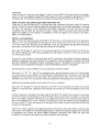
1
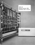
DRV11-P FOUNDATION
MODULE USER'S
MANUAL
EK-DRVII-0P-002
DRV11-P FOUNDATION
MODU LE USER'S
MANUAL
digital equipment corporation • marlborough, massachusetts
1st Edition September 1976
2nd Edition (rev) March 1977
Copyright © 1976, 1977 by Digital Equipment Corporation
The material in this manual is for informational
purposes and is subject to change without notice.
Digital Equipment Co.-poration assumes no responsibility for any errors which may appear in this
manual.
Printed in U.S.A.
The following are trademarks of Digital Equipment
Corporation, Maynard, Massachusetts:
DEC
DECCOMM
DECsystem.l0
DECSYSTEM·20
DECtape
DEC US
DIGITAL
MASSBUS
PDP
RSTS
TYPESET·S
TYPESET·l!
UNIBUS
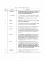
CONTENTS
Page
INTRODUCTION . . . . . . . . . . . . . . . . . . . . . . . . . . . . . . . . . . . . . . . . . . . . . .
SPECIFICATIONS . . . . . . . . . . . . . . . . . . . . . . . . . . . . . . . . . . . . . . . . . _. . . .
Physical . . . . . . . . . . . . . . . . . . . . . . . . . . . . . . . . . . . . . . . . . . . .
Dimensions . . . . . . . . . . . . . . . . . . . . . . . . . . . . . . . . . . . . . . . . . .
User IC Capacity . . . . . . . . . . . . . . . . . . . . . . . . . . . . . . . . . . . . . . .
Weight . . . . . . . . . . . . . . . . . . . . . . . . . . . . . . . . . . . . . . . . . . . .
Electrical . . . . . . . . . . . . . . . . . . . . . . . . . . . . . . . . . . . . . . . . . . .
Environmental Temperature . . . . . . . . . . . . . . . . . . . . . . . . . . . . . . . .
Relative Humidity . . . . . . . . . . . . . . . . . . . . . . . . . . . . . . . . . . . . . .
FUNCTIONAL DESCRIPTION . . . . . . . . . . . . . . . . . . . . . . . . . . . . . . . . . . . . . .
Bus Transceivers . . . . . . . . . . . . . . . . . . . . . . . . . . . . . . . . . . . . . . .
Device Address Comparator . . . . . . . . . . . . . . . . . . . . . . . . . . . . . . .
Device Address Selection . . . . . . . . . . . . . . . . . . . . . . . . . . . . . . . . . .
Protocol Logic . . . . . . . . . . . . . . . . , . . . . . . . . , . , . . . , . . . . . . . .
Interrupt Logic . . . . . . . . . . . . . . . . . . . . . . . . . . . . , . . . . . . . . . . .
Vector Address Generator . . . . . . . . . . . . . . . . . . . . . . . . . . . . . . . . .
Vector Address Selection
Bus Receivers . . . . . . . . . . . . . . . . . . . . . . . . . . . . . . . . . . . . . . . .
+3V Source . . . , . . . . . . . . . . . . . . . . . . . . . . . . . . . . . . , . . . . . , .
USER I/O LINES AND ASSOCIATED WIRE-WRAP PINS (WP) . . . . . . . . . , . . . , . . . . .
PHYSICAL DESCRIPTION . . . , , . . . . . , .. , . . . . . . . . . . . . . . , . . . . . , , , , . ,
MODULE INSTALLATION . . . . . . . . . . . . . . . . . , . . . . . . . . . . . . . . . . , . . . . .
WIRE-WRAP TOOLS ., . . . . . . . . . . . . . . . . . . . . . . . . . . . . . . . . . . . . . . , ..
DRVII-P PARTS LIST . . . . . . , .. , . . . . . . . . . . . . . . . . . . . , . . . . . . , . . . .
RELATED LITERATURE . . . . . . . . . . . . . . . . . , . . . . . . . . . . . . . . . . . . . . . .
1
1
1
1
2
2
2
2
2
2
2
5
5
6
6
7
17
17
18
18
18
21
21
21
21
APPENDIX A - IC DESCRIPTIONS . . . . . . . . . . . . . . . . . . . . . . . . . . . . . , . . ..
A.I
DC003 INTERRUPT LOGIC . . . . . . . . . . . . . . . . . . . . . . . . . . . ..
A.2
DC004 PROTOCOL LOGIC. . . . . . . . . . . . . . . . . . . . . . . . . . . . ..
A-I
A-I
A-I
ILLUSTRAnONS
Figure No.
1
2
3
4
5
A-I
A-2
A-3
Title
D RV Il-P Basic Block Diagram . . . . . . . . . . . . . . . . . . . . . . . . . . . . . . .
DRVll-P Block Diagram (Bus Transceivers, Device Address Comparator,
and Protocol Logic) . . . . . . . . . . . . . . . . . . . . . . . . . . . . . . . . . . . . .
DRVII-P Device Address Select Format . . . . . . . . . . . . . . . . . . . . . . . . .
DRVI1-P Vector Address Select Format . . . . . . . . . . . . . . . . , . . . . . . ..
DRVI1-P Physical Layout . . . . . . . . . . . . . . . . . . . . . . . . . . . . . . . ..
DC003 Simplified Logic Diagram . . . . . . . . . . . . . . . . . . . . . . . . . . . . .
DC003 "A" Interrupt Section Timing Diagram. . . . . . . . . . . . . . . . . . . . ..
DC003 "A" and "B" Interrupt Sections Timing Diagrams . . . . , . . . . . . . . ..
iii
Page
3
5
17
19
A-2
A-3
A-4
ILLUSTRATIONS (Cont)
Figure No.
A-4
A-5
A-6
Title
Page
DC004 Simplified Logic Diagram . . . . . . . . . . . . . . . . . . . . . . . . . . . . . A-7
DC004 Timing Diagram . . . . . . . . . . . . . . . . . . . . . . . . . . . . . . . . . . . A-IO
DC004 Loading Configurations for Table A-2 . . . . . . . . . . . . . . . . . . . . . . A-II
TABLES
Table No.
I
2
3
4
5
6
A-I
A-2
A-3
Title
Page
C37R-C Delays for BRPLY . . . . . . . . . . . . . . . . . . . . . . . . . . . . . . . . .
6
User Wire-Wrap Pins . . . . . . . . . . . . . . . . . . . . . . . . . . . . . . . . . . . . .
8
Maximum DRVII-P IC Density (All Areas) . . . . . . . . . . . . . . . . . . . . . . . .
20
Recommended Cable Assemblies . . . . . . . . . . . . . . . . . . . . . . . . . . . . . .
20
Wire-Wrap Tools . . . . . . . . . . . . . . . . . . . . . . . . . . . . . . . . . . . . . . .
21
DRVII-P Parts List . . . . . . . . . . . . . . . . . . . . . . . . . . . . . . . . . . . . .
22
DC003 Pin/Signal Descriptions . . . . . . . . . . . . . . . . . . . . . . . . . . . . . . . A-5
DC004 Signal Timing vs Output Loading . . . . . . . . . . . . . . . . . . . . . . . . . A-8
DC004 Pin/Signal Descriptions . . . . . . . . . • . . . . . . . . . . . . . . . . . . . . A-12
iv
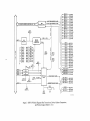
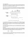
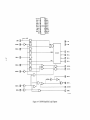
INTRODUCTION
The DRVII-P is an LSI-II bus compatible foundation wire-wrap interface module. Approximately
one-quarter of the module is occupied by bus transceivers, vector address generator logic, device
address comparator logic, protocol logic, and interrupt logic, as well as a 40-pin I/O connector. The
remaining three-quarters of the module are for user application and has plated-through holes to accept
IC's, and wire-wrap pins (WP) for interconnecting the user's circuits. The plated-through holes can
accept 6, 8, 14, 16, 18, 20, 22, 24, and 40-pin dual-in-line IC's or IC sockets in various mounting areas
of the module, or discrete components can be inserted into the plated-through holes. DRVII-P is a
quad height, extended length, single width module which can be inserted into anyone of the available
interface option locations of any LSI-II or PDP-II/03 backplane. The module occupies four
backplane slots. A basic block diagram illustrating the DRVII-P LSI-II bus interface logic is shown in
Figure I.
~
""
/
/'
'..
~
...
../
16 BUS DATA / ADDRESS LINES
1
BUS
RANSCEIVERS
VECTOR ENABLE
<I)
MUX
DEVICE
ADDRESS
COMPARATOR
:::>
CD
--
I
16 DATA INPUT LINES
'\..
.....
16 DATA/ADDR. OUTPUT LINES
VECTOR
ADDRESS
GENERATOR
B VECTOR ADDRESS LINES
A
/'
"-
P
V2- V7
"'I
::J
A
~
<-
SPARE 0-8
..
USER
ASSIGNED
VECTOR
ADDRESS
OPTIONAL
8-BIT
INPUT
BITS 03-12
TO /
FROM
USER'S
LOGIC
'I
I
H
,,11
<I)
...J
ENABLE
V'
~
BUS CONTROL SIGNALS
~
~
'\..
BITS 00-02
IN WD
PROTOCOL
LOGIC
OUT HB, OUT LB
SEL DEV 0 2 46
RQST A,B
ENB DATA A,B
~
"
BUS CONTROL SIGNALS
-)
v
INTERRUPT
LOGIC
VEC RQST
ENB A B ST
INIT
7'
11-4147
Figure I DRVII-P Basic Block Diagram
SPECIFICATIONS
The following specifications and particulars are for informational purposes only and are subject to
change without notice.
Physical
Quad-height, extended length, single-width module
Dimensions
10.5 in. H, 8.5 in. L, 0.5 in. W (26.67 em H, 21.59 em L, 1.27 em W)
User IC Capacity
Maximum IC density for all user areas is approximately 50 ICs, depending on IC types (see text for
particulars).
Weight
12 oz. (340 gr.)
Electrical
Bus Loading
DRVII-P presents a maximum of one LSI-II bus load to the bus.
User Lines
All user lines available at wire-wrap pins are TTL compatible; logic levels are as follows:
-
High = 1 = 2.0V min.
Low = 0 = 0.8V max.
Outputs -
High = 1 = 2.4V min.
Low = 0 = O.4V max.
Inputs
Bus Lines
All user bus lines available at wire-wrap pins have logic levels as follows:
Inputs Outputs -
High = 1 = 1.7V min.
Low = 0 = 1.3V max.
High = 1 = 2.0V min.
Low = 0 = 0.8V max.
Logic Power Requirements
+5V @ 1.0 A (max.) not including user logic.
Environmental
Temperature
Storage: - 40° to 66° C (- 40° to 150 0 F)
Operating: 5° to 50° C (41° to 122 0 F)
Relative Humidity
10% to 95% non-condensing
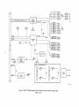
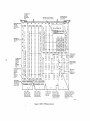
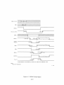
FUNCTIONAL DESCRIPTION
The DRVII-P is supplied with the logic necessary for interfacing to the LSI-II bus. This logic includes
bus transceivers, a device address comparator, protocol logicy interrupt logic, vector address
comparator, and bus receivers and inverters. Figure 2 shows the inter-relationship between the
aforementioned logic functions and the user's wire-wrap pins. A brief description of each logic
function is provided in the following paragraphs.
Bus Transceivers
Referring to Figure 2, sheet I, data output lines DOO through DIS reflect the state of the bus BDAL
lines and will contain address and data information for any bus transfer, regardless of the device
involved. Output data is usually clocked into a register for use by the interface or a peripheral since
the length of time that the data is available on the bus during the bus cycle is very short. The device
address comparator and the protocol logic determine if the data currently on the DOO-DIS lines is
intended for the DRVI1-P.
Input data present at the INOO-INI5 lines will be applied to the bus when the TRANS ENB A, B, C,
and D lines are asserted low. These lines are asserted by the protocol logic to gate data onto the bus at
2
INPUT DATA/ADDRESS LINES
16 BUS DATA/ADDRESS LINES (BDAL 0L -15L)
BUS
OUTPUT DATA/ADDRESS LINES
TRANSCEIVERS r-~~~~~~~~~~~--.
:I:
'"Ci
WP77
(BBS7 H)
I
:I:
o
o
o
D03H - D12H
BBS7 L
DEVICE
ADDRESS
COMPARATOR
BUS
RECEIVER
IN
IN
IN
IN
IN
IN
IN
IN
IN
IN
IN
IN
IN
IN
IN
IN
ENB H
:I:
'"0
0
WP31
(ENB H)
:::
:I:
0
0
I
WP10
(001 L)
:£
H
en
0
0
..J
0
BWTBT
BDOUT
BDIN
BSYNC
WP30
(002 L)
00
01
02
03
04
05
06
07
08
09
10
11
12
13
14
15
H
H
H
H
H
H
H
H
H
H
H
H
H
H
H
H
000
001
002
003
004
005
006
007
008
009
010
011
012
013
014
015
H
H
H
H
H
H
H
H
H
H
H
H
H
H
H
H
TRANS
TRANS
TRANS
TRANS
L
L
L
L
WPI13
(BSYNC H)
FROM
SHEET 2
VECTOR H
PROTOCOL
LOGIC
WORDIBYTE SELECT LINES
SPLIT
LUGS ~
WP20
(BRPLY L)
~_~ ~_J
WP12
(RXCX)
WP14
WP17
WP79
WP87
WP72
WPI17
WP107
WP88
WP106
WP61
WP91
WP109
WP85
WP84
WP83
WP81
B
A
C
0
L
L
L
L
WP100
WP120
WP94
WP95
DEVICE SELECT LINES
WP13
(BSYNC H)
BRPLY L
ENB
ENB
ENB
ENB
WP60
WP96
WP80
WP57
WP99
WP119
WP9B
WPI1B
WP113
WP92
WPB9
WP10B
WPB6
WP82
WP102
WP10l
-=
SEL
SEL
SEL
SEL
DEV
DEV
DEV
DEV
0
2
4
6
IN WD L
OUT HB L
OUT LB L
C39
L
L
L
L
WP35
WP34
WP33
WP32
WP16
WP36
WP37
11 - 4148
Figure 2 DRVII-P Block Diagram (Bus Transceivers, Device Address Comparator,
and Protocol Logic) (Sheet I of 2)
__---V!.!2=-----f-o-,
L 3"--_--I-Q,
.-+_ _ _V
V4
/__
_ __ _V!..:5<--_--I-O,
0-
~L...--_------------.J\'\
'"
8 VECTOR ADDRESS LINES (BDAL OOL-07l
)
~
V
l0
:/
'+-_ _ _ _ _ _ _ _ _--,
VECTOR
ADDRESS
r
L__G_E_N_ERrA_T_O_R__~-V~E~C~T~O~R~H~-~
-U WP103
/
V6
-0
-0 WP56
V7
-0 WP54
_ _...;;S'-CP~A~Rs.E....!OL---I-o' WP I
( ;_ _",-SPC-'A,-"R,-"Ec.....!.-I
WP4
1/ _
SPARE 2
SPARE 3
;:: WP7
~ /_--".!:.!"'-'-''--''---~-n WP2
SPARE 4
WP52
SPARE 5
j=i WPI12
/ ___.>!.S.!:cPA~R~E=-....!,6!...---f;::-, WP78
Wg7
(VEC ENB H)
f//
f//
W4
~
BIN IT L
VECTOR H
8IRQ L
TO
SHEET I
INTERRUPT
LOGIC
BIAKO L
FROM
SHEET I
-u
SPARE 7
SPARE ENB 0
SPARE ENB I
r-...~,
RQST A H
ENB DATA A H
WP6
-6 WP22
-6 WP24
m
['\,-_E~N::!!B~CL~K~B_H!..!--I-g-, WP26
"-+lE"-lN:uBL.b!D~AT!..!AL.QB'""'H2--n WP27
'-_.....!.!:RQ:!OS~T~B_H!..!--I-O, WP 28
I
INIT
o
L
'-----....----tlINVERTER
BIAKI L
WP39
(BDMGO L)
BDMGO
BUS
RECEIVER
AND
INVERTER
~
ENB B ST H
VEC RQST B H
ENB A ST H
WP9
-g WP8
- ;:: WP21
~ WP41
(IA~ L)
IAKI L
~
W~'8
WPI9
(INIT 0 H)
(INIT 0 L)
L~
IL-sr-;-l-l a-us -SLo-rs-ca 0 - ,-- - - - - -- -',
I
I
W2
WP40
BDMGI L
"All
MUX
LINES
_
;:
(j)
WP73
WP3§1
WP75
WP76
WP74
-0 :~;:
l '\.
..J
LINES
~ WP90
l ~'+...!E~NlQB....!C.:.J,L~K'""'A~HL.....f
IN L
:::l
....
"B"
} MUX
---On
V
WP38
(BI'Q L)
(j)
WP5
WP23
WP53
WP55
BUS
RECEIVER
(BD~I H)
~
1
BDMGO L
(j)
BIAKO L
CS2
(j)
:::l
m
~
I
CN2
:::l
W3
m
~
WI
I
I
~
BDMGI L
BIAKI L
I
CR2
CM2
Il _______________
~
~
I
I
+3V
+3V
SOURCE
+3V
..J
~
11-4149
Figure 2 DRVll-P Block Diagram (Vector Address Generator and Interrupt Logic)
(Sheet 2 of 2)
the proper time during a bus cycle when addressed by the processor. The SEL DEV and IN WD lines
would be driven by the protocol logic to select a user's register. The bus transceivers consist of four
type 8641 ICs. (User wire-wrap pins (WP) for interconnecting the bus transceivers to the user's circuits
are listed and defined in Table 2.)
Device Address Comparator
The device address comparator (Figure 2, sheet 1) receives address bits D03H - D 12H from the bus
transceivers and compares these bits to the device address assignment bits (A03 - A 12) wired by the
user on the DRVII-P module. If the two addresses compare, an ENB H signal is applied to the
protocol logic. The device address comparator logic is designed around two type 8136 ICs. The user's
device address is selected by means of wire-wrap pins. Wire-wrapping a device address pin to a ground
pin makes that device address bit a "zero." Device address bits which are to be "ones" are left
unwrapped. These bits will be pulled-up to +5V ("one" state) via resistors on the module. (Wire-wrap
pins (WP) for device address selection are listed and defined in Table 2.)
Device Address Selection
The DRVll-P will respond to up to four consecutive addresses in the bank 7 area (addresses between
160000 8 and 177776 8 ), The register addresses are sequential by even numbers and are as follows:
Register
1
2
3
4
BBS7
Octal Address
I
lxxxxO
lxxxx2
lxxxx4
lxxxx6
1
1
1
The user selects a base address ending in zero for assignment to the first register by means of wire-wrap
pins on the DRVII-P module. The module decodes this base address and the remaining register
addresses are then properly decoded by the DRVII-P as they are received from the LSI-II processor.
Figure 3 shows the address select format and presents the wire-wrap pin-to-bit relationship for device
address selection. Bits to be decoded as "ZERO" bits in the base address are wire-wrapped to ground
wire-wrap pins (WP). Bits to be decoded as "ONE" bits are left unwrapped as these bits are pulled
up to the one state.
DECODED
BY BBS7
DECODED FOR
1 OF 4
REGISTERS
SELECTED BY WIRE - WRAP PINS
r-------~A~________~\I~------------------A-------------------~
17
WP
42
WP
45
WP
44
WP
43
WP
47
WP
48
WP
46
WP
51
WP
49
WP
50
BYTE
CONTROL
WIRE-WRAP
TO A GROUND
WP FOR "ZERO"
BITS IN THE
ADDRESS
WP
62
WP
65
WP
64
WP
63
WP
67
WP
68
WP
66
WP
71
WP
69
WP
70
11- 4153
Figure 3 DRVll-P Device Address Select Format
5
Protocol Logic
The protocol logic (Figure 2, sheet I) functions as a register selector, providing the signals necessary to
control data flow into and out of up to four user word registers (8 bytes). Designed around a special
DEC IC (DC004), the protocol logic operates as follows: when the proper device address has been
decoded by the device address comparator ENB H goes high, and is applied to a latch in the protocol
logic. Address bits DOl Hand D02 H are decoded by the protocol logic producing one of the SEL
DEV outputs, while bit DOO Hand BWTBT are decoded for output word/byte selection (OUT HB L,
OUT LB L). The device select lines (SEL DEV OL, 2L, 4L, 6L) and word/byte select lines (IN WD L,
OUT HB L, OUT LB L) are for user application and are available at wire-wrap pins (WP).Table 2 lists
and defines the wire-wrap pins associated with the protocol logic. Generally, each DEV SEL output is
used to select one of four user's registers, and the word/byte lines are used to determine the type of
transfer (word or byte) to or from these registers. The active state of the user's lines from the protocol
logic is a low assertion and the lines are TTL compatible. The DEV SEL lines can sink up to 20 rnA.
Split lugs are provided on the DRVll-P to accommodate C39. This capacitor may be installed by the
user to vary the delay between BDIN L, BDOUT L, and VECTOR H inputs and the BRPLY output.
Additional information on the DC004 protocol logic IC is contained in the Appendix.
The BRPLY L signal is normally issued within 85 ns (max.) of receiving either BDIN Lor BDOUT L,
depending on the bus cycle. If the user's interface requires more time before ending the bus cycle, the
BRPLY L signal can be delayed up to a maximum of 10 flS by adding capacitor C39 across the split
lugs in the BRPLY delay circuit. The amount of capacitance required for various delays is given in
Table I.
Table 1 C39 R-C Delays for BRPLY
Resistor
(Constant)
680 ohms
680 ohms
680 ohms
680 ohms
680 ohms
680 ohms
680 ohms
Capacitance
(C39 option)
o pf
100 pf
120 pf
470 pf
560 pf
680 pf
1200 pf
*Delay
(Typical)
50 NS
75 NS
80NS
165 NS
185 NS
210 NS
340 NS
*Typical BRPLY Delay with respect to BDOUT and BDIN.
The BRPLY L signal is issued as the result of a signal on the VECTO R H input. This is used when
giving a vector address during an interrupting process.
Interrupt Logic
The interrupt logic (Figure 2, sheet 2) performs an interrupt transaction that uses the "pass-the-pulse"
type arbitration scheme to assign priorities to peripheral devices. The DRVII-P interrupt logic has two
channels (A and B) for generating two interrupt requests. Channel A has higher priority than Channel
B. If a user's device wants control of the LSI-II bus, the interrupt enable flip-flop within the interrupt
logic must first be set. This is accomplished by asserting (logic 1) the ENB DATA line and then
clocking the enable flip-flop by asserting (positive transition) the ENB CLK line. With the interrupt
enable flip-flop set, the user's device may then make a bus request by asserting (logic 1) RQST. When
RQST is asserted, and if the interrupt enable flip-flop is set, the interrupt logic asserts (logic 0) BIRQ
L, thus making a bus request. When the request is granted, the processor asserts (logic 0) BDIN L
6
(Figure 2, sheet I) which is applied to the interrupt logic as IN L (Figure 2, sheet 2). IN L causes the
interrupt logic to assert (logic I) VECTOR H which is applied to the vector address generator. A
vector address is thus placed on the LSI-II bus to indicate the starting address of the service routine
for the user's device which made the bus request.
As mentioned previously, two interrupt request channels (A and B) are contained within the interrupt
logic. These channels can be used to service two user devices. However, because channel A has a higher
priority than channel B, fast peripheral devices which cannot recover data if not serviced promptly
should use channel A.
There are three status lines from the DRVII-P interrupt logic available to the user. These are: (1) ENB
B ST H, (2) ENB A ST H, and (3) VEC RQST B H. ENB B ST Hand ENB A ST H indicate the status
of the interrupt logic interrupt enable flip-flops. Each line is asserted (logic I) when the appropriate
enable flip-flop is set. The VEC RQST B line is asserted (logic I) when the user's device connected to
channel B has been granted use of the bus. When VEC RQST B is unasserted (logic 0) and VECTOR H
is asserted, the user's device connected to channel A of the interrupt logic has been granted use of the
bus. These status lines can function as part of the user's control and status register (CSR) which can be
constructed on the DRVII-P module. Additionally, the INIT 0 and INIT 0 H outputs from the
interrupt logic can be used to initialize the user's logic. Additional information on the special DEC
interrupt IC (DC003) is contained in the Appendix.
All user's input and output lines for the DRVII-P interrupt logic are TTL compatible. Wire-wrap pins
(WP) for input and output lines are listed and defined in Table 2.
Vector Address Generator
The vector address generator (Figure 2, sheet 2) produces a vector address which indicates the starting
location in memory where a service routine is stored for the user's device requesting interrupt service.
The vector address is selected by the user by means of wire-wrap pins (WP) on the DRVII-P. Vector
address bits V3 through V7 are hard-wired by the user for either logic ones or zeros. Wire-wrapping a
vector address pin to a ground pin makes that vector address bit a "ZERO." Vector address bits which
are to be "ONES" are left unwrapped. These bits will be pulled-up to +5V ("one" state) via resistors
on the DRVII-P. When VECTOR H from the interrupt logic goes high (logic I), eight vector address
bits are gated onto the LSI-II bus. It should be noted that the user can generally select the state of
only six of the eight vector address bits. The remaining bits, VOO and VOl are preset by the DRVII-P
vector address generator. With this arrangement, the user can select a vector address in the normal user
range of 000 8 to 374 8 , However, by adding one gate to the vector address generator encode logic, the
user can accommodate nine bits in the vector address and thus extend the addressing to 774 8 ,
The vector address generator is primarily designed around two type 74157 multiplexer ICs. Each
74157 has two separate four-bit inputs which are multiplexed. Thus, both 74157s can accommodate
two 8-bit bytes, one of which is used for vector addressing. This leaves one spare 8-bit input for user
application. The SPARE input can be used to gate onto the bus the lower byte of the user's CSR on
the DRVII-P. The data on the SPARE input can be gated to the LSI-II bus by driving both SPARE
ENB 0 and SPARE ENB I inputs low (logic 0). This is best accomplished by using one of the SEL
DEV lines from the protocol logic (Figure 2, sheet I) along with the IN WD line. However, the actual
use of the SPARE inputs is at the user's discretion, but SPARE ENB 0 and SPARE ENB I should not
be permanently held low as this could affect vector addressing. If not used, these inputs should be
connected to the +3V source.
All user input lines to the vector address generator are TTL compatible. These lines and their
associated wire-wrap pins (WP) are listed and defined in Table 2.
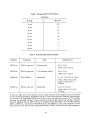
7
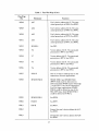
Table 2 User Wire-Wrap Pins
Wire-Wrap
Pin
Function
Mnemonic
WPI
SPARE 0
Spare input to the vector address multiplexer. This input can be used to read
part of a control/status register.
WP2
SPARE 3
See WPI.
Ground for vector address bit V3. See
WP23.
WP3
WP4
SPARE I
See WPI.
WP5
V2
Vector address bit 02.
WP6
ENB CLKAH
ENB CLK A H is the clock inpu t to the
Enable A Flip-Flop of the A interrupt
logic. When ENB CLK A H goes high,
ENB DATA A is clocked into the
Enable A Flip-Flop.
WP7
SPARE 2
See WPI.
WP8
ENB B STH
ENB B ST H is the status output from
the Enable B Flip-Flop of the B interrupt logic. When ENB B ST H is high,
the Enable B Flip-Flop is set.
WP9
IAKI L
Test point for the BIAK I bus signal.
BIAKI L is the processor's response to
BIRQ L and is daisy-chained such that
the first requesting device blocks the
signal propagation. Nonrequesting
devices pass the signal on as BIAKO L.
The leading edge of BIAKI L causes
BIRQ L to be un asserted by the requesting device.
WPIO
DOlL
Test point for data/address bit one.
Useful when testing the protocol logic.
DOl is latched in the protocol logic at
the asserted edge of BSYNC L. DO I and
D02 are decoded to produce the SEL DEV
outputs.
8
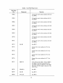
Table 2 User Wire-Wrap Pins (Cont)
Wire-Wrap
Pin
Function
Mnemonic
WP11
BWTBT L
Test point for the BWTBT bus signal,
while BDOUT L is asserted, BWTBT L
indicates a byte or word operation:
BWTBT L asserted indicates byte operation; BWTBT L un asserted indicates word
operation. BWTBT L decoded with
BDOUT Land BDAL 0 L forms OUT
LB L or OUT HB L.
WP12
RXCX
Test point for monitoring the delay of
BRPLY.
WP13
BSYNC H
Test point for the BSYNC L bus signal.
BSYNC L indicates that the address is
valid. At the assertion of BSYNC L,
address information is trapped in four
latches. While unasserted, disables all
outputs except the vector term of
BRPLY L. BSYNC L is held throughout
the entire bus cycle.
WP14
DOOH
One of 16 data or address lines from the
transceivers for user applications. Address
bit 00 is used for byte selection: 0 = low
byte; 1 = high byte.
WP15
BDOUT L
Test point for the BDOUT L bus signal.
BDOUT is a strobe signal to effect a
data output transaction. BDOUT L is
decoded with BWTBT Land BDALO to
form OUT LB L and OUT HB L.
BDOUT L also causes BRPLY L to be
issued through the delay circuit.
WP16
INWDL
In Word (IN WD) is used to gate input
data from a selected register onto the
LSI-II bus. Enabled by BSYNC Land
strobed by BDIN L.
WP17
D01H
One of 16 data or address lines from the
transceivers for user applications.
WP18
INIT 0 L
An initialize signal (asserted low) for
user applications.
WPl9
INIT 0 H
An initialize signal (asserted high) for
user applications.
9
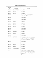
Table 2 User Wire-Wrap (Cont)
Wire-Wrap
Pin
Function
Mnemonic
WP20
BRPLY L
Test point for the BRPLY L bus signal.
BRPLY L is generated by VECTOR H
(vector term), or by BSYNC and ENB
in combination with either BDIN L, or
BDOUT L. Capacitor C37 can be added
by the user to ex tend the delay.
WP21
VEC RQSTB H
Used to distinguish whether device A or
device B is making a request. VECT
RQST B H is asserted for device B
requests and unasserted for device A
requests.
WP22
RQST AH
When RQST A H is asserted, the bus
request flip-flop for device A in the
interrupt logic is enabled, and BIRQ L
becomes asserted if the interrupt enable
flip-flop is set.
WP23
V3
Vector address bit 03. WP23 is used to
select the state of vector address bit 03.
When not wrapped to a ground pin,
vector address bit 03 is a "one." When
wrapped to WP3, vector address bit 03
is a "zero."
WP24
ENBDATAAH
Interrupt enable A data line. The level
on this line, in conjunction with the
ENB CLK A H (see WP6) line, determines the state of the A interrupt enable
flip-flop within the interrupt logic.
WP25
BIAKO L
Test point for the BIAKO L bus signaL
BIAKO L is the daisy-chained signal that
is passed by all devices not requesting
interrupt service (see WP9).
WP26
ENB CLK B H
ENB CLK B H is the clock input to the
enable B flip-flop of the B interrupt
logic. When ENB CLK B H goes high,
ENB DATA B is clocked into the enable
B flip-flop.
WP27
ENB DATAB H
Interrupt enable B data line. The level
on this line, in conjunction with the ENB
CLK B H (see WP26) lines, determines
the state of the B interrupt enable flipflop within the interrupt logic.
10
Table 2 User Wire-Wrap (Cont)
Wire-Wrap
Pin
Mnemonic
Function
WP28
RQST B H
When RQST B H is asserted, the bus
request flip-flop for device B in the interrupt logic is enabled, and BIRQ L
becomes asserted if the interrupt enable
flip-flop is set.
WP29
VECTORH
Test point for VECTOR H. This signal
causes BRPLY L (vector term) to be
generated through a delay independent of BSYNC Land ENB H.
VECTOR H also gates the vector
address onto the LSI-II bus via the
vector address generator.
WP30
D02 L
Test point for data/address bit two.
Useful when testing the protocol logic.
D02 is latched at the asserted edge of
BSYNC L. D02 and DO 1 are decoded to
produce the SEL DEV outputs.
WP31
ENBH
Test point for ENB H. This signal is the
result of a compare between the device
address on the LSI-II bus and the
device address established by the user.
When the addresses compare, ENB H is
asserted and sent to the protocol logic.
WP32
SEL DEV 6 L
One of four select signals that is true as
a function of BDALl Land BDAL2 L
if ENB H (see WP31) is asserted at the
asserted edge of BSYNC L. The four
select signals indicate that a user's register has been selected for a data transaction. The select signals remain asserted
until BSYNC L becomes unasserted.
WP33
SEL DEV 4L
See WP32.
WP34
SEL DEV 2L
See WP32.
WP35
SEL DEV OL
See WP32.
WP36
OUT LB L
Out Low Byte is used to load (write) data
into the low byte of a selected user
register. See WP3 7.
11
Table 2 User Wire-Wrap (Cont)
Wire-Wrap
Pin
Function
Mnemonic
WP37
OUTHB L
Out High Byte is used to load (write)
data into the high byte of a selected user
register. If used with OUT LB L, the
higher, lower, or both bytes can be
written. OUT HB L is enabled by
BSYNC L and the decode of BWTBT L
and BDALO L, and strobed by BDOUT L.
WP38
BIRQL
Test point for the BIRQ L bus signal.
This signal is asserted by a device needing
interrupt service.
WP39
BDMGOL
This signal is generated by DMA devices
as a result of arbitrating the BDMGI L
line. Jumper W2 must be removed if the
DRVII-P is to be used for DMA service.
WP40
BDMGIH
Used as a source for the BDMGI signal
to drive the user's DMA request arbitration logic. See WP3 9.
WP41
ENBASTH
ENB A ST H is the status output from
the enable A flip-flop of the A interrupt
logic. When ENB A ST H is high, the
enable A flip-flop is set.
WP42
Al2
Used to select the user's device address
along with WP45, 44, 43, 47, 48, 46,51,
49, 50. When not wrapped to a ground
pin, the particular device address bit will
be a "one." When wrapped to a ground
pin (WP62 for bit A 12), the particular
bit will be a "zero."
WP43
A09
User's device address bit 09. The associated ground pin is WP63. See WP42.
WP44
AIO
User's device address bit 10. The associated ground pin is WP64. See WP42.
WP45
All
User's device address bit 11. The associated ground pin is WP65. See WP42.
WP46
A06
User's device address bit 06. The associated ground pin is WP66. See WP42.
WP47
A08
User's device address bit 08. The associated ground pin is WP67. See WP42.
12
Table 2 User Wire-Wrap (Cont)
Wire-Wrap
Pin
Function
Mnemonic
WP48
A07
User's device address bit 07. The associated ground pin is WP68. See WP42.
WP49
A04
User's device address bit 04. The associated ground pin is WP69. See WP42.
WPSO
A03
User's device address bit 03. The associated ground pin is WP70. See WP42.
WPSI
AOS
User's device address bit OS. The associated ground pin is WP71. See WP42.
WPS2
SPARE 4
See WPI.
WPS3
V4
Vector address bit 03. The associated
ground pin is WP73. See WP23.
WPS4
V7
Vector address bit 07. The associated
ground pin is WP74. See WP23.
WPSS
VS
Vector address bit OS. The associated
ground pin is WP7S. See WP23.
WPS6
V6
Vector address bit 06. The associated
ground pin is WP76. See WP23.
WPS7
IN03 H
One of 16 data or address lines to the
transceivers for user applications.
WPS8
SPARE ENB 0
SPARE ENB 0 and SPARE ENB I
(WPS9) both must be driven low to
write data from SPARE inputs 0 through
7 to the LSI-II bus via the transceiver.
For 8-bit input applications, SPARE
ENB 0 could be driven by one of the
SEL DEV lines, while SPARE ENB 1
could be driven by IN WD L.
WPS9
SPARE ENB 1
See WPS8.
WP60
INOOH
See WPS7.
WP61
D09H
See WP17.
WP62
Ground for user's device address bit A 12.
See WP42.
WP63
Ground for user's device address bit A09.
See WP42.
13
Table 2 User Wire-Wrap (Cont)
Wire-Wrap
Pin
Mnemonic
Function
WP64
Ground for user's device address bit Al O.
See WP42.
WP65
Ground for user's device address bit All.
See WP42.
WP66
Ground for user's device address bit A06.
See WP42.
WP67
Ground for user's device address bit A08.
See WP42.
WP68
Ground for user's device address bit A07.
See WP42.
WP69
Ground for user's device address bit A04.
See WP42.
WP70
Ground for user's device address bit A03.
See WP42.
WP7I
Ground for user's device address bit AOS.
See WP42.
WP72
D04H
See WPI7.
WP73
Ground for vector address bit V 4. See
WP23.
WP74
Ground for vector address bit VS. See
WP23.
WP75
Ground for vector address bit V6. See
WP23.
WP76
Ground for vector address bit V7. See
WP23.
WP77
BBS7H
Test point for the Bank 7 Select (BBS7)
bus signal. This line is asserted by the
bus master when an address in the upper
4K bank (28-32K range) is placed on the
LSI-II bus.
WP78
SPARE 6
See WPI.
WP79
D02H
See WPI7.
WP80
IN 02H
See WPS7.
14
Table 2 User Wire-Wrap (Cont)
Wire-Wrap
Pin
Mnemonic
Function
WP81
DIS H
See WP17.
WP82
IN 13 H
See WP57.
WP83
D14H
See WP17.
WP84
D13 H
See WPI7.
WP85
D12H
See WPI7.
WP86
IN 12 H
See WP57.
WP87
D03H
See WP17.
WP88
D07H
See WP17.
WP89
IN IOH
See WP57.
WP90
SPARE 7
See WP1.
WP91
DlOH
See WP17.
WP92
IN 09 H
See WP57.
WP93
NOT USED.
WP94
TRANS ENB C L
Enables user's data to be placed onto the
LSI-II bus. Both TRANS ENB C and A
(WP94 and WP 120) and TRANS ENB D
and B (WP95 and WP 100) must be
driven low prior to the processor's
read data time.
WP95
TRANS ENB D L
See WP94.
WP96
IN 01 H
See WP57.
WP97
VECENBH
Test point for VEC ENB H. This signal
gates the vector address to the LSI-II
bus, provided that jumper W4 has not
been removed. WP97 can be used as the
source for VEC ENB H when adding an
additional gate to the DRVI1-P for
vector address expansion up to 774 8 .
WP98
IN 06 H
See WP57.
WP99
IN04H
See WP57.
15
Table 2 User Wire-Wrap (Cont)
Wire-Wrap
Pin
Mnemonic
WPIOO
TRANS ENB B L
See WP94.
WPIOI
IN IS H
See WPS7.
WP102
IN 14 H
See WPS7.
Function
WPI03
Used to pull-up the VEC ENB H line
when jumper W4 is removed.
WPI04
NOT USED.
WPIOS
NOT USED.
WPI06
D08H
See WPI7.
WPI07
D06H
See WPI7.
WPI08
IN II H
See WPS7.
WPI09
DII H
See WPI7.
WPIIO
NOT USED.
WPIII
NOT USED.
WPI12
SPARE 5
See WPI.
WPI13
IN 08H
See WPS7.
WPI14
WPIIS
NOT USED.
BSYNCH
WPI16
Test point for BSYNC H. At the asserted
edge of this signal, address information
is trapped'in four latches. BSYNC H is
the inversion of BSYNC L. See WPI3.
NOT USED.
WPI17
DOSH
See WPI7.
WPI18
IN 07H
See WPS7.
WPI19
IN 05 H
See WPS7.
WPI20
TRANS ENBAL
See WP94.
+3V
There are two +3V source wire-wrap
pins on the DRVII-P. Each +3V source
can drive up to 13 TTL unit loads. These
sources can be used for pulling-up unused
TTL inputs.
16
Vector Address Selection
Vector addresses 0-7748 are reserved for users of the LSI-II system. As manufactured, the DRVII-P
can vector address in the range from 0-3748. However, by adding one gate to the DRVII-P vector
address logic, the user can extend the vector address to 774 8 . The user selects the interrupt vector
address by means of wire-wrap pins (WP) on the DRVII-P module.
Figure 4 shows the vector address select format and presents the wire-wrap pin-to-bit relationship for
vector address selection. Bits to be decoded as "ZERO" bits in the vector address are wire-wrapped to
ground wire-wrap pins (WP). Bits to be decoded as "ONE" bits are left unwrapped as these bits are
pulled-up to the one state.
1ST
OCTAL
DIGIT
2 NO
OCTAL
DIGIT
A
,.-----A---, I
OB
07
r--I
BIT OB AVAILABLE
FOR EXTENDED
ADDRESSING.
SEE TEXT.
06
04
05
LEAST
SIGNIFICANT
OCTAL PREASSIGNED
DIGIT
AS
(0 OR 4)
ZEROS
~
03
02
01
00
I
"'IL ___
WP
54
WP
56
WP
55
WP
53
WP
23
WIRE-WRAP
TO A GROUND
WP FOR "ZERO"
BITS IN THE
ADDRESS
WP
5
(SEE TEXT)
WP
74
WP
76
WP
75
WP
73
WP
23
~rL
FROM INTERRUPT LOGIC
tI-4154
Figure 4 DRVII-P Vector Address Select Format
It is recommended that WP5 (vector bit 02) be wrapped to WP21 (VEC RQST B H). This will
automatically decode the least significant bit of the vector address as a 0 or a 4. When the VECTOR H
signal is issued as a result of the B half of the interrupt logic becoming bus master, the VEC RQST B H
(WP5) signal is also issued changing bit 02 of the vector address, thus presenting a different vector
address for interrupt B.
The VEC RQST B H line can be thought of as a one bit code indicating which half of the interrupt
logic is bus master. When bit 02 of the vector address is a zero, the A half is bus master; a one indicates
that the B half is master.
Bus Receivers
All LSI-II bus data and control lines are fully buffered on the DRVII-P module. Buffering for the
data and address lines (BDAL) is accomplished by the bus transceivers. Bus control lines (BWTBT,
BDOUT, BDIN, BSYNC, BBSY, BIAKI, and BDMGI) are buffered on the DRVII-P with type 8640
bus receivers. These receivers are high impedance receivers with the following input levels:
High
Low
=
=
1.7V min.
1.3V max.
The receivers have standard TTL compatible outputs which are made available (for most bus signals)
to the user by means of wire-wrap pins (WP). The bus signals and the associated wire-wrap pins for
user application are listed and defined in Table 2.
17
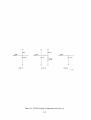
+3V Source
There are two +3V wire-wrap pins (Figure 2, sheet 2) on the DRVll-P module. These pins provide a
source of +3V for pulling-up unused TTL inputs. Each +3V source is capable of driving up to 13 TTL
unit loads. The +3V sources are derived from resistor dividers placed across the +5V logic source.
USER I/O LINES AND ASSOCIATED WIRE-WRAP PINS (WP)
There are 112 user I/O lines and 122 wire-wrap pins (not counting the 40-pins for the I/O connector
and the 70-pins for C and D module fingers) for user applications. A functional description of the user
I/O lines was presented in the Functional Description paragraphs. All user I/O lines are TTL
compatible and are listed and described in Table 2 along with the associated wire-wrap pin (WP).
LSI-II bus signals are not included. A description of the bus signals can be found in the LSI-II
PDP-l 1/03 User's Manual.
PHYSICAL DESCRIPTION
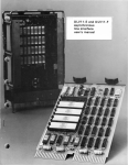
Figure 5 shows the physical layout of the DRVll-P. There are 12 vertical user areas for IC placement.
User area "A" can accommodate ICs with pins on 0.3 in. (0.762 cm), 0.4 in. (1.01 cm), and 0.6 in.
0.52 cm) centers. This first area can be dedicated to any IC or IC sockets with the above mentioned
pin centers, or a mixture of ICs with those pin centers can be installed.
User areas "B" through "L" and area "N" can accommodate ICs or IC Sockets with 0.3 in. (0.762 cm)
pin centers. Whereas area "M" can accommodate ICs or IC Sockets with 0.3 in. (0.762 cm) and/or 0.4
in. (1.01 cm) pin centers.
As an aid to exact location of wire-wrap pins and IC connections, each vertical column is assigned an
alphabetic designation and each horizontal row is assigned a numeric designation. A specific wire-wrap
pin can be specified by referring to column A through L and row 1 through 64. In the same way, an IC
connection can be specified by referring to column M through CC and row 1 through 31.
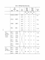
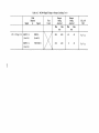
The maximum ICs which the DRVII-P can accommodate is listed in Table 3.
User areas "A," "B," "C," and "E" are equipped with a ground wire-pin (-) and a +5V wire-wrap pin
(+) at both ends of each column of wire-wrap pins. These ground and +5V pins are to be used for
supplying +5V and ground to the user's logic. The capacitors above (C36, C34, C32, C30, and C28)
and below (C35, C33, C3l, C29 and C27) the user areas provide decoupling for the +5V source.
Additional decoupling capacitors can be added by the user as required.
User areas "F" through "N" only have ground (-) and +5V (+) wire-wrap pins at the lower end of each
column of wire-wrap pins. Capacitors C26 through C20 provide the +5V decoupling for these user
areas.
A 40-pin connector is provided in the upper right of the DRVll-P module. This connector can be used
as an I/O connector for interfacing to a user's I/O device. Each connector pin is brought to a wire-wrap
pin on the module. Module wire-wrap pins are designated the same as the connector pins. Figure 5
shows the designations for all the connector wire-wrap pins. The actual module only has designations
for pins A and UU. Three wire-wrap pins to the right of the 40-pin connector are ground pins and can
be used for cable grounds.
Table 4 lists cables, available from Digital Equipment Corporation, which have 40-pin connectors that
mate with 11 on the DRVI1-P. Standard length cables are listed. Non-standard lengths may be ordered
at additional cost. Contact the nearest Digital Equipment Corporation Sales Office for prices and
availability. The desired cable length (xx) must be specified when ordering.
18
+5V WIRE-WRAP PIN
UPPER RIGHT
PIN OF FIRST
FIVE MOUNTING
AREAS
FH
GROUND WIRE-WRAP PIN
UPPER LEFT
PIN OF FIRST
FIVE MOUNTING
AREAS
WIRE-WRAP PINS
FOR INTERCONNECTING
USER Ie's
··
25:·
···
20:
30.
E
u
N
\0
E
":
..:
c::::.
~ --....!-
~U
~
~ii:
~
USER WIRE-WRAP
PINS FOR CONNECTING
USER LOGIC TO "C"
AND" D" DRVlI-P
MODULE FINGERS
u
N
W
.
~
• Ul
.: a::
• •
__ :-! __
":
•
.L. . . ~
::
ci
i=
~
-z
(/) -
.(/)
u E
u
:
:
(f)
HUH
••
U
H
a:
••
a:
~~
IJ..-
:.
<to
•
W~
~ci
0::
~~
:)«
~
«
::
::
W
~
a::.. .
~
~
:•
[TID \ :+
•••••
~
«
W
~W
-
NP
E
W
J:W
GROUND WIRE-WRAP PIN
LOWER LEFT
PIN OF ALL
MOUNTING
AREAS.
DESIGNATED
BY MINUS (-)
SIGN.
LM
u
N
W
ci~
-
JK
v
o
",W
+5V WIRE-WRAP PIN
LOWER RIGHT
PIN OF ALL
MOUNTING
AREAS.
DESIGNATED
BY PLUS (+)
SIGN.
THREE WIRE-WRAP PINS
FOR ACCOMMODATING
CABLE GROUNDS
WIRE-WRAP PINS FOR CONNECTING
USER LOGIC TO 40-PIN CONNECTOR
~-::---i+-~
···
......
..
......
• 101
• • _81
· ..........
~
..
..
.
a::
,M'ca
~
3V
•. ""'~
mD··@I]··@D··@D·
++++
• • • • • • • • • • • ~Wl • • • • • • • • • • • • • • • • • •
(\JNNN NN NNNNNNNNNNNN
>:l ..... UI a:::a.. Z::E...J:!I:::-,J:IL.WOUCD«
C\lNNN NC\I NNNNNNNNNNNN
>:>I-UI Ira.. Z::E...J~"'J:1L.WOUID«
................iD:t
;;;;;;;ro::Zi~~':; i~wou
~
W
W
....
....
........
..........
..
'"
W
~----..;.;~---......-
00 ~
..
BO __ 60
~ ~ ~
G
8~
8
REMOVE TO DISABLE
VECTOR ADDRESSING
(SEE TEXT)
USER WIRE-WRAP
;...- - - 4 - ~~~~:iD FROM
1 TH ROUGH 120
................. .
;:;~U;a:~zi:;~:; I~WOU
c
BIAKI L - BIAKO L
CONTINUITY JUMPER.
REMOVE ONLY WHEN
USING THE CN2 AND
CM2 MODULE FINGERS.
w
'"
+3V WIRE-WRAP PIN
FOR PULLING-UP
UNUSED GATE
INPUTS, ETC.
BDMGI L - BDMGO L
CONTINUITY JUMPER.
REMOVE ONLY WHEN
USING THE CR2 AND
(S2 MODULE FINGERS.
iii;;
A
B
+3V WIRE-WRAP PIN
FOR PULLING-UP
UNUSED GATE
INPUTS, ETC.
BDMGI L - BDMGO L
CONTINUITY JUMPER.
REMOVE ONLY Wrl EN
DMA GRANT ARBITRATION
LOGIC IS CONSTRUCTED
ON DRVlI-P MODULE.
SPLIT LUGS TO ACCOMMODATE
EXTERNAL CAPACITOR (C39) WHEN
ADJUSTING DELAY BETWEEN
BDIN L, BDOUT L, AND
BETWEEN VECTOR H INPUTS
AND BRPLY L.
11-4152
Figure 5 DRVll-P Physical Layout
Table 3 Maximum DRVII-P IC Density
(All Areas)
IC Type
Max.ICs
6 pin
122
8 pin
97
14 pin
61
16 pin
52
18 pin
44
20 pin
43
22 pin
6
24 pin
5
40 pin
3
Table 4 Recommended Cable Assemblies
Type
Length (ft./m.)
Cable No.
Connectors
BC07A-xx
H856 to open end
20-twisted pair
10, 15,25 ft.
3.050,4.575, 7.625 m.
BC07D-xx
H856 to open end
2, 20-conductor ribbon
10, 15,25 ft.
3.050,4.575, 7.625 m.
BC08R-xx
H856 to H856
Shielded flat
1,6, 10, 12,20,50, 75, 100 ft.
0.305, 1.830,3.050,3.660,
6.100, 15.250, 22.875,
30.500 m.
BC04Z-xx
H856 to open end
Shielded flat
6, 10, 15,25,50ft.
1.830,3.050,4.575, 7.625,
15.250 m.
In the lower right area of the module are the ICs which constitute the bus interface logic (as described
in the Functional Description paragraphs) and the 122 user wire-wrap pins. These user wire-wrap pins
are the sources for logic signals which are to be used to drive the user's logic circuits. All 122 wire-pins
are listed and described in Table 2. Also contained in the lower right area are two split lugs. Capacitor
C39 (not supplied with the DRVl1-P) can be soldered across these lugs to vary the delay between
BDIN L, BDOUT L, and between VECTOR H inputs and BRPLY L if the normal tolerance for this
delay does not meet with the user's requirements (refer to Table 1 and the Protocol Logic paragraph).
20
Jumpers W2 and W4 are also contained in this area of the module. W2 provides BDMGI Land BDMGO
L continuity for the LSI-II bus. This jumper should be removed only if the user constructs a DMA
(direct memory access) interface on the DRVII-P and DMA grant arbitration logic is included. W4
enables or disables vector addresses. With W4 installed, a vector address will automatically be placed
onto the bus when an interrupt is generated. If W4 is removed and WPI03 is wire-wrapped to a ground
wire-wrap pin, the DRVII-P will interrupt but will not place a vector address onto the bus.
The last module area to be discussed is the area directly above module fingers C and D. This area
contains jumpers WI and W3. WI should be removed only if the user constructs circuitry on the
module which uses the BIAKO L (finger CN2) and BIAKI L (finger CM2) lines of the C and D bus
slots. W3 should be removed if the BDMGO L (finger CS2) and BDMGI L (finger CR2) lines of the C
and D bus slots are used. The balance of this area is dedicated to user wire-wrap pins for the C and D
fingers. As indicated in Figure 5, these wire-wrap pins have a one-to-one correlation with the C and D
module fingers.
All wire-wrap pins accept 30-gauge wire and there are two holes in the DRVII-P module which can be
used for custom mounting of the module. One hole is in the approximate center of the module, while
the second is to the left of the 40-pin connector.
MODULE INSTALLATION
With the exception of the first slot (the LSI-ll processor always occupies the first slot), the DRVI1-P
can be installed into any four slots of the LSI-II backplane. However, if the DRVII-P is configured as
a DMA module and if an REVll DMA refresh option is used, the DRVII-P must be at a lower
priority than the REVIl. When inserting the module into the backplane, make sure that the deep
notch on the module seats against the connector block rib. Do not insert or remove the module with
power applied. Connect the user I/O cables to J1 on the DRVII-P.
WIRE-WRAP TOOLS
The wire-wrap pins (WP) used on the DRVII-P are sized for 30-gauge wire and wire-wrap accessories.
Table 5 lists 30-gauge wire-wrap tools which can be purchased from Digital Equipment Corporation.
Contact the nearest Digital Equipment Corporation Sales Office for prices and availability.
Table 5 Wire-Wrap Tools
Part No.
Description
HSIO-A
Pistol grip mechanical wire-wrap tool for 30-gauge wire.
HSIO-D
Battery powered wire-wrap gun for 30-gauge wire.
H811-A
Hand wire-wrap tool for 30-gauge wire.
H812-A
Hand unwrapping tool for 30-gauge wire.
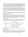
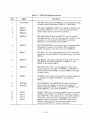
DRVII-P PARTS LIST
Table 6 lists the parts supplied with the DRVII-P option by part number, description, and quantity.
RELATED LITERATURE
In addition to the data contained in this manual, the LSI-II PDP-I 1/03 User's Manual and the LSI-II
PDP-l 1/03 Processor Handbook contain useful information on interface circuits as well as installing
and operating interface module such as the type which the user might configure on the DRVII-P.
Handbooks may be ordered from the nearest Digital Equipment Corporation Sales Office.
21
Table 6 DRVII-P Parts List
Part No.
Description
M7948
LSI-II Foundation Module
MPOOl19
Field Maintenance Print Set
EK-DRVII-OP-OOI
DRVII-P Foundation Module User's Manual
22
Quantity
I Set
APPENDIX A
IC DESCRIPTIONS
The special purpose ICs designed and manufactured by Digital Equipment Corporation and used in the
DRVII-P are described in this Appendix. These ICs are the DC003 interrupt logic and the DC004
protocol logic. A brief description of each IC, the signal lines, IC pinning, a timing diagram, and a
simplified logic diagram are supplied.
A.1 DC003 INTERRUPT LOGIC
The interrupt chip is an IS-pin, 0.300" center, DIP device that provides the circuits to perform an
interrupt transaction in a computer system that uses a "pass-the-pulse" type arbitration scheme. The
device is used in peripheral interfaces and provides two interrupt channels labeled "A" and "B," with
the A section at a higher priority than the B section. Bus signals use high-impedance input circuits or
high-drive-open-collector outputs, which allows the device to directly attach to the computer systems
bus. Maximum current required from the Vcc supply is 140 rnA.
Figure A-I is a simplified logic diagram of the DC003 IC. Timing for the "A" interrupt section is
shown in Figure A-2, while Figure A-3 shows the timing for both "A" and "B" interrupt sections.
Table A-I describes the signals and pins of the DC003 by pin and signal name.
A.2 DC004 PROTOCOL LOGIC
The protocol chip is a 20 pin 0.300" center, DIP device that functions as a register selector, providing
the signals necessary to control data flow into and out of up to four word registers (S bytes). Bus
signals can directly attach to the device because receivers and drivers are provided on the chip. An RC
delay circuit is provided to slow the response of the peripheral interface to data transfer requests. The
circuit is designed such that if tight tolerance is not required, then only an external I K ±20 percent
resistor is necessary. External RC's can be added to vary the delay. Maximum current required from
the V cc supply is 120 rnA.
Figure A-4 is a simplified logic diagram of the DC004 IC. Signal timing with respect to different loads
are tabularized in Table A-2 and are shown in Figure A-S. Figure A-6 shows the loading for the test
conditions in Table A-2. Signal and pin definitions for the DC004 are presented in Table A-3.
A-I
+VCC--§I
+VCC
.----------------------------------------------------------------------------------------------i16ENAST H
RCSTA H
ENOATA H
VECTOR H
VECROSTB H
BOIN L
INITO L
BINIT L
BIAKO L
BIAKI L
BIRO L
GNO
'r---------~~~--~O
ENACLK H 14·1-----bC
0
CLR
C
0
CLR
VCC
ROSTAH
ENAST H
ENAOATA H
ENACLK H
ENBCLK H
ENBOATAH
ENBST H
ROSTB H
6
7
BIAKI L 071---------+-----a
)O"'-----I---,-------+------~,06I BIAKO L
BOIN L
L-~--t-----_r~o_--~--------_+--~--_+------~~BIRO
§
L
ENOST H
SET
ENOOATA H 121------10
ENBCLK H
o
131-----I>C
0
CLR
1
C
o
O~----------_r_
VECROSTB H
CLR
+VCC
ROSTO H
IO~------~----------~
~GNO
L--+---I>C
0
CLR
IK
L---------------------~L-----------------------~--------L------------L------------------~INIroL
Figure A-I DC003 Simplified Logic Diagram
BINIT l - - ,
~.<?.<? 1300
:
~MINI
I
I
I
I
INITO l
7~5 --~I- - - - - - - - - - - - - - - - - - - - - - - - - - - - - - - - - - - - - - - - - - - - - - - - - - - - - - - - - - - - - - - - - --+i
I
~
I
I
I
I
ENA DATA H
I
I
I
ENA ClK H
30MIN~ ~L____________________________~r__lL___________________________
I
I
ENA ST H
7-30~
F
RQSTA H
BIRQ l
I
15-65-+,
I
r-. __
--'......,:""""""F 20 - 90
BDIN l
I
BIAKI l
35 M I N _
I
I
VECTOR H
35 MIN_
I
I
I
I
I
I
10-45-:
I
I
F~
q
I
I
r-
I
I
10 - 45
I
I
I
I
12-55 --:
BIAKO l
W=12-55
I
NOTE:
Times ore in nanoseconds
11-4150
Figure A-2 DC003 "A" Interrupt Section Timing Diagram
A-3
BIN IT L
~OO
300
MIN MIN
:I
I
I
I
'II
~
I
I
INITO L 7-35
I
12-50
I
I
I
ENB DATA H
I
I
ENB CLK H
30 MIN
--1 Fl
I
I
I
ENB ST H
7-30
BIRO L
--!
L-___________________________________________________________
F
15-65-1
I
I
r:
~----------------------------------------------------
ROSTB H
ENA DATA
H
I
I
I
ENA CLK H
30 MIN--1
F
ENA ST H
ROSTA H
B DIN L
35 MIN---l
BIAKI L
I
~
I
I
I
I
35 MIN - - ;
1-7=_---..J1
r--
I
, :
LJ"-i::-J
~
:-1L'_0_-_4_5_________'_0_-_45_f--I~
VECTOR H ________________________________1_0_-_4_5!..!1..J
VECROSTB H
I
I:::J
:-1
'0- 45
I
I
I
H
15-65::--:1
I
15-65
NOTE:
Times are in nanoseconds
11-4151
Figure A-3 De003 "A" and "B" Interrupt Sections Timing Diagrams
A-4
Table A-I
Pin
DC003 Pin/Signal Descriptions
Description
Signal
VECTORH
INTERRUPT VECTOR GATING SIGNAL. This signal should
be used to gate the appropriate vector address onto the bus
and to form the bus signal called BRPLY L.
2
VEC RQSTBH
VECTOR REQUEST "B" SIGNAL. When asserted indicates
RQST "B" service vector address is required. When un asserted
indicates RQST "A" service vector address is required.
VECTOR H is the gating signal for the entire vector address:
VEC RQST B H is normally bit 2 of the vector address.
3
BDINL
BUS DATA IN. This signal generated by the processor BDIN
always preceeds a BIAK signal.
4
IN ITO L
INITIALIZE OUT signal. This is the buffered BINIT L signal
used in the device interface for general initialization.
5
BINIT L
BUS INITIALIZE signal. When asserted, this signal brings all
driven lines to their unasserted state (except IN ITO L).
6
BIAKO L
BUS INTERRUPT ACKNOWLEDGE signal (OUT). This
signal is the daisy-chained signal that is passed by all devices
not requesting interrupt service (see BIAKI L). Once passed
by a device, it must remain passed until a new BIAKI L is
generated.
7
BIAKI L
BUS INTERRUPT ACKNOWLEDGE signal (IN). This signal
is the processor's response to BIRQ L true. This signal is
daisy-chained such that the first requesting device blocks the
signal propagation while non-requesting devices pass the
signal on as BIAKO L to the next device in the chain. The
leading edge of BIAKI L causes BIRQ L to be un asserted by
the requesting device.
8
BIRQL
ASYNCHRONOUS BUS INTERRUPT REQUEST from a
device needing interrupt service. The request is generated by
a true RQST signal along with the associated true interrupt
enable signal. The request is removed after the acceptance of
the BDIN L signal and on the leading edge of the BIAKI L
signal or the removal of the associated interrupt enable or due
to the removal of the associated request signal.
REQSTBH
REQSTAH
DEVICE INTERRUPT REQUEST SIGNAL. When asserted
with the enable "A" flip-flop asserted will cause the assertion
of BIRQ L on the bus. This signal line normally remains
asserted until the request is serviced.
10
17
A-5
Table A-I DC003 Pin/Signal Descriptions (Cont)
Pin
11
Signal
Description
16
ENB ST H
ENASTH
INTERRUPT ENABLE "A" STATUS signal. This signal indicates the state of the interrupt enable "A" internal flip-flop
which is controlled by the signal line ENA DATA H and the
ENA CLK H clock line.
12
15
ENB DATA H
ENADATAH
INTERRUPT ENABLE "A" DATA signal. The level on this
line, in conjunction with the ENA CLK H signal, determines
the state of the internal interrupt enable "A" flip-flop. The
output of this flip-flop is monitored by the ENA ST H signal.
13
14
ENBCLKH
ENACLKH
INTERRUPT ENABLE "A" CLOCK. When asserted (on the
positive edge), interrupt enable "A" flip-flop assumes the
state of the ENA DATA H signal line.
A-6
VECTOR H
BDAl2 l
BDALI l
BDAlO l
BWTBT l
BSYNC l
BDIN l
BRPlY l
BDOUT l
GND
VCC
ENB H
RXCX H
SEl6 l
SEl4 l
SEl2 l
SElO l
OUTHB l
OUTlB l
INWD l
~"",,"-+VCC
ENB H
19I---L-----~D
ll-------r--------------,
~ vcc
ENB
lATCH
BSYNC l
"":>o>--.-4G
BDAl2 l
21------+-~D
a
@}----
GND
1
02
LATCH
Or-_ _ _~-------------~D~A~l~2~
G
SEl6 L
DECODER
SEl4 L
BDAll l
D3,1------+-~D
1
SEL 2 L
Ot
LATCH
G
OI-_ _ _~----------------~D~A~l~l~
SEL
al
BDAlD L 104~-----4--4D
00
OUTHB L
t==jI~~----------------_+--_F=;~------------~
LATCH
G
O'~------4-----~~
DUTLB L
RXCX H
BRPLY L
BDOUT L
VECTOR H
BDIN L
INWD L
IC-0174
Figure A-4 DC004 Simplified Logic Diagram
Table A-2 DC004 Signal Timing vs Output Loading
Signal
-
With
Respect
to
Signal
Test
Condo
Output
Being
Asserted
Min
Max
(ns)
SEL (0,2,4,6) L
OUTLB L
OUTRB L
INWDL
Pin 18
Connection
RX = lK ±5%
350n ±5%
15 pf±5%
BSYNC L
BDOUT L
DBOUTL
BDINL
Output
Being
Asserted
Min
Max
(ns)
Load B
15
35
5
25
LoadC
15
40
5
30
Load B
5
25
5
25
LoadC
5
30
5
30
Load B
5
25
5
25
Load C
5
30
5
30
Load A
5
25
5
25
Load B
5
30
5
30
Fig. A-S
Ref.
t5' t6
t9, tlO
t9, tlO
t11, t12
BRPLY L
(Load A)
OUTLB L
(Load B)
20
60
-10
45
BRPLY L
OUTRB L
20
60
-10
45
(Load A)
(Load B)
BRPLY L
20
60
-10
45
t13' t14
(Load A)
INWDL
(Load B)
BRPLY L
VECTORR
30
70
0
45
t13' t14
300
400
-10
45
t13' t14
(Load A)
OUTLB L
(Load B)
BRPLY L
(Load A)
OUTRB L
(Load B)
300
400
-10
45
t13' t14
t13, t14
t13' t14
(Load A)
Pin 18
Connection
RX = 4.64K ±1%
BRPLY L
Table A-2 DC004 Signal Timing vs Output Loading (Cont)
Signal
CX = 220 pf±l%
With
Respect
to
Signal
Test
Condo
Output
Being
Asserted
Min
Max
(ns)
Output
Being
Asserted
Min
Max
(ns)
Fig. A-5
Ref.
BRPLYL
(Load A)
INWDL
(Load B)
300
400
-10
45
t13' t14
BRPLY L
(Load A)
VECTORH
330
430
0
45
t13' t14
BDAL (2,1,0) L
ENB
%0a25
MINI25
MIN~
H%W1J~N ~~N~
BSYNC L
SEL (0,2,4,6) L
BWBTL~
,
,
~
I
I
BDOUT L
OUTHB
15 MIN.-l
I
I
~'
j_;:-:~:-~----~~~~~-*----~~(I-('rj------- ~IL____
_____
15_M_'_N_.
,
,
-i,no I--
L-------------~'-,
---1
OUTLB L
-_-...,..
T9t=
~I------*----~.. I~--
BDIN L
I
I
IWD L
----------_____
--,
~T13t--:
,
,
~'
BRPLY L
~T12F
,I
,
T...1~t= 2.4V
-:
~------~,- - ' ,
I
I
,
I
I
I-
VECTOR H _ _ _ _ _ _ _ _ _ _ _ _ _ _......1
I
I
I
:
--l F
T15
* _----t..-II
--! Lt--:
_____---------T16
*TIMEREQUIREDTO DISCHARGE RxCxFROM ANY CONDITION ASSERTED=150ns
NOTE:
Times are in nanoseconds
11-4348
Figure A-5 DC004 Timing Diagram
A-IO
Vee
FROM
OUTPUT
+.
roo"
LOAD A
Vee
Vee
2BOn
FROM
OUTPUT
OU~~~~
r"
LOAD 8
)
DIODEFD777
1'' '
LOAD C
11-4349
Figure A-6 DC004 Loading Configurations for Table A-2
A-II
Table A-3 DC004 Pin/Signal Descriptions
Pin
Description
Signal
VECTORH
VECTOR. This input causes BRPL Y L to be generated through
the delay circuit. Independent of BSYNC Land ENB H.
3
4
BDAL2 L
BDALIL
BDALO L
BUS DATA ADDRESS LINES. These signals are latched at the
assert edge of BSYNC 1. Lines 2 and I are decoded for the
select outputs; line 0 is used for byte selection.
5
BWTBTL
BUS WRITE/BYTE. While the BDOUT L input is asserted,
this signal indicates a byte or word operation: Asserted = byte,
un asserted = word. Decoded with BOUT L and latched
BDALO L to form OUTLB Land OUTHB 1.
6
BSYNC L
BUS SYNCHRONIZE. At the assert edge of this signal, address
information is trapped in four latches. While unasserted,
disables all outputs except the vector term of BRPLY 1.
7
BDINL
BUS DATA IN. This is a strobing signal to effect a data input
transaction. Generates BRPLY L through the delay circuit and
INWD 1.
8
BRPLY L
BUS REPLY. This signal is generated through an RC delay by
VECTOR H, and strobed by BDIN L or BDOUT L, and
BSYNC L and latched ENB H.
9
BDOUTL
BUS DATA OUT. This is a strobing signal to effect a data
output transaction. Decoded with BWTBT Land BDALO to
form OUTLB Land OUTHB L. Generates BRPLY L through
the delay circuit.
11
INWDL
IN WORD. Used to gate (read) data from a selected register on
to the data bus. Enabled by BSYNC L and strobed by
BDIN 1.
12
13
OUTHBL
OUTLB L
OUT LOW BYTE, OUT HIGH BYTE. Used to load (write)
data into the lower, higher, or both bytes of a selected
register. Enabled by BSYNC L and decode of BWTBT Land
latched BDALO L, and strobed by BDOUT 1.
14
15
16
17
SELOL
SEL2L
SEL4L
SEL6L
SELECT LINES. One of these four signals is true as a function
of BDAL2 Land BDAL I L if ENB H is asserted at the assert
edge of BSYNC 1. They indicate that a word register has been
selected for a data transaction. These signals never become
asserted except at the assertion of BSYNC L (then only if
ENB H is asserted at that time) and once asserted, are not
unasserted until BSYNC L becomes unasserted.
2
A-12
Table A-3 DC004 Pin/Signal Descriptions (Cont)
Pin
Signal
Description
18
RXCX
EXTERNAL RESISTOR CAPACITOR NODE. This node is
provided to vary the delay between the BDIN L, BDOUT L,
and VECTOR H inputs and BRPLY L output. The external
resistor should be tied to VCC and the capacitor to ground.
As an output, it is the logical inversion of BRPLY L.
19
ENBH
ENABLE. This signal is latched at the asserted edge of
BSYNC L and is used to enable the select outputs and the
address term of BRPLY L.
A-13
Reader's Comments
DRVII-P FOUNDATION MODULE
USER'S MANUAL
EK-DRVII-0P-002
Your comments and suggestions will help us in our continuous effort to improve the quality and usefulness of
our publications.
What is your general reaction to this manual? In your judgment is it complete, accurate, well organized, well
written, etc.? Is it easy to use?
What features are most useful?
What faults do you find with the manual?
Does this manual satisfy the need you think it was intended to satisfy?
Does it satisfy your needs? _ _ _ _ _ _ _ _ __
Why? ______________________________________________________________________________
Would you please indicate any factual errors you have found.
Please describe your position.
Name
Street
Organiza tion
_______________________ Department
Ci ty ______________________________________
Sta te _____________________________________________________ Zip or Country
-----------~~-----------
-
-
-
-- -- -- -
-
DoNotTear-FoldHereandStaple
-
-
-
-
-
-
-
FIRST CLASS
PERMIT NO. 33
MAYNARD, MASS.
BUSINESS REPLY MAIL
NO POSTAGE STAMP NECESSARY IF MAILED IN THE UNITED STATES
Postage will be paid by:
Digital Equipment Corporation
Technical Documentation Department
Maynard, Massachusetts 01754
-