1
Technical Description
SunSpec® Modbus® Interface
SunSpec_Modbus-TB-US-en-14 | Version 1.4
ENGLISH
SMA America, LLC
Legal Provisions
Legal Provisions
Copyrightⓒ 2014 to 2015 SMA America, LLC. All rights reserved.
No part of this document may be reproduced, stored in a retrieval system, or transmitted, in any
form or by any means, electronic, mechanical, photographic, magnetic or otherwise, without the
prior written permission of SMA America, LLC.
Neither SMA America, LLC nor SMA Solar Technology Canada Inc. makes representations, express or implied, with respect to this documentation or any of the equipment and/or software it may
describe, including (with no limitation) any implied warranties of utility, merchantability, or fitness
for any particular purpose. All such warranties are expressly disclaimed.
Neither SMA America, LLC nor its distributors or dealers nor SMA Solar Technology Canada Inc.
nor its distributors or dealers shall be liable for any indirect, incidental, or consequential damages
under any circumstances.
(The exclusion of implied warranties may not apply in all cases under some statutes, and thus the
above exclusion may not apply.)
Specifications are subject to change without notice. Every attempt has been made to make this
document complete, accurate and up-to-date. Readers are cautioned, however, that
SMA America, LLC and SMA Solar Technology Canada Inc. reserve the right to make changes
without notice and shall not be responsible for any damages, including indirect, incidental or consequential damages, caused by reliance on the material presented, including, but not limited to,
omissions, typographical errors, arithmetical errors or listing errors in the content material.
All trademarks are recognized even if these are not marked separately. Missing designations do
not mean that a product or brand is not a registered trademark.
Modbus® is a registered trademark of Schneider Electric and is licensed by the Modbus Organization, Inc.
SMA America, LLC
3801 N. Havana Street
Denver, CO 80239 U.S.A.
SMA Solar Technology Canada Inc.
2425 Matheson Blvd. E, 7th Floor
Mississauga, ON L4W 5K4, Canada
2
SunSpec_Modbus-TB-US-en-14
Technical Description
SMA America, LLC
Important Safety Instructions
Important Safety Instructions
SAVE THESE INSTRUCTIONS
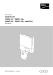
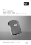
This manual contains important instructions for the following products:
•
SMA inverters with integrated Speedwire interface or with a retrofitted
Speedwire/Webconnect data module
This manual must be followed during installation and maintenance.
The product is designed and tested in accordance with international safety requirements, but as
with all electrical and electronic equipment, certain precautions must be observed when installing
and/or operating the product. To reduce the risk of personal injury and to ensure the safe installation and operation of the product, you must carefully read and follow all instructions, cautions and
warnings in this manual.
Warnings in this document
A warning describes a hazard to equipment or personnel. It calls attention to a procedure or practice, which, if not correctly performed or adhered to, could result in damage to or destruction of
part or all of the SMA equipment and/or other equipment connected to the SMA equipment or
personal injury.
Symbol
Description
DANGER Indicates a hazardous situation which, if not avoided,
will result in death or serious injury
WARNING Indicates a hazardous situation which, if not avoided,
could result in death or serious injury
CAUTION Indicates a hazardous situation which, if not avoided,
could result in minor or moderate injury
NOTICE Indicates a situation which, if not avoided, could result in
property damage
Technical Description
SunSpec_Modbus-TB-US-en-14
3
SMA America, LLC
Table of Contents
Table of Contents
1
2
3
Information on this Document ................................................................. 6
Safety .......................................................................................................... 9
2.1
2.2
2.3
2.4
2.5
2.6
Intended Use ...............................................................................................................9
Skills of Qualified Persons .........................................................................................9
Safety Precautions ................................................................................................... 10
Information on Data Security ................................................................................. 10
SMA Grid Guard Code ......................................................................................... 11
Supported SMA Inverters ....................................................................................... 11
Product Description .................................................................................12
3.1
3.2
3.3
3.4
Modbus Protocol ..................................................................................................... 12
SunSpec Modbus Profile for SMA Devices ......................................................... 12
PV System Topology................................................................................................ 12
Addressing and Data Transmission in the Modbus Protocol............................. 12
3.4.1
3.4.2
3.4.3
Unit IDs .................................................................................................................12
Modbus Register Number, Register Width and Data Block .............................13
Data Transmission ................................................................................................13
3.5 Reading and Writing of Data ................................................................................ 13
3.6 SunSpec Data Types and NaN Values ............................................................... 14
3.7 SMA Firmware Data Format (FW) ........................................................................ 15
4
Commissioning and Configuration .......................................................16
5
SunSpec Modbus Profile - Allocation Tables .......................................17
5.1 Information on the Allocation Tables .................................................................... 17
5.2 SunSpec (PICS) - Allocation Tables ...................................................................... 19
5.2.1
5.2.2
5.2.3
5.2.4
5.2.5
5.2.6
5.2.7
5.2.8
5.2.9
4
Table C 001 (Common Model) .........................................................................19
Table NC 011 (Ethernet Link Layer Model) ......................................................20
Table NC 012 (IPv4 Model) ..............................................................................20
Tables I 101, 102, 103 (Inverter Integer Map) ................................................22
Table IC 120 (Inverter Controls Nameplate Ratings) .......................................24
Table IC 121 (Inverter Controls Basic Settings) ................................................26
Table IC 122 (Inverter Controls Extended Measurements) ..............................28
Table IC 123 (Immediate Inverter Controls) ......................................................29
Table IC 124 (Basic Storage Controls)..............................................................30
SunSpec_Modbus-TB-US-en-14
Technical Description
SMA America, LLC
5.2.10
5.2.11
5.2.12
5.2.13
5.2.14
5.2.15
Table of Contents
Table IC 126 (Static Volt-VAR Arrays) ...............................................................31
Table IC 127 (Parameterized Frequency-Watt) ................................................34
Table IC 128 (Dynamic Reactive Current).........................................................35
Table IC 131 (Watt-Power Factor) .....................................................................36
Table IC 132 (Volt-Watt) ....................................................................................38
Table I 160 (MPPT Inverter Extension Model) ..................................................41
5.3 SunSpec (PICS) – Grid Guard Parameters ......................................................... 42
6
Troubleshooting .......................................................................................44
7
Technical Data .........................................................................................48
8
7.1 Modbus Communication Ports............................................................................... 48
7.2 Data Processing and Time Behavior ..................................................................... 48
Contact ......................................................................................................50
Technical Description
SunSpec_Modbus-TB-US-en-14
5
SMA America, LLC
Information on this Document
1 Information on this Document
Validity
This document is valid for the device types listed in Section 2.6 "Supported SMA Inverters", page
11. It describes how the data points of the supported SMA inverters are displayed in the SunSpec
Modbus profile. The basis of this figure is the file PICS.xls contained in the version "SunSpec Specification from June 2013".
This document does not contain any information on the Modbus registers provided in detail by the
SMA inverters and which minimum firmware versions have to be installed on the devices (firmware
version and device-specific Modbus registers, see technical information SunSpec Modbus Interface).
This document does not contain any information on software which can communicate with the
Modbus interface (see the software manufacturer's manual).
Target Group
This document is intended for qualified persons. Only persons with appropriate skills are allowed to
perform the tasks described in this document (see Section 2.2 "Skills of Qualified Persons", P. 9).
Additional Information
SMA Documents
Additional information is available at www.SMA-Solar.com (not all documents are available in all
languages):
6
Document title
Document type
Order Form for the SMA Grid Guard Code
Order form
SMA Speedwire Fieldbus
Technical information
SMA Speedwire/Webconnect Data Module
Installation manual
SMA Speedwire Data Module for Sunny Island
Installation manual
Sunny Explorer
User manual
SunSpec Modbus Interface
Technical description
SunSpec_Modbus-TB-US-en-14
Technical Description
SMA America, LLC
Information on this Document
Additional Documents
Document title
Source
Modbus Application Protocol
Specification
http://www.modbus.org/specs.php
Modbus Messaging Implementation Guide
http://www.modbus.org/specs.php
Service Name and Transport Protocol Port
Number Registry
http://www.iana.org/assignments/service-namesport-numbers/service-names-port-numbers.xml
SunSpec specifications
http://www.sunspec.org
Symbols
Symbol
◻
☑
Explanation
Information that is important for a specific topic or goal, but is not safetyrelevant
Indicates a requirement for meeting a specific goal
Desired result
Typographies
Typography
Use
Example
bold
• File names
• Parameters
• The file PICS.xls
• The values Major and Minor
>
• Connects several elements to be
selected
• Select External communication > Modbus.
[Button/Key]
• Button or key to be selected or
pressed
• Select [Save].
Scaling
• Exponential scale factor
• VArtg*10
Technical Description
VARtg_SF
SunSpec_Modbus-TB-US-en-14
7
SMA America, LLC
Information on this Document
Nomenclature
Complete designation
Designation in this document
Modbus register
Register
SMA Grid Guard code
Grid Guard code
SMA Speedwire Fieldbus
Speedwire
SMA inverter
Inverter
Abbreviations
8
Abbreviation
Designation
Explanation
ECP
Electrical connection point
Grid connection point in a PV plant to which
the energy resource is connected to.
EVU
-
Energy supplier
PCC
Point of common coupling
Grid connection point at which the PV plant is
connected to the grid of the electricity supplier.
PICS
Protocol Implementation Conformance Statement
SunSpec conformal collection of data points
of a device that is conformal with the SunSpec
specifications.
Speedwire
-
Speedwire is a cable-based type of communication based on the Ethernet standard and an
SMA communication protocol. This enables
inverter-optimized 10/100 Mbit data transmission between SMA devices with Speedwire/Webconnect interfaces in PV systems.
WMax
Set active power limitation
The device can generate active power up to
this limit.
SunSpec_Modbus-TB-US-en-14
Technical Description
SMA America, LLC
Safety
2 Safety
2.1
Intended Use
The Modbus interface of the supported SMA devices is designed for industrial use and has the
following tasks:
• Remote control of the grid management services of a PV system
• Remote-controlled querying of the measured values of a PV system
• Remote-controlled changing of the parameters of a PV system.
The Modbus interface can be used via TCP and via UDP. With UDP, no answers are generated.
The enclosed documentation is an integral part of this product:
• Read and observe the documentation.
• Keep the documentation in a convenient place for future reference.
2.2
Skills of Qualified Persons
The tasks described in this document must be performed by qualified persons only. Qualified persons must have the following skills:
• Knowledge of IP-based network protocols
• Training in the installation and configuration of IT systems
• Knowledge of the Modbus specifications
• Knowledge of the SunSpec specifications
• Knowledge of and compliance with this document and all safety precautions
Technical Description
SunSpec_Modbus-TB-US-en-14
9
SMA America, LLC
Safety
2.3
Safety Precautions
This section contains safety precautions that must be observed at all times when working on or with
the product. To prevent personal injury and property damage and to ensure long-term operation of
the product, read this section carefully and follow all safety precautions at all times.
Damage to SMA inverters
The parameters of the SMA inverters that can be changed with writable Modbus registers
(RW/WO) are intended for long-term storage of device settings. Cyclical changing of these parameters leads to destruction of the flash memory of the devices.
•
Device parameters must not be changed cyclically.
Parameters for the control and limitation of the nominal PV system power - identified in this document with the appendix Parameter for PV system control - are an exception. Such parameters
can be changed cyclically.
2.4
Information on Data Security
Data security in Ethernet networks
You can connect the supported SMA devices to the Internet. When connecting to the Internet, there is a risk that unauthorized users can access and manipulate the data of your PV
system.
• Take appropriate protective measures, e.g.:
• Set up a firewall.
• Close unnecessary network ports.
• Only enable remote access via VPN tunnel.
• Do not set up port forwarding at the Modbus port in use.
Access to data points after activation of the Modbus interface
After activation of the Modbus interface accessing all of the data points that are not protected by SMA Grid Guard code is possible without entering a further password via Modbus.
After a reset of the inverter to factory settings please check whether the Modbus interface is
still active (Activation of the Modbus interface see Section 4 “Commissioning and Configuration“, page 16).
10
SunSpec_Modbus-TB-US-en-14
Technical Description
SMA America, LLC
2.5
Safety
SMA Grid Guard Code
Certain parameters are protected via the SMA Grid Guard code. If you would like to changes
these parameters, you must first unlock the individual inverters via a personal SMA Grid Guard
code. When unlocked, the inverter changes its configuration mode to the Grid Guard mode.
SMA Grid Guard code
You can obtain the SMA Grid Guard code via SMA Service or via the "Order Form for the
SMA Grid Guard Code" at www.SMA-Solar.com (see also Section 8 "Contact", page 50).
Further information about logging into a device with the Grid Guard code and Sunny Explorer see user manual of Sunny Explorer.
Parameter overview SMA Grid Guard code
You will find an overview of the parameters that can be changed with an activated SMA
Grid Guard code in Section 5.3 "SunSpec (PICS) – Grid Guard Parameters", page 42.
Exclusive login to inverters with SMA Grid Guard code
With a Grid Guard code only one person, one communication device or one software
instance can exclusively login to the inverters. If you like to change parameters with your
Modbus client that are protected by Grid Guard, you must not login to the inverters with a
Grid Guard code at the same time with Sunny Explorer or with a data logger.
Login and logout
• The SMA Grid Guard code as well as the code for logging out of the Grid Guard mode are
described in the Modbus register 43090 under the Unit ID = 3.
• Log out of the Grid Guard mode with the code = 0.
• Login with the Grid Guard code is only possible with the IP address used during login.
Inverter-restart during Grid Guard mode
• If an inverter is restarted during Grid Guard mode, the Grid Guard code must be transmitted
again.
Recording the parameter changes
• Changes to parameters in Grid Guard mode will be recorded by the inverter.
2.6
Supported SMA Inverters
You will find information on which SMA inverters with integrated Speedwire interface or a retrofitted Speedwire/Webconnect data module are supported by the Modbus interface and thereby the
SunSpec Modbus profile in the technical information SunSpec Modbus Interface at www.SMASolar.com. Moreover, this document shows the minimum firmware versions that have to be installed
on the devices.
Technical Description
SunSpec_Modbus-TB-US-en-14
11
Product Description
SMA America, LLC
3 Product Description
3.1
Modbus Protocol
The Modbus Application Protocol is an industrial communication protocol that is currently used in
the solar sector mainly for system communication in PV power plants.
The Modbus protocol has been developed for reading data from or writing data to clearly defined
data areas. The Modbus specification does not prescribe what data is within which data area. The
data areas must be defined device-specifically in Modbus profiles. With knowledge of the devicespecific Modbus profile, a Modbus client (e.g. a SCADA system) can access the data of a Modbus
server (e.g. SMA devices with Modbus interface).
The Modbus profile specially developed by SunSpec is the SunSpec Modbus profile.
The assignment of the SMA data model to the SunSpec data model is defined in the SunSpec
Modbus profile for SMA devices.
3.2
SunSpec Modbus Profile for SMA Devices
The SunSpec Modbus profile from the SunSpec Alliance contains a comprehensive set of measured
values and parameters for energy-generating devices in PV systems. SMA has performed a mapping of the special data points of the supported SMA devices on the data points required by SunSpec. The supported SMA devices therefore conform with the SunSpec Modbus profile of the
underlying specification version (see Section 1 "Information on this Document", P. 6).
The SunSpec Modbus profile for SMA devices starts at the Modbus register number 40001 and
can be addressed via the Unit ID = 126 (see Section 3.4 "Addressing and Data Transmission in the
Modbus Protocol", page 12).
3.3
PV System Topology
An SMA device with Speedwire interface is connected with the SCADA system of the electric utility
company or the grid operator via Ethernet. The Speedwire interface also enables communication
via the Modbus protocol.
From the perspective of the Modbus protocol, an SMA device with Speedwire interface constitutes
a Modbus server that supports the SunSpec Modbus profile.
3.4
Addressing and Data Transmission in the Modbus Protocol
3.4.1
Unit IDs
The Unit ID is a higher-level addressing type in the Modbus protocol. The SunSpec Modbus profile
for SMA devices is set to the Unit ID = 126. For transmission of the SMA Grid Guard code to the
inverters, you use additionally the Unit ID = 3 and the Modbus Register 43090.
12
SunSpec_Modbus-TB-US-en-14
Technical Description
SMA America, LLC
3.4.2
Product Description
Modbus Register Number, Register Width and Data Block
A Modbus register is 16 bits wide. For wider data items, connected Modbus registers are used
and considered as data blocks. The number (CNT) of connected Modbus registers is indicated in
the SunSpec allocation tables. The register number of the first Modbus register in a data block is
the start address of the data block. The numbering of registers starts with 40001.
Offset of Modbus register number (No)
To read or to write Modbus registers in each case use register numbers reduced by the
offset of 1. Example: Modbus register address = Modbus register number in SunSpec
Modbus profile – offset = 40001 - 1 = 40000.
3.4.3
Data Transmission
In accordance with the Modbus specification, only a specific volume of data can be transported in
a single data transmission in a simple protocol data unit (PDU). The data also contains functiondependent parameters such as the function code, start address or number of Modbus registers to
be transmitted. The amount of data depends on the Modbus command used and has to be taken
into account during data transmission. You can find the number of possible Modbus registers per
command in Section 3.5.
With data storage in the Motorola format "Big Endian", data transmission begins with the high byte
and then the low byte of a Modbus register.
3.5
Reading and Writing of Data
The Modbus interface can be used via the protocol Modbus TCP and by the protocol Modbus
UDP. Using Modbus TCP enables read- and write access (RW) and using Modbus UDP enables
only write access (WO) to the RW Modbus registers.
The following Modbus commands are supported by the implemented Modbus interface:
Modbus command
Hexadecimal
value
Data volume (number of registers)1
Read Holding Registers
0x03
1 to 125
Read Input Registers
0x04
1 to 125
Write Single Register
0x06
1
Write Multiple Registers
0x10
1 to 123
Read Write Multiple Registers
0x17
Read: 1 to 125, Write: 1 to 121
1
Number of Modbus registers transferable as data block per command
Technical Description
SunSpec_Modbus-TB-US-en-14
13
Product Description
3.6
SMA America, LLC
SunSpec Data Types and NaN Values
The following table shows the data types used in the SunSpec Modbus profile and the possible
NaN values. The SunSpec data types are listed in the Type column of the allocation tables. They
describe the data width and the format of the data value saved at a register address. The format,
such as bit field, describes how SunSpec data is to be interpreted. The formats are important, for
example, for the displaying of data or for its further processing:
Type
Description
acc32
Accumulated value (32 bit). Is used for all sequentially increas- 0x0000 0000
ing values.
acc64
Accumulated value (64 bit). Is used for all sequentially increas- 0x0000 0000
ing values. Only positive values are permitted. The overflow of 0000 0000
the number range takes place at 0x7FFF FFFF FFFF FFFF.
bitfield16
Bit field (16 bit). A combination of individual bits. Is used for
multi-value alarm messages or status. Value range 0 to
0x7FFF. If the MSB is set in a bit field, all other bits are ignored.
bitfield32
Bit field (32 bit). A combination of individual bits. Is used for
0xFFFF FFFF
multi-value alarm messages or status. Value range 0 to 0x7FFF
FFFF. If the MSB is set in a bit field, all other bits are ignored.
enum16
Number code (16 bit). The breakdown of the possible codes
can be found directly under the designation of the Modbus
register in the SunSpec Modbus profile allocation tables.
0xFFFF
int16
Signed integer (16 bit).
0x8000
int32
Signed integer (32 bit).
0x8000 0000
string
String (multiple of 2 bytes). A zero-terminating value or a value 0x0000 to nnnn
of fixed length.
sunssf
SunSpec scale factor as signed integer (16 bit). Scale factors 0x8000
are used as exponents of a power of ten. Negative scale
factors push the decimal point to the left, positive scale factors
to the right.
14
SunSpec_Modbus-TB-US-en-14
NaN value
0xFFFF
Technical Description
SMA America, LLC
Product Description
uint16
Unsigned integer (16 bit).
0xFFFF
uint32
Unsigned integer (32 bit).
0xFFFF FFFF
uint64
Unsigned integer (64 bit).
0xFFFF FFFF FFFF
FFFF
3.7
SMA Firmware Data Format (FW)
The SMA firmware data format (abbreviation: FW) describes how SMA firmware data is to be
interpreted. The SMA firmware data format is used, for example, in register 40045.
Four values are extracted from the delivered DWORD. The values Major and Minor are contained BCD-coded in bytes 1 and 2. Byte 3 contains the Build value (not BCD-coded). Byte 4
contains the Release Type value according to the following table:
Release
type
Release-type coding
Explanation
0
N
No revision number
1
E
Experimental release
2
A
Alpha release
3
B
Beta release
4
R
Release
5
S
Special release
>5
As number
No special interpretation
Example:
Firmware version of the product:
Values from DWORD:
Technical Description
1.05.10.R
Major: 1, Minor: 05, Build: 10, Release type: 4
(Hex: 0x1 0x5 0xA 0x4)
SunSpec_Modbus-TB-US-en-14
15
Commissioning and Configuration
SMA America, LLC
4 Commissioning and Configuration
The Modbus TCP server and the Modbus UDP server are deactivated by default in the supported
SMA devices (supported SMA devices, see Section 2.6 "Supported SMA Inverters", Page 10). You
must activate the Modbus servers to use them. You can activate the communication ports of both
Modbus protocols upon activation of the servers.
Requirements:
☐
☐
All SMA devices with Speedwire interface must be commissioned (see installation manual of
the inverter or of the retrofitted Speedwire interface).
Sunny Explorer must be installed on the computer (Sunny Explorer is available free of
charge at www.SMA-Solar.com).
Access to data points after activation of the Modbus interface
After activation of the Modbus interface accessing all of the data points that are not protected by SMA Grid Guard code is possible without entering a further password via Modbus.
After a reset of the inverter to factory settings please check whether the Modbus interface is
still active.
Procedure:
1.
2.
Start Sunny Explorer on the computer and create a Speedwire system (see Sunny Explorer
user manual).
Log into the Speedwire system as Installer.
3.
Select the SMA inverter to be configured in the system tree.
5.
Select the parameter group External Communication.
4.
6.
7.
8.
Select the tab Settings.
Select [Edit].
☑ You will see the categories TCP Server and UDP Server under the parameter group
Modbus.
To activate the TCP server, make the following settings in the group Modbus > TCP Server:
• In the Activated drop-down list, select the entry Yes.
• If necessary, change the port in the Port field (default setting: 502).
To activate the UDP server, make the following settings in the group Modbus > UDP Server:
• In the Activated drop-down list, select the entry Yes.
9.
16
• If necessary, change the port in the Port field (default setting: 502).
Select [Save].
SunSpec_Modbus-TB-US-en-14
Technical Description
SMA America, LLC
SunSpec Modbus Profile - Allocation Tables
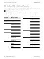
5 SunSpec Modbus Profile - Allocation Tables
5.1
Information on the Allocation Tables
The following sub-sections are sorted in the order of the SunSpec PlugFest Protocol Implementation
Conformance Statement (PICS). Unsupported PICS tables are not listed. The tables are divided into
the sections "Header" and "Fixed Block", in accordance with the PICS. In addition, "Repeating
Block" can be listed. In the tables you will only find the Modbus addresses that must be implemented and those that are implemented optionally.
The columns of the tables show the following information:
Information
Explanation
No (DEC)
Decimal Modbus address (see also Section 3.4.2 "Modbus Register
Number, Register Width and Data Block", page 13 onwards).
Description/Number
Code(s)
[SunSpec description of the Modbus register][(SunSpec name of the
Modbus register)]{<, (SMA: SMA parameter designation>}{<: Parameter>}{<: Number code(s)) = Designation(s)> <(SMA: SMA Number
code designation)>}
The following description scheme is also used in the table sections
"Fixed Block" and "Repeating Block":
• [SunSpec description of the Modbus register] [(SunSpec name of
SunSpec scale factor
the Modbus register)], <Unit><*10
(Register address of the scale factor)>, <(SMA: SMA parameter designation>
For scale factors:
• [Description of the scale factor (SunSpec scale factor): (integer)]
Legend: […] Mandatory entry, <…> Optional entry,
{…} Parameter group
CNT (WORD)
Number of combined Modbus registers at this Modbus address (No).
Type
Data type, e.g. uint32 = 32 bits without prefix (see Section 3.6, page
14).
Access
Access type:
RO: Read only (only Modbus TCP)
RW: Read and write (only Modbus TCP). All RW registers are only
writeable under Modbus UDP (WO registers).
WO: Write only
If an access type is not allowed, a Modbus exception is generated in
the event of access with an access type that is not allowed.
Technical Description
SunSpec_Modbus-TB-US-en-14
17
SunSpec Modbus Profile - Allocation Tables
SMA America, LLC
Damage to SMA inverters
The parameters of the SMA inverters that can be changed with writable Modbus registers
(RW/WO) are intended for long-term storage of device settings. Cyclical changing of these parameters leads to destruction of the flash memory of the devices.
•
Device parameters must not be changed cyclically.
Parameters for the control and limitation of the nominal PV system power - identified in this document with the appendix Parameter for PV system control - are an exception. Such parameters
can be changed cyclically.
Offset of Modbus register number (No)
To read or to write Modbus registers in each case use register numbers reduced by the
offset of 1. Example: Modbus register address = Modbus register number in SunSpec
Modbus profile – offset = 40001 - 1 = 40000.
Device-dependent availability of the Modbus registers
Depending on the SMA device type used, only certain Modbus registers are available. You
will find a table of Modbus registers supported by each inverter type in the technical
information SunSpec Modbus Interface at www.SMA-Solar.com
Value range of cos φ
The value range of cos φ depends on the device. The value range that can be set via the
Modbus protocol cannot be converted by every inverter to physical values (displacement
power factor cos φ, see the operating manual of the inverter).
Reactive power in SunSpec Modbus Profile
For all of the Modbus registers in this document which reactive power is measured or
specified with the following has to be considered: According to IEC convention and to a
four-quadrant generator system a positive reactive power is “inductive“ and a negative
reactive power is “capacitive”.
This is valid for the following Modbus registers: 40206, 40274 and 40359.
18
SunSpec_Modbus-TB-US-en-14
Technical Description
SMA America, LLC
Description/Number Code(s)
Access
Table C 001 (Common Model)
Type
5.2.1
CNT
(WORD)
SunSpec (PICS) - Allocation Tables
No
(DEC)
5.2
SunSpec Modbus Profile - Allocation Tables
2
uint32
RO
1
uint16
RO
1
uint16
RO
Header:
40001
40003
40004
SunSpec ID (SID):
0x53756e53 = SunSpec Modbus Map
Model ID (ID):
1 = SunSpec Common Model
Number of the following Modbus registers in accordance with
the PICS table (L): 66
Fixed Block:
40005
Manufacturer (Mn):
"SMA"
16
string
RO
40021
Model (Md):
„"Solar Inverter"
16
string
RO
8
string
RO
8
string
RO
16
string
RO
Options (Opt), (SMA: Device type):
40037 Numerical identification of the SMA device type (Breakdown
see technical information SunSpec Modbus Interface)
40045
Version (Vr), (SMA: Firmware number):
see Section 3.7 "SMA Firmware Data Format", page 15
40053 Serial number (SN)
Technical Description
SunSpec_Modbus-TB-US-en-14
19
SMA America, LLC
Access
Description/Number code
Type
Table NC 011 (Ethernet Link Layer Model)
CNT
(WORD)
5.2.2
No
(DEC)
SunSpec Modbus Profile - Allocation Tables
40071
Model ID (ID):
11 = SunSpec Ethernet link layer model
1
uint16
RO
40072
Number of the following Modbus registers in accordance with
the PICS table (L): 13
1
uint16
RO
Ethernet data transfer rate (Spd),
(SMA: Data transfer rate of network terminal A):
40073
10 = 10 Mbit/s
100 = 100 Mbit/s
1
uint16
RO
Interface status (CfgSt),
40074 (SMA: Duplex mode of network terminal A):
Bit 1 = Full duplex
1
bitfield
16
RO
Connection status (St), (SMA: Speedwire connection status of
network terminal A):
40075
1 = Activated
2 = Deactivated
1
enum
16
RO
40076 MAC address (MAC)
4
uint64
RO
Header:
Access
Description/Number code
Type
Table NC 012 (IPv4 Model)
CNT
(WORD)
5.2.3
No
(DEC)
Fixed Block:
40086
Model ID (ID):
12 = SunSpec IPv4 Model
1
uint16
RO
40087
Number of the following Modbus registers in accordance with
the PICS table (L): 98
1
uint16
RO
Header:
20
SunSpec_Modbus-TB-US-en-14
Technical Description
SMA America, LLC
SunSpec Modbus Profile - Allocation Tables
Fixed Block:
40092
40093
40094
40095
Configuration status (CfgSt):
1 = valid setting (current setting is valid)
Change status (ChgSt):
Bit 0 = pending change
Change capability (Cap):
Bit 5 = hardware configuration possible
IPv4 Configuration (Cfg), (SMA: Automatic Speedwire configuration switched on):
0 = manual configuration (see information "Network Configuration")
1
enum
16
RO
1
bitfield
16
RO
1
bitfield
16
RO
1
enum
16
RW
1
enum
16
RO
1 = Use DHCP
40096
Configure service use (Ctl):
0 = Activate DNS
40097
IP address (Addr), (SMA: Speedwire IP address):
XXX.XXX.XXX.XXX (see information „Network Configuration“, below)
8
string
RW
40105
Net mask (Msk), (SMA: Speedwire subnet mask): XXX.XXX.XXX.XXX (see
information "Network Configuration", below)
8
string
RW
40113
Gateway (Gw), (SMA: Speedwire gateway address): XXX.XXX.XXX.XXX
(see information „Network Configuration“, below)
8
string
RW
8
string
RW
DNS 1 (DNS1), (SMA: Speedwire DNS server address):
40121 XXX.XXX.XXX.XXX (see information „Network Configuration“,
below)
Network Configuration
A change to the network configuration will only be adopted by the SMA device if each of
the registers 40095, 40097, 40105, 40113 and 40121 are changed. If, for example,
you change the IPv4 configuration (Cfg) with the register 40095 to the value 0 (manual
configuration) and would like to change the IP address with the register 40097, you must
change the other three registers within 60 seconds, or reset them to the same values.
Technical Description
SunSpec_Modbus-TB-US-en-14
21
SMA America, LLC
SunSpec Modbus Profile - Allocation Tables
5.2.4
Tables I 101, 102, 103 (Inverter Integer Map)
Type
Access
1
uint16
RO
1
uint16
RO
40188 AC current (A), in A*10A_SF (40192).
1
uint16
RO
40189 Current, line conductor L1 (AphA), in A*10A_SF (40192).
1
uint16
RO
40190 Current, line conductor L2 (AphB), in A*10A_SF (40192).
1
uint16
RO
40191 Current, line conductor L3 (AphC), in A*10A_SF (40192).
1
uint16
RO
40192 Scale factor current (A_SF): -1
1
sunssf
RO
1
uint16
RO
1
uint16
RO
1
uint16
RO
1
uint16
RO
1
uint16
RO
No
(DEC)
CNT
(WORD)
The following table is valid for each of the three connection models (Model ID). If, for example, the
connection model "Delta connection" is present, table I 102 with the ID = 102 is valid.
Description/Number code
Header:
Model ID (ID):
40186
101 = SunSpec Inverter Model (phsA, phsB, phsC)
102 = SunSpec Inverter Model (phsAB, phsAC, phsBC)
103 = SunSpec Inverter Model (phsABC)
40187
Number of the following Modbus registers in accordance with
the PICS table (L): 50
Fixed Block:
V_SF
40193
Voltage, line conductor L1 to L2 (PPVphAB), in V*10
(40199).
40194
Voltage, line conductor L2 to L3 (PPVphBC), in V*10
(40199).
40195
Voltage, line conductor L3 to L1 (PPVphCA), in V*10
(40199).
40196
Voltage, line conductor L1 to N (PhVphA), in V*10
(40199).
40197
Voltage, line conductor L2 to N (PhVphB), in V*10
(40199).
22
V_SF
V_SF
V_SF
SunSpec_Modbus-TB-US-en-14
V_SF
Technical Description
SMA America, LLC
40198
SunSpec Modbus Profile - Allocation Tables
V_SF
Voltage, line conductor L3 to N (PhVphC), in V*10
(40199).
1
uint16
RO
1
sunssf
RO
1
int16
RO
1
sunssf
RO
1
uint16
RO
1
sunssf
RO
1
int16
RO
1
sunssf
RO
1
int16
RO
1
sunssf
RO
1
int16
RO
1
sunssf
RO
1
acc32
RO
2
sunssf
RO
1
int16
RO
40218 Scale factor DC power (DCW_SF): 2
1
sunssf
RO
40219 Internal temperature (TmpCab), in °C
1
int16
RO
1
int16
RO
40223 Scale factor temperature (Tmp_SF): 0
1
sunssf
RO
Operating status (St):
1 = Off
2 = Wait for PV voltage
3 = Starting
40224 4 = MPP
5 = Regulated
6 = Shutting down
7 = Error
8 = Waiting for electric utility company
1
enum
16
RO
40199 Scale factor voltage (V_SF): -1
W_SF
40200 Active power (W), in W*10
(40201).
40201 Scale factor active power (W_SF): 1
Hz_SF
40202 Power frequency (Hz), in Hz*10
(40203).
40203 Scale factor power frequency (Hz_SF): -2
VA_SF
40204 Apparent power (VA), in VA*10
(40205).
40205 Scale factor apparent power (VA_SF): 1
VAr_SF
40206 Reactive power (VAr), in var*10
(40207).
40207 Scale factor reactive power (VAr_SF): 1
PF_SF
40208 Displacement power factor cos φ (PF)*10
(40209).
40209 Scale factor displacement power factor (PF_SF): -3
WH_SF
40210 Total yield (WH), in Wh*10
(40212).
40212 Scale factor total yield (WH_SF): 1
DCW_SF
40217 DC power (DCW), in W*10
40222
(40218).
Tmp_SF
Other Temperature (TmpOt), in °C*10
External temperature).
Technical Description
(40223), (SMA:
SunSpec_Modbus-TB-US-en-14
23
SMA America, LLC
SunSpec Modbus Profile - Allocation Tables
Event number (Evt1):
Bit 0 = Grounding error / insulation error
Bit 1 = DC overvoltage
Bit 5 = Grid disconnected
Bit 6 = Enclosure open
Bit 7 = Shut down manually
Bit 8 = Overtemperature
40226 Bit 9 = Overfrequency
2
Bit 10 = Underfrequency
bitfield
32
RO
Bit 11 = AC overvoltage
Bit 12 = AC undervoltage
Bit 13 = String fuse defective
Bit 14 = Undertemperature
Bit 15 = Storage or communication error
Access
Description/Number code
Type
Table IC 120 (Inverter Controls Nameplate Ratings)
CNT
(WORD)
5.2.5
No
(DEC)
Bit 16 = Error during hardware test
1
uint16
RO
1
uint16
RO
1
enum
16
RO
1
uint16
RO
1
sunssf
RO
Header:
40238
40239
Model ID (ID):
120 = SunSpec Nameplate Model
Number of the following Modbus registers in accordance with
the PICS table (L): 26
Fixed Block:
40240
40241
DER type (DERTyp), (SMA: Device type):
4 = PV device
WRtg_SF
Continuous active power capability (WRtg), in W*10
(40242), (SMA: Maximum device active power).
40242 Scale factor continuous active power capability (WRtg_SF): 2
24
SunSpec_Modbus-TB-US-en-14
Technical Description
SMA America, LLC
SunSpec Modbus Profile - Allocation Tables
Continuous apparent power capability (VARtg)
VARtg_SF
40243 in VA*10
(40244), (SMA: Maximum device apparent
power).
1
uint16
RO
1
sunssf
RO
Continuous reactive power capability in quadrant 1
VArRtg_SF
40245 (VArRtgQ1), in VAr*10
(40249), (SMA: Maximum
device reactive power in quadrant 1).
1
int16
RO
Continuous reactive power capability in quadrant 2
VArRtg_SF
40246 (VArRtgQ2), in VAr*10
(40249), (SMA: Maximum
device reactive power in quadrant 2).
1
int16
RO
Continuous reactive power capability in quadrant 3
VArRtg_SF
40247 (VArRtgQ3), in VAr*10
(40249), (SMA: Maximum
device reactive power in quadrant 3).
1
int16
RO
Continuous reactive power capability in quadrant 4
VArRtg_SF
40248 (VArRtgQ4), in VAr*10
(40249), (SMA: Maximum
device reactive power in quadrant 4).
1
int16
RO
1
sunssf
RO
40244
Scale factor continuous apparent power capability (VARtg_SF):
2
40249
Scale factor continuous reactive power capability (VArRtg_SF):
2
40250
Continuous RMS current capability (ARtg), in A*10
(40251), (SMA: nominal current across all line conductors).
1
uint16
RO
40251 Scale factor continuous RMS current capability (Artg_Rtg): 0
1
sunssf
RO
Minimum displacement power factor capability in Q 1
PFRtg_SF
40252 ((PFRtgQ1)*10
(40256), (SMA: Minimum displacement
power factor cos φ in Q 1).
1
int16
RO
Minimum displacement power factor capability in Q 2
PFRtg_SF
40253 ((PFRtgQ2)*10
(40256), (SMA: Minimum displacement
power factor cos φ in Q 2).
1
int16
RO
Minimum displacement power factor capability in Q 3
PFRtg_SF
40254 ((PFRtgQ3)*10
(40256), (SMA: Minimum displacement
power factor cos φ in Q 3).
1
int16
RO
Technical Description
ARtg_SF
SunSpec_Modbus-TB-US-en-14
25
SMA America, LLC
SunSpec Modbus Profile - Allocation Tables
Minimum displacement power factor capability in Q 4
PFRtg_SF
40255 ((PFRtgQ4)*10
(40256), (SMA: Minimum displacement
power factor cos φ in Q 4).
1
sunssf
RO
Nominal capacity of the storage device (WHRtg),
WHRtg_SF
40257 in Wh*10
(40258), (SMA: Nominal capacity of the
battery).
1
uint16
RO
40258 Scale factor nominal capacity (WHRtg_SF): 2
1
sunssf
RO
1
uint16
RO
40260 Scale factor usable Ah capacity (AhrRtg_SF): 0
1
sunssf
RO
Maximum energy transfer rate to the storage device
MaxChaRte_SF
40261 (MaxChaRte), in W*10
(40262), (SMA: Maximum
charging power of the battery).
1
uint16
RO
Scale factor maximum energy transfer rate to the storage device
(MaxChaRte_SF): 2
1
sunssf
RO
1
uint16
RO
1
sunssf
RO
40256
40259
40262
Scale factor minimum displacement power factor capability
(PFRtg_SF): -1
AhrRtg_SF
Usable Ah capacity of the battery (AhrRtg), in Ah*10
(40260), (SMA: Usable nominal capacity of the battery).
40264
Scale factor maximum energy transfer rate from the storage
device (MaxDisChaRte_SF): 2
5.2.6
Table IC 121 (Inverter Controls Basic Settings)
No
(DEC)
Maximum energy transfer rate from the storage device
MaxDisChaRte_SF
40263 (MaxDisChaRte), in W*10
(40264), (SMA:
Maximum discharging power of the battery).
Description/Number code
Access
RO
Type
int16
CNT
(WORD)
1
1
uint16
RO
1
uint16
RO
Header:
40266
40267
26
Model ID (ID):
121 = SunSpec Basic Settings Model
Number of the following Modbus registers in accordance with
the PICS table (L): 30
SunSpec_Modbus-TB-US-en-14
Technical Description
SMA America, LLC
SunSpec Modbus Profile - Allocation Tables
Fixed Block:
40268
Setting for maximum output active power (WMax),
WMax_SF
in W*10
(40288), (SMA: Set active power limit).
40269
Voltage at the PCC (VRef), in V*10
(40289), (SMA:
Reference voltage for the system control).
VRef_SF
1
uint16
RW
1
uint16
RW
1
int16
RW
VRefOfs_SF
Offset between PCC and inverter (VRefOfs), in V*10
40270 (40290), (SMA: Reference correction voltage for the system
control).
40273
Set value for maximum apparent power (VAMax),
VAMax_SF
in VA*10
(40292), (SMA: Set apparent power limit).
1
uint16
RW
40274
Maximum reactive power in Q 1 (VArMaxQ1),
VArMax_SF
in var*10
(40293), (SMA: Set reactive power limit).
1
int16
RW
Standard active power increase rate (WGra), in % of
WGra_SF
40278 (WMax/min)*10
(40294), (SMA: active power gradient).
1
uint16
RW
VAr action when changing between charging and discharging
(VArAct), (SMA: Reaction of the excitation when changing the
40283 direction of power flow):
1 = Change excitation type
2 = Do not change excitation type
1
enum
16
RW
1
uint16
RW
Identity of the line conductor in single-phase inverters (ConnPh),
(SMA: Line conductor assignment):
40287 1 = Line conductor L1
2 = Line conductor L2
3 = Line conductor L3
1
enum
16
RW
40288 Scale factor for output active power (WMax_SF): 2
1
sunssf
RO
40289 Scale factor reference current (VRef_SF): 0
1
sunssf
RO
40290 Scale factor for offset (VRefOfs_SF): 0
1
sunssf
RO
40292 Scale factor for apparent power (VAMax_SF): 2
1
sunssf
RO
40293 Scale factor for reactive power (VArMax_SF): 2
1
sunssf
RO
40294 Scale factor active power increase rate (WGra_SF): 0
1
sunssf
RO
40297 Scale factor nominal frequency (ECPNomHz_SF): 0
1
sunssf
RO
40286
Set value for nominal frequency (ECPNomHz),
ECPNomHz_SF
in Hz*10
(40297), (SMA: Nominal frequency).
Technical Description
SunSpec_Modbus-TB-US-en-14
27
SMA America, LLC
Access
Description/Number code
Type
Table IC 122 (Inverter Controls Extended Measurements)
CNT
(WORD)
5.2.7
No
(DEC)
SunSpec Modbus Profile - Allocation Tables
1
uint16
RO
1
uint16
RO
1
bitfield
16
RO
1
bitfield
16
RO
ECP connection status (ECPConn), (SMA: PV system utility grid
40302 connection):
Bit 0 = Connected
1
bitfield
16
RO
40303 Total active power yield (ActWh), in Wh, (SMA: Total yield).
4
acc64
RO
1
uint16
RO
1
sunssf
RO
Header:
40298
40299
Model ID (ID):
122 = SunSpec Measurements Status Model
Number of the following Modbus registers in accordance with
the PICS table (L): 44
Fixed Block:
PV inverter availability status (PVConn), (SMA: Status of the grid
relay):
40300 Bit 0 = Connected
Bit 1 = Available
Bit 2 = In operation
Battery inverter availability status (StorConn), (SMA: Status of
the battery):
40301 Bit 0 = Connected
Bit 1 = Available
Bit 2 = In operation
Ris_SF
40342 Insulation resistance (Ris), in Ω*10
(40343).
40343 Scale factor insulation resistance (Ris_SF): 4
28
SunSpec_Modbus-TB-US-en-14
Technical Description
SMA America, LLC
Access
Description/Number code
Type
Table IC 123 (Immediate Inverter Controls)
CNT
(WORD)
5.2.8
No
(DEC)
SunSpec Modbus Profile - Allocation Tables
1
uint16
RO
1
uint16
RO
1
enum
16
WO
1
uint16
WO
1
enum
16
RW
1
int16
WO
1
enum
16
RW
1
int16
WO
Header:
40344
40345
Model ID (ID):
123 = SunSpec Immediate Controls Model
Number of the following Modbus registers in accordance with
the PICS table (L): 24
Fixed Block:
Parameter for PV system control :
40348
Connection control (Conn), (SMA: Quick disconnect):
0 = Not connected
1 = Connected
Parameter for PV system control :
40349
Set power to default value ((WMaxLimPct), in % of
WMaxLimPct_SF
WMax*10
(40367), (SMA: Normalized active
power limitation via the system control).
Choking (WMaxLim_Ena), (SMA: Operating mode of the feed40353 in management):
1 = Activated
Parameter for PV system control :
40354
OutPFSet_SF
Set power factor to a certain value (OutPFSet)*10
(40368), (SMA: specification of the displacement power factor
cos φ via the system control).
Fixed power factor (OutPFSet_Ena), (SMA: operating mode of
40358 the static voltage stability):
1 = Activated
Parameter for PV system control :
40359
VArPct_SF
Reactive power (VArWMaxPct), in % of WMax*10
(40369), (SMA: Normalized reactive power limitation via the
system control).
Technical Description
SunSpec_Modbus-TB-US-en-14
29
SMA America, LLC
SunSpec Modbus Profile - Allocation Tables
Mode of the percentile reactive power limitation (VArPct_Mod):
1
enum
16
RO
Control of the reactive power limitation (VArPct_Ena), (SMA:
40366 Operating mode of the static voltage stability):
1 = Activated
1
enum
16
RW
40367 Scale factor power specification value (WMaxLimPct_SF): 0
1
sunssf
RO
40368 Scale factor power factor (OutPFSet_SF): -4
1
sunssf
RO
40369 Scale factor reactive power (VArPct_SF): -1
1
sunssf
RO
1 = in % of WMax
Access
Description/Number code
Type
Table IC 124 (Basic Storage Controls)
CNT
(WORD)
5.2.9
No
(DEC)
40365
1
uint16
RO
1
uint16
RO
Set value for maximum charging active power (WChaMax),
ChaMax_SF
in W*10W
(40388). Reference value for WChaGra
40372
and WDisChaGra, (SMA maximum charging power of the
battery manufacturer).
1
uint16
RW
Activation of the storage control mode (StorCtl_Mod), (SMA:
operating mode of the battery management system):
40375
Bit 0 = Battery charging
Bit 1 = Battery discharging
1
bitfield
16
RW
Current available energy (ChaState), in % of
ChaState_SF
40378 AhrRtg*10
(40392), (SMA: Current battery state of
charge).
1
uint16
RO
1
uint16
RO
Header:
40370
40371
Model ID (ID):
124 = SunSpec Storage Model
Number of the following Modbus registers in accordance with
the PICS table (L): 24
Fixed Block:
40380
30
InBatV_SF
Battery internal voltage (InBatV), in V*10
(SMA: Battery voltage).
SunSpec_Modbus-TB-US-en-14
(40394),
Technical Description
SMA America, LLC
SunSpec Modbus Profile - Allocation Tables
State of charge of the storage device (ChaSt), (SMA: Operating status of battery):
1 = Off
40381
3 = Discharging
4 = Charging
6 = Float charge
1
enum
16
RO
40388 Scale factor charging active power (WChaMax_SF): 0
1
sunssf
RO
40392 Scale factor available energy (ChaState_SF): 0
1
sunssf
RO
40394 Scale factor battery-internal voltage (InBatV_SF): -2
1
sunssf
RO
Type
Access
1
uint16
RO
1
uint16
RO
40398 0 = No curve active (deactivated)
1
uint16
RW
Volt-VAR control active (ModEna), (SMA: operating mode of
40399 the static voltage stability):
Bit 0 = Activated
1
bitfield
16
RW
40403 Number of supported curves (NCrv): 1
1
uint16
RO
40404 Number of supported curve points (NPt): 12
1
uint16
RO
40405 Scale factor voltage points (V_SF): -2
1
sunssf
RO
40406 Scale factor reference variables (DeptRef_SF): 2
1
sunssf
RO
40407 Scale factor ramp (RmpIncDec_SF): 0
1
sunssf
RO
No
(DEC)
CNT
(WORD)
5.2.10 Table IC 126 (Static Volt-VAR Arrays)
Description/Number code
Header:
40396
40397
Model ID (ID):
126 = SunSpec Static Volt-VAR Model
Number of the following Modbus registers in accordance with
the PICS table (L): 64
Fixed Block:
Index of the active curve (ActCrv):
1 = Curve 1 active
Technical Description
SunSpec_Modbus-TB-US-en-14
31
SMA America, LLC
SunSpec Modbus Profile - Allocation Tables
Repeating Block (see number of supported curves (40403)):
Static volt-VAR curve definition.
40408
Number of active points in the array (ActPt), (SMA: Characteristic curve, number of points for use on the characteristic curve)
40409
Assigning of the reference variables (DeptRef)*10
(40406): 1 = WMax
40410
Point 1 volt (V1), in % of VRef*10
1 of characteristic curve 1).
40411
Point 1 VAr (VAr1)*10
characteristic curve 1).
40412
Point 2 volts (V2), in % of VRef*10
2 of characteristic curve 1).
40413
Point 2 VAr (VAr2)*10
characteristic curve 1).
40414
Point 3 volts (V3), in % of VRef*10
3 of characteristic curve 1).
40415
Point 3 VAr (VAr3)*10
characteristic curve 1).
40416
Point 4 volts (V4), in % of VRef*10
4 of characteristic curve 1).
40417
Point 4 VAr (VAr4)*10
characteristic curve 1).
40418
Point 5 volts (V5), in % of VRef*10
5 of characteristic curve 1).
40419
Point 5 VAr (VAr5)*10
characteristic curve 1).
40420
Point 6 volts (V6), in % of VRef*10
6 of characteristic curve 1).
40421
Point 6 VAr (VAr6)*10
characteristic curve 1).
40422
Point 7 volts (V7), in % of VRef*10
7 of characteristic curve 1).
32
DeptRef_SF
V_SF
DeptRef_SF
(40405), (SMA: X value
(40406), (SMA: Y value 1 of
V_SF
DeptRef_SF
(40406), (SMA: Y value 2 of
V_SF
DeptRef_SF
SunSpec_Modbus-TB-US-en-14
(40405), (SMA: X value
(40406), (SMA: Y value 5 of
V_SF
DeptRef_SF
(40405), (SMA: X value
(40406), (SMA: Y value 4 of
V_SF
DeptRef_SF
(40405), (SMA: X value
(40406), (SMA: Y value 3 of
V_SF
DeptRef_SF
(40405), (SMA: X value
(40405), (SMA: X value
(40406), (SMA: Y value 6 of
V_SF
(40405), (SMA: X value
1
uint16
RW
1
enum
16
RO
1
uint16
RW
1
int16
RW
1
uint16
RW
1
int16
RW
1
uint16
RW
1
int16
RW
1
uint16
RW
1
int16
RW
1
uint16
RW
1
int16
RW
1
uint16
RW
1
int16
RW
1
uint16
RW
Technical Description
SMA America, LLC
SunSpec Modbus Profile - Allocation Tables
DeptRef_SF
40423
Point 7 VAr (VAr7)*10
characteristic curve 1).
(40406), (SMA: Y value 7 of
40424
Point 8 volts (V8), in % of VRef*10
8 of characteristic curve 1).
40425
Point 8 VAr (VAr8)*10
characteristic curve 1).
40426
Point 9 volts (V9), in % of VRef*10
9 of characteristic curve 1).
40427
Point 9 VAr (VAr9)*10
characteristic curve 1).
40428
Point 10 volts (V10), in % of VRef*10
value 10 of characteristic curve 1).
40429
Point 10 VAr (VAr10)*10
of characteristic curve 1).
40430
Point 11 volts (V11), in % of VRef*10
value 11 of characteristic curve 1).
40431
Point 11 VAr (VAr11)*10
of characteristic curve 1).
40432
Point 12 volts (V12), in % of VRef*10
value 12 of characteristic curve 1).
40433
Point 12 VAr (VAr12)*10
of characteristic curve 1).
1
int16
RW
1
uint16
RW
1
int16
RW
1
uint16
RW
1
int16
RW
1
uint16
RW
1
int16
RW
1
uint16
RW
1
int16
RW
1
uint16
RW
1
int16
RW
The maximum rate at which the VAr value is decreased depending on voltage changes (RmpDecTmm), in % of DeptRef
40459
RmpIncDec_SF
(40409)*10
(40407), (SMA: Decrease ramp for
achieving the characteristic curve operating point).
1
uint16
RW
The maximum rate at which the VAr value is increased depending on voltage changes (RmpIncTmm), in % of DeptRef
40460
RmpIncDec_SF
(40409)*10
(40407), (SMA: Increase ramp for
achieving the characteristic curve operating point).
1
uint16
RW
Boolean flag, which indicates whether the curve points can be
40461 changed or not (ReadOnly):
0 = Activated
1
enum
16
RO
V_SF
DeptRef_SF
(40406), (SMA: Y value 8 of
V_SF
DeptRef_SF
(40405), (SMA: X value
(40405), (SMA: X value
(40406), (SMA: Y value 9 of
V_SF
DeptRef_SF
(40406), (SMA: Y value 10
V_SF
DeptRef_SF
Technical Description
(40405), (SMA: X
(40406), (SMA: Y value 11
V_SF
DeptRef_SF
(40405), (SMA: X
(40405), (SMA: X
(40406), (SMA: Y value 12
SunSpec_Modbus-TB-US-en-14
33
SMA America, LLC
SunSpec Modbus Profile - Allocation Tables
Type
Access
1
uint16
RO
1
uint16
RO
Gradient of the reduction of the maximum active power as a
WGra_SF
function of the frequency (WGra), in % of PM/Hz*10
40464
(40470), (SMA: Active power gradient, configuration of the
linear gradients of the current power).
1
uint16
RW
Frequency deviation from the nominal frequency (ECPNomHz),
at which the current power is used as limiting value for the
40465 output power (HzStr), in Hz*10HzStrStop_SF (40471), (SMA:
Distance of the start frequency from the power frequency,
configuration of the linear gradients of the current power).
1
int16
RW
Frequency deviation from the nominal frequency (ECPNomHz),
at which the limited current power returns to the normal value
HzStrStop_SF
and the limiting is removed (HzStop), in Hz*10
40466
(40471), (SMA: Distance of the reset frequency from the power
frequency, configuration of the linear gradients of the current
power).
1
int16
RW
Activation of the hysteresis (HysEna), (SMA: Activation of the
stay-set indicator function, configuration of the linear gradients
40467 of the current power):
1
bitfield
16
RW
Configured frequency-power control (ModEna), (SMA: Operating mode of the active power reduction with overfrequency
40468 P(f)):
1
bitfield
16
RW
No
(DEC)
CNT
(WORD)
5.2.11 Table IC 127 (Parameterized Frequency-Watt)
Description/Number code
Header:
40462
40463
Model ID (ID):
127 = SunSpec Frequency-Watt Parameter Model
Number of the following Modbus registers in accordance with
the PICS table (L): 10
Fixed Block:
Bit 0 = Activated
Bit 0 = Activated
34
SunSpec_Modbus-TB-US-en-14
Technical Description
SMA America, LLC
SunSpec Modbus Profile - Allocation Tables
Maximum rate of change at which an output power limited
through overfrequency returns to normal power (HzStopWGra),
40469 in % of WMax/min*10RmpIncDec_SF (40472), (SMA: Active
power gradient after reset frequency, configuration of the linear
gradients of the current power (P-HzStopWGra).
1
uint16
RW
40470 Scale factor gradient (WGra_SF): 0
1
sunssf
RO
40471 Scale factor frequency deviation (HzStrStop_SF): -2
1
sunssf
RO
40472 Scale factor ramp (RmpIncDec_SF): 0
1
sunssf
RO
Type
Access
1
uint16
RO
1
uint16
RO
1
enum
16
RW
Gradient for the increase in leading, dynamic current (ArArGra_SF
GraSag), in % of ARtg/dV*10
(40487), (SMA: Gradi40477
ent K of the reactive current droop for undervoltage with dynamic grid support).
1
uint16
RW
Gradient for the increase in lagging, dynamic current (ArGraSArGra_SF
well), in % of ARtg/dV*10
(40487), (SMA: Gradient K
40478
of the reactive current droop for overvoltage with dynamic grid
support).
1
uint16
RW
No
(DEC)
CNT
(WORD)
5.2.12 Table IC 128 (Dynamic Reactive Current)
Description/Number code
Header:
40474
40475
Model ID (ID):
128 = SunSpec Dynamic Reactive Current Model
Number of the following Modbus registers in accordance with
the PICS table (L): 14
Fixed Block:
Indicates whether a gradient it to run on the edge or in the
center of the deadband against zero (ArGraMod), (SMA:
Reactive current droop, configuration of the full dynamic grid
40476 support):
0 = Edge
1 = Center
Technical Description
SunSpec_Modbus-TB-US-en-14
35
SMA America, LLC
SunSpec Modbus Profile - Allocation Tables
Activates the dynamic reactive voltage model (ModEna), (SMA:
Operating mode of the dynamic grid support, configuration of
40479 the dynamic grid support):
1
bitfield
16
RW
1
uint16
RO
Lower voltage deadband, below which voltage changes do not
cause changes to the dynamic grid support (DbVMin), in % of
40481
VRefPct_SF
VRef*10
(40488), (SMA: Lower limit voltage deadband, configuration of the full dynamic grid support).
1
uint16
RW
Upper voltage deadband, above which voltage changes do not
cause changes to the dynamic grid support (DbVMax), in % of
40482
VRefPct_SF
VRef*10
(40488), (SMA: Upper limit voltage deadband, configuration of the full dynamic grid support).
1
uint16
RW
Voltage of the block zone, below which no dynamic current will
VRefPct_SF
be produced (BlkZnV), in % of VRef*10
(40488),
40483
(SMA: PWM cut-off voltage, configuration of the dynamic grid
support).
1
uint16
RW
Time period of the block zone, within which no changes to the
-3
40485 dynamic current occur (BlkZnTmms), in s*10 , (SMA: PWM
cut-off delay, configuration of the dynamic grid support).
1
uint16
RW
40487 Scale factor gradient (ArGra_SF): -2
1
sunssf
RO
40488 Scale factor block zone (VRefPct_SF): 0
1
sunssf
RO
Bit 0 = Activated
40480
Time period for the calculation of the sliding voltage average
(FilTms), in s: 60
Type
Access
Description/Number code
CNT
(WORD)
No
(DEC)
5.2.13 Table IC 131 (Watt-Power Factor)
1
uint16
RO
1
uint16
RO
Header:
40490
40491
36
Model ID (ID):
131 = SunSpec Watt-PF Model
Number of the following Modbus registers in accordance with
the PICS table (L): 64
SunSpec_Modbus-TB-US-en-14
Technical Description
SMA America, LLC
SunSpec Modbus Profile - Allocation Tables
Fixed Block:
Index of the active curve (ActCrv):
40492 0 = No curve active (deactivated)
1
uint16
RW
Watt-PF mode active (ModEna), (SMA: operating mode of the
40493 static voltage stability):
Bit 0 = Activated
1
bitfield
16
RW
40498 Number of supported curve points (NPt): 2
1
uint16
RO
40499 Scale factor power points (W_SF): 0
1
sunssf
RO
40500 Scale factor cos φ points (PF_SF): -2
1
sunssf
RO
1
uint16
RO
1
int16
RW
1
int16
RW
1
int16
RW
Point 2 PF in EEI notation (PF2), cos φ*10
(40500), (SMA:
40506 cos φ of the end point, configuration of the cos φ (P) characteristic curve).
1
int16
RW
Boolean flag, which indicates whether the curve points can be
40554 changed or not (ReadOnly):
0 = Activated
1
enum
16
RO
1 = Curve 1 active
Repeating Block: Watt-PF curve definition.
40502 Number of active points in the array (ActPt): 2
W_SF
Point 1 watt (W1), in % of WMax*10
(40499), (SMA:
40503 Active power of the start point, configuration of the cos φ(P)
characteristic curve).
PF_SF
Point 1 PF in EEI notation (PF1), cos φ*10
(40500), (SMA:
40504 cos φ of the start point, configuration of the cos φ (P) characteristic curve).
W_SF
Point 2 watts (W2), in % of WMax*10
(40499), (SMA:
40505 Active power of the end point, configuration of the cos φ(P)
characteristic curve).
PF_SF
Technical Description
SunSpec_Modbus-TB-US-en-14
37
SMA America, LLC
SunSpec Modbus Profile - Allocation Tables
Type
Access
1
uint16
RO
1
uint16
RO
Index of the active curve (ActCrv): (SMA: Characteristic curve
number): 1 = Curve 1 active
1
uint16
RW
Volt-watt control active (ModEna), (SMA: Configuration of the
40559 active power/voltage characteristic curve P(V)):
Bit 0 = Activated
1
bitfield
16
RW
40563 Number of supported curves (NCrv): 1
1
uint16
RO
40564 Number of supported curve points (NPt): 12
1
uint16
RO
40565 Scale factor voltage points (V_SF): -2
1
sunssf
RO
40566 Scale factor reference variables (DeptRef_SF): -2
1
sunssf
RO
No
(DEC)
CNT
(WORD)
5.2.14 Table IC 132 (Volt-Watt)
Description/Number code
Header:
40556
40557
Model ID (ID):
132 = SunSpec Volt-Watt Model
Number of the following Modbus registers in accordance with
the PICS table (L): 64
Fixed Block:
40558
Repeating Block (see number of supported curves (40563)): Volt-watt curve definition.
40568 Number of active points in the array (ActPt)
DeptRef_SF
40569
Assigning of the reference variables (DeptRef)*10
(40566): 1 = in % of WMax
40570
Point 1 volt (V1), in % of VRef*10
1 of characteristic curve 1).
40571
Point 1 watt (W1), in % of DeptRef*10
(SMA: Y value 1 of characteristic curve 1).
40572
Point 2 volts (V2), in % of VRef*10
2 of characteristic curve 1).
38
V_SF
(40565), (SMA: X value
DeptRef_SF
SunSpec_Modbus-TB-US-en-14
V_SF
(40566),
(40565), (SMA: X value
1
uint16
RW
1
enum
16
RO
1
uint16
RW
1
int16
RW
1
uint16
RW
Technical Description
SMA America, LLC
SunSpec Modbus Profile - Allocation Tables
DeptRef_SF
40573
Point 2 watts (W2), in % of DeptRef*10
(SMA: Y value 2 of characteristic curve 1).
40574
Point 3 volts (V3), in % of VRef*10
3 of characteristic curve 1).
40575
Point 3 watts (W3), in % of DeptRef*10
(SMA: Y value 3 of characteristic curve 1).
40576
Point 4 volts (V4), in % of VRef*10
4 of characteristic curve 1).
40577
Point 4 watts (W4), in % of DeptRef*10
(SMA: Y value 4 of characteristic curve 1).
40578
Point 5 volts (V5), in % of VRef*10
5 of characteristic curve 1).
40579
Point 5 watts (W5), in % of DeptRef*10
(SMA: Y value 5 of characteristic curve 1).
40580
Point 6 volts (V6), in % of VRef*10
6 of characteristic curve 1).
40581
Point 6 watts (W6), in % of DeptRef*10
(SMA: Y value 6 of characteristic curve 1).
40582
Point 7 volts (V7), in % of VRef*10
7 of characteristic curve 1).
40583
Point 7 watts (W7), in % of DeptRef*10
(SMA: Y value 7 of characteristic curve 1).
40584
Point 8 volts (V8), in % of VRef*10
8 of characteristic curve 1).
40585
Point 8 watts (W8), in % of DeptRef*10
(SMA: Y value 8 of characteristic curve 1).
40586
Point 9 volts (V9), in % of VRef*10
9 of characteristic curve 1).
40587
Point 9 watts (W9), in % of DeptRef*10
(SMA: Y value 9 of characteristic curve 1).
40588
Point 10 volts (V10), in % of VRef*10
value 10 of characteristic curve 1).
V_SF
(40565), (SMA: X value
DeptRef_SF
V_SF
(40566),
(40565), (SMA: X value
DeptRef_SF
Technical Description
(40566),
(40565), (SMA: X value
DeptRef_SF
V_SF
(40566),
(40565), (SMA: X value
DeptRef_SF
V_SF
(40566),
(40565), (SMA: X value
DeptRef_SF
V_SF
(40566),
(40565), (SMA: X value
DeptRef_SF
V_SF
(40566),
(40565), (SMA: X value
DeptRef_SF
V_SF
(40566),
V_SF
(40566),
(40565), (SMA: X
1
int16
RW
1
uint16
RW
1
int16
RW
1
uint16
RW
1
int16
RW
1
uint16
RW
1
int16
RW
1
uint16
RW
1
int16
RW
1
uint16
RW
1
int16
RW
1
uint16
RW
1
int16
RW
1
uint16
RW
1
int16
RW
1
uint16
RW
SunSpec_Modbus-TB-US-en-14
39
SMA America, LLC
SunSpec Modbus Profile - Allocation Tables
DeptRef_SF
40589
Point 10 watts (W10), in % of DeptRef*10
(SMA: Y value 10 of characteristic curve 1).
40590
Point 11 volts (V11), in % of VRef*10
value 11 of characteristic curve 1).
40591
Point 11 watts (W11), in % of DeptRef*10
(SMA: Y value 11 of characteristic curve 1).
40592
Point 12 volts (V12), in % of VRef*10
value 12 of characteristic curve 1).
40593
Point 12 watts (W12), in % of DeptRef*10
(SMA: Y value 12 of characteristic curve 1).
(40566),
1
int16
RW
1
uint16
RW
1
int16
RW
1
uint16
RW
1
int16
RW
The maximum rate, at which the watt value is decreased depending on voltage changes (RmpDecTmm), in % of DeptRef
40619
(40569), (SMA: Decrease ramp for achieving the characteristic
curve operating point).
1
uint16
RO
The maximum rate, at which the watt value is increased depending on voltage changes (RmpIncTmm), in % of DeptRef
40620
(40569), (SMA: Increase ramp for achieving the characteristic
curve operating point).
1
uint16
RO
Boolean flag, which indicates whether the curve points can be
40621 changed or not (ReadOnly):
0 = Activated
1
enum
16
RO
40
V_SF
(40565), (SMA: X
DeptRef_SF
V_SF
SunSpec_Modbus-TB-US-en-14
(40566),
(40565), (SMA: X
DeptRef_SF
(40566),
Technical Description
SMA America, LLC
SunSpec Modbus Profile - Allocation Tables
Type
Access
1
uint16
RO
1
uint16
RO
40624 Scale factor current (DCA_SF): -1
1
sunssf
RO
40625 Scale factor voltage (DCV_SF): 0
1
sunssf
RO
40626 Scale factor power (DCW_SF): 2
1
sunssf
RO
40630 Number of modules (N): 2
1
uint16
RO
1
uint16
RO
No
(DEC)
CNT
(WORD)
5.2.15 Table I 160 (MPPT Inverter Extension Model)
Description/Number code
Header:
40622
40623
Model ID (ID):
160 = SunSpec Multiple MPPT Inverter Extension Model
Number of the following Modbus registers in accordance with
the PICS table (L): 48
Fixed Block:
Repeating Block (see number of supported modules (40630)):
Multiple MPP Tracking Inverter Extension Model.
40632 ID of the MPP tracker (ID): 1
DCA_SF
(40624).
1
uint16
RO
DCV_SF
(40625).
1
uint16
RO
1
uint16
RO
1
uint16
RO
40641 DC current input 1 (DCA), in A*10
40642 DC voltage input 1 (DCV), in V*10
DCW_SF
40643 DC power input 1 (DCW), in W*10
(40626).
40652 ID of the MPP tracker (ID): 2
DCA_SF
(40624).
1
uint16
RO
DCV_SF
(40625).
1
uint16
RO
1
uint16
RO
40661 DC current input 2 (DCA), in A*10
40662 DC voltage input 2 (DCV), in V*10
DCW_SF
40663 DC power input 2 (DCW), in W*10
Technical Description
(40626).
SunSpec_Modbus-TB-US-en-14
41
SMA America, LLC
SunSpec Modbus Profile - Allocation Tables
5.3
SunSpec (PICS) – Grid Guard Parameters
In the following table you will find an overview of the SunSpec Modbus profile parameters that you
can only change after prior transmission of an SMA Grid Guard code.
SMA Grid Guard code
You will find information on the SMA Grid Guard code in Section 2.5 “SMA Grid Guard
Code”, page 11.
PICS table
Modbus register
NC 011
40076
NC 012
40121
IC 120
40250
IC 121
40269
40469
IC 128
40477
40478
40479
40481
40270
40482
40278
40483
40286
IC 123
40353
40358
IC 126
IC 131
40493
40504
40399
40505
40408
IC 127
40485
40503
40398
40410 to 40432
(in steps of 2)
40476
40506
IC 132
40558
40411 to 40433
(in steps of 2)
40559
40464
40570 to 40592
(in steps of 2)
40465
40466
40467
40568
40571 to 40593
(in steps of 2)
40468
42
SunSpec_Modbus-TB-US-en-14
Technical Description
SMA America, LLC
SunSpec Modbus Profile - Allocation Tables
Format
Access
Description/Number code
Type
No (DEC)
Save the Grid Guard code under the Unit ID = 3 in the register 43090 in each inverter. You will
find a detailed description of the register 43090 in the following table:
U32
FIX0
RW
SMA Grid Guard code:
Reading the register:
0 = Not logged in with the Grid Guard code
43090 1 = Logged in with the Grid Guard code
Writing to the register: Log in and activate the Grid Guard
mode using the SMA Grid Guard code.
Logging out: Write 0 in the register to log out of Grid Guard
mode.
Technical Description
SunSpec_Modbus-TB-US-en-14
43
SMA America, LLC
Troubleshooting
6 Troubleshooting
Problem
Cause and corrective measure
The SMA device with Speedwire interface is not available
for the Modbus client.
The necessary Modbus server in the SMA device with Speedwire
interface may not be enabled.
Corrective measures:
• Ensure that the required Modbus server is enabled (see
Section 4 "Commissioning and Configuration", page 16)
The correct IP address for the SMA device with Speedwire interface may not be set in the Modbus client.
Corrective measures:
• Read off the IP address of the SMA device with Speedwire
interface (see router manual).
• Ensure that the correct IP address for the SMA device with
Speedwire interface is set in the Modbus client (see the
Modbus client manufacturer manual).
The firewall may not be set correctly.
Corrective measures:
• Enable port 502 in the firewall (see firewall manual).
The SMA device with SpeedThe Modbus server of the SMA device may be currently overwire interface does not send a loaded.
reply within the response time Corrective measures:
specified by the Modbus client.
• Extend the response time set in the Modbus client successively by one second respectively.
44
SunSpec_Modbus-TB-US-en-14
Technical Description
SMA America, LLC
Troubleshooting
A NaN value is returned when You may be trying to read from a Modbus register that is not
reading a Modbus register
supported by the inverter.
(see Section 3.6 "SunSpec
Corrective measures:
Data Types and NaN Values",
• Contrast and compare the available measured values for
page 14).
your SMA device with the requested Modbus registers (see
technical information SunSpec Modbus Interface at
www.SMA-Solar.com).
You may be trying to read a Modbus register that is not defined
in the SunSpec Modbus profile.
Corrective measures:
• Remove the requested Modbus address from data processing.
• Install an up-to-date Modbus profile by means of a firmware update.
The NaN value 255 is returned. You may be trying to read a
configuration of a non-existing device.
Corrective measures:
• Set the Unit ID = 126 in the Modbus client for the desired
SMA device with Speedwire interface.
• Check if the configuration to be read is supported by the
device.
You may be trying to read an overflown counter (e.g. energy
counter in Wh). In this case the counter contains a NaN value
according to the counter’s data type.
Corrective measures:
• Try to read a counter in a larger unit (e.g. energy counter
in in kWh).
You may be trying to read a write-only Modbus register.
Corrective measures:
• Read off the access type of the Register to be written to
from the "Access" column of the corresponding allocation
table and correct in the Modbus client.
Technical Description
SunSpec_Modbus-TB-US-en-14
45
SMA America, LLC
Troubleshooting
Modbus exception 1 "Illegal
Function" is reported in the
Modbus client.
You may be trying to write a data block to an address range that
contains read-only registers.
Corrective measures:
• Check if all registers to be written are of access type RW.
You, software or a data logger may try to login to a device
several times with a Grid Guard-Code.
Corrective measures:
• Check that only one person, one software instance or one
data logger exclusively tries to login to a device with a
Grid Guard code.
Modbus exception 2 "Illegal
Data Address" is reported in
the Modbus client.
You may be trying to write to a Modbus register that is not defined in the SunSpec Modbus profile.
Corrective measures:
• In the Modbus client check the Modbus address to be written to for errors.
You may be trying to write or to read a data block, which start
address or which end address does not match to those of a
register (alignment mismatch).
Corrective measures:
• Check the start address or the end address of the data
block.
• Check the registers at the start address or at the end address of the data block for consistency. May be one of
both registers is not consistent.
You may be trying to write a data block and one of the registers
is not supported by the device.
Corrective measures:
• Check if the register to be written to is supported by your
device (see technical information SunSpec Modbus Interface at www.SMA-Solar.com).
46
SunSpec_Modbus-TB-US-en-14
Technical Description
SMA America, LLC
Modbus exception 3 "Illegal
Data Value" is reported in the
Modbus client.
Troubleshooting
You may be trying to write a data block (Modbus commands
0x10 and 0x17) and one of the values has a data type that is
not permitted.
Corrective measures:
• Read off the data type of the register to be written to from
the "Type" column of the corresponding allocation table
and correct in the Modbus client.
Modbus exception 4 “Slave
Device Failure” is reported in
the Modbus client.
You may be trying to read or to write a Modbus register using a
Unit ID that is not allowed.
Corrective measures:
• Set the Unit ID = 126 in the Modbus client for the desired
SMA device with Speedwire interface.
Other Modbus exceptions
Corrective measures:
Other errors
Corrective measures:
Technical Description
• Modbus exceptions see "Modbus Application Protocol
Specification" at http://www.modbus.org/specs.php.
• For troubleshooting of the SMA devices, go to Modbus
address 40226 and use the event messages displayed
here or the error code shown in the display. To decrypt the
event messages of low- to medium-power inverters, you require additional information (event messages, see the inverter service manual at www.SMA-Solar.com).
SunSpec_Modbus-TB-US-en-14
47
SMA America, LLC
Technical Data
7 Technical Data
7.1
Modbus Communication Ports
The following table shows the default setting of the supported network protocols:
Network protocol
Communication port, default setting
TCP
502
UDP
502
Use free communication ports
You should only use free communication ports. The following range is generally available:
49152 to 65535.
You can find more information on occupied ports in the database "Service Name and
Transport Protocol Port Number Registry" at http://www.iana.org/assignments/servicenames-port-numbers/service-names-port-numbers.xml.
Changing the communication port
If you change one of the communication ports, you must also change the corresponding
communication port of a connected Modbus client system. Otherwise, the SMA device can
no longer be accessed via the Modbus protocol.
7.2
Data Processing and Time Behavior
In this section, you will find typical data processing and reaction times of the Speedwire Modbus
interface.
Damage to SMA inverters
The parameters of the SMA inverters that can be changed with writable Modbus registers
(RW/WO) are intended for long-term storage of device settings. Cyclical changing of these parameters leads to destruction of the flash memory of the devices.
•
Device parameters must not be changed cyclically.
Parameters for the control and limitation of the nominal PV system power - identified in this document with the appendix Parameter for PV system control - are an exception. Such parameters
can be changed cyclically.
48
SunSpec_Modbus-TB-US-en-14
Technical Description
SMA America, LLC
Technical Data
Signal Runtime via the SMA Device with Speedwire Interface
The signal runtime via the SMA device with Speedwire interface is at maximum 100 ms.
The signal runtime is the time required by the SMA device to process incoming Modbus commands.
Data Transfer Interval via the Modbus Protocol
For system stability reasons, the time period between data transfers via the Modbus protocol must
be at least ten seconds. No more than five parameters and measured values should be transmitted
per inverter at the same time.
Reaction Time of the Modbus Interface
The reaction time of the Modbus interface is 5 to 10 seconds
The reaction time of the Modbus interface is the time between the arrival of the parameter specifications in the SMA device until the corresponding measured values are provided to the Modbus
interface. Due to this reaction time, parameter specifications can only be displayed via a Modbus
client system (e.g. a SCADA system) at a corresponding or larger interval.
Technical Description
SunSpec_Modbus-TB-US-en-14
49
SMA America, LLC
Contact
8 Contact
If you have technical problems concerning our products, please contact the SMA Service Line. We
require the following information in order to provide you with the necessary assistance:
• Modbus client software or hardware used
• Type of the communication interface between the inverter and the SCADA system
• Type, serial number and software version of the inverter
2
3
4
United States/
Estados Unidos
SMA America, LLC
+1 877-MY-SMATech (+1 877-697-6283)2
Canada/Canadá
SMA Canada, Inc.
+1 877-MY-SMATech (+1 877-697-6283)4
Rocklin, CA
Toronto
+1 916 625-08703
toll free for USA, Canada and Puerto Rico / Exento de tasas en EE. UU., Canadá y Puerto Rico
international / Internacional
toll free for Canada / gratuit pour le Canada
50
SunSpec_Modbus-TB-US-en-14
Technical Description