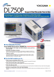
1
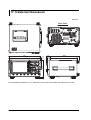
Chapter 17 Specifications
17.1 Input Section
Item
Specifications
Number of input channels
DL7440 (4-channel model, models 7071450 and 701460): 4 (CH1 to CH4)
DL7480 (8-channel model, models 7071470 and 701480): 8 (CH1 to CH8/4)
Input coupling
AC 1MΩ, DC 1MΩ, DC 50Ω, and GND
Input connector
BNC connector
Input impedance
1 MΩ±1.0%, approx. 20 pF
50 Ω±1.0% (VSWR 1.4 or less (DC to 500 MHz))
Voltage-axis sensitivity setting
For 1MΩ input:
For 50 Ω input:
Maximum input voltage
For 1 MΩ input (at a frequency of 1 kHz or less): 400 V (DC+ACpeak) (282 Vrms CAT II)
For 50 Ω input:
5 Vrms and 10 Vpeak (not to exceed either of the two values)
Maximum DC offset setting range
(When the probe attenuation
is set to 1:1)
2 mV/div to 50 mV/div:
±1 V
100 mV/div to 500 mV/div: ±10 V
1 V/div to 10 V/div:
±100 V
Vertical (voltage) axis accuracy
DC accuracy1:
Offset voltage axis accuracy1
2 mV/div to 10 V/div (1-2-5 steps)
2 mV/div to 1 V/div (1-2-5 steps)
±(1.5% of 8 div + offset voltage axis accuracy)
2 mV/div to 50 mV/div:
±(1% of the setting + 0.2 mV)
100 mV/div to 500 mV/div: ±(1% of the setting + 2 mV)
1 V/div to 10 V/div:
±(1% of the setting + 20 mV)
Frequency characteristics1, 2
(–3 dB point when a sine wave of
amplitude ±4 divisions is input)
For 50 Ω input
1 V/div to 10 mV/div:
DC to 500 MHz
5 mV/div to 2 mV/div:
DC to 400 MHz
For 1 MΩ input (when using the 700988 passive probe, indicates the frequency of the input
signal at the probe tip)
10 V/div to 10 mV/div:
DC to 400 MHz
5 mV/div to 2 mV/div:
DC to 300 MHz
Lower –3 dB point when AC
coupled
10 Hz or less (1 Hz or less when using the 10:1 probe provided)
Skew between channels
(When using the same settings)
1 ns or less
Residual noise level3
±1.25 mV or ±0.15 div, whichever is greater (typical value4)
Isolation between channels
(Same voltage sensitivity)
At 500 MHz: –34 dB (typical value4)
A/D conversion resolution
8 bits (24 LSB/div)
Probe attenuation setting
1:1, 10:1, 100:1, 1000:1, 10A:1V5, and 100A:1V5
Bandwidth limit
Turn ON/OFF the 100-MHz or 20-MHz bandwidth limit for each channel.
Maximum sample rate
Realtime sampling mode
When interleave mode is ON:
When interleave mode is OFF:
Repetitive sampling mode:
Maximum record length
2
3
4
5
4 MW memory model (701450 and 701470)
When interleave mode is ON:
4 MW/CH
When interleave mode is OFF: 2 MW/CH
16 MW memory model (701460 and 701480)
When interleave mode is ON:
16 MW/CH
When interleave mode is OFF: 8 MW/CH
Value measured under standard operating conditions (see section 17.12) after warm-up and after calibration with the time
base set to internal clock.
Value in the case of a repetitive phenomenon. The frequency bandwidth of a single-shot phenomenon is the smaller of the
two values, DC to sampling frequency/2.5 and the frequency bandwidth of a repetitive phenomenon.
When the input section is shorted, the record length set to 10 kW, the acquisition mode set to normal mode, the
accumulation set to OFF, and the probe attenuation set to 1:1.
Typical value represents a typical or average value. It is not strictly warranted.
Automatically set to the optimum values for the current probe (700937, 701930, or 701931, sold separately).
IM 701450-01E
17-1
Specifications
1
2 GS/s
1 GS/s
100 GS/s
17
17.2 Logic Input Section (Optional)
Item
Specifications
7019801/701981 (8-bit input)
Probes that can be used
2
Maximum toggle frequency
When using the 701980: 100 MHz, when using the 701981: 250 MHz
Number of inputs
16 (when two logic probes are used)
Maximum input voltage
±40 V (DC+ACpeak) or 28 Vrms when the frequency is 1 kHz or less.
Input range
±10 V
Maximum sample rate
When interleave mode is ON: 2 GS/s
When interleave mode is OFF: 1 GS/s
Threshold level
When using the 701980: ±40 V (resolution: 0.1 V)
When using the 701981: ±10 V (resolution: 0.1 V)
±(0.1 V + 3% of the setting)
Threshold accuracy2
Minimum input voltage
2
500 mVp-p
Input impedance
When using the 701980: Approx 1 MΩ/approx. 10 pF
When using the 701981: Approx. 10 kΩ, approx. 9 pF
Preset threshold levels
CMOS (5 V): 2.5 V, CMOS (3.3 V): 1.6 V, and ECL: –1.3 V
1
2
The 701980 can be used only when the firmware version of the DL7400 is 1.30 or later.
Under standard operating conditions (see section 17.12) after the warm-up.
17.3 Trigger Section
Item
Specifications
Trigger mode
Auto, auto-level, normal, single, and single(N)
Trigger source
CH1 to CH8/41 (signal input from each input terminal), LINE (commercial power supply
signal that is connected),
EXT (signal input from the EXT TRIG IN terminal)
Trigger coupling
CH1 to CH8/41:
EXT:
HF rejection
Select the bandwidth limit with respect to the trigger source (OFF, DC to approx. 15 kHz, or
DC to approx. 20 MHz) for each channel (CH1 to CH8/41)
Trigger hysteresis
Select high or low for the trigger level hysteresis width for each channel (CH1 to CH8/41)
Trigger level range
CH1 to CH8/41:
EXT:
±4 divisions from the screen center (resolution of 0.01 divisions)
±2 V (resolution is 5 mV)
Trigger level accuracy
CH1 to CH8/41, 2:
EXT3:
±(1 division + 10% of the trigger level)
±(50 mV + 10% of the trigger level)
Probe attenuation setting for
external trigger
1:1 or 10:1
Trigger sensitivity3
CH1 to CH8/41:
EXT:
DC/AC
DC
1 divP-P at DC to 500 MHz
100 mVP-P at DC to 100 MHz
Trigger position
Can be set in 1% increments of the display record length.
Trigger delay range
0 to 4 s
Hold off time range
80 ns to 10 s
Trigger slope
Rising, falling, rising and falling (for edge trigger)
17-2
IM 701450-01E
17.3 Trigger Section
Item
Specifications
Trigger type
Edge:
A->B(N):
Trigger gate
Trigger can be activated only when the trigger condition is met when the input from the
trigger gate input terminal (TRIG GATE IN) is active.
Active level can be set to high or low.
Specifications
1
2
3
4
5
Activate the trigger on the edge of a single trigger source.
Trigger occurs nth time condition B becomes true after condition A becomes
true.
Count:
1 to 108
Condition A:
Enter/Exit
Condition B:
Enter/Exit
A Delay B: Trigger occurs first time condition B becomes true after specified delay
following condition A true.
Specified time: 3 ns to 5 s
Condition A:
Enter/Exit
Condition B:
Enter/Exit
OR:
Trigger occurs on the OR logic of the trigger conditions set to multiple trigger
sources.
Trigger condition is edge or window. Rise (IN), Fall (Out), or Don’t Care can
be set to each channel CH1 to CH8/41.
Pattern:
Trigger occurs on the edge of the clock channel with respect to the True/False
condition of the parallel pattern set to multiple trigger sources. If the clock
channel is set to Don’t Care, trigger occurs on the Enter or Exit condition of
the True/False condition of the parallel pattern.
Parallel pattern is the AND of the channels.
Width:
Trigger occurs on the True/False width of the parallel pattern of multiple trigger
sources.
Parallel pattern is the AND of the statuses of the channels or the AND of the
window conditions of the channels.
Pulse<Time:
Trigger occurs when the width described
above is smaller than Time.
Pulse>Time:
Trigger occurs when the width described
above is greater than Time.
T1<Pulse<T2:
Trigger occurs when the width described
above is greater than T1 and smaller than
T2.
Time Out:
Trigger occurs when the width described
exceeds Time.
Specified time:
1 ns to 1 s
±(0.5% of the setting4 + 1 ns)
Time accuracy2:
Minimum time detection width2: 2 ns (typical value5)
TV:
Activates a trigger on the video signal of various formats: NTSC, PAL,
SECAM, 1080/60i, 1080/50i, 720/60p, 480/60p, 1080/25p, 1080/24p, 1080/
24sF, and 1080/60p CH1 is the only input channel. Field number and line
number selectable.
Logic:
Trigger occurs on the edge of the clock bit with respect to the True/False
condition of the parallel pattern of multiple logic inputs.
If the clock bit is set to Don’t Care, trigger occurs on the Enter or Exit condition
of the True/False condition of the parallel pattern.
Parallel pattern is the AND of the statuses of the bits of Pod A and B (16 bits)
Clock bit is an arbitrary bit of Pod A and B (16 bits).
• Condition A and Condition B are parallel patterns set using High, Low, and Don’t Care on
each channel CH1 to CH8/41.
The maximum number of channels varies depending on the model.
Under standard operating conditions (see section 17.12) after the warm-up and calibration.
Under standard operating conditions (see section 17.12) after the warm-up.
The value of T2 for T1<Pulse<T2.
Typical value represents a typical or average value. It is not strictly warranted.
17
IM 701450-01E
17-3
17.4 Time Axis
Item
Specifications
Time axis range
1 ns/div to 50 s/div (when the record length is greater than or equal to 10 kW)
1 ns/div to 5 s/div (when the record length is equal to 1 kW)
Time base accuracy1
±(0.005%)
Time axis precision1
±(0.005% + 50 ps + 1 digit)2
External clock input
(EXT CLOCK IN)
Connector type
Maximum input voltage
Input frequency range
Sampling jitter
Minimum input amplitude
Threshold level
Input impedance
Minimum pulse width
1
2
BNC
±40 V (DC+ACpeak) or 28 Vrms when the frequency is 10 kHz
or less.
40 Hz to 20 MHz (continuous clock only)
±1.25 ns or less
0.1 VP-P
±2 V (resolution is 5 mV)
Approx. 1 MΩ and 22 pF
10 ns or more for high and low.
Under standard operating conditions (see section 17.12) after the warm-up.
1 digit is the amount of time that cannot be determined due to sampling error.
17.5 Display
Item
Specifications
Display
8.4" color TFT LCD monitor
Display screen size
170.9 mm (width) × 129.6 mm (height)
Total number of pixels*
640×480
Display resolution of the
waveform display
500×384
*
Liquid crystal display may include few defective pixels (within 20 ppm with respect to the total number of pixels including RGB).
There may be few pixels on the liquid crystal display that do not turn ON all the time or remains ON all the time. Note that
these are not malfunctions.
17.6 Function
Acquisition and Display
Item
Specifications
Acquisition mode
Select from 4 acquisition modes: normal, envelope, averaging, and box average.
Sampling mode
Switch between realtime sampling and repetitive sampling at some of the time axis settings.
Record length
1 kW, 10 kW, 50 kW, 100 kW, 250 kW, 500 kW, 1 MW, 2 MW, 4 MW, 8 MW, and 16 MW (8
MW and 16 MW are available only on the 16 MW memory model.)
Zoom
Expand the displayed waveform along the time axis (up two locations using separate zoom rates)
Display format
Split display of analog waveforms (1, 2, 3, 4, 6, and 8 windows (1, 2, 3, 4, and 6 windows on
the 4-channel model) and a logic window for logic waveforms (optional).
Display interpolation
Select interpolation OFF (dot display of sample points), sine interpolation display, linear
interpolation display, or pulse interpolation display.
Graticule
Select from three graticule types.
Auxiliary display ON/OFF
Turn ON/OFF the scaled values and waveform labels.
X-Y display
Displays two X-Y waveforms of XY1 and XY2.
Accumulation
Accumulates waveforms on the display. Select persistence mode or color grade mode.
Snapshot
Retains the current displayed waveform on the screen. Snapshot waveforms can be saved
and loaded.
Clearing traces
Clears the displayed waveform.
17-4
IM 701450-01E
17.6 Function
Vertical and Horizontal Axes
Item
Specifications
Channel ON/OFF
ON/OFF on each channel CH1 to CH8/4*
Input filter
Set 100-MHz or 20-MHz bandwidth limit on each channel CH1 to CH8/4*.
Vertical position
Waveforms can be moved vertically in the range of ±4 div from the center of the waveform display frame.
Linear scaling
Set the scaling factor, offset value, and unit on each channel CH1 to CH8/4*.
Roll mode
Roll mode display is enabled when the trigger mode is set to auto, auto level, or single at the
following time axis settings.
1 MW or less: 50 ms/div to 50 s/div (except 50 ms to 5 s/div for 1kW)
2 MW:
100 ms/div to 50 s/div
4 MW:
200 ms/div to 50 s/div
8 MW:
500 ms/div to 50 s/div
16 MW:
1 s/div to 50 s/div
*
The maximum number of channels varies depending on the model.
Computation, Analysis, and Search
Item
Specifications
Computation
+, –, ×, binary computation, invert, differentiation, integration, and power spectrum.
The maximum record length that can be computed is as follows:
4 MW memory model (701450 and 701470):
All record lengths.
16 MW memory model (701460 and 701480): 8 MW when interleave mode is ON
4 MW when interleave mode is OFF
However, select the range (1 kW or 10 kW) for power spectrum computation (FFT).
Phase shift
Waveforms can be observed by shifting the phase of CH1 to CH8/41. Computation is performed using
the phase-shifted waveforms. The maximum record length that can be phase shifted is 8 MW.
User-defined computation Equations obtained by arbitrarily combining the following operators.
(optional)
+, –, ×, /, ABS, SQRT, LOG, EXP, NEG, SIN, COS, TAN, ATAN, PH, DIF, DDIF, INTG, IINTG, BIN,
P2, P3, F1, F2, FV, PWHH, PWHL, PWLH, PWLL, PWXX, DUTYH, DUTYL, FILT1, FILT2, HLBT,
MEAN, LS-, PS-, PSD-, CS-, TF-, CH-, MAG , LOGMAG, PHASE, REAL, and IMAG
The maximum record length is the same as the normal computation shown above. However,
computation is performed on up to 2 MW from the computation start point.
Search for and display waveforms from the history memory that meet specified conditions.
Select the search method from the following two types.
Zone:
Set an area on the screen, then extract and display only those waveforms that pass through
the area (Pass mode), or do not pass through the area (Bypass mode).
Parameter: Extract and display only the results of the automated measurement of waveform
parameters that meet the specified condition.
Search & zoom
Search a section of the displayed waveform data and display the section expanded.
Select the search method from the following five types.
Edge:
Counts the rising and falling edges and automatically searches an arbitrary edge.
Serial pattern: Automatically searches serial patterns of up to 64 bits synchronized or not
synchronized to the clock.
Parallel pattern: Automatically searches parallel patterns of CH1 to CH8/41, MATH1, MATH2, and
16 bits of logic (optional).
Pulse width:
Automatically searches the locations where the pulse width meets the specified condition.
Auto scroll:
The zoom position can be automatically scrolled.
Cursor measurements
The following cursors are selectable.
Horizontal, Vertical, Marker, and Degree
Automated measurement
of waveform parameters
Capable of performing automated measurement of waveform parameters.
Automated measurement of waveform parameters within one cycle (P-P through Int2XY), statistical
processing of waveform parameters, and statistical processing on the waveform parameters of
historical data.
P-P, Max, Min, Avg, Rms, Sdev, High, Low, +OShot, –OShot, Int1TY, Int2TY, Int1XY, Int2XY, Freq, Period,
Rise, Fall, +Width, –Width, Duty, Burst1, Burst2, Pulse, AvgFreq, AvgPeriod, and Delay (between channels)
Statistical processing results
Statistics:
Min, Max, Avg, Cnt, and Sdv
Measurement of waveform parameters in dual areas is also possible.
Computation can be performed between waveform parameters measured in dual areas and
constants. Operators are +, -, *, and /.
GO/NO-GO determination The following two types of GO/NO-GO determination are available
• Determination using zones on the screen
• Determination using the result of the automated measurement of waveform parameters
Specify an action for NO-GO result. Possible actions are screen image data output, waveform data
storage, buzzer notification, and e-mail transmission2.
IM 701450-01E
17-5
Specifications
History search
17
17.6 Function
Item
Specifications
SPI signal analysis/search
Data analysis and search by applying Clock to CH1, Data1 to CH2, Data2 to CH3, and CS
signals to CH4 to CH81 or bit 0 to bit 7 of logic input (optional) Pod A.
Analysis function: Display the status of Data1, Data2, and CS in unit of bytes (8 bits) of
serial data. The analysis results can be output to a file.
Search function:
Search arbitrary or specific data patterns based on the analysis results.
1
2
The maximum number of channels varies depending on the model.
When the Ethernet interface option is installed.
Saving and Printing of the Screen Image Data
Item
Specifications
Built-in printer (optional)
Prints screen image data.
External printer
Outputs the screen image to an external printer via the USB PERIPHERAL terminal or the
Ethernet network1. Supports page description languages and printer types such as ESC/P,
ESC/P2, LIPS3, PCL5, Post Script (only via the Ethernet network1), and BJ
Floppy disk or Zip disk2, SCSI3,
network drive1, and PC card
Output data format: PostScript, TIFF, BMP, JPEG, and PNG
1
2
3
When the Ethernet interface option is installed.
Select the floppy disk drive or Zip drive for the built-in storage medium drive at the time of purchase.
When the SCSI option is installed.
Data Storage
Item
Specifications
History memory
When interleave mode is ON: Automatically save up to 4096 acquisition data points.
When interleave mode is OFF: Automatically save up to 2048 acquisition data points.
Floppy disk or Zip disk1, SCSI2,
network drive3, and PC card
Saves setup data, waveform data, and various data
1
2
3
Select the floppy disk drive or Zip drive for the built-in storage medium drive at the time of purchase.
When the SCSI option is installed.
When the Ethernet interface option is installed.
Other Functions
Item
Specifications
Initialization
Resets settings to the factory default (excluding date/time setting, communication interface
settings, SCSI ID number setting, settings stored to the internal memory using the store/
recall function, and language setting)
Auto setup
Automatically set the optimum voltage axis, time axis, trigger, and other settings for the
input signal.
Store/Recall
Store to and recall from the DL7400 internal memory up to three sets of arbitrary setup data.
Preset
Presets for CMOS (5 V), CMOS (3.3 V), ECL, and user settings.
Action-on-trigger
Output screen image data, saves waveform data, activates buzzer notification, or sends email messages each time a trigger occurs.
Mail transmission1
Periodically send the status of the DL7400 to a specified mail address via the Ethernet
network. Can also send information as an action for GO/NO-GO determination and actionon-trigger.
Calibration
Auto calibration and manual calibration available.
Deskew
Correct the delay of the acquired waveforms on each channel.
Adjustment range is ±100 ns (0.01 ns resolution)
Environment settings
Set the screen color, date/time, message language, and click sound ON/OFF
Probe compensation signal output Outputs a signal (rectangular signal of approx. 1 Vp-p and approx. 1 kHz) from the probe
compensation output terminal on the front panel
Overview
Check the system status of the DL7400.
Self test
Memory test, key test, printer test, FDD/Zip drive2 test, SCSI test, and accuracy test are possible.
Help
Displays help concerning the settings (select English or Japanese)
Thumbnail
Shows thumbnails of the screen image data
1
2
17-6
When the Ethernet interface option is installed
Select the floppy disk drive or Zip drive for the built-in storage medium drive at the time of purchase.
IM 701450-01E
17.7 Built-in Printer (Optional)
Item
Specifications
Printing system
Thermal line dot system
Dot density
8 dots/mm
Paper width
112 mm
17.8 Storage
Built-in Floppy Disk Drive*
Item
Specifications
Number of drives
1
Size
3.5 inch
Capacity
1.44 MB
*
Select the floppy disk drive or Zip drive for the built-in storage medium drive at the time of purchase.
Built-in Zip Drive*
Item
Specifications
Number of drives
1
Capacity
100 MB or 250 MB
*
Select the floppy disk drive or Zip drive for the built-in storage medium drive at the time of purchase.
SCSI (Optional)
Item
Specifications
Standard
Conforms to ANSIX3.131-1986 for SCSI (Small Computer System Interface)
Connector
Half pitch 50 pins
Connector pin assignment
Unbalanced (single-ended)
PC Card Interface
Item
Specifications
Number of slots
1
Supported cards
Flash ATA memory card (PC card TYPE II)
17.9 Keyboard, Printer, and Mouse Interfaces
Specifications
Item
Specifications
Connector type
USB type A connector (receptacle)
Electrical and mechanical
specifications
Conforms to USB Revision 1.0
Supported keyboards
104 keyboard (US), 109 keyboard (Japanese), and 89 keyboard (US and Japanese)
conforming to USB HID Class Version 1.1
Supported printers
ESC/P, ESC/P2, LIPS3, PCL5, and BJ (can be used on models that support the BJC-35V
native commands) that support USB (USB Printer Class Version 1.0)
Supported mouse
Mouse conforming to USB HID Class Version 1.1
Power supply
5 V, 500 mA (per port)
Number of ports
2
IM 701450-01E
17-7
17
17.10 Auxiliary I/O Section
External Trigger Input1 and Trigger Gate Input1
Item
Specifications
Connector type
Input bandwidth
BNC
2
DC to 100 MHz3
Input impedance
Approx. 1 MΩ and 22 pF
Maximum input voltage
±40 V (DC+ACpeak) or 28 Vrms when the frequency is 10 kHz or less.
Trigger level
±2 V (resolution of 5 mV)
1
2
3
The external trigger input terminal (EXT TRIG IN)/trigger gate input terminal (TRIG GATE IN) is also used as an external
clock input terminal (EXT CLOCK IN). See the specifications of the external clock input (see section 17.4).
Under standard operating conditions (see section 17.12) after the warm-up.
The input frequency range when using the terminal as a trigger gate input is DC to 50 MHz.
Trigger Output (TRIG OUT)
Item
Specifications
Connector type
BNC
Output level
TTL
Output logic
(Negative)
Output delay time
50 ns max
Output hold time
1 µs minimum for low level and 100 ns minimum for high level
RGB Video Signal Output (VIDEO OUT)
Item
Specifications
Connector type
15-pin D-Sub receptacle
Output type
VGA compatible
Probe Power Supply Terminal
Item
Specifications
Number of output terminals
4 (A to D)
(4 optional terminals (E to H) can be added on the 8-channel model).
Output voltage
+12 V (Up to ±500 mA on each pair of terminals A and E; B and F; C and G; and D and H.)
Probes that can be used
FET probe (700939), current probe (700937, 701930, or 701931), and differential probe
(701920 or 701922)
17-8
IM 701450-01E
17.11 Computer Interface
GP-IB
Item
Specifications
Electrical and mechanical
specifications
Conforms to IEEE St’d 488-1978 (JIS C 1901-1987).
Functional specifications
SH1, AH1, T5, L4, SR1, RL1, PP0, DC1, DT0, and C0
Protocol
Conforms to IEEE St’d 488.2-1987.
Code
ISO (ASCII) code
Mode
Addressable mode
Address
Specify a talker/listener address between 0 and 30.
Clear remote mode
Remote mode can be cleared using the SHIFT+CLEAR key (except during Local Lockout).
USB
Item
Specifications
Connector type
USB type B connector (receptacle)
Electrical and mechanical
specifications
Conforms to USB Revision 1.0.
Data rate
12 Mbps max.
Number of ports
1
PC system supported
PC running Windows 98 SE, Windows Me, Windows 2000, or Windows XP with a standard
USB port (a separate driver is needed to connect to a PC).
Ethernet (Optional)
Item
Specifications
Number of communication ports
1
Electrical and mechanical
specifications
Conforms to IEEE802.3.
Transmission system
Ethernet (100BASE-TX/10BASE-T)
Transmission rate
100 Mbps max.
Communication protocol
TCP/IP
Supported services
FTP server, FTP client (network drive), LPR client (network printer), SMTP client (mail
transmission), Web server, DHCP, DNS, SNTP*, and WebDAV*
Connector type
RJ-45 connector
*
SNTP and WebDAV are available only on models with a firmware version of 1.30 or later.
Specifications
17
IM 701450-01E
17-9
17.12 General Specifications
Item
Specifications
Standard operating conditions
Ambient temperature: 23±2°C
Ambient humidity:
55±10% RH
Error in supply voltage and frequency:
Warm-up time
At least 30 minutes
Storage conditions
Temperature:
Humidity:
–20 to 60°C, –20 to 50°C (for the -J2: built-in Zip drive model)
20 to 80% RH (no condensation)
Operating Conditions
Temperature:
Humidity:
5 to 40°C
20 to 80% RH (when the printer is not used) (no condensation)
35 to 80% RH (when the printer is used) (no condensation)
Storage altitude
3000 m or less
Operating altitude
2000 m or less
Rated supply voltage
100 to 120 VAC/220 to 240 VAC
Within 1% of rating
Permitted supply voltage range
90 to 132 VAC/198 to 264 VAC
Rated supply voltage frequency
50/60 Hz
Permitted supply voltage
frequency range
48 to 63 Hz
Power fuse
250 V/6.3 A time lag, VDE/SEMKO/UL/CSA certified.
Inside the case. Cannot be replaced by the user.
Maximum power consumption
320 VA
Withstanding voltage
1.5 kVAC for one minute.
(between power supply and case)
Insulation resistance
10 MΩ or more at 500 VDC.
(between power supply and case)
External dimensions
(details on the next page)
373 mm (W) × 210.5 mm (H) × 355.3 mm (D)
(When the printer cover is closed. Excludes the handle and other projections.)
Weight
Approx. 10 kg
(only the main unit without the printer)
Instrument’s cooling method
Forced air cooling, exhaust from rear.
Installation position
Horizontal (the stand can be used to tilt the DL7400), stacking prohibited.
Recommended calibration period
1 year
Battery backup
Setup data and clock are backed up with the internal lithium battery
Battery life:
Approx. 5 years (at ambient temperature of 23°C)
Standard accessories
•
•
•
•
•
•
•
•
•
•
17-10
Power Cord:
400 MHz passive probe:
Soft case:
Front panel protection cover:
Printer roll paper:
Rubber feet:
User’s manual:
Operation guide:
Communication Interface User’s Manual:
Power Supply Analysis Function User’s Manual:
1 piece
4 pieces
B9969ET, 1 piece
B8051DP, 1 piece
1 roll (for /B5 suffix code)
4 pieces (2 A9088ZM)
1 piece
1 piece
1 piece (CD-ROM)
1 piece (for /G4 suffix code)
IM 701450-01E
17.12 General Specifications
Item
Specifications
Safety Standards
Complying standards
EN61010-1
• Overvoltage category II1
• Pollution degree 22
Emission
Complying standards
•
•
•
•
Cable condition
•
•
•
•
•
•
•
•
•
Immunity
2
3
4
•
EN61326 commercial environment (applies to 701450, 701460, 701470,
701480, 700988, 700939, and 701981)
Influence in the immunity environment
• Noise increase: ≤ ±200 mV (when using 700988)
≤ ±400 mV (when using 700939)
No influence (when using 701981)
• Test conditions
When using the 700988: 1 GS/s, envelope mode, 20 MHz BWL, 1 MΩ
input coupling, 50 mV/div (10:1 probe
attenuation setting), and 50-Ω termination at
the probe tip.
When using the 700939: 1 GS/s, envelope mode, 20 MHz BWL, 50 Ω
input coupling, 100 mV/div (10:1 probe
attenuation setting), 50-Ω termination at the
probe tip, and with a ferrite core (TDK:
ZCAT2035-0930A, YOKOGAWA: A1190MN)
attached to each end of the signal cable.
When using the 701981: 1 GS/s, envelope mode, and 50-Ω termination
at the probe tip.
• Cable condition
Same as the cable condition for emission above.
The Overvoltage Category (Installation Category) is a value used to define the transient overvoltage condition and includes
the impulse withstand voltage regulation. II applies to electrical equipment that is powered by a fixed installation such as a
distribution board.
Pollution Degree applies to the degree of adhesion of a solid, liquid, or gas which deteriorates withstand voltage or surface
resistivity. Pollution Degree 2 applies to normal indoor atmospheres (with only non-conductive pollution).
Use cables of length 3 m or less.
Use cables of length 30 m or less.
IM 701450-01E
17-11
Specifications
1
Complying standards
EN61326 Class A, C-Tick AS/NZS 2064 (applies to 701450, 701460,
701470, 701480, 700988, 700939, and 701981)
EN61000-3-2
EN61000-3-3
This product is a Class A (for commercial environment) product.
Operation of this product in a residential area may cause radio
interference in which case the user is required to correct the
interference.
External trigger input/external clock input/trigger gate input terminal
Use a BNC cable3 and attach a ferrite core (TDK: ZCAT2035-0930A,
YOKOGAWA: A1190MN) on one end (DL7400 end).
Trigger output terminal
Same as the external trigger input terminal above.
RGB video signal output (VIDEO OUT) terminal
Use a 15-pin D-Sub VGA shielded cable3.
SCSI connector
Use a SCSI shielded cable3 and attach a ferrite core (TDK: ZCAT20350930A, YOKOGAWA: A1190MN) on one end (DL7400 end).
USB PERIPHERAL connector
Attach a ferrite core (TDK: ZCAT1325-0530A, YOKOGAWA: A1181MN)
on one end (DL7400 end) of the USB cable3.
USB interface connector
Attach a ferrite core (TDK: ZCAT1325-0530A, YOKOGAWA: A1181MN)
on one end (DL7400 end) of the USB cable3.
Ethernet interface connector
Use a Ethernet interface cable4 and attach a ferrite core (TDK:
ZCAT2035-0930A, YOKOGAWA: A1190MN) on one end (DL7400 end).
Probe power terminal
Attach a ferrite core (TDK: ZCAT1325-0530A, YOKOGAWA: A1181MN)
on one end (DL7400 end) of the cable.
Logic probe input connector
Attach a ferrite core (TDK: ZCAT2035-0930A, YOKOGAWA: A1190MN)
on one end (DL7400 end) of the cable.
17
17.13 External Dimensions
Unit: mm
Rear View
A
B
C
D
E
F
G
H
100-120/220-240V AC
320VA MAX 50/60Hz
ETHERNET
ACT
VIDEO OUT
GP-IB(IEEE488)
100BASE-TX
SCSI
PROBE POWER
USB
LINK
A
(VGA)
B
USB
PERIPHERAL
WARNING
LOGIC PROBE
Do not operate within reading
safety precautions in user s manual.
TRIG OUT
EXT CLOCK IN
EXT TRIG IN
TRIG GATE IN
<40Vpk 1MΩ
14
40
31
349.6
324.3
20
210.5
374
373
If not specified, the tolerance is ±3%. However, in cases of less than 10 mm, the tolerance is ±0.3 mm.
17-12
IM 701450-01E