1
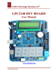
User Manual For CP-JR ARM7 USB-LPC2148 / EXP CP-JR ARM7 USB-LPC2148 / EXP 38 CR-JR ARM7 USB-LPC2148 which is a Board Microcontroller ARM7TDMI-S Core uses Microcontroller 16/32-Bit 64 Pin as Low Power type to be a permanent MCU on board and uses MCU No.LPC2148 from Philips. Especially, structure of Board is designed the arrangement of basic components that is necessary to learn, study, and test independently and perfectly, for example, LED to display status of Output Logic, Push Button Switch to create signal Logic for testing operation of Input or Volume to adjust Voltage for testing operation of A/D. These basic circuits are designed and arranged to be connecting point independently because it does not interface with any signal Pin of CPU. So, we can modify and adjust circuit preferably and can use circuit corresponding with resources inside CPU perfectly. For example, Signal Pin GPIO0.8 of LPC2148 can be configured up to 4 modes; Input/Output, TXD1, PWM and ADC, so if we want to test signal Pin GPIO0.8 with any mode, we can select to interface with signal Pin from GPIO0.8 into supported circuit suitably as follows; When we want to test GPUIO0.8 to be Input, we can interface signal Pin from GPIO0.8 into circuit Push Button Switch to test operation of Input. When we want to test GPUIO0.8 to be Output, we can interface signal Pin from GPIO0.8 into circuit LED to see status operation of Output. When we want to test GPUIO0.8 to be ADC, we can interface signal Pin from GPIO0.8 into circuit Volume to adjust Voltage to test reading voltage Analog. When we want to test GPUIO0.8 to be TXD1, we can interface signal Pin from GPIO0.8 into circuit Line Driver of RS232 to test sending data as RS232 type. Notice, we can adjust, configure, and modify the signal Pins of CPU independently and we can apply it with all functions perfectly. For structure of board, MCU is arranged with necessary components and signal Pin is arranged neatly to be external usage through Connector IDE 10 Pin under standard ETT. So, it can be interfaced with supported ETT components perfectly. Board requires external Power Supply +5VDC, or USB Port (incase of current not higher than 100mA while it is not in Enumerate USB state and not higher than 500mA while it has already in Enumerate USB state). Moreover, internal board has already provided circuit Regulate 3.3V/1A and internal board has Connector RS232 (UART0) 1 Port for downloading Hex File or RS232 communication in written Program Application. ETT CO.,LTD. -1- WWW.ETT.CO.TH User Manual For CP-JR ARM7 USB-LPC2148 / EXP Specifications of Board 1. 16/32-Bit MCU ARM7TDMI-S No. LPC2148 from Philips 2. Crystal 12.00 MHz; MCU can collect data maximum high speed 60 MHz if using with Phase-Locked Loop (PLL) internal MCU itself 3. Support In-System Programming (ISP) and In-Application Programming (IAP)through On-Chip Boot-Loader Software through Port UART0 (RS232) 4. +5VDC Power Supply by using external Connector CPA-2Pin or using Power Supply from USB Port (in case of using current not higher than 500mA) 5. Internal MUC has 512KB Flash Memory, 40KB Static RAM 6. Circuit USB standard 2.0 as Full Speed insides(USB Function has 32 End Point) 7. Maximum GPIO 47 I/O Pins can be interfaced with system I/O that is signal 5V and signal Pin GPIO can be used with other Functions as follows; Circuit SPI Serial Communication 2 Channel Circuit I2C Serial Communication 2 Channel 14 Circuit ADC 10 Bit and 1 Circuit DAC 10 Bit Circuit UART Full-Duplex 2 Channel; UART-0 standard 4 Pin ETT to be RS232 level and UART-1 to be TTL Level Timer 32-Bit 2 Channel(4 Input Capture/ 4 Output Compare), 6-Channel PWM Output, Watchdog Timer and Real Time Clock 8. There is a circuit as 4 Bit type from GPIO 1 [25..31] to interface with Character LCD and circuit to contrast the brightness of Monitor. 9. There is a circuit to interface with JTAG ARM 20 Pin standard for debugging as Real Time type. 10. There is a basically supported circuits for learning and testing that have already provided internal board (to be only installed in version CP-JR ARM7 LPC2148 EXP ) as follows; 4 LED Output as Sink Current type to display status of Output 4 Push Button Switch as Active Logic “0” type to test Input Logic 4 Volume for adjusting Voltage 0-3.3V to test operation of ADC 1 Mini Speaker to test sound Project Board version AD-100 with 360 points to be available area that can be interfaced a small circuit for using with CPU independently The connecting point of Power Supply +3.3V and GND to interface into other external circuits 11. Temperature -40 to +85 ºC ETT CO.,LTD. -2- WWW.ETT.CO.TH User Manual For CP-JR ARM7 USB-LPC2148 / EXP Structure of Board CP-JR ARM7 USB-LPC2148 / EXP 21 20 4 2 3 6 14 7 16 1 5 13 15 19 11 18 17 8 9 12 10 Figure displays feature of Board CP-JR ARM7 LPC2148 / EXP. ETT CO.,LTD. -3- WWW.ETT.CO.TH User Manual For CP-JR ARM7 USB-LPC2148 / EXP 7 6 4 17 8 18 9 16 19 14 15 11 10 3 2 5 1 13 12 Figure displays feature of Board CP-JR ARM7 LPC2148. 7 8 17 16 6 4 19 15 9 18 11 10 5 13 14 3 20 2 21 1 12 Figure displays feature of Board AR-JR ARM7 LPC2148 EXP. ETT CO.,LTD. -4- WWW.ETT.CO.TH User Manual For CP-JR ARM7 USB-LPC2148 / EXP • • • • • • • • • • • • • • • • • • • • • No.1 is Connector Port 1 [16..23] 8 Bit. No.2 is Connector Port 0 [2..7] 6 Bit. No.3 is Connector Port 0 [8..15] 8 Bit. No.4 is Connector Port 0 [16..23] 8 Bit. No.5 is Connector Port 0 [25..31] 7 Bit. No.6 is Resistor to contrast the brightness of LCD Monitor. No.7 is Connector Character LCD by using signal Port 1 [25..31] for connection. No.8 is Connector JTAG by using signal Port 1 [26..31] and Reset of CPU. No.9 is Connector RS232 for usage and Download Hex File into CPU. No.10 is Connector USB for connection with USB Hub version 2.0. No.11 is LED to display Power status from USB and display status of connection with USB. No.12 is Power +5VDC and GND to supply power into board. No.13 is LED to display status of Power Supply of Board No.14 Switch RESET to command Reset operation of CPU. No.15 is Switch LOAD for using with Switch RESET to Download Hex into CPU. No.16 is CPU No.LPC2148 from Philips to be a permanent CPU on board. No.17 is Crystal 12.000 MHz to input signal clock of LPC2148. No.18 is Crystal 32.768 KHz for Real Time Clock (RTC) internal LPC2148 itself. No.19 is the connecting point of battery holder box +3V (to be under board) to interface with RTC and store time value of RTC while it does not supply power into board. No.20 is Project Board version AD-100 with 360 points to interface circuit (to be only installed in version CP-JR ARM7 LPC2148 EXP). No.21 is a part of basic circuit I/O to test operation of CPU Functions (to be only installed in version CP-JR ARM7 LPC2148 EXP) as follows; o 4 LED as Sink Current type to display operation results of Output o 4 Push Button Switch to generate Logic for testing operation of Input o 4 Volume to adjust voltage 0.3V for testing operation of A/D o 1 Mini Speaker o Connecting point of Power Supply +3.3V and GND ETT CO.,LTD. -5- WWW.ETT.CO.TH User Manual For CP-JR ARM7 USB-LPC2148 / EXP LED LED which displays operation results of board must be interfaced as Sink Current type by using Power Supply +3.3V. It runs with Logic “0” (0V) and stops running with Logic “1” (+3.3V), in this case there are 4 sets. We use this circuit to test operation of Port I/O that gives result as Output Logic type. +3.3V LEDn 560 LEDn Circuit to adjust Voltage (0V-3.3V) It is a circuit to adjust Voltage of board that uses VR (Variable Resistor) and uses Power Supply +3.3V. In this case we configure Output to be Voltage range as 0V to +3.3V follow the VR. There are 4 sets to create Input Voltage and test operation of circuit A/D. +3V3 10K VOLn ETT CO.,LTD. -6- WWW.ETT.CO.TH User Manual For CP-JR ARM7 USB-LPC2148 / EXP Circuit Push Button Switch It is a circuit that uses circuit Switch as Push Button type with circuit Pull-Up and uses Power Supply +3.3V. If Switch is not be pressed, status Logic is “1”; on the other hand, if Switch is pressed, status Logic is “0”. There are 4 sets to test operation of I/O that must be controlled Circuit with Input Logic type. +3V3 10K SWn SWn Circuit Mini Speaker It is a circuit to generate sound that uses Mini Speaker and circuit NPN Transistor to drive current into speaker. It requires Power Supply +3.3V and runs with Logic “1” and stop running with Logic “0”. For its operation, it sends signal logic that is various frequencies into speaker and it will create frequency ranges as our desired. +3V3 Mini Speaker 1N4148 BC547 SPK 1 ETT CO.,LTD. 1K -7- WWW.ETT.CO.TH User Manual For CP-JR ARM7 USB-LPC2148 / EXP Circuit Power Supply Circuit power Supply can be used with DC +5V instantly. In the part of circuit Regulate 3.3V supplies power into CPU and all circuit I/O of board except Character LCD that uses Power Supply +5VDC from Connector Terminal 2 Pin for board. In case we do not use Character LCD, we only can use Power Supply from USB Port but board is not interfaced with other external components. USB Port can supply Power into board not higher than 100mA if it is not in Enumerate USB Function state and can supply Power into board not higher than 500mA after it has already been in Enumerate USB Function state. +VUSB 1N5819 +3V3 1N5819 1 2 1 0.1uF 2 100uF 560 3 Vout PWR 5V6 LD1086(3V3) Vin GND +5V +5VDC 47uF To interface with Character LCD To interface LCD, we can only use with Character LCD as 4 Bit type connection. We use signal from GPIO1.25 to GPIO1.31 for 7 Bit for connection and some Bit signal is interfaced into Connector JTAG. It interfaces signal cable from Connector of Port LCD into LCD Monitor. Remember, we must use the signal name as reference point and must interface all 14 signal cables corresponding with all 14 truly names as in the figure below. +5V 10K P1.25 P1.27 P1.29 P1.31 +5V RS EN D1 D3 D5 D7 1 3 5 7 9 11 13 2 4 6 8 10 12 14 GND VO RW D0 D2 D4 D6 ET-CLCD +VCC RS EN P1.26 P1.28 P1.30 GND VO RW D1 D3 D5 D0 D2 D4 D7 D6 ET-CLCD ETT CO.,LTD. -8- WWW.ETT.CO.TH User Manual For CP-JR ARM7 USB-LPC2148 / EXP Connector Port I/O of board Connector Port I/O of CPU is arranged as IDE 10 Pin for 5 sets that has 8 Bit per a set as follows; NC NC P0.8 P0.9 P0.2 P0.3 P0.10 P0.11 P0.4 P0.5 P0.12 P0.13 P0.6 P0.7 P0.14 P0.15 +3V3 GND +3V3 GND PORT0[2..7] PORT0[8..15] P0.16 P0.17 NC P0.25 P0.18 P0.19 P0.26 P0.27 P0.20 P0.21 P0.28 P0.29 P0.22 P0.23 P0.30 P0.31 +3V3 GND +3V3 GND PORT0[16..23] PORT0[25..31] P1.16 P1.18 P1.17 P1.20 P1.21 P1.22 P1.23 +3V3 GND P1.19 PORT1[16..23] ***Note*** - GPIO0.0 is reserved to be TXD of UART0 (RS232) - GPIO0.1 is reserved to be RXD of UART0 (RS232) - GPIO1.25 to GPIO1.31 is reserved to interface with Character LCD. -GPIO0.23, GPIO0.26, GPIO0.27 and GPIO0.31 are reserved to be connection with USB. ETT CO.,LTD. -9- WWW.ETT.CO.TH User Manual For CP-JR ARM7 USB-LPC2148 / EXP Connector JTAG ARM JTAG or JTAG ARM is Connector IDE 20 Pin to interface with JTAG Debugger. Circuit and signal are arranged under standard of JTAG as follows; +3V3 100K * 4 +VTref TRST TDI TMS TCK RTCK TDO RESET# P1.31 P1.28 P1.30 P1.29 P1.26 P1.27 RES# RUN/D EB 1 3 5 7 9 11 13 15 17 19 2 4 6 8 10 12 14 16 18 20 +VTarget GND GND GND GND GND GND GND GND GND ARM-JTAG 10K 100K 10K VTref VTarget TRST TDI TMS GND GND GND TCK RTCK GND GND TDO RES# GND GND NC NC GND GND ARM JTAG Pin Connector Connector RS232 Port RS232 is signal RS232 level that has already transformed to be signal Level of MAX232, so it can be connected with signal RS232 to send/receive data. Additionally, it can be used with Switch LOAD and Switch RESET to Download Hex File into CPU. 1 2 3 4 +3V3 RXD TXD GND RS232 Connector Power Input (+5V) It is connecting point of Power Supply +5V for board and GND; we only input DC +5V. This Connector is arranged as follows; 2 +5V GND 1 ETT CO.,LTD. -10- WWW.ETT.CO.TH User Manual For CP-JR ARM7 USB-LPC2148 / EXP To Download Hex File into MCU of Board We use program LPC2000 Flash Utility from Philips to download Hex File into Flash memory of MCU on board. This program can be connected with MCU through Serial Port of computer PC. We can download free without any charge from www.semiconductors.philips.com Proceeding to Download Hex File into MCU 1. Interface RS232 cable between RS232 Serial Port Communication of PC and Board (RS232) 2. Supply Power +5VDC into board through Connector CPA 2 Pin (or through USB Port in case of USB Port can supply Power into Board) and we can notice that red LED (PWR) is in status ON. 3. Run Program LPC2000 Flash Utility from Philips and it will display result as in the picture below. 1 2 4 3 4. Configure default values into program as desired. In this case, we use LPC2148 of Board CP-JR ARM LPC2148 from ETT, we can configure default values follows these sample; 1) Select COM Port and it must be corresponding with COM Port number that is truly usage. 2) Set Baud Rate range as 4800–38400 that is tested and we can use it instantly without any error or we can use the standard speed value that is 9600. 3) Set Crystal Oscillator corresponding with truly usage internal board and set unit of it’s as KHz ETT CO.,LTD. -11- WWW.ETT.CO.TH User Manual For CP-JR ARM7 USB-LPC2148 / EXP as and not higher than 5 digits. In this case, we set it as 12.000 MHz that equal 12000. 4) Click button Read device ID to connect with CPU and then it will display message to access into Boot Mode as in the picture below. 5 5) Press Switch RESET and Switch LOAD on board CP- JR ARM7 LPC2148 to reset MCU running in Boot Loader Mode as the proceeding below; Press Switch LOAD for a while. Press Switch RESET and Switch LOAD remains pressing. Let Switch RESET but Switch LOAD remains pressing. Finally, let Switch LOAD and then click “OK”. 6) When it can connect CPU successfully, it will display detail of Part ID and Boot Loader ID as in the picture below. 7 8 6 7) Configure Hex programming ETT CO.,LTD. File -12- that we want to command WWW.ETT.CO.TH User Manual For CP-JR ARM7 USB-LPC2148 / EXP 8) Click “Upload to Flash” and program LPC2000 starts downloading data into MCU instantly. Notice that Status “Uploading to LPC2000 RAM and Copying to Flash Memory” as in the picture below and we must wait for the operation successfully by notice that Status “File Upload Successfully Completed”. 9 ↓ 9) When operation of program is successfully, press Switch RESET on board and MCU will start running follows by the downloaded program instantly. ETT CO.,LTD. -13- WWW.ETT.CO.TH