1
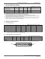
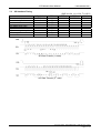
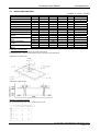
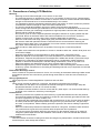
LMT035DNAFWU-1
LCD Module User Manual
Rev.
0.1
URL:
Descriptions
Preliminary New release
Release Date
2007-09-29
Document Name: LMT035DNAFWU-1-Manual-Rev0.1.DOC
Page: 1 of 10
LCD Module User Manual
LMT035DNAFWU-1
Table of Content
1.
APPLICATIONS ........................................................................................................................ 3
2.
General Specification .............................................................................................................. 3
3.
Block Diagram.......................................................................................................................... 3
4.
Terminal Function (Input Terminal) ....................................................................................... 4
5.
Absolute Maximum Ratings.................................................................................................... 5
6.
Electrical Characteristics........................................................................................................ 5
6.1
DC Characteristics ................................................................................................................................................. 5
6.2
LED Backlight Circuit Characteristics..................................................................................................................... 5
7.
AC Characteristics................................................................................................................... 6
7.1
Pixel Timing ........................................................................................................................................................... 6
7.2
SPI Interface Timing............................................................................................................................................... 7
7.3
Optical Characteristics ........................................................................................................................................... 8
8.
Precautions of using LCD Modules ....................................................................................... 9
9.
Appendix A <Inspection items and criteria for appearance defect>................................. 10
URL:
Document Name: LMT035DNAFWU-1-Manual-Rev0.1.DOC
Page: 2 of 10
LCD Module User Manual
LMT035DNAFWU-1
1. APPLICATIONS
This Module is designed for potable DVD, GPS car TV & PMP(portable multimedia player)
application which require high quality flat panel displays. It is also a good substitute for many
outmoded CSTN module in the industrial application.
This product is composed of a TFT-LCD panel, driver ICs, FPC and LED backlight unit.
2. General Specification
Signal Interface :
Display Technology :
Display Mode :
Screen Size(Diagonal) :
Outline Dimension :
Active Area :
Number of dots :
Pixel Pitch :
Pixel Configuration :
Backlight :
Surface Treatment :
Viewing Direction :
Operating Temperature :
Storage Temperature :
Digital 24-bits RGB
a-Si TFT active matrix
TN Type Full Color / Transmissive / Normal White
3.5”
96.7 x 63.9 x 3.7 (mm)
(see attached drawing for details)
70.08 x 52.56 (mm)
320 x 3 (RGB) x 240
0.219 x 0.219 (mm)
RGB Stripe
LED
Anti-Glare Treatment
12 o’clock
-20 ~ +70°C
-30 ~ +80°C
3. Block Diagram
VBL+, VBL-
Backlight Circuit
320(x3) x 240 pixels
TFT Panel
VCC
AVSS, GND
HSYNC, VSYNC, DCLK, ENB
R[0..7], G[0..7], B[0..7]
/RES, SPENA, SPCLK, SPDAT
Source Driver with TCON
HX8238A or equivalent
Power Circuit
Document Name: LMT035DNAFWU-1-Manual-Rev0.1.DOC
Page: 3 of 10
LCD Module User Manual
LMT035DNAFWU-1
4. Terminal Function (Input Terminal)
Pin No.
1
2
3
4
5
:
7
8
9
10
11
12
:
19
20
:
27
28
:
35
36
37
38
Pin Name
VBLVBLVBL+
VBL+
NC
:
NC
/RES
SPENA
SPCLK
SPDAT
B0
:
B7
G0
:
G7
R0
:
R7
HSYNC
VSYNC
DCLK
IO
Power
39
40
41
42
43
:
51
52
53
54
NC
NC
VCC
VCC
NC
:
NC
ENB
GND
AVSS
Descriptions
Negative Backlight Power Supply
Positive Backlight Power Supply
-
No Connection
Input
Input
Input
Input
Input
Hardware Reset
Serial port Enable (*1)
Serial port clock (*1)
Serial port Data input (*1)
8bit Data for Blue
Input
8bit Data for Green
Input
8bit Data for Red
Input
Input
Input
-
Horizontal Sync Input
Vertical Sync Input
Clock Signal for RGB data
Latching at the rising edge
No Connection
Power
Digital Power Supply
-
No connection
Input
Power
Power
Data Enable
Power GND (0V)
Power GND (0V)
Note:
*1 The SPI terminal is for Gamma and internal configuration.
*2 For digital RGB input data format, both SYNC mode and DE+SYNC mode are supported.
If ENB signal is fixed low, SYNC mode is used. Otherwise, DE+SYNC is used.
Document Name: LMT035DNAFWU-1-Manual-Rev0.1.DOC
Page: 4 of 10
LCD Module User Manual
LMT035DNAFWU-1
5. Absolute Maximum Ratings
Items
Supply Voltage
for Source Driver
Digital Input Voltage
Operating Temperature
Storage Temperature
Symbol
VCC
Min.
-0.3
Max.
+4.0
Unit
V
VIN
TOP
TST
-0.3
-20
-30
VDD+0.3
70
80
V
°C
°C
GND,VSS=0V, TOP=25°C
Condition
VSS = 0V
VSS = 0V
No Condensation
No Condensation
Note:
*1. This rating applies to all parts of the module. And should not be exceeded.
*2. Maximum wet-bulb temperature is 39 . Condensation of dew must be avoided.
*3. The operating temperature only guarantees operation of the circuit. The contrast, response speed,
and the other specification related to electro-optical display quality is determined at the room temperature, Ta=25.
*4. Ambient temperature when the backlight is lit (reference value)
*5 Any Stresses exceeding the Absolute Maximum Ratings may cause substantial damage to the device. Functional
operation of this device at other conditions beyond those listed in the specification is not implied and prolonged
exposure to extreme conditions may affect device reliability.
6. Electrical Characteristics
6.1
DC Characteristics
Items
Digital Supply Voltage
Digital Operating Current
Signal Input Voltage High
Signal Input Voltage Low
Frame Frequency
Dot Data Clock
Note:
*1.
6.2
Symbol
VCC
ICC
VSIG-H
VSIG-L
FFRAME
DCLK
GND,VSS=0V, VCC=3.3V, TOP=25°C
TYP.
MAX.
Unit
3.3
3.6
V
7.5
mA
VCC
V
0.2xVCC
V
60
Hz
6.5
MHz
MIN.
3.0
0.8xVCC
0
-
VCOMH& VCOML is for adjusting the color with gamma data
LED Backlight Circuit Characteristics
Items
Forward Voltage
Forward Current
Life Time
Symbol
VfBLA
IfBLA
-
MIN.
-
TYP.
20.0
20.0
50000
MAX.
22.0
-
VBL-= 0V, IfBL+=20mA, TOP=25°C
Unit Note
V
mA
hr
Cautions:
Exceeding the recommended driving current could cause substantial damage to the backlight and shorten its lifetime.
VBL+
VBLNo. of LED = 6 pcs
Document Name: LMT035DNAFWU-1-Manual-Rev0.1.DOC
Page: 5 of 10
LCD Module User Manual
LMT035DNAFWU-1
7. AC Characteristics
7.1
Pixel Timing
Item
DOTCLK Freq
DOTCLK Period
Vertical Sync Setup
Time
Vertical Sync Hold Time
Horizontal Sync Setup
Time
Horizontal Sync Hold
Time
Phase difference of Sync
Signal(falling edge)
DOTCLK Low Period
DOTCLK High Period
Data Setup Time
Data Hold Time
Reset Pulse width
Symbol
tdotclk
tdotclk
tvsys
MIN.
24bit
8bit
100
33.3
20
10
GND,VSS=0V, VCC=3.3V, TOP=25°C
TYP.
MAX.
Unit
24bit
8bit
24bit
8bit
6.5
19.5
10
30
MHz
154
51.3
ns
ns
tvsyh
thsys
20
20
10
10
-
-
-
-
ns
ns
thsyh
20
10
-
-
-
-
ns
thv
tclk
tckh
tsutdh
thd
tres
50
50
12
12
15
15
10
10
10
-
240
-
-
-
tdotclk
-
-
ns
ns
ns
ns
ns
Note: For the details of the timing, please see the Driver IC data sheet.
HSYNC / VSYNC / DCLK Timing Digram
RGB / DCLK / ENB Timing Diagram
Document Name: LMT035DNAFWU-1-Manual-Rev0.1.DOC
Page: 6 of 10
LCD Module User Manual
7.2
LMT035DNAFWU-1
SPI Interface Timing
Item
Serial Clock Freq
Serial Clock Cycle Time
Clock Low Width
Clock High Width
Chip Select Setup Time
Chip Select Hold Time
Chip Select High Delay Time
Data Setup Time
Data Hold Time
Symbol
fclk
tclk
tsl
tsh
tcss
tsch
tscd
tds
tdh
GND,VSS=0V, VCC=3.3V, TOP=25°C
TYP.
MAX.
Unit
20
MHz
ns
ns
ns
ns
ns
ns
ns
ns
MIN.
50
25
25
0
10
20
5
10
Note: the example below is transferring “1264h” into register ”28h”
SPI Data Transfer (1st data)
SPI Data Transfer (2nd data)
Document Name: LMT035DNAFWU-1-Manual-Rev0.1.DOC
Page: 7 of 10
LCD Module User Manual
7.3
LMT035DNAFWU-1
Optical Characteristics
If=20mA, VL=19.2V, Ta=25C
Item
Contrast Ratio
Luminance
Uniformity
Response Time Rise
Response Time Fall
Viewing Angle
Viewing Angle
Viewing Angle
Viewing Angle
Color Chromaticity
(White)
Color Chromaticity
(Red)
Color Chromaticity
(Green)
Color Chromaticity
(Blue)
Symbol
MIN.
TYP.
MAX.
CR
YL
LU
TR
TF
θl
θr
θu
θd
X
Y
X
Y
X
Y
X
Y
(250)
(200)
(70)
(50)
(50)
(40)
(40)
-
(300)
(250)
(75)
(10)
(15)
(60)
(60)
(50)
(60)
0.30
0.32
0.62
0.36
0.33
0.59
0.14
0.09
(20)
(30)
-
UNIT
Cd/m2
%
ms
ms
deg
deg
deg
deg
-
Note.
*1, θ=0
θ=0
*4, θ=0
*3, θ=0
*3, θ=0
*2
*2
*2
*2
Note:
*1. Definition of Contrast Ratio
The contrast ratio could be calculate by the following expression:
Contrast Ratio (CR) = Luminanc with all pixels white / Luminance with all pixels black
*2 Definition of Viewing Angle
*3 Definition of response time
Definition of Luminance Uniformity
Luminance uniformity (Lu)=
Min. Luminance form pt1~pt9 / Max Luminance form Pt1~pt9
Document Name: LMT035DNAFWU-1-Manual-Rev0.1.DOC
Page: 8 of 10
LCD Module User Manual
LMT035DNAFWU-1
8. Precautions of using LCD Modules
Mounting
- Mounting must use holes arranged in four corners or four sides.
- The mounting structure so provide even force on to LCD module. Uneven force (ex. Twisted stress)
should not applied to the module. And the case on which a module is mounted should have sufficient
strength so that external force is not transmitted directly to the module.
- It is suggested to attach a transparent protective plate to the surface in order to protect the polarizer.
It should have sufficient strength in order to the resist external force.
- The housing should adopt radiation structure to satisfy the temperature specification.
- Acetic acid type and chlorine type materials for the cover case are not desirable because the former
generates corrosive gas of attacking the polarizer at high temperature and the latter causes circuit
break by electro-chemical reaction.
- Do not touch, push or rub the exposed polarizers with glass, tweezers or anything harder than HB
pencil lead. Never rub with dust clothes with chemical treatment. Do not touch the surface of
polarizer for bare hand or greasy cloth.(Some cosmetics deteriorate the polarizer.)
- When the surface becomes dusty, please wipe gently with absorbent cotton or other soft materials
like chamois soaks with petroleum benzine. Normal-hexane is recommended for cleaning the
adhesives used to attach front / rear polarizers. Do not use acetone, toluene and alcohol because
they cause chemical damage to the polarizer.
- Wipe off saliva or water drops as soon as possible. Their long time contact with polarizer
Operating
- The spike noise causes the mis-operation of circuits. It should be within the ±200mV level (Over and
under shoot voltage)
- Response time depends on the temperature.(In lower temperature, it becomes longer.)
- Brightness depends on the temperature. (In lower temperature, it becomes lower.) And in lower
temperature, response time(required time that brightness is stable after turned on) becomes longer.
- Be careful for condensation at sudden temperature change. Condensation makes damage to
polarizer or electrical contacted parts. And after fading condensation, smear or spot will occur.
- When fixed patterns are displayed for a long time, remnant image is likely to occur.
- Module has high frequency circuits. Sufficient suppression to the electromagnetic interference shall
be done by system manufacturers. Grounding and shielding methods may be important to minimized
the interference
Electrostatic Discharge Control
Since a module is composed of electronic circuits, it is not strong to electrostatic discharge. Make certain
that treatment persons are connected to ground through wrist band etc. And don’t touch interface pin
directly.
Strong Light Exposure
Strong light exposure causes degradation of polarizer and color filter.
Storage
When storing modules as spares for a long time, the following precautions are necessary.
- Store them in a dark place. Do not expose the module to sunlight or fluorescent light. Keep the
temperature between 5°C and 35°C at normal humidity.
- The polarizer surface should not come in contact with any other object. It is recommended that they
be stored in the container in which they were shipped.
Protection Film
- When the protection film is peeled off, static electricity is generated between the film and polarizer.
This should be peeled off slowly and carefully by people who are electrically grounded and with well
ion-blown equipment or in such a condition, etc.
- The protection film is attached to the polarizer with a small amount of glue. If some stress is applied
to rub the protection film against the polarizer during the time you peel off the film, the glue is apt
tore main on the polarizer. Please carefully peel off the protection film without rubbing it against the
polarizer.
- When the module with protection film attached is stored for a long time, sometimes there remains a
very small amount of glue still on the polarizer after the protection film is peeled off.
- You can remove the glue easily. When the glue remains on the polarizer surface or its vestige is
recognized, please wipe them off with absorbent cotton waste or other soft material like chamois
soaked with normal-hexane.
Transportation
The LCD modules should be no falling and violent shocking during transportation, and also should avoid
excessive press, water, damp and sunshine.
Document Name: LMT035DNAFWU-1-Manual-Rev0.1.DOC
Page: 9 of 10
LCD Module User Manual
9.
Appendix A <Inspection items and criteria for appearance defect>
Items
Open Segment or Common
Short
Wrong Viewing Angle
Decliners
Contrast Ration Uneven
Crosstalk
White spots
Black Sport
Line Defect
Note:
1.
2.
LMT035DNAFWU-1
Criteria
Not permitted
Not permitted
Not permitted
Not permitted
According to the limit specimen
According to the limit specimen
Max 6 spots allowed
X>1 pixel
A-area
Not permitted
B-area
Max. 1 allowed
1/2 pixel<X≤1 pixel A-area
Not permitted
B-area
Max. 2 allowed
X≤1/2 pixel
A-area
Max. 1 allowed
B-area
Max. 4 allowed
X>1 pixel
A-area
Not permitted
B-area
Max. 2 allowed
X≤1/2 pixel
A-area
Max. 1 allowed
B-area
Max. 4 allowed
Apparent vertical horizontal line defects are not permitted
On Pixel include 3 dots (RedDot + GreenDot + BlueDot)
Definition of Panel “A-area” and “B-area”
Document Name: LMT035DNAFWU-1-Manual-Rev0.1.DOC
Page: 10 of 10