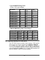
1
ROCKY – 518HV Ver. 4.x
Pentium® w/ VGA Half-Sized
Single Board Computer
@Copyright 1998
All Rights Reserved.
Manual fourth edition April 21,1998
The information in this document is subject to change without prior
notice in order to improve reliability, design and function and does not
represent a commitment on the part of the manufacturer.
In no event will the manufacturer be liable for direct, indirect, special,
incidental, or consequential damages arising out of the use or inability
to use the product or documentation, even if advised of the possibility
of such damages.
This document contains proprietary information protected by copyright.
All rights are reserved. No part of this manual may be reproduced by
any mechanical, electronic, or other means in any form without prior
written permission of the manufacturer.
Trademarks
ROCKY-518HV is registered trademarks of Acquire Inc., IBM PC is a
registered trademark of International Business Machines Corporation.
Intel is a registered trademark of Intel Corporation. AMI is registered
trademarks of American Megatrends, Inc. Other product names
mentioned herein are used for identification purposes only and may be
trademarks and/or registered trademarks of their respective companies.
Contents
1. Introduction .......................................................... 3
1.1
Specifications .............................................................................. 4
1.2
What You Have ........................................................................... 5
2. Installation ............................................................ 6
2.1
ROCKY-518HV............................................................................ 6
2.2
Unpacking ................................................................................... 8
2.3
Setting the CPU of ROCKY-518HV ............................................. 9
2.4
Memory Address for VGA BIOS ................................................. 11
2.5
Watch-Dog Timer ...................................................................... 12
2.6
DiskOnChip™ Flash Disk.......................................................... 12
2.6
Clear CMOS Setup .................................................................... 13
3. Connection ......................................................... 14
3.1
Floppy Disk Drive Connector...................................................... 14
3.2
PCI E-IDE Disk Drive Connector ................................................ 15
3.3
Parallel Port............................................................................... 16
3.4
Serial Ports................................................................................ 16
3.5
Keyboard Connector .................................................................. 17
1
3.6
External Switches and Indicators ............................................... 17
3.7
External Speaker ....................................................................... 18
3.8
PS/2 Mouse 6-Pin Mini-DIN Connector....................................... 18
3.9
USB Port Connector .................................................................. 18
3.10
IrDA Infrared Interface Port ........................................................ 19
3.11
VGA Connector ........................................................................ 19
3.12
External Power Connector.......................................................... 20
3.13
HDD LED Connector.................................................................. 20
3.14
Fan Connector........................................................................... 20
4. AWARD BIOS Setup ......................................... 21
4.1
Getting Start .............................................................................. 21
4.2
Standard CMOS Setup .............................................................. 22
4.3
BIOS Features Setup ................................................................. 24
4.4
Chipset Features Setup.............................................................. 25
4.5
Integrated Peripherals................................................................ 26
4.6
Power Management Setup ......................................................... 27
4.7
PNP/PCI Configuration .............................................................. 28
2
5. E Key Function .................................................. 29
Appendix A. Watch-Dog Timer .............................. 31
2
1
Introduction
Welcome to the ROCKY-518HV Pentium™ w/ VGA Single
Board Computer. The ROCKY-518HV board is an ISA form
factor board, which comes equipped with high performance
Pentium CPU and advanced high performance multi-mode I/O,
designed for the system manufacturers, integrators, or VARs
that want to provide all the performance, reliability, and quality
at a reasonable price.
This board built-in DiskOnChip™ (DOC) Flash Disk for
embedded application. The DOC Flash Disk is 100% compatible
to hard disk. User can use any DOS command without any extra
software utility. The DOC currently is available from 2MB to
72MB. There also have PROMDISK-Chip™ can be used in the
same DOC socket as an alternative solution.
An advanced high performance super AT I/O chip – Winbond
W83877F is used in the ROCKY-518HV board. Both on-chip
UARTs are compatible with the NS16C550. The parallel port and
IDE interface are compatible with IBM PC/AT and XT
architecture's.
In addition, the ROCKY-518HV provides two 72-pin SIMM
sockets for its on-board DRAM. The RAM module accepts 1MB,
2MB, 4MB, 8MB, 16MB, 32MB,and 64MB. So the total on-board
memory can be configured from 2MB to 128MB.
ROCKY-518HV uses the advanced SIS Chipset,5598 which is
100% ISA/PCI compatible chipset with PCI 2.1 standard.
3
1.1 Specifications :
The ROCKY-518HV Pentium w/ VGA Single Board Computer
provides the following specification:
•
CPU : Pentium™ / MMX up to 233/266Mhz, AMD K5/K6 processor,
Cyrix 6x86MX processor
•
Bus : ISA bus and PCI 32-bit local bus, PCI 2.1 standard
•
DMA channels : 7
•
Interrupt levels : 15
•
Chipset : Sis 5598
•
VGA : Built-in the SIS 5598 Chipset
Resolution : 1280 x 1024, 256 color, 75Hz
1024 x 768, 64K color, 75Hz
800 x 600, full color, 90Hz
More information : www.sis.com.tw
•
Real-time clock / calendar : Dallas 12887 or equivalent device. .
•
RAM memory : 2MB to 128MB,EDO and FPM DRAM supported
•
Second Cache memory : 512KB Pipelined Burst SRAM on board
•
Ultra DMA/33 IDE Interface : up to two PCI Enhance IDE hard
drives. The Ultra DMA/33 IDE can handle data transfer up to
33MB/s. The best of all is that is new technology is compatible with
existing ATA-2 IDE specifications. So there is no need to do any
change for customer’s c urrent accessory.
•
Floppy disk drive interface : two 2.88 MB, 1.44MB, 1.2MB, 720KB,
or 360KB floppy disk drives.
•
Two high speed Series ports : NS16C550 compatible UARTs
•
Standard/EPP/ECP Parallel Port
•
IrDA port : Support Serial Infrared(SIR) and Amplitude Shift
Keyed IR(ASKIR) interface.
•
USB port : Support USB ports for future expansion.
4
•
Watch-dog timer : can be set by 1,2,10,20,110 or 220 seconds
period. Reset or NMI was generated when CPU did not periodically
trigger the timer. Your program use hex 043 and 443 to control the
watch-dog and generate a system reset.
•
Flash Disk - DiskOnChip™ or PROMDISK-Chip™ : The Flash
Disk provide 100% compatible with hard disk. The built-in TrueFFS
Transparent Flash Block Management and Space Reclamation will
let customer to use the Flash Disk with DOS command, no need any
extra software utility.
•
Keyboard connector
•
Mouse : PS/2 Mouse Port on-board.
•
Power Consumption : +5V @ 4.6A
( Pentium/MMX-200,16MB EDO RAM)
+12V @ 70mA , -12V@20mA
•
Operating Temperature : 0° ~ 55°C ( CPU needs Cooler)
1.2 What You Have
In addition to this User's Manual, the ROCKY-518HV package
includes the following items:
• ROCKY-518HV Pentium w/ VGA Single Board Computer
•
RS-232/Printer Cable
•
FDD/HDD Cable
•
6-pin Mini-Din to 5-pin Din Keyboard Adapter Cable
If any of these items is missing or damaged, contact the dealer
from whom you purchased the product. Save the shipping
materials and carton in case you want to ship or store the
product in the future.
5
2
Installation
This chapter describes how to install the ROCKY-518HV. At first,
the layout of ROCKY-518HV is shown, and the unpacking
information that you should be careful is described. The
jumpers and switches setting for the ROCKY-518HV's
configuration, such as CPU type selection, system clock setting,
and watch dog timer, are also included.
2.1 ROCKY-518HV Ver. 4.x Layout
< reference next page >
6
7
2.2 Unpacking
Your ROCKY-518HV Single Board Computer contains sensitive
electronic components that can be easily damaged by static
electricity.
In this section, we describe the precautions you should take
while unpacking, as well as during installation. It is very
important that the instructions be followed correctly, to avoid
static damage, and to successfully install the board.
The system board should be done on a grounded anti-static mat.
The operator should be wearing an anti-static wristband,
grounded at the same point as the anti-static mat.
Inspect the cardboard carton for obvious damage. Shipping and
handling may cause damage to your board. Be sure there are no
shipping and handing damages on the board before processing.
After opening the cardboard carton, exact the system board and
place it only on a grounded anti-static surface component side
up.
Again inspect the board for damage. Press down on all the
socketed IC's to make sure that they are properly seated.
Do this only with the board place on a firm flat surface.
Note : DO NOT APPLY POWER TO THE BOARD IF IT HAS
BEEN DAMAGED.
You are now ready to install your ROCKY-518HV Single Board
Computer.
8
2.3 Setting the CPU of ROCKY-518HV
• CPU Clock Setting :
CPU Speed/Clock
50MHz
55MHz
60MHz
66MHz
75MHz
83MHz
JP5
OPEN
OPEN
OPEN
OPEN
CLOSE
CLOSE
JP6
CLOSE
OPEN
OPEN
CLOSE
OPEN
CLOSE
JP7
CLOSE
OPEN
CLOSE
OPEN
OPEN
CLOSE
JP3
1-2
OPEN
CLOSE
CLOSE
OPEN
CLOSE
CLOSE
JP3
3-4
OPEN
OPEN
CLOSE
CLOSE
OPEN
CLOSE
JP3
5-6
OPEN
OPEN
OPEN
OPEN
CLOSE
CLOSE
• CPU to Bus Multiple :
Multiplier
1.5 x or 3.5x
2x
2.5x
3x
4x
4.5 x
CPU Frequency = CPU Clock x Multiplier for example
Pentium 200MHz = 66MHz CPU Clock x 3
• CPU Internal Cache setting :
JP1 : Close Write Through
OPEN Write Back ( default )
• CPU Core Voltage Selection :
Please check the CPU Core Voltage before you install the
CPU. Right now new Intel MMX CPU is dual voltages for core
and I/O, the I/O is 3.3V but the core is 2.8V. This kind of CPU
design will enhance the low power consumption capability. As
for the general Pentium CPU is one voltage for I/O and Core 3.3V,3.4V,or 3.5V
9
• JP1 CPU Core Voltage Setting :
( The JP1 is on the power module,
Pin 7,8 at the left side of HIP6008 IC )
CPU Core
Voltage
3.5V(P54C/CS)
VRE
3.4V(P54C/CS)
STD
3.3V
3.2V
3.1V
3.0V
2.9V
2.8V (P55C)
2.7V
2.6V
2.5V
2.4V
2.3V
2.2V
2.1V
2.0V
JP1
1-2
CLOSE
JP1
3-4
CLOSE
JP1
5-6
CLOSE
JP1
7-8
CLOSE
OPEN
CLOSE
CLOSE
CLOSE
CLOSE
OPEN
CLOSE
OPEN
CLOSE
OPEN
CLOSE
OPEN
CLOSE
OPEN
CLOSE
OPEN
CLOSE
OPEN
OPEN
OPEN
CLOSE
CLOSE
OPEN
OPEN
CLOSE
CLOSE
OPEN
OPEN
CLOSE
CLOSE
OPEN
OPEN
CLOSE
CLOSE
OPEN
OPEN
OPEN
OPEN
CLOSE
CLOSE
CLOSE
CLOSE
OPEN
OPEN
OPEN
OPEN
CLOSE
CLOSE
CLOSE
CLOSE
CLOSE
CLOSE
OPEN
OPEN
OPEN
OPEN
OPEN
OPEN
OPEN
OPEN
• JP4 Dual / Single CPU Voltage setting :
Vcore & VIO
Pentium
(P54C)
Pentium MMX
AMD K6
Cyrix 6x86MX
Dual Voltage
1-3
OPEN
2-4
OPEN
3-5
CLOSE
4-6
CLOSE
CLOSE
CLOSE
OPEN
OPEN
10
• Cyrix 6x86MX PR Rating Table
( Vcore : 2.9V ,dual voltage )
PR Rating
Bus MHz
6x86MX-PR133*
6x86MX-PR150
6x86MX-PR166
6x86MX-PR166
6x86MX-PR166
6x86MX-PR200
6x86MX-PR200
6x86MX-PR200
6x86MX-PR233
6x86MX-PR233
6x86MX-PR266
6x86MX-PR266
55
60
66
55
60
75
66
60
75
66
66
75
CPU Core
MHz
110
120
133
138
150
150
166
180
188
200
233
225
Clock
Multiplier
2x
2x
2x
2.5x
2.5x
2x
2.5x
3x
2.5x
3x
3.5x
3x
• AMD K6 MMX Rating Table ( Dual Voltage )
Product Name
K6-233 Model 6
K6-200 Model 6
K6-166 Model 6
K6-300 Model 7
K6-266 Model 7
K6-233 Model 7
Core Freq
233MHz
200MHz
166MHz
300MHz
266MHz
233MHz
Vcore Bus MHz
3.2V
66
2.9V
66
2.9V
66
2.2V
66
2.2V
66
2.2V
66
Multiplier
3.5 x
3x
2.5 x
4.5 x
4x
3.5 x
2.4 Memory Address for VGA BIOS
The SIS 5598 chipset provides share memory VGA function
which will use the memory address from C0000H to CBFFFH.
It is 16KB more than regular VGA BIOS(from C0000H to
C7FFFH). If customer uses the external LCD or VGA display
card will automatic disable the on board VGA function and
free the C8000H to CBFFFH memory address.
11
2.5 Watch-Dog Timer
The Watch-Dog Timer is enabled by reading port 443H. It should
be triggered before the time-out period ends, otherwise it will
assume the program operation is abnormal and will issue a reset
signal to start again, or activate NMI to CPU. The Watch-Dog
Timer is disable by reading port 043H.
• JP8 : Watch-Dog Active Type Setting
JP8
2-3
1-2
OPEN
DESCRIPTION
RESET WHEN WDT TIME-OUT
ACTIVATE NMI TO CPU WHEN WDT TIME-OUT
DISABLE WDT
• JP12: WDT Time-Out Period
PERIOD
1 sec.
2 sec.
10 sec.
20 sec.
110 sec.
220 sec.
1-2
OPEN
OPEN
OPEN
OPEN
CLOSE
CLOSE
2.6 DiskOnChip™
3-4
OPEN
OPEN
CLOSE
CLOSE
OPEN
OPEN
5-6
CLOSE
CLOSE
OPEN
OPEN
OPEN
OPEN
7-8
OPEN
CLOSE
OPEN
CLOSE
OPEN
CLOSE
Flash Disk
The DiskOnChip™ Flash Disk Chip (DOC) is produced by M
Systems. Because the DOC is 100% compatible to hard disk
and DOS. Customer don‘t need any extra software utility. It is
just “plug and play”, easy and reliable. Right now th e DOC is
available from 2MB to 72MB. The MD-2200-xMB series DOC
will share only 8KB memory address.
• JP11 : DiskOnChip Memory Address Setting
Address
CE000
D6000
DE000
JP11
1-2
3-4
5-6
12
2.7 Clear CMOS Setup
If want to clear the CMOS Setup (for example forgot the
password you should clear the setup and then set the password
again.), you should close the JP17 pin 2-3 about 3 seconds, then
open again. Set back to normal operation mode, close pin 1-2.
• JP10 : Clear CMOS Setup ( Reserve Function )
JP10
OPEN
CLOSE
DESCRIPTION
Normal Operation
Clear CMOS Setup
13
3
Connection
This chapter describes how to connect peripherals, switches and
indicators to the ROCKY-518HV board.
3.1 Floppy Disk Drive Connector
ROCKY-51HV board equipped with a 34-pin daisy-chain driver
connector cable.
• CN3 : FDC CONNECTOR
PIN NO.
1
3
5
7
9
11
13
15
17
19
21
23
25
27
29
31
33
DESCRIPTION
GROUND
GROUND
GROUND
GROUND
GROUND
GROUND
GROUND
GROUND
GROUND
GROUND
GROUND
GROUND
GROUND
GROUND
GROUND
GROUND
GROUND
PIN NO.
2
4
6
8
10
12
14
16
18
20
22
24
26
28
30
32
34
14
DESCRIPTION
REDUCE WRITE
N/C
N/C
INDEX#
MOTOR ENABLE A#
DRIVE SELECT B#
DRIVE SELECT A#
MOTOR ENABLE B#
DIRECTION#
STEP#
WRITE DATA#
WRITE GATE#
TRACK 0#
WRITE PROTECT#
READ DATA#
SIDE 1 SELECT#
DISK CHANGE#
3.2 PCI E-IDE Disk Drive Connector
You can attach four IDE( Integrated Device Electronics) hard
disk drives to the ROCKY-518HV IDE controller.
Please note the IDE support DMA/33 high performance interface.
• CN1 : IDE Interface Connector
PIN NO.
1
3
5
7
9
11
13
15
17
19
21
23
25
27
29
31
33
35
37
39
DESCRIPTION
RESET#
DATA 7
DATA 6
DATA 5
DATA 4
DATA 3
DATA 2
DATA 1
DATA 0
GROUND
IDE DRQ
IOW#
IOR#
IDE CHRDY
IDE DACK
INTERRUPT
SA1
SA0
HDC CS0#
HDD ACTIVE#
PIN NO.
2
4
6
8
10
12
14
16
18
20
22
24
26
28
30
32
34
36
38
40
15
DESCRIPTION
GROUND
DATA 8
DATA 9
DATA 10
DATA 11
DATA 12
DATA 13
DATA 14
DATA 15
N/C
GROUND
GROUND
GROUND
GND
GROUND - DEFAULT
NC
N/C
SA2
HDC CS1#
GROUND
3.3 Parallel Port
This port is usually connected to a printer, The ROCKY-518HV
includes an on-board parallel port, accessed through a 26-pin
flat-cable connector CN9.
• CN9 : Parallel Port Connector
PIN NO.
1
3
5
7
9
11
13
15
17
19
21
23
25
DESCRIPTION
STROBE#
DATA 1
DATA 3
DATA 5
DATA 7
BUSY
PRINTER SELECT
ERROR#
PRINTER SELECT LN#
GROUND
GROUND
GROUND
GROUND
PIN NO.
2
4
6
8
10
12
14
16
18
20
22
24
DESCRIPTION
DATA 0
DATA 2
DATA 4
DATA 6
ACKNOWLEDGE
PAPER EMPTY
AUTO FORM FEED #
INITIALIZE
GROUND
GROUND
GROUND
GROUND
3.4 Serial Ports
The ROCKY-518HV offers two high speed NS16C550
compatible UARTs with Read/Receive 16 byte FIFO serial ports.
• CN16 : Serial Port DB-9 Connector( ACE0 )
PIN NO.
1
2
3
4
5
6
7
8
9
DESCRIPTION
DATA CARRIER DETECT
RECEIVE DATA
TRANSMIT DATA
DATA TERMINAL READY
GROUND
DATA SET READY
REQUEST TO SEND
CLEAR TO SEND
RING INDICATOR
16
(DCD)
(RXD)
(TXD)
(DTR)
(GND)
(DSR)
(RTS)
(CTS)
(RI)
• CN15 : Serial Port 10-pin Header ( ACE1)
Pin No.
1
Description
DCD
2
3
4
5
DSR
RXD
RTS
TXD
Pin No.
6.
7
8
9
10
Description
CTX
DTR
RI
GND
NC
3.5 Keyboard Connector
The ROCKY-518HV provides two keyboard connectors.
• CN17 : 5-pin Header Keyboard Connector
PIN NO.
1
2
3
4
5
DESCRIPTION
KEYBOARD CLOCK
KEYBOARD DATA
N/C
GROUND
+5V
• CN18 : 6-pin Mini-DIN Keyboard Connector
PIN NO.
1
2
3
4
5
6
DESCRIPTION
KEYBOARD DATA
N/C
GROUND
+5V
KEYBOARD CLOCK
N/C
3.6 External Switches and Indicators
There are many external switches and indicators for monitoring
and controlling your CPU board.
• CN4 : KeyLock and Power LED
PIN NO.
1
2
3
4
5
DESCRIPTION
+5V
N/C
Ground
KeyLock Signal
Ground
17
• CN19 : RESET BUTTON
PIN NO.
1
2
DESCRIPTION
EXTERNAL RESET
GROUND
3.7 External Speaker
The ROCKY-518HV has its own buzzer, you also can connect
to the external speaker through the connector JP9.
• JP9 : Speaker Connector
PIN NO.
1
2
DESCRIPTION
+5V
Speaker Signal
3.8 PS/2 Mouse 6-pin Mini-DIN Connector
• CN14 : PS/2 Mouse Connector
PIN NO.
1
2
3
4
5
6
DESCRIPTION
MS DATA
NC
GROUND
+5V
MS CLOCK
NC
3.9 USB Port Connector
The ROCKY-518HV built-in USB ports for the future new I/O bus
expansion.
• CN7 : USB Connector
1
2
3
4
VCC
DATADATA+
GROUND
18
3.10 IrDA Infrared Interface Port
The ROCKY-518HV built-in a IrDA port which support Serial
Infrared(SIR) or Amplitude Shift Keyed IR(ASKIR) interface.
When use the IrDA port have to set SIR or ASKIR model in the
BIOS’s Peripheral Setup’s COM 2. Then the normal RS -232
COM 2 will be disabled.
• CN10 : IrDA connector
PIN NO.
1
2
3
4
5
DESCRIPTION
VCC
NC
IR-RX
Ground
IR-TX
3.11 VGA Connector
The ROCKY-518HV built-in 15-pin VGA connector directly to
your CRT monitor. And additional 10-pin header will help you do
the internal connection to CRT screen in you embedded
application.
• CN13 : 15-pin Female Connector
1
3
5
7
9
11
13
15
RED
BLUE
GROUND
GROUND
NC
NC
HSYNC
DDCCLK
2
4
6
8
10
12
14
GREEN
NC
GROUND
GROUND
GROUND
DDC DAT
VSYNC
• CN12 : 10-pin Header Connector
1
3
5
7
9
RED
GREEN
BLUE
HSYNC
VSYNC
2
4
6
8
10
GROUND
GROUND
GROUND
GROUND
GROUND
19
3.12 External Power Connector
The ROCKY-518HV built-in PC/104 connector. So when use
with the external power connector will create a powerful
embedded system.
• CN11 : External Power Connector
1
3
5
7
+5V
-12V
GROUND
+12V
2
4
6
8
+12V
GROUND
-5V
+5V
3.13 HDD LED Connector
• CN8 : HDD LED connector
PIN NO.
1
2
DESCRIPTION
5V
Ground
3.14 Fan Connector
• CN20 : CPU Fan Connector
PIN NO.
1
2
3
DESCRIPTION
N/C
+12V
Ground
20
4
AWARD BIOS Setup
The ROCKY-518HV uses the AWARD PCI/ISA BIOS for system
configuration. The AWARD BIOS setup program is designed to
provide maximum flexibility in configuring the system by offering
various options which may be selected for end-user
requirements. This chapter is written to assist you in the proper
usage of these features.
4.1 Getting Start
When power on the system, the BIOS will enter the Power-OnSelf-Test routines. These routines will be executed for system
test and initialization and system configuration verification. After
the POST routines are completed, the following message
appears :
" Hit DEL if you want to run SETUP"
To access AWARD PCI/ISA BIOS Setup program, press <Del>
key. The following screen will be displayed at this time.
When choose Load BIOS Defaults will load the minimized
settings for Troubleshooting. The performance should be very
poor when use this setting.
When choose Load Setup Defaults will load optimized defaults
for regular use. Choosing this setting, will modify all applicable
settings.
21
ROM PCI/ISA BIOS (2A5III99)
CMOS SETUP UTILITY
AWARD SOFTWRE, INC.
STANDARD CMOS SETUP
INTEGRATED PERIPHERALS
BIOS FEATURES SETUP
SUPERVISOR PASSWORD
CHIPSET FEATURES SETUP
USER PASSWORD
POWER MANAGEMENT SETUP
IDE HDD AUTO DETECTION
PNP/PCI CONFIGURATION
HDD LOW LEVEL FORMAT
LOAD BIOS DEFAULTS
SAVE & EXIT SETUP
LAD SETUP DEFAULTS
EXIT WITHOUT SAVING
Esc : Quit
↑ ↓ ← → : Select Item
F10 : Save & Exit Setup
(Shift) F2 : Change Color
4.2 Standard CMOS Setup
The Standard CMOS Setup is used for basic hardware system
configuration. The main function is for Date/Time setting and
Floppy/Hard Disk Drive setting. Please refer the following
screen for this setup.
For IDE hard disk drive setup, please check the following
possible
setup procedure,
1. Use the Auto setting for detection during bootup.
2. Use the IDE HDD AUTO DETECTION in the main menu to
automatically enter the drive specifications.
3. Manually enter the specifications by yourself from
the ”User“ option.
22
Halt On (All Errors) : You could choose All Errors, No Errors
All, but Keyboard, All. but Diskette, and All, but Disk/Key
As for some embedded system which don’t need keyboard and
monitor in application, then you could choose No Errors.
ROM PCI/ISA BIOS (2A5III99)
STANDARD CMOS SETUP
AWARD SOFTWRE, INC.
Data (mm : dd : yy) : Sat, Sep 27 1997
Time (hh : mm : ss) : 12 : 42 : 49
HARD DISKS
Primary Master
Primary Slave
TYPE SIZE CYLS HEAD PRECOMP LANDZ SECTOR
: Auto
: Auto
0
0
0
0
0
0
Drive A : 1.44M, 3.5 in.
Drive B : None
Video
: EGA/VGA
Halt on : All Errors
0
0
0 NORMAL
0 NORMAL
Base Memory :
Extended Memory :
Other Memory :
0K
0K
512K
Total Memory :
512K
Esc : Quit
↑ ↓ ← → : Select Item
F1
(Shift) F2 :
: Help
0
0
23
Change Color
MODE
PU / PD / + / - : Modify
4.3 BIOS Features Setup
This BIOS Features Setup is designed for customer‘s tuning best
performance of the ROCKY-518HV board. As for normal
operation customers don‘t have to cha nge any default setting.
The default setting is pre-setted for most reliable operation.
ROM PCI/ISA BIOS (2A5III99)
BIOS FEATURES SETUP
AWARD SOFTWRE, INC.
Virus Warning
CPU Internal Cache
External Cache
Quick Power On Self Test
Boot Sequence
Swap Floppy Seek
Boot Up Floppy Seek
Boot Up NumLock Status
Boot Up System Speed
Gate A20 Option
Memory Parity Check
Typematic Rate Setting
Typematic Rate (Chars/Sec)
Typematic Rate (Msec)
Security Option
PCI / VGA Palette Snoop
OS Select For DRAM > 64MB
:
:
:
:
:
:
:
:
:
:
:
:
:
:
:
:
:
Enabled
Enabled
Enabled
Disabled
A,C,SCSI
Disabled
Disabled
On
High
Fash
Disabled
Disabled
6
250
Setup
Disabled
Non-OS2
Video
C8000
CC000
D0000
D4000
D8000
DC000
ESC :
F1 :
F5 :
F2 :
F6 :
F7 :
Bios
- CBFFF
- CFFFF
- D3FFF
- D7FFF
- DBFFF
- DFFFF
Shadow
Shadow
Shadow
Shadow
Shadow
Shadow
Shadow
:
:
:
:
:
:
:
Enabled
Disabled
Disabled
Disabled
Disabled
Disabled
Disabled
Quit
↑ ↓ ← → : Select Item
Help
PU / PD / + / - : Modify
Old Values
(Shift)
Color
Load BIOS Defaults
Load Setup Defaults
BootUp Sequence :
You could set the sequence of A:, C:, and CDROM.
Video BIOS Shadow C000,32K:
Enable - Will increase the video speed.
Shadow C8000-CFFFF,D0000-D7FFF,& D8000-DFFFF :
When the installed add-on card‘s ROM address is as
above address, you could enable the shadow to get higher
operation performance. When you enable the shadow
function, it will also reduce the memory available by between
640KB and 1024KB.
24
4.4 Chipset Features Setup
This setup functions are almost working for ChipSet (SIS 5598).
These options are used to change the ChipSet‘s registers.
Please carefully change any default setting ,otherwise the
system could be running un-stable.
Auto Configuration : Enable or Disable
When use the 60nS general type DRAM, please enable the
setting to get the optimal timings.
VGA Shared Memory : 0.5MB to 4MB
The SIS5598 provides UMA architect which can share the on
board memory from 0.5MB to 4MB. The default setting is 2MB.
Memory Hole at 15M-16M : Enable or Disable
This setting reserve 15MB to 16MB memory address space for
ISA expansion cards that specifically require this setting.
Memory from 15MB and up will be unavailable to the system
because expansion cards can only access memory up to 16MB.
ROM PCI/ISA BIOS (2A5III99)
CHIPSET FEATURES SETUP
AWARD SOFTWRE, INC.
Auto Configuration
: Enabled
L2
(WB)
Tag Bit Length
:
SRAM Back–to–Back
:
NA# Enable
:
Starting Point of Paging
:
Refresh Cycle Time (us)
:
RAS Pulse Width Refresh
:
RAS Precharge Time
:
RAS to CAS Delay
:
CAS# Pulse Width (FP)
:
CAS# Pulse Width (EDO)
:
RAMW# Assertion Timing
:
CAS# Precharge Time (FP)
:
CAS# Precharge Time (EDO) :
SDRAM WR Retire Rate
:
SDRAM Wait State Control
:
Enhanced Memory Write
:
Read Prefetch Memory RD
:
CUP to PCI Post Write
:
7bits
Enabled
Disabled
1T
15.6
4T
2T
2T
2T
2T
3T
1T
1T
X-2-2-2
1WS
Disabled
Enabled
4T
25
CPU to PCI Burst Mem. WR: Disabled
ISA Bus Clock Frequency : PCICLK/4
System BIOS Cacheable : Enabled
Video
BIOS Cacheable : Enabled
Memory Hole at 15M-16M : Disabled
VGA Shared Memory Size: 2 MB
VGA Memory Clock (MHz): 40
Linear Mode SRAM Support : Disabled
ESC
F1
F5
F6
F7
:
:
:
:
:
Quit
↑ ↓ ← → : Select Item
Help
PU / PD / + / - : Modify
Old Values (Shift) F2 : Color
Load BIOS Defaults
Load Setup Defaults
4.5 Integrated Peripherals
This setup is almost working for Multi-I/O Chip(W83877F ).
These options are used to change the ChipSet‘s registers.
Please carefully change any default setting to meet your
application need perfectly. The only special concern is Onboard
Serial Port2. If you are using the IrDA port, you have to set this
port accordingly.
ROM PCI/ISA BIOS (2A5III99)
INTEGRATED PERIPHERALS
AWARD SOFTWRE, INC.
Internal PCI/IDE
IDE Primary Master
IDE Primary Slave
IDE
IDE
IDE
: Primary
: Auto
: Auto
PIO
PIO
Burst
Mode
: Disabled
Data Port Post Write : Disabled
HDD Block Mode
: Disabled
Onboard FDD Controller
Onboard Serial Port 1
Onboard Serial Port 2
UART
2
Mode
:
:
:
:
Onboard
Onboard
: 378/IRQ7
: EPP/SPP
Parallel
Parallel
Port
Mode
Parallel Port EPP Type
:
Enabled
3F8/IRQ4
5F8/IRQ3
Standard
EPP1.9
PS/2
Mouse
function
USB Controller
USB Keyboard Support
: Enabled
: Enabled
: Disabled
Month Alarm
Day of Month Alarm
W eek Alarm
: NA
: 0
*** SUN MON TUE WED THU FRI SAT ***
Off Off Off Off Off Off Off
Time (hh : mm : ss)
Alarm : 0: 0: 0
ESC
F1
F5
F6
F7
26
:
:
:
:
:
Quit
Help
Old Values
Load BIOS
Load Setup
↑ ↓ ← → : Select Item
PU / PD / + / - : Modify
(Shift) F2 : Color
Defaults
Defaults
4.6 Power Management Setup
Power Management Setup help user handles the ROCKY518HV board‘s “green” function. The features could shut down
the video display and hard disk to save energy for example. The
power management setup screen is as following,
Power Management : Disable, Max Saving, Min Saving,
or User Defined
Max Saving puts the system into power saving mode after a
brief inactivity period. Min Saving is almost the same as Max
Saving except that the inactivity period is longer. User Defined
allows you to set power saving options according to your
requirement.
Note : Advanced Power Management(APM) have to be
installed to keep the system time updated when the computer
enters suspend mode activated by the Power Management.
Under DOS environment, you need to add
DEVICE=C:\DOS\POWER.EXE in your CONFIG.SYS
Under Windows 3.x and Windows 95,you have to install Windows
with APM feature. A battery and power cord icon labeled “Power”
Will appear in the “Control Panel”
ROM PCI/ISA BIOS (2A5III99)
CHIPSET FEATURES SETUP
AWARD SOFTWRE, INC.
Power Management
PM Control By APM
Video Off Option
Video Off Method
Switch Function
Doze Speed ( div by )
Stdby Speed ( div by )
MODEM Use IRQ
Hot Key Power Off
:
:
:
:
:
:
:
:
:
Max Saving
Yes
Always On
Blank Screen
Disabled
1
1
NA
Enabled
** PM Timers **
HDD Off After
Doze Mode
Standby Mode
Suspend Mode
: Disable
: 20 Sec
: 20 Sec
: 20 Sec
** PM Events **
COM Ports Activity
LPT
Ports Activity
HDD Ports Activity
: Disable
: Disable
: Disable
VGA Activity
IRQ3
( COM 2 )
IRQ4
( COM 1 )
IRQ5
( LPT 2 )
IRQ6
( Floppy Disk )
IRQ7
( LPT 1 )
IRQ8
( RTC Alarm )
IRQ9
( IRQ2 Redir )
IRQ10
( Reserved )
IRQ11
( Reserved )
IRQ12
( PS/2 Mouse )
IRQ13
( Coprocessor )
IRQ14
( Hard Disk )
IRQ15 ( Reserved )
ESC
F1
F5
F6
F7
27
:
:
:
:
:
Quit
Help
Old Values
Load BIOS
Load Setup
:
:
:
:
:
:
:
:
:
:
:
:
:
Disabled
Enabled
Enabled
Enabled
Enabled
Enabled
Enabled
Enabled
Enabled
Enabled
Enabled
Enabled
Enabled
: Enabled
↑ ↓ ← → : Select Item
PU / PD / + / - : Modify
(Shift) F2 : Color
Defaults
Defaults
4.7 PNP/PCI Configuration
The PNP/PCI Configuration help user handles the ROCKY518HV board‘s “PCI” function. All PCI bus slots on the system
use INTA#, thus all installed PCI slots must be set to this value.
The ROCKY-518HV only have ISA interface but the on board
IDE is PCI interface..
PNP OS Installed : Yes or No
When PNP OS is installed, interrupts may be reassigned by the
OS when the setting is Yes. When a non-PNP OS is installed or
to prevent reassigning of interrupt settings, select setting to No.
ROM PCI/ISA BIOS (2A5III99)
PNP/PCI CONFIGURATION
AWARD SOFTWRE, INC.
PNP OS Installed
:
Resources Controlled By :
Reset Configuration Data :
No
Auto
Disabled
PCI IRQ Actived By
PCI IDE 2nd Channel
PCI IDE IRQ Map To
Primary
IDE INT#
Secondary IDE INT#
ESC
F1
F5
F6
F7
28
:
:
:
:
:
Quit
Help
Old Values
Load BIOS
Load Setup
:
:
:
:
:
Edge
Disabled
PCI-AUTO
A
A
↑ ↓ ← → : Select Item
PU / PD / + / - : Modify
(Shift) F2 : Color
Defaults
Defaults
5
2
E Key™ Function
2
The ROCKY-518HV provides an outstanding E KEY™ function
2
for system integrator. Based on the E KEY™ you could free to
store the ID Code, Pass Word, or Critical Data in the 1Kbit
EEPROM. Because the EEPROM is nonvolatile memory, you
don’t have to worry the losing of the very important data.
2
Basically the E KEY™ is based on a 1Kbit EEPROM which is
configured to 64 words(from 0 to 63). You could access(read or
write) each word at any time.
2
When you start to use the E KEY™ you should have the ut
ility in
the package. The software utility will include four files as follows,
README.DOC
E2KEY.OBJ
EKEYDEMO.C
EKEYDEMO.EXE.
The E2KEY.OBJ provides two library function for user to
2
integrate their application with E KEY™ function. These brary
li
(read_e2key and write_e2key) are written and compiled in C
format. Please check the following statement, then you will know
how to implement it easily.
unsigned int read_e2key (unsigned int address)
2
/* This function will return the E KEY™ s’ data at address. The
address range is from 0 to 63. Return data is one word,16 bits */
29
void write_e2key (unsigned int address, unsigned data)
2
/* This function will write the given data to E KEY™ at address.
The address range is from 0 to 63. The data value is from 0 to
0xffff. */
To easy start to use the function, please refer the include
EKEYDEMO.C code at first.
2
Please note the E KEY™ function is based on the working of
parallel port. So you should enable the ROCKY-518HV’s parallel
port, otherwise will be not working.
30
Appendix A. Watch-Dog Timer
The Watch-Dog Timer is provided to ensure that standalone
systems can always recover from catastrophic conditions that
caused the CPU to crash. This condition may have occurred by
external EMI or a software bug. When the CPU stops working
correctly, hardware on the board will either perform a hardware
reset (cold boot) or a non-maskable interrupt (NMI) to bring the
system back to a known state.
The Watch-Dog Timer is controlled by two I/O ports.
443
(hex)
043
(hex)
Read
Read
Enable the refresh the Watch-Dog
Timer.
Disable the Watch-Dog Timer.
To enable the Watch-Dog Timer, a read from I/O port 443H
must be performed. This will enable and activate the countdown
timer which will eventually time out and either reset the CPU or
cause an NMI depending on the setting of JP8. To ensure that
this reset condition does not occur, the Watch-Dog Timer must
be periodically refreshed by reading the same I/O port 433H.
This must be done within the time out period that is selected by
jumper group JP12.
A tolerance of at least 30% must be maintained to avoid
unknown routines within the operating system (DOS), such as
disk I/O that can be very time consuming. Therefore if the time
out period has been set to 10 seconds, the I/O port 443H must
be read within 7 seconds.
Note: when exiting a program it is necessary to disable the WatchDog Timer, otherwise the system will reset.
31