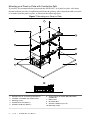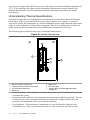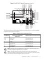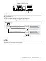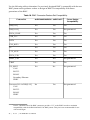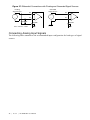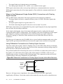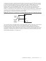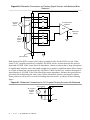
1
USER MANUAL
NI sbRIO-9627
Single-Board RIO OEM Devices
This document describes the features of the NI sbRIO-9627 and contains information about
operating the device.
Figure 1. NI sbRIO-9627 Block Diagram
SDIO
Connector
sbRIO-9627
Zynq-7020
512 MB
NAND Flash
Battery
512 MB
DDR3
Real-time
Clock
Processor
USB
PHY
User
LED
USB
PHY
ENET 0
Connector
GIGE 0
PHY
CAN
XCVR
Serial Port 1
Connector
RS-232
XCVR
Serial Port 2
Connector
RS-232
XCVR
Serial Port 3
Connector
RS-485
XCVR
MIO
Connector
CAN Port 0
Connector
FPGA
LED
Temp
Sensors
GIGE 1
PHY
x4 Digital I/O
(3.3 V, 5V Tolerant)
Pre-Magnetic MDI Pairs
x96 Digital I/O (3.3 V)
x2 C Series Module Interface
40 MHz
Oscillator
3.3 V_Aux
5V
FPGA_VIO
FPGA
Optional System
Power
x16 MUX
Analog Input
x4
Analog Output
USB Host/Device
RMC Connector
USB
Connector
VBAT
Reset In/Out
On-board
Power
Supply
Power
Selection
Power
Connector
Status
LED
Contents
Mechanical Considerations....................................................................................................... 3
Dimensions........................................................................................................................4
Maximum Component Heights......................................................................................... 6
Mounting........................................................................................................................... 7
Managing Thermal Conditions........................................................................................11
Validating the System......................................................................................................13
Shock and Vibration........................................................................................................18
Ports and Connectors.............................................................................................................. 18
Connector Descriptions...................................................................................................19
Power Connector.............................................................................................................21
RJ-45 Gigabit Ethernet Port............................................................................................ 21
USB Host Ports............................................................................................................... 22
SD Connector.................................................................................................................. 23
RS-232 Serial Ports......................................................................................................... 23
RS-485 Serial Port.......................................................................................................... 24
CAN Port.........................................................................................................................25
MIO Port......................................................................................................................... 26
RESET Button.........................................................................................................................26
System Reset................................................................................................................... 27
LEDs....................................................................................................................................... 27
POWER LED Indicators................................................................................................. 28
STATUS LED Indicators.................................................................................................28
User LEDs.......................................................................................................................29
Ethernet LED Indicators................................................................................................. 30
Real-Time Clock (RTC) Battery............................................................................................. 30
Internal Real-Time Clock (RTC).............................................................................................31
RIO Mezzanine Card Connector.............................................................................................31
RMC Connector Pins...................................................................................................... 32
RMC Connector Pin Listing by Location....................................................................... 36
RMC Connector Power Requirements............................................................................39
RMC Connector Electrical Characteristics..................................................................... 39
VIN_Filtered................................................................................................................... 40
RMC VBAT.................................................................................................................... 40
USB Support................................................................................................................... 40
RMC Ethernet Support....................................................................................................41
C Series DIO................................................................................................................... 41
RMC RST#..................................................................................................................... 42
SYS RST#....................................................................................................................... 42
FPGA_CONF..................................................................................................................42
User-Defined FPGA Signals........................................................................................... 42
Integrated 3.3 V Digital I/O.................................................................................................... 44
Integrated Analog Input.......................................................................................................... 45
Analog Input Range........................................................................................................ 45
Integrated Analog Output........................................................................................................53
Analog Output Startup and Initialization........................................................................ 53
2 |
ni.com
|
NI sbRIO-9627 User Manual
Power Requirements............................................................................................................... 53
Wiring the Power Supply Connector.............................................................................. 53
Powering On the NI sbRIO Device.................................................................................54
Calculating the Power Requirement............................................................................... 54
Configuring the sbRIO-9627.................................................................................................. 56
Connecting the sbRIO-9627 to the Host Computer........................................................ 56
Configuring Startup Options........................................................................................... 57
Configuring FPGA Startup App..................................................................................... 59
Connecting CAN Networks.................................................................................................... 59
CAN Bus Topology and Termination............................................................................. 59
Cable Specifications........................................................................................................60
Termination Resistors......................................................................................................60
Cable Lengths................................................................................................................. 61
Number of CAN Nodes...................................................................................................61
File System..............................................................................................................................61
Worldwide Support and Services............................................................................................ 61
Mechanical Considerations
Proper mechanical design is critical for rugged environments in which the NI sbRIO device
may be subjected to extreme temperatures, shock, vibration, and other factors. In particular,
pay special attention to thermal performance to ensure that your application meets the
NI sbRIO device operating requirements.
NI sbRIO-9627 User Manual |
© National Instruments
|
3
Dimensions
The following figures specify dimensions for the sbRIO-9627.
11.19 (0.440)
10.76 (0.423)
10.30 (0.405)
43.95 (1.730)
38.24 (1.505)
31.84 (1.253)
65.01 (2.559)
64.38 (2.534)
142.43 (5.607)
Figure 2. Primary-Side Dimensions in mm (in.)
CPU/FPGA
DDR Memory
NAND Flash
77.33 (3.044)
70.39 (2.771)
66.73 (2.627)
62.85 (2.474)
51.82 (2.040)
50.17 (1.975)
44.36 (1.746)
44.38 (1.747)
84.51 (3.327)
Pin 1
Pin 2
Pin 2
Pin 1
Pin 2
Pin 1
17.12 (0.674)
ENET PHY
USB PHY
Pin 2
CPLD
18.13 (0.714)
17.17 (0.676)
Pin 1
0.00 (0.000)
0.64
(0.025)
1. Back of Front Panel
4 | ni.com
|
NI sbRIO-9627 User Manual
0.0 (0.000)
20.63 (0.812)
Pin 1
69.47 (2.735)
1
139.07 (5.475)
149.89 (5.900)
Pin 2
76.84 (3.025)
40.03 (1.576)
3.20 (0.126)
150.47 (5.924)
Figure 3. Secondary-Side Dimensions in mm (in.)
Pin 1
102.87 (4.050)
98.40 (3.874)
96.75 (3.809)
1 6x Ø 3.18 (0.125)
26.67 (1.050)
153.67 (6.050)
0.0 (0.00)
0.0 (0.00)
1. Holes and Keepouts Sized for M3 Standoff (4.5 mm Hex) or 4-40 Standoff (3/16-in. Hex)
10.16 (0.400)
7.62 (0.300)
5.08 (0.200)
2.54 (0.100)
19.50 (0.768)
33.99 (1.338)
57.52 (2.265)
49.73 (1.958)
76.82 (3.025)
70.02 (2.757)
103.02 (4.056)
95.21 (3.748)
89.81 (3.536)
127.47 (5.018)
Figure 4. Front Dimensions in mm (in.)
1
8.76 (0.345)
6.32 (0.249)
4.66 (0.183)
3.66 (0.144)
2.56 (0.101)
15.64 (0.616)
6.16 (0.242)
05.34 (0.210)
2.16 (0.085)
0.00 (0.000)
0.0 (0.00)
18.16
(0.715)
1. Minimum Clearance for Latch on Mating Power Connector
Tip For two-dimensional drawings and three-dimensional models of the
sbRIO-9627, visit ni.com/dimensions and search by model number.
NI sbRIO-9627 User Manual |
© National Instruments
|
5
Maximum Component Heights
The primary side of the sbRIO-9627 is the top side of the PCB populated with the power and
Ethernet connectors. The secondary side is the bottom side of the PCB populated with the
RMC connector. The following figures show the maximum component heights for the
different regions of the primary and secondary sides.
Note In addition to the maximum component heights, you must also observe
minimum keepaway distances for adjacent PCBs and surfaces.
Figure 5. Maximum Component Height of Primary Side
96.52 mm (3.800 in.)
Max Component Height =
9.53 mm (0.375 in.)
Min Adjacent Surface Height =
9.53 mm (0.375 in.)
Max Component Height =
7.11 mm (0.280 in.)
Min Adjacent Surface Height =
8.89 mm (0.350 in.)
31.75 mm
(1.250 in.)
Max Component Height =
17.27 mm (0.680 in.)
Min Adjacent Surface Height =
19.05 mm (0.750 in.)
6 | ni.com
|
NI sbRIO-9627 User Manual
Figure 6. Maximum Component Height of Secondary Side
10.16 mm
(0.400 in.)
60.95 mm
(2.400 in.)
Max Component Height =
7.62 mm (0.300 in.)
Min Adjacent Surface Height =
7.62 mm (0.300 in.)
11.43 mm
(0.450 in.)
Max Component Height =
6.15 mm (0.242 in.)
Min Adjacent Surface Height =
7.62 mm (0.300 in.)
Mounting
You can mount the NI sbRIO device in a variety of ways in order to maximize system
performance. Some mounting methods might require custom fasteners or unique assembly
techniques to maintain required connector stack heights and enable improved thermal and
structural design for rugged environments.
Mounting Direction Options
The sbRIO-9627, Thermal Kit for NI sbRIO-9607/9627/9637 (153901-02), and certain RMC
accessories are designed to allow traditional M-F standoff threads to pass through and stack in
either direction. The following figures show possible mounting configurations and associated
fastener types.
NI sbRIO-9627 User Manual |
© National Instruments
|
7
Mounting on a Panel or Plate with Conduction Path
If possible, NI recommends that you mount the sbRIO-9627 on a panel or plate, such that a
thermal solution provides a conduction path from the primary side components and is secured
to or made from the panel or plate, as shown in the following figure.
Figure 7. Mounting on a Panel or Plate
1
3
7
4
8
9
5
10
6
2
1.
2.
3.
4.
5.
Exploded view of all mounting components
Complete assembled and mounted view
Mounting screws
Standoff, 9.65 mm (0.38 in.)
Standoff, 16.00 mm (0.63 in.)
8 | ni.com
|
NI sbRIO-9627 User Manual
6. Thermal Kit for NI sbRIO-9607/9627/9637
(153901-02)
7. RMC board
8. NI sbRIO-9627
9. Standoff, 18.00 mm (0.71 in.)
10. Mounting surface
Mounting on a Panel or Plate with Convection Path
Alternatively, the thermal solution can be used for convection to natural or forced air flow or
used in conjunction with a heat sink optimized for the environment.
NI sbRIO-9627 User Manual |
© National Instruments
|
9
Figure 8. Mounting on a Panel or Plate
1
7
3
8
4
9
5
10
6
11
2
1.
2.
3.
4.
Exploded view of all mounting components
Complete assembled and mounted view
Heatsink
Thermal Kit for NI sbRIO-9607/9627/9637
(153901-02)
5. NI sbRIO-9627
6. RMC board
10 |
ni.com
|
NI sbRIO-9627 User Manual
7. Mounting screws
8. Standoff, 16.00 mm (0.63 in.)
9. Standoff, 9.65 mm (0.38 in.)
10. Standoff
11. Mounting surface
Chassis Grounding Connections
The sbRIO-9627 provides a multi-function bracket that can be used with the supplied 4-40
grounding screw for directly attaching ground connections or for attaching to and grounding a
front panel as shown in the following figure.
Figure 9. sbRIO-9627 Chassis Grounding Screw
1
1. Chassis Grounding Screw
The front I/O connector shields, chassis ground bracket, and mounting holes near the front I/O
are connected together internally to form chassis ground. Chassis ground is capacitively
coupled to digital ground near each of the IO connectors. For the best possible ESD protection,
connect chassis ground at the mounting holes or the chassis ground bracket to a lowinductance earth ground.
When connecting the NI sbRIO device to external devices, ensure that stray ground currents
are not using the device as a return path. Significant stray currents traversing through the
NI sbRIO device can result in device failure.
To verify correct grounding of the NI sbRIO device, make sure the current flowing into the
power connector equals the current flowing out of the power connector. These currents should
be measured with a current probe after final assembly of the end system. Investigate and
remove any current differences.
Managing Thermal Conditions
Due to the small size of the sbRIO-9627, it is very important to appropriately dissipate the heat
generated during operation. You must plan for the thermal conditions of your application
throughout development and validation. This section provides design recommendations and
validation tools and methods for maximizing the thermal performance of the system.
Designing a Suitable Enclosure
NI sbRIO devices operate as components in a higher-level system and may require an
enclosure to protect the internal circuit card assembles and dissipate heat. For the sbRIO-9627,
the system integrator is responsible for designing an enclosure that meets the thermal
requirements of your specific application.
NI sbRIO devices integrated into an enclosure or system with proper thermal dissipation can
be deployed in high- and low-temperature environments. However, the 85 °C local ambient
operating temperature rating of the sbRIO-9627 does not mean that the external temperature of
the natural convection environment such as a room or larger enclosure can be 85 °C. In this
NI sbRIO-9627 User Manual |
© National Instruments
|
11
way, properly designed NI sbRIO devices may still require an external ambient temperature of
70 °C or less and may still require specific mounting requirements to ensure that the local
ambient and thermally-relevant component maximum operating temperatures are within
specification.
Understanding Thermal Specifications
A deployed system has several temperature measurement locations that indicate the thermal
performance of the system and the devices the system contains. For example, in a natural
convection system, the temperature of a critical component will be higher than the temperature
of the air in the immediate vicinity of the component. This local air temperature will also be
higher inside an enclosure than in the room ambient that surrounds the enclosure.
The following figure identifies these types of ambient temperatures.
Figure 10. Ambient Temperatures
1
2
3
7
5
4
6
1.
2.
3.
4.
•
•
•
12 |
External ambient temperature
Internal/enclosure ambient temperature
Local ambient temperature
Enclosure
5. RMC board
6. NI sbRIO-9627
7. Thermal Kit for NI sbRIO-9607/9627/9637
(153901-02)
External ambient—The maximum air temperature of the room or installation location that
surrounds the system.
Internal/enclosure ambient—The maximum air temperature inside the enclosure. This can
be measured at various locations within the enclosure and is highly influenced by the
proximity and dissipation of devices inside the enclosure.
Local ambient—The maximum air temperature as specified directly adjacent to the
NI sbRIO device. This is measured on all sides of a device that has exposed circuitry.
ni.com
|
NI sbRIO-9627 User Manual
Because the system integrator may use any number of enclosure sizes, materials, thermal
solutions, and room conditions when designing an enclosure for a specific application,
NI sbRIO devices are specified in a manner that removes most of these external variables.
Therefore, the sbRIO-9627 thermal performance is not determined by measuring the external
ambient or internal/enclosure ambient temperatures, but by measuring the local ambient and
specific component temperatures. NI provides digitally reported temperatures to help you
accurately measure these critical temperatures.
Validating the System
NI recommends that you use a validation system for an extended period of time in a test
environment with the same thermal, environmental, and functional utilization characteristics as
the target deployment environment. You are responsible for final validation of your
application.
Validating Temperature Measurements Digitally
To meet the thermal specifications of the sbRIO-9627, you must satisfy the requirements of
either the digital or analog thermal validation approach as described in the NI sbRIO-9627
Specifications on ni.com/manuals. The sbRIO-9627 includes three onboard temperaturemonitoring sensors to simplify validation of a thermal solution. The sensors provide an
indication of thermal performance and are used to validate the system digitally.
NI sbRIO-9627 User Manual |
© National Instruments
|
13
Figure 11. Onboard Temperature-Monitoring Sensors
2
1
3
1. CPU/FPGA sensor
2. Primary System sensor
3. Secondary System sensor
•
•
•
CPU/FPGA sensor—Digitally reports the die junction temperature of the Xilinx Zynq
SoC.
Primary System sensor—Digitally reports the temperature on the Xilinx Zynq SoC side
of the circuit card assembly. This value is a conservative approximation of the local
ambient temperature on that side of the circuit card assembly.
Secondary System sensor—Digitally reports the temperature on the SEARAY side of the
circuit card assembly. This value is a conservative approximation of the local ambient
temperature on that side of the circuit card assembly.
In addition to being useful for system validation, digitally reported temperatures also provide
feedback about system health and can be used as triggers or set points.
NI recommends that you monitor the digitally reported temperatures on deployed systems,
especially if the temperatures approach the maximum thermal specifications during system
validation testing. Monitoring allows individual systems to identify adverse thermal changes
caused by differences in environmental, operating, or process conditions.
For more information about how to access and use the digitally reported temperature sensor
measurements, visit ni.com/info and enter the Info Code sbriosensors.
14 |
ni.com
|
NI sbRIO-9627 User Manual
Managing Power and Feature Utilization
An NI sbRIO device that heavily utilizes all of its performance and features consumes and
dissipates substantially more power than an idle device.
Consider the following options for reducing the die junction temperature.
•
Design for additional thermal cooling that can appropriately dissipate power
•
Reduce device feature utilization
Note Your final validation must consider software and hardware utilization that is
representative of the final deployment conditions.
Note Refer to the Power Requirements section of the NI sbRIO-9627
Specifications on ni.com/manuals for specifications that approximate the maximum
power requirement for each input rail on the sbRIO device with worst-case silicon
manufacturing process and maximum junction temperatures. For a more accurate
estimate of the power consumption for a specific application, NI recommends that
you directly measure the power the sbRIO device consumes when running your
application in an environment that is representative of the intended use case.
Mounting Recommendations for Maximizing Thermal
Performance
Thermal performance of the NI sbRIO device can be maximized by implementing the
following recommendations.
•
Directly mount a thermal solution such as the Thermal Kit for NI sbRIO-9607/9627/9637
(153901-02) to a thermally conductive surface such as a metal enclosure wall or plate, as
shown in the Mounting on a Panel or Plate with Conduction Path section. An interface
material such as thermal grease should be used to maximize the heat transfer from the
heat spreader to the enclosure or plate.
•
•
If design limitations prevent this solution, you can alternatively attach a heat sink or other
thermal solution as shown in the Mounting on a Panel or Plate with Convection Path
section. This solution takes advantage of natural convection or forced cooling provided
by a fan.
Mount the NI sbRIO device vertically with respect to gravity to take advantage of natural
convection cooling.
Mount the NI sbRIO device below and away from other heat-dissipating components.
Note Placing the NI sbRIO device within a system or enclosure will also influence
thermal performance.
The following figure shows good, better, and best thermal mounting solutions for the
sbRIO-9627.
NI sbRIO-9627 User Manual |
© National Instruments
|
15
Figure 12. Thermal Mounting Solutions Comparison
1
2
3
1. Good—Horizontal mounting with no additional thermal provisions
2. Better—Vertical mounting with an attached heat sink
3. Best—Vertical mounting directly to a thermally-conductive wall or plate
Designing A Thermal Solution
If the Thermal Kit for NI sbRIO-9607/9627/9637 (153901-02) does not satisfy your design
requirements, NI recommends replicating the features of the heat spreader into your own
thermal solution. Use the pedestal dimensions shown in the following figure and a Bergquist
GPVOUS-0.060 thermal gap pad with a fastener assembly rate of 4.23 mm/s (10 in./min.) to
prevent damage to the critical components during assembly. NI recommends that you replicate
each of the pedestals and not just the pedestal for the CPU/FPGA.
16 |
ni.com
|
NI sbRIO-9627 User Manual
A
H
28.69 (1.130)
18.25 (0.718)
15.84 (0.624)
4.71 (0.185)
4.10 (0.162)
B
67.88 (2.672)
68.51 (2.697)
61.46 (2.420)
60.83 (2.395)
47.76 (1.880)
Figure 13. sbRIO-9627 Pedestal Dimensions in mm (in.)
G
F
81.89 (3.224)
76.26 (3.002)
73.90 (2.909)
72.75 (2.864)
67.40 (2.654)
57.19 (2.252)
55.35 (2.179)
48.30 (2.901)
46.94 (2.848)
41.81 (2.646)
58.27 (2.294)
54.22 (2.135)
46.10 (1.815)
46.93 (1.847)
41.79 (1.645)
46.51 (1.831)
41.38 (1.629)
34.39 (1.354)
29.25 (1.152)
C
14.82 (0.583)
6.69 (0.263)
0.0 (0.000)
E
0.0 (0.000)
D
The following table provides the pedestal height from board surface for each corresponding
component shown in the previous figure.
Table 1. Pedestal Height from Board Surface
Designation
Pedestal Corresponding
Component
Pedestal Height from Board Surface
A, B
ENET PHY
2.05 mm (0.081 in.)
C, D
USB PHY
2.00 mm (0.079 in.)
E
CPLD
2.20 mm (0.087 in.)
F
NAND Flash
2.16 mm (0.085 in.)
G
DDR Memory
2.32 mm (0.091 in.)
H
CPU/FPGA
2.51 mm (0.099 in.)
Note Pedestals of the same dimensions are allowed to violate the primary side
maximum component height keepaway restrictions.
Note Gap-filling thermal interface materials between the components and
pedestals confined to within the indicated region are allowed to violate the primary
side maximum component height keepaway restrictions.
NI sbRIO-9627 User Manual |
© National Instruments
|
17
Note Pedestals of the same dimensions are allowed to have 0.5 mm (0.02 in.)
rounds and 2° draft angles.
Additional Resources for Managing Thermal Conditions
Visit ni.com/info and enter the Info Code sbriocooling for the following additional
information to help you manage thermal conditions:
•
Examples regarding the effect of the design factors discussed in this chapter
•
Case study examples to help you estimate the achievable external ambient temperature
for a representative system
Shock and Vibration
The mounting method you use, components you select, and assembly techniques you use
influence the ability of the system to resist fretting corrosion and other damage caused by
exposure to shock and vibration. Consider the following factors when designing your
sbRIO-9627 system to account for shock and vibration:
•
In general, shorter SEARAY stack heights perform better than taller stack heights.
•
Directly mounting the thermal solution to a rigid surface provides the best performance.
If this method is not feasible for your design, minimize the amount of extra mass that
only the sbRIO-9627 supports, such as a heat sink or other thermal solution, that is
fastened to the four standoffs. If you require substantial thermal solutions, provide
additional structural support.
•
NI recommends that you use connectors that provide the following benefits:
–
Positive locking
–
Provisions for strain relief
–
Substantial gold plating on pins
•
The sbRIO-9627 has been tested to industry specifications for rugged environments.
•
NI offers a variety of cable assemblies and other connectivity accessories to complete
your system design. Typically, these accessories include the best available designs,
materials, and plating to maximize performance and longevity in rugged environments.
Ports and Connectors
The sbRIO-9627 provides the following ports and connectors.
18 |
ni.com
|
NI sbRIO-9627 User Manual
Figure 14. sbRIO-9627 Ports and Connectors
10
9
1
2
1.
2.
3.
4.
5.
3
4
5
6
7
8
W3, RS-485 (ASRL3)
W4, RS-232 (ASRL2)
J6, SDHC
J9, Power Connector
J10, USB Host Port
6. W1, CAN (CAN0)
7. J7, RJ-45 Ethernet Port
8. W2, RS-232 (ASRL1)
9. J5, MIO
10. J1, RIO Mezzanine Card Connector
Note Ethernet, CAN, RS-232, RS-485, and RMC processor peripherals created
using the CLIP generator are all are routed through the FPGA. These peripherals
will be temporarily unavailable when the FPGA is reconfigured. Downloading your
FPGA application to the flash of the sbRIO-9627 ensures that the FPGA is
configured before the driver can access a given peripheral. Refer to the Configuring
FPGA Startup App section in this document for more information.
Connector Descriptions
The following table lists the connectors on the NI sbRIO device and the part number and
manufacturer of each connector. Refer to the manufacturer for information about using and
matching these connectors.
NI sbRIO-9627 User Manual |
© National Instruments
|
19
Table 2. NI sbRIO Connector Descriptions
Connector
Power
Description
Manufacturer, Part Recommended
Number
Mating
Connector
2-position, mini-fit JR,
Molex, 46999-0144 Molex,
H = 10.439 mm (0.411 in.)
50-36-1673 w/
0457501211
NI
Solution
NI, Power
Plug
Assembly,
152834-01
RS-232/485/ 10-pin, 0.100 in. CT,
CAN IDC
shrouded,
Header
H = 9.398 mm (0.370 in.)
Samtec,
TST-105-01-L-D
Tyco,
1658622-1
NI, 10-pin
to 9-pin
D-SUB,
153158-10
50-Pin IDC
Header
50-pin, 2 mm CT,
Shrouded,
H = 3.937 mm (0.155 in.)
Samtec,
Tyco,
STMM-125-02-L-D 2-111623-6
NI, 50position
ribbon
cable,
154041-12
RMC
Connector
240-pin, 40 × 6 position,
Samtec,
high density open pin field SEAF-40-06.5SEARAY
S-06-2-A-K-TR
Samtec,
SEAM-40-03.0S-06-2-A-K-TR
—
Samtec SEAM connectors come in multiple heights, indicated in millimeters by the XX.X
portion of the SEAM-40-XX.X-S-06-2 example part number. You can order a mating
connector for the RMC connector from Samtec, the connector manufacturer, or from a
distributor such as Arrow or Avnet.
The height of the mating connector you select to mate to the RMC connector determines the
height of the standoffs you need. Samtec requires that standoffs be 0.15 mm (0.006 in.) taller
than the combined height of the RMC and mating connectors. Therefore, to determine the
required standoff height, you must add the heights of the connectors plus 0.15 mm (0.006 in.).
The following table provides an example standoff height calculation using a Samtec
SEAM-40-03.0-S-06-2-A-K-TR mating connector.
20 |
ni.com
|
NI sbRIO-9627 User Manual
Table 3. Example Connector Configuration and Calculated Standoff Height
Component
Manufacturer, Part Number
Height
RMC connector
Samtec SEAF-40-06.5-S-06-2-A-KTR
6.50 mm (0.256 in.)
Mating connector
Samtec SEAM-40-03.0-S-06-2-A-KTR
3.00 mm (0.118 in.)
Required additional standoff
height
—
Total calculated standoff
height
—
0.15 mm (0.006 in.)
9.65 mm (0.380 in.)
Consult Samtec for alternative heights and options. You must observe keepaways and
maximum heights with all RMC and mating connector combinations.
Refer to the RIO Mezzanine Card Connector section of this document for more information
about connecting an RMC.
Power Connector
The sbRIO-9627 has a power connector to which you can connect a power supply. The
following table shows the pinout for the power connector.
Table 4. Power Connector Pinout
Pinout
Pin
C
V
Description
C
Common
V
Power input
Pin 1
The sbRIO-9627 has reverse-voltage protection.
RJ-45 Gigabit Ethernet Port
The sbRIO-9627 has a tri-speed RJ-45 Gigabit Ethernet port. By default, the Ethernet port is
enabled and configured to obtain an IP address automatically. The Ethernet port can be
configured in MAX.
The following table shows the pinout for the RJ-45 Gigabit Ethernet port.
NI sbRIO-9627 User Manual |
© National Instruments
|
21
Table 5. RJ-45 Gigabit Ethernet Port Pinout
Fast Ethernet Signal
Gigabit Ethernet Signal
Pin
TX+
TX_A+
1
TX-
TX_A-
2
RX+
RX_B+
3
No Connect
TX_C+
4
No Connect
TX_C-
5
RX-
RX_B-
6
No Connect
RX_D+
7
No Connect
RX_D-
8
Pinout
1
2
3
4
5
6
7
8
Note Both Ethernet ports perform automatic crossover configuration so you do not
need to use a crossover cable to connect to a host computer.
The following NI Ethernet cables are available for the sbRIO-9627.
Table 6. RJ-45 Gigabit Ethernet Cables
Cables
CAT-5E Ethernet Cable, shielded
Length
Part Number
2m
151733-02
5m
151733-05
10 m
151733-10
USB Host Ports
The USB host ports on the sbRIO-9627 support common USB mass-storage devices such as
USB Flash drives and USB-to-IDE adapters formatted with FAT16 and FAT32 file systems.
The sbRIO-9627 USB host port supports Web cameras that conform to the USB Video Device
Class (UVC) protocol as well as machine vision cameras that conform to the USB3 Vision
standard and are USB 2.0-compatible.
Caution Do not hot-swap USB devices while the sbRIO-9627 is in a hazardous
location or connected to high voltages. If the sbRIO-9627 is not in a hazardous
location, you can connect and disconnect USB devices without affecting operation.
The sbRIO-9627 provides a multi-function bracket that can be used in conjunction with a
1 mm (0.039 in.) thick front panel and a 6.35 mm (0.250 in.) length 4-40 M-F standoff to
provide retention for the USB connector. The following table shows the pinout for the USB
host ports.
22 |
ni.com
|
NI sbRIO-9627 User Manual
Table 7. USB Host Port Pinout
Pinout
4
3
2
Pin
1
Signal
Description
1
VCC
Cable power (5 V)
2
D-
USB data-
3
D+
USB data+
4
GND
Ground
The following NI cable is available for the sbRIO-9627.
Table 8. USB Host Port Cable
Cable
USB Extension with Retention, Type A Connectors
Length
Part Number
0.5 m
152166-0R5
2m
152166-02
SD Connector
The sbRIO-9627 has an SD card connector that can be used to connect to either SD or SDHC
cards.
The following accessories are available to be used with the SD Connector.
Accessory
Part Number
512 MB Industrially-Rated SD Card
780245-01
2 GB Industrially-Rated SD Card
780246-01
16 GB Industrially-Rated SD card
783658-01
32 GB Industrially-Rated SD card
783659-01
RS-232 Serial Ports
The sbRIO-9627 has two RS-232 serial ports that are implemented with a shrouded header,
10-position modular jack to which you can connect devices such as displays or input devices.
Use the Serial VIs to read from and write to the serial ports. Refer to the LabVIEW Help for
information about the Serial VIs.
Find examples on how to use NI-Serial or NI-VISA to perform serial communication in the
NI Example Finder. Select Help»Find Examples in LabVIEW to launch the NI Example
Finder.
Note The ASRL1 RS-232 serial port cannot be accessed by the user application
when the Console Out startup option is enabled.
NI sbRIO-9627 User Manual |
© National Instruments
|
23
The following figure shows the pinout for the RS-232 serial ports.
Figure 15. RS-232 Serial Port Pinout
Pin 10
DCD
1
2
RXD
TXD
3
4
DTR
GND
5
6
DSR
RTS
7
8
CTS
RI
9
10
SHIELD
Pin 1
Pin 10
Pin 1
The following accessories are available to connect the RS-232 serial ports.
Table 9. RS-232 Serial Port Accessories
Accessory
NI Single-Board RIO 10-pin header to 9-pin D-SUB
Part Number
153158-10
RS-485 Serial Port
The sbRIO-9627 has an RS-485 serial port that is implemented with a shrouded header, 10position modular jack to which you can connect devices such as displays or input devices. Use
the Serial VIs to read from and write to the serial port. Refer to the LabVIEW Help for
information about the Serial VIs.
Find examples on how to use NI-Serial or NI-VISA to perform serial communication in the
NI Example Finder. Select Help»Find Examples in LabVIEW to launch the NI Example
Finder.
The following figure shows the pinout for the RS-485 serial port.
24 |
ni.com
|
NI sbRIO-9627 User Manual
Figure 16. RS-485 Serial Port Pinout
GND
1
2
NC
NC
3
4
RXD+
RXD–
5
6
NC
NC
7
8
TXD+
TXD–
9
10
SHIELD
Pin 1
Pin 10
The following accessories are available to connect the RS-485 serial port.
Table 10. RS-485 Serial Port Accessories
Accessory
Part Number
NI Single-Board RIO 10-pin header to 9-pin D-SUB
153158-10
CAN Port
The sbRIO-9627 has a CAN port that is implemented with a shrouded header, 10-position
modular jack to provide connections to a CAN bus.
The following figure shows the pinout for the CAN port.
Figure 17. CAN Port Pinout
Pin 10
NC
1
2
CAN1_L
V– (GND)
3
4
NC
SHIELD
5
6
V– (GND)
CAN1_H
7
8
NC
NC
9
10
SHIELD
Pin 1
The following accessories are available to connect the CAN port.
NI sbRIO-9627 User Manual |
© National Instruments
|
25
Table 11. CAN Port Accessories
Accessory
Part Number
NI Single-Board RIO 10-pin header to 9-pin D-SUB
153158-10
MIO Port
The sbRIO-9627 has an MIO port for input and output configurations.
The following figure shows the pinout for the MIO port.
Figure 18. MIO Port Pinout
AGND 1
AI8
3
AI9
2
4
6
8
10
5
AGND 7
AI10
9
AI11
11 12
AGND 13 14
AI12
15 16
AI13
17 18
Pin 1
AGND 19
AI14
21
AI15
23
AGND 25
Pin 10
AGND 27
AGND 29
AGND 31
AGND 33
20
22
24
26
28
30
32
34
AGND 35 36
AGND 37 38
AGND 39 40
AGND 41 42
DGND 43 44
DGND 45 46
DGND 47 48
DGND 49 50
RESET Button
Press the RESET button to reset the processor in a similar manner as cycling power.
26 |
ni.com
|
NI sbRIO-9627 User Manual
AI0
AGND
AI1
AI2
AGND
AI13
AI14
AGND
AI5
AI6
AGND
AI7
AGND
AO0
AO1
AO2
AO3
NC
NC
NC
NC
DIO0
DIO1
DIO2
DIO3
Figure 19. RESET button
1
1. RESET button
System Reset
The following figure shows the reset behavior of the sbRIO-9627.
Figure 20. Reset Button Behavior
Press and hold
RESET button for < 5 s
Press and hold RESET button for ≥ 5 s
Run Mode
Press and hold RESET button for < 5 s
Safe Mode
• Console Out enabled
• RT Startup App disabled
• FPGA Startup App disabled
Press and hold RESET button for ≥ 5 s
Press and hold RESET button for < 5 s
Safe Mode
• Console Out enabled
• Network settings reset
• RT Startup App disabled
• FPGA Startup App disabled
Press and hold
RESET button for ≥ 5 s
LEDs
The sbRIO-9627 provides the following LEDs.
NI sbRIO-9627 User Manual |
© National Instruments
|
27
Figure 21. sbRIO-9627 LEDs
1
1. Gigabit Ethernet LEDs
2. POWER LED
3. STATUS LED
2
3
4
5
4. USER1 LED
5. USER FPGA1 LED
POWER LED Indicators
The following table lists the POWER LED indicators.
Table 12. POWER LED Indicators
LED Color
Green
—
LED Pattern
Indication
Solid
The sbRIO-9627 is powered ON.
Off
The sbRIO-9627 is powered OFF.
STATUS LED Indicators
The following table lists the STATUS LED indicators.
28 |
ni.com
|
NI sbRIO-9627 User Manual
Table 13. STATUS LED Indicators
LED Pattern
Blinks twice and
pauses
Indication
The sbRIO-9627 is in safe mode. Software is not installed, which is
the factory default state, or software has been improperly installed on
the sbRIO-9627.
An error can occur when an attempt to upgrade the software is
interrupted. Reinstall software on the sbRIO-9627. Refer to the
Measurement & Automation Explorer (MAX) Help for information
about installing software on the sbRIO-9627.
Blinks three times
and pauses
The sbRIO-9627 is in user-directed safe mode, or the sbRIO-9627 is
in install mode to indicate that software is currently being installed.
This pattern may also indicate that the user has forced the sbRIO-9627
to boot into safe mode by pressing the reset button for longer than five
seconds or by enabling safe mode in MAX. Refer to the Measurement
& Automation Explorer (MAX) Help for information about safe mode.
Blinks four times
and pauses
The sbRIO-9627 is in safe mode. The software has crashed twice
without rebooting or cycling power between crashes.
Continuously blinks The sbRIO-9627 has not booted into NI Linux Real-Time. The
sbRIO-9627 either booted into an unsupported operating system, was
interrupted during the boot process, or detected an unrecoverable
software error.
On momentarily
The sbRIO-9627 is booting. No action required.
Off
The sbRIO-9627 is in run mode. Software is installed and the
operating system is running.
User LEDs
You can define the USER1 and USER FPGA1 LEDs to meet the needs of your application.
The following table lists the USER1 and USER FPGA1 LED indicators.
NI sbRIO-9627 User Manual |
© National Instruments
|
29
Table 14. User LEDs
LED
LED Color
Description
USER1
Green
Use LabVIEW Real-Time to define the USER1 LED with the
RT LEDs VI. For more information about the RT LEDs VI, refer
to the LabVIEW Help.
USER
FPGA1
Green
Use the LabVIEW FPGA Module and NI-RIO Device Drivers
software to define the USER FPGA1 LED. Use the USER
FPGA1 LED to help debug your application or retrieve
application status. Refer to the LabVIEW Help for information
about programming this LED.
Ethernet LED Indicators
The following table lists the Ethernet LED indicators.
Table 15. Ethernet LED Indicators
LED
LED Color
LED Pattern
ACT/LINK
—
Off
Green
Solid
Flashing
10/100/1000
Indication
LAN link not established
LAN link established
Activity on LAN
Yellow
Solid
1,000 Mbit/s data rate selected
Green
Solid
100 Mbit/s data rate selected
—
Off
10 Mbit/s data rate selected
Real-Time Clock (RTC) Battery
The sbRIO-9627 contains an RTC battery, which is a lithium cell battery that stores the system
clock information when the sbRIO-9627 is powered off. Only a slight drain on the RTC
battery occurs when power is applied to the sbRIO-9627 power connector. The rate at which
the RTC battery drains when power is disconnected depends on the ambient storage
temperature. For longer battery life, store the sbRIO-9627 at a cooler temperature and apply
power to the power connector. Refer to the device specifications on ni.com/manuals for the
expected battery lifetime.
If longer battery life is needed, attach an RTC battery on the RMC and connect it to the VBAT
pin. Refer to the RMC VBAT section in this document for more information.
The battery is user-replaceable. The sbRIO-9627 ships with an industrial-rated BR1225 battery
from RAYOVAC.
30 |
ni.com
|
NI sbRIO-9627 User Manual
Internal Real-Time Clock (RTC)
The system clock of the NI sbRIO device gets the date and time from the internal RTC at
startup. This synchronization provides timestamp data to the device.
RIO Mezzanine Card Connector
The following figure shows the dimensions of an example RMC and the locations for
connecting to the NI sbRIO device.
Pin 1
3.20 (0.126)
40.03 (1.576)
Figure 22. RMC Connector Location and Dimensions on Example RMC
98.40 (3.000)
96.75 (3.809)
0.0 (0.000)
0.0 (0.000)
Caution RMCs are not hot-swappable. Disconnect power before mating or
unmating.
NI sbRIO-9627 User Manual |
© National Instruments
|
31
RMC Connector Pins
The pins on the RMC connector are divided into the following groups:
•
Pins with dedicated functions.
•
General purpose digital I/O pins.
•
Pins reserved for future use.
Note Leave reserved and unused pins disconnected on RMCs.
32 |
ni.com
|
NI sbRIO-9627 User Manual
Pins with Dedicated Functions
Table 16. RMC Connector Pins with Dedicated Functions
Pin
Group
Pin Name
GND
Direction
(from
Host
System)
O
I/O Standard
Description
—
Digital ground from the RMC
connector host system.
—
3.3 V_AUX from the RMC
connector host system. The
rail is always on when the
main host system is connected
to power.
—
5 V from the RMC connector
host system.
—
I/O voltage for the FPGA3.3V
pins.
—
9 V to 30 V input to power the
device through the RMC
connector rather than through
the front panel connector.
—
This pin may be used to
connect a longer life battery to
the RTC on the host system.
The RTC will track absolute
time as long as either the main
system battery or RMC battery
through VBAT pin contains
sufficient charge.
O
3.3 V_AUX
5V
FPGA_VIO
O
O
Power
I
VIN_FILTERED
I
VBAT
NI sbRIO-9627 User Manual |
© National Instruments
|
33
Table 16. RMC Connector Pins with Dedicated Functions (Continued)
Pin
Group
Pin Name
ID_SELECT#[x]
Direction
(from
Host
System)
I/O Standard
I/O
LVTTL3.3V
OSCLK_DIO0[x]
LVTTL5V
TRIG_DIO1[x]
tolerant input
DONE#_DIO2[x]
CVRT#_DIO3[x]
SPIFUNC_DIO4[x]
C Series
SPICS#_DIO5[x]
DIO
Description
Signal conditioned C Series
DIO.
Refer to the
NI sbRIO-9607/9627 RMC
Design Guide for more
information about how to use
these signals to connect up to
two board-level C Series
modules to your RMC.
MISO_DIO6]x]
MOSI_DIO7[x]
SPI_CLK[x]
SLEEP
O
5V
5V C Series
O
RST#
Resets
ni.com
LVTTL3.3V
System reset used to reset the
RMC connector host system.
Asserting this pin causes the
RST# pin to also assert.
I
SYS_RST#
34 |
LVTTL3.3V
Reset that indicates that the
main power is not ideal, or
that the RMC connector host
system has been reset.
|
NI sbRIO-9627 User Manual
Table 16. RMC Connector Pins with Dedicated Functions (Continued)
Pin
Group
Pin Name
GBE_MDI0+
Direction
(from
Host
System)
I/O Standard
I/O
Description
Pre-magnetic Gigabit Ethernet
data pairs.
GBE_MDI0GBE_MDI1+
Defined by
Ethernet PHY
specification
GBE_MDI1GBE_MDI2+
GBE
(after
PHY)
GBE_MDI2GBE_MDI3+
GBE_MDI3GBE_SPEED_LEDg O
Speed LED signals.
LVTTL3.3V
GBE_SPEED_LEDy
GBE_ACT_LEDg
O
USB_D+
I/O
USB_D-
LVTTL3.3V
Defined by
USB
I
High
speed
USB
(after
PHY)
USB_MODE
—
Activity/link LED signal.
Port for hi-speed differential
USB.
Connect to digital ground or
leave disconnected to
configure the USB port as
Host.
Connect to +3.3V to configure
the USB port as Device.
USB_CPEN
USB_VBUS
O
I
LVTTL3.3V
—
Refer to the sbRIO-9607/9627
RMC Design Guide for more
information about these
signals.
NI sbRIO-9627 User Manual |
© National Instruments
|
35
General Purpose Digital I/O Pins
Table 17. RMC Connector General Purpose Digital I/O Pins
Pin Group
Pin Name
Direction (from
Host System)
General purpose
DIO[0..95]
digital I/O pins
I/O
I/O Standard
LVTTL3.3V
Description
Pins for connecting directly
to the FPGA through a
series resistor and for
enabling serial, CAN, or
SDHC peripherals on an
RMC.
RMC Connector Pin Listing by Location
The following table lists the pinout for the RMC connector and indicates the pin number and
corresponding function.
36 |
ni.com
|
NI sbRIO-9627 User Manual
Figure 23. RMC Connector Pin Listing
1 - VIN_Filtered
2 - GND
3 - GBE_MDI0+
4 - GND
5 - GBE_MDI2+
6- GND
7 - VIN_Filtered
8 - GND
9 - GBE_MDI0-
10 - GND
11 - GBE_MDI2-
12 - GND
13 - GND
14 - VIN_Filtered
15 - GND
16 - GBE_MDI1+
17 - GND
18 - GBE_MDI3+
19 - GND
20 - VIN_Filtered
21 - GND
22 - GBE_MDI1-
23 - GND
24 - GBE_MDI3-
25 - RESERVED
26 - GND
27 - RESERVED
28 – GND
29 - USB_D+
30 - GND
31 - GBE_SPEED_LEDy
32 - GBE_ACT_LEDg
33 - USB_CPEN
34 - USB_MODE
35 - USB_D-
36 - GND
37 - GBE_SPEED_LEDg
38 - RST#
39 - GND
40 - ID_SELECT#[1]
41 - GND
42 - RESERVED
43 - SYS_RST#
44 - GND
45 - SLEEP[1]
46 - CVRT#_DIO3[1]
47 - GND
48 - 3.3V_AUX
49 - GND
50 - DONE#_DIO2[1]
51 - SLEEP[2]
52 - GND
53 - SPIFUNC_DIO4[1]
54 - 5V
55 - SPICS#_DIO5[1]
56 - MOSI_DIO7[1]
57 - GND
58 - OSCLK_DIO0[1]
59 - RESERVED
60 - 5V
61 - SPI_CLK[1]
62 - GND
63 - ID_SELECT#[2]
64 - TRIG_DIO1[1]
65 - GND
66 - 5V
67 - GND
68 - DONE#_DIO2[2]
69 - CVRT#_DIO3[2]
70 - GND
71 - MISO_DIO6[1]
72 - 5V
73 - SPICS#_DIO5[2]
74 - MOSI_DIO7[2]
75 - GND
76 - OSCLK_DIO0[2]
77 - SPIFUNC_DIO4[2]
78 - GND
79 - SPI_CLK[2]
80 - GND
81 - MISO_DIO6[2]
82 - TRIG_DIO1[2]
83 - GND
84 - USB_VBUS
85 - GND
86 - 5V C Series
87 - RESERVED
88 - GND
89 - DIO47
90 - DIO15
91 - 5V C Series
92 - DIO63
93 - GND
94 - DIO79
95 - DIO46
96 - GND
97 - DIO95
98 - GND
99 - DIO31
100 - DIO78
101 - GND
102 - DIO14
103 - GND
104 - DIO62
105 - DIO30
106 - GND
107 - DIO45
108 - DIO13
109 - DIO94
110 - DIO61
111 - GND
112 - DIO77
113 - DIO44
114 - GND
115 - DIO93
116 - GND
117 - DIO29
118 - DIO76
119 - GND
120 - DIO12
121 - GND
122 - DIO60
123 - DIO28
124 - GND
125 - DIO43
126 - DIO11
127 - DIO92
128 - DIO59
129 - GND
130 - DIO75
131 - DIO42
132 - GND
133 - DIO91
134 - GND
135 - DIO27
136 - DIO74
137 - GND
138 - DIO10
139 - GND
140 - DIO58
141 - DIO26
142 - GND
143 - DIO41
144 - DIO9
145 - DIO90
146 - DIO57
147 - GND
148 - DIO73
149 - DIO40
150 - GND
151 - DIO89
152 - GND
153 - DIO25
154 - DIO72
155 - GND
156 - DIO8
157 - GND
158 - DIO56
159 - DIO24
160 - GND
161 - DIO39
162 - DIO7
163 - DIO88
164 - DIO55
165 - GND
166 - DIO71
167 - DIO38
168 - GND
169 - DIO87
170 - GND
171 - DIO23
172- DIO70
173 - GND
174 - DIO6
175 - GND
176 - DIO54
177 - DIO22
178 - GND
179 - DIO37
180 - DIO5
181 - DIO86
182 - DIO53
183 - GND
184 - DIO69
185 - DIO36
186- GND
187 - DIO85
188 - GND
189 - DIO21
190 - DIO68
191 - GND
192 - DIO4
193 - GND
194 - DIO52
195 - DIO20
196 - GND
197 - DIO35
198 - DIO3
199 - DIO84
200 - DIO51
201 - GND
202 - DIO67
203 - DIO34
204 - GND
205 - DIO83
206 - GND
207 - DIO19
208 - DIO66
209 - GND
210 - DIO2
211 - GND
212 - DIO50
213 - DIO18
214 - GND
215 - DIO33
216 - DIO1
217 - DIO82
218 - DIO49
219 - GND
220 - DIO65
221 - DIO32
222 - GND
223 - DIO81
224 - GND
225 - DIO17
226 - DIO64
227 - GND
228 - DIO0
229 - GND
230 - DIO48
231 - DIO16
232 - GND
233 - RESERVED
234 - FPGA_VIO
235 - DIO80
236 - VBAT
237 - GND
238 - RESERVED
239 - FPGA_CONF
240 - FPGA_VIO
Power
Differential IO
Reserved
GND
Singled Ended IO
Routed to FPGA Global Clock
Resources on the Host System
NI sbRIO-9627 User Manual |
© National Instruments
|
37
Use the following table to determine if a previously designed RMC is compatible with the new
RMC pinout and as guidance on how to design an RMC for compatibility with future
generations of the RMC.
Table 18. RMC Connector Feature Set Compatibility
Feature Set
sbRIO-9605/06/23/26 sbRIO-9627
Future Design
Compatibility
DIO[0..63]
Yes
Yes
Yes
DIO[64..95]
Yes
Yes
Not guaranteed
FPGA_CONF
Yes
Yes
Yes
USB_D+/-
Yes
Yes
Yes
RST#
Yes
Yes
Yes
SYS_RST#
Yes
Yes
Yes
5V
Yes
Yes
Yes
3.3V_AUX
Yes
Yes
Yes
FPGA_VIO
Yes
Yes
Yes
PROC_VIO
Yes
No1
Not guaranteed
VBAT
Yes
Yes
Yes
GP_PORT
CAN
RS-232
RS-485
Secondary Ethernet
SDHC
Yes
No
Not guaranteed
Processor I/O via DIO[0..95]
CAN
RS-232
RS-485
SDHC
No
Yes
Not guaranteed
1
38 |
Pin 42 - RESERVED of the RMC connector provides 3.3 V to the RMC in order to maintain
compatibility with the sbRIO-9605/06/23/26 RMC pinout. This pin is not recommended for use
with new designs.
ni.com
|
NI sbRIO-9627 User Manual
Table 18. RMC Connector Feature Set Compatibility (Continued)
Feature Set
sbRIO-9605/06/23/26 sbRIO-9627
Future Design
Compatibility
GBE_MDI[0..3+/-]
No
Yes
Not guaranteed
USB_MODE, USB_CPEN,
USB_VBUS
No
Yes
Not guaranteed
Dedicated C Series DIO
No2
Yes
Not guaranteed
VIN_FILTERED
No
Yes
Yes
RMC Connector Power Requirements
Use the following voltage pins to power the RMC:
•
5 V rail (pins 54, 60, 66, and 72), which provides a primary power source to the RMC
•
3.3 V_AUX (pin 48), which provides an auxiliary power source to the RMC
•
FPGA_VIO (pins 234 and 240), which provides I/O power for the FPGA I/O pins
The following table lists the requirements for each rail on an RMC connector.
Rail
Voltage Tolerance Maximum Current Maximum Ripple and Noise
5V
± 5%
1.5 A
50 mV
3.3V_AUX
± 5%
0.33 A
50 mV
FPGA_VIO (3.3 V)
± 5%
0.33 A
50 mV
Caution Ensure that your RMC does not source any current onto any of the power
pins and can tolerate 5 V and FPGA_VIO coming up in any order.
RMC Connector Electrical Characteristics
Each pin in an RMC connector conforms to a particular I/O standard. On the sbRIO-9627, the
LVTTL3.3V I/O standard meets the input and output logic levels defined in the NI sbRIO-9627
Specifications on ni.com/manuals.
RMCs with FPGA I/O pins that require an explicit pull-up or pull-down should use the values
listed in the following table.
2
The sbRIO-9605/06/23/26 supports C Series I/O using the NI 9693.
NI sbRIO-9627 User Manual |
© National Instruments
|
39
Table 19. Explicit Pull-up/-down Values
Requirement
Maximum Value
Minimum Value
Explicit pull-up
14.7 kΩ
1 kΩ
Explicit pull-down
8 kΩ
1 kΩ
VIN_Filtered
The sbRIO-9627 may alternatively be powered over the RMC connector via the VIN_Filtered
pins. These input pins are 9 V to 30 V. These power pins must contain appropriate filtering on
them to ensure reliable operation of the sbRIO-9627. Refer to the sbRIO-9607/9627 RMC
Design Guide on ni.com/manuals for further information.
Note If simultaneously connected to multiple power sources, the sbRIO-9627
draws power from the terminal with the higher voltage. Ensure that the preferred
power supply is 500 mV higher than the alternative power supply.
RMC VBAT
The NI sbRIO device implements an onboard RTC to keep track of absolute time. The RMC
connector provides a VBAT pin to power the RTC. The sbRIO-9627 also has an onboard
battery that powers the RTC. The following table lists the VBAT power specifications.
Table 20. VBAT Power Specifications
Specification
VBAT input voltage
Minimum
2.875 V
Typical
Maximum
3.0 V
5.5 V
sbRIO-9627 powered VBAT current
—
25 nA
100 nA
sbRIO-9627 unpowered VBAT current
—
2.6 μA average
4.2 μA average
USB Support
The USB interface supports both host mode and device mode USB. The USB pairs connect to
either a USB connector or to a USB device on the RMC board. The NI sbRIO-9607/9627 RMC
Design Guide on ni.com/manuals provides design guidelines, requirements for routing signals,
and recommendations for an appropriate connector. The following specifications depend on a
suitable RMC design that follows these guidelines and requirements.
Number of RMC USB ports
Host/Device
1
USB interface
USB 2.0, Hi-Speed
Maximum data rate
480 Mb/s per interface
40 |
ni.com
|
NI sbRIO-9627 User Manual
RMC Ethernet Support
You must connect this interface to voltage-mode-PHY-compatible Ethernet magnetics. The
NI sbRIO-9607/9627 RMC Design Guide on ni.com/manuals provides design guidelines,
requirements for routing signals, and recommendations for appropriate magnetics and
connectors. The following specifications depend on a suitable RMC board design that follows
these guidelines and requirements.
Network interface
10Base-T, 100Base-TX, 1000Base-T Ethernet
Compatibility
IEEE 802.3
Communication rates
10 Mbps, 100 Mbps, 1,000 Mbps autonegotiated, half-/full-duplex
RMC Ethernet LED Behavior
The RMC connector provides signals for implementing Ethernet LEDs on an RMC.
The GBE_ACT_LEDg signal indicates the link status and activity of the Ethernet connection,
as described in the following table.
Table 21. Ethernet Link Activity LED Behavior
Link State
GBE_ACT_LEDg Behavior
No link
Low
Link, but no activity
High
Link with activity
Toggling
The GBE_SPEED_LEDg and GBE_SPEED_LEDy signals indicate the link speed of the
Ethernet connection, as described in the following table.
Table 22. Ethernet Speed LED Behavior
Link Speed
GBE_SPEED_LEDg
GBE_SPEED_LEDy
No link
Low
Low
10Base-T
Low
Low
100Base-TX
High
Low
1000Base-T
Low
High
C Series DIO
The C Series DIO lines provides up to two slots of C Series support on the RMC. All lines can
be connected directly to the 15-pin DSUB connector except for the 5 V power. The 5 V power
NI sbRIO-9627 User Manual |
© National Instruments
|
41
has specific filtering requirements. The NI sbRIO-9607/9627 RMC Design Guide on ni.com/
manuals provides design guidelines, requirements for routing signals, requirements for the 5 V
filtering, and recommendations for an appropriate connector.
RMC RST#
The RST# pin indicates that power provided through the RMC Connector is valid or that the
sbRIO-9627 is in reset. The signal goes to 3.3 V if the power is valid when the board powers
up or when coming out of reset. The signal asserts to 0 V for at least 1 ms before returning to
3.3 V when going into reset. This includes the RMC Connector, traces, vias, and device pins.
Refer to the NI sbRIO-9627 Specifications on ni.com/manuals for output logic levels.
SYS RST#
The SYS_RST# signal is a system reset signal for resetting the sbRIO-9627 processor and
FPGA. Asserting this signal causes the RMC RST# signal to also assert. The SYS_RST#
signal asserts low.
The amount of time for which you assert this signal determines the specific reset behavior.
This behavior is the same as shown in the Reset Button Behavior section of this document.
You can assert the SYS_RST# signal before you apply power to the sbRIO-9627. The
sbRIO-9627 remains in reset until the SYS_RST# signal de-asserts. If you assert the
SYS_RST# signal before power is applied, then you must de-assert the SYS_RST# signal
within five seconds.
FPGA_CONF
The FPGA_CONF pin asserts high when the FPGA has been programmed. When the FPGA is
not configured the signal may be either floating or driven low. A pull-down resistor is required
when using this signal to ensure it returns to ground.
User-Defined FPGA Signals
The RMC connector provides FPGA Digital I/O (DIO) pins that you configure for purposes
specific to your application. You can use these signals to implement the following interfaces:
•
FPGA DIO
•
Additional UART (4 RS-232 and 2 RS-485) Support
•
CAN Support
•
SDIO Support
42 |
ni.com
|
NI sbRIO-9627 User Manual
Use one of the following methods to access the user-defined FPGA signals in LabVIEW:
•
Right-click your FPGA Target and select New»RIO Mezzanine Card... to choose a
generic Digital RMC and access all 96 DIO lines with digital I/O nodes.
Note This methodology does not allow you to configure the DIO lines as
processor peripherals such as CAN, SDIO, or Serial.
•
1.
2.
3.
Right click your FPGA Target and select Launch sbRIO CLIP Generator... to
launch the NI Single-Board RIO CLIP Generator application, which you can use to
create a socketed component-level IP (CLIP) that defines the FPGA signals or
processor peripherals to use in your application.
After you create a CLIP, return to LabVIEW and right-click an RMC Socket under
the FPGA Target and select Properties.
In the Socket Properties dialog box, select your CLIP and click OK. The I/O appears
under the socket, or the I/O is connected directly to the RT processor.
Note For a given FPGA target, you must use either the digital I/O method or the
socketed CLIP method for all 96 DIO lines.
FPGA DIO
Figure 24. Circuitry of One 3.3 V DIO Channel on the RMC Connector
ZYNQ 7020 FPGA
42.2 Ω
RMC Connector
The RMC has a total of 96 DIO channels. The NI sbRIO device is tested with all DIO
channels driving ±3 mA DC loads. DIO signals are tristated (floating) before and during
FPGA configuration. After FPGA configuration completes, unused DIO signals remain
tristated. To ensure startup values, place pull-up or pull-down resistors on an RMC. The DIO
channels on the NI sbRIO device are routed with a 55 Ω characteristic trace impedance. Route
all RMCs with a similar impedance to ensure the best signal quality. Refer to 3.3 V Digital I/O
on RMC Connector section in the NI sbRIO-9627 Specifications on ni.com/manuals for the
logic levels.
Note Refer to the NI sbRIO-9607/9627 RMC Design Guide on ni.com/manuals for
information about FPGA DIO best practices.
FPGA DIO Clock Capabilities
•
Single-region clock capable (SRCC)—These pins provide a direct connection to the
global clock distribution buffers in the FPGA. The pins also connect to the regional
buffers on a specific bank of pins. Each SRCC pin has an _SRCC suffix in the pin name.
•
Multi-region clock capable (MRCC)—These pins provide a direct connection to the
global clock distribution buffers in the FPGA. The pins also connect to the regional and
NI sbRIO-9627 User Manual |
© National Instruments
|
43
multi-regional buffers on a specific bank of pins. Each MRCC pin has an _MRCC suffix in
the pin name.
Tip FPGA DIO pins through the RMC may be used to import or export
clocks. Use the CLIP generation wizard to configure DIO lines for this
capability. NI recommends that you use the SRCC or MRCC pins when you
import a clock into LabVIEW FPGA.
Additional UART (4 RS-232 and 2 RS-485) Support
You must connect each of these interfaces to an appropriate RS-232 or RS-485 serial
transceiver on your RMC design. The NI sbRIO-9607/9627 RMC Design Guide on ni.com/
manuals provides design guidelines, requirements for routing signals, and recommendations
for a serial transceiver. The specifications depend on a suitable RMC design that follows these
guidelines, requirements, and recommended or equivalent transceivers. Refer to RS-232 (DTE)
Serial Port and RS-485 Serial Port section in the NI sbRIO-9627 Specifications on ni.com/
manuals for the specifications.
CAN Support
You must connect this interface to an appropriate CAN transceiver on your RMC design. The
NI sbRIO-9607/9627 RMC Design Guide on ni.com/manuals provides design guidelines,
requirements for routing signals, and recommendations for a CAN transceiver. The
specifications depend on a suitable RMC design that follows these guidelines and
requirements and utilizes the recommended or an equivalent transceiver. Refer to Embedded
CAN section in the NI sbRIO-9627 Specifications on ni.com/manuals for the specifications.
SDIO Support
The sbRIO-9627 RMC provides a Secure Digital (SD) Card interface. The
NI sbRIO-9607/9627 RMC Design Guide on ni.com/manuals provides design guidelines,
requirements for routing signals, requirements for pull-up resistors, and recommendations for
an appropriate connector. Refer to SD Card Slot in the NI sbRIO-9627 Specifications on
ni.com/manuals for the specifications.
Integrated 3.3 V Digital I/O
The NI sbRIO device provides 3.3 V output, 5 V tolerant input digital I/O via the 50-pin IDC
headers.
The following figure shows the circuitry of one 3.3 V DIO channel on the J5 IDC header.
Figure 25. Circuitry of One 3.3 V DIO Channel on the J5 IDC Header
22 Ω
ZYNQ 7020 FPGA
44 |
ni.com
|
NI sbRIO-9627 User Manual
Bus
Switch
49.9 Ω
IDC Header
The NI sbRIO device is tested with all DIO channels driving ±3 mA DC loads. DIO signals
are tristated (floating) before and during FPGA configuration. After FPGA configuration
completes, unused DIO signals remain tristated. Refer to 3.3 V Digital I/O on 50-Pin IDC
Connector section in the NI sbRIO-9627 Specifications on ni.com/manuals for the logic levels.
Integrated Analog Input
The sbRIO-9627 has 16 multiplexed, ±10 V, single-ended or eight differential, 16-bit AI
channels. Connector J5, the MIO connector, provides connections for analog inputs, outputs,
and grounds.
Figure 26. Single-Ended Analog Input
I/O Connector
AI <0..15>
Mux
DIFF, RSE
PGIA
ADC
AI Data
Input Range
Selection
AI GND
AI Terminal
Configuration
Selection
Analog Input Range
An input range is a set of input voltages that an analog input channel can digitize with the
specified accuracy. NI sbRIO devices with selectable input ranges have a programmable gain
instrumentation amplifier (PGIA), which amplifies or attenuates the AI signal depending on
the input range. You can program the input range for each AI channel independently on the
sbRIO-9627.
The ADC converts analog inputs into discrete digital values. For a 16-bit ADC there are
216 (65,536) possible values. These values are spread evenly across the input range, and the
voltage difference between values is proportional to the input range selected for the channel.
The voltage difference between values is the size of the least significant bit (LSB size) for the
channel. The following equation shows how to calculate the LSB size for a channel set to the
-10 V to 10 V input range with a 16-bit ADC.
10� − − 10�
= 35��
65, 536
The sbRIO-9627 uses a scaling method that requires some ADC codes (typically about 5% of
the codes) to lie outside the specified range. This method improves absolute accuracy, but it
increases the LSB size by about 5% over the calculated value.
NI sbRIO-9627 User Manual |
© National Instruments
|
45
Choose an input range that matches the expected range of your input signal. A large input
range accommodates large variations in signals but results in a larger LSB and, therefore,
lower resolution. A smaller input range improves the resolution, but large input signals may go
out of range.
For more information about selecting ranges, refer to the LabVIEW Help.
The following table shows the input ranges and resulting LSB sizes for AI channels on each
NI sbRIO device.
Table 23. NI sbRIO Device Input Range and Resolutions
Input Range
-10 V to 10 V
Bit Resolution
16-bit
LSB Size (includes 5% Overranging)
320 μV
-5 V to 5 V
160 μV
-2 V to 2 V
64 μV
-1 V to 1 V
32 μV
Working Voltage Range
The PGIA on NI sbRIO devices operates normally by amplifying signals of interest while
rejecting common-mode signals under the following three conditions:
•
The common-mode voltage (Vcm), which is equivalent to subtracting AIGND from AI-,
must be less than ±10 V. Vcm is a constant for all range selections.
•
The signal voltage (Vs), which is equivalent to subtracting AI+ from AI-, must be less
than or equal to the range selection of the given channel. If Vs is greater than the range
selected, the signal clips and information is lost.
•
The total working voltage of the positive input, which is equivalent to (Vcm + Vs), or
subtracting AIGND from AI+, must be less than the maximum working voltage specified
for that range. Refer to the NI sbRIO-9627 Specifications on ni.com/manuals for the
maximum working voltage for each range.
If any of these conditions are exceeded, the input voltage is clamped until the fault condition is
removed.
Best Practices for Scanning Multiple Channels
NI sbRIO devices can scan multiple channels at high rates and digitize the signals accurately.
If your application scans multiple channels, settling error can affect the accuracy of your
measurements. Settling error is a difference between the input value and the value that the
ADC digitizes, and is the result of switching between multiplexed input channels. NI defines
settling error as the difference between a single-channel measurement of a signal and a
multiple-channel measurement of the same signal. Settling errors are directly proportional to
channel-to-channel voltage step size and the time between acquisitions. NI sbRIO devices scan
at a fixed rate equal to the maximum aggregate rate.
46 |
ni.com
|
NI sbRIO-9627 User Manual
To ensure the lowest possible settling errors, design your application according to the
following best practices:
•
Use low-impedance sources—Ensure that the impedance of signal sources is less than
1 kΩ. High-impedance sources increase settling errors and decrease accuracy at fast
scanning rates. You can reduce impedance by connecting a voltage-follower circuit
between the signal source and the AI pin of the channel. For more information about
reducing impedance, visit ni.com/info and entering the Info Code rdbbis.
•
Use short, high-quality cabling—Using short, high-quality cables can minimize several
effects that degrade accuracy, including crosstalk, transmission line effects, and noise.
The capacitance of the cable can also increase the settling error. NI recommends using
individually shielded twisted-pair wires shorter than 2 m to connect AI signals to the
device. Refer to the Connecting Analog Input Signals section for more information.
•
Minimize voltage step between adjacent channels—Settling error increases with the
voltage step between channels. If you know the expected input ranges of your signals,
you can group signals with similar expected ranges together on adjacent channels.
Note When you program your I/O node with a scan list, the NI sbRIO device scans
channels in numerical order at a fixed rate. Calling a second I/O node adds an extra
delay before the first channel but does not reduce settling error.
Differential Measurement Configurations
To attain more accurate measurements and less noise on the sbRIO-9627, use a differential
measurement configuration. A differential measurement configuration requires two inputs for
each measurement, reducing the number of available channels from 16 to eight. The following
table shows the signal pairs that are valid for differential connection configurations.
Table 24. Differential Analog Input Signals
Channel
Signal +
Signal -
0
AI0
AI8
1
AI1
AI9
2
AI2
AI10
3
AI3
AI11
4
AI4
AI12
5
AI5
AI13
6
AI6
AI14
7
AI7
AI15
The following figure shows how to make a differential connection for a floating signal and for
a ground-referenced signal.
NI sbRIO-9627 User Manual |
© National Instruments
|
47
Figure 27. Differential Connections with Floating and Grounded Signal Sources
Floating
Signal Source
Grounded
Signal Source
AI+
+
–
AI–
RD
RD
+
–
AI GND
AI+
+
–
AI–
+
–
AI GND
RD = 100 kΩ – 1 MΩ
Connecting Analog Input Signals
The following table summarizes the recommended input configuration for both types of signal
sources.
48 |
ni.com
|
NI sbRIO-9627 User Manual
Table 25. NI sbRIO Analog Input Configuration
AI GroundReference
Setting
Examples
Floating Signal Sources (Not
Connected to Building Ground)
•
•
•
Differential
Ungrounded thermocouples
Signal conditioning with
isolated outputs
Battery devices
•
Plug-in instruments with nonisolated outputs
Signal Source
Signal Source
AI+
+
–
Ground-Referenced Signal
Sources
AI–
AI+
+
+
–
–
AI GND
Referenced
Single-Ended
(RSE)
–
AI GND
Signal Source
NOT RECOMMENDED
AI
+
–
+
AI–
Signal Source
+
AI
–
+
–
AI GND
+
–
VA
VB
AI GND
Ground-loop potential (VA – VB)
are added to measured signal.
Connecting Floating Signal Sources
A floating signal source is not connected to the building ground system, but has an isolated
ground-reference point. Some examples of floating signal sources are outputs of transformers,
thermocouples, battery-powered devices, optical isolators, and isolation amplifiers. An
instrument or device that has an isolated output is a floating signal source.
When to Use Differential Connections with Floating Signal Sources
Use DIFF input connections for any channel that meets any of the following conditions:
•
The input signal is low level (less than 1 V).
•
The leads connecting the signal to the device are greater than 3 m (10 ft).
•
The input signal requires a separate ground-reference point or return signal.
NI sbRIO-9627 User Manual |
© National Instruments
|
49
•
•
The signal leads travel through noisy environments.
Two analog input channels, AI+ and AI-, are available for the signal.
DIFF signal connections reduce noise pickup and increase common-mode noise rejection.
DIFF signal connections also allow input signals to float within the common-mode limits of
the PGIA.
When to Use Referenced Single-Ended (RSE) Connections with Floating
Signal Sources
Only use RSE input connections if the input signal meets the following conditions:
•
The input signal can share a common reference point, AI GND, with other signals that
use RSE.
•
The input signal is high-level (greater than 1 V).
•
The leads connecting the signal to the device are less than 3 m (10 ft).
DIFF input connections are recommended for greater signal integrity for any input signal that
does not meet the preceding conditions.
In the single-ended modes, more electrostatic and magnetic noise couples into the signal
connections than in DIFF configurations. The coupling is the result of differences in the signal
path. Magnetic coupling is proportional to the area between the two signal conductors.
Electrical coupling is a function of how much the electric field differs between the two
conductors.
With this type of connection, the NI sbRIO device rejects both the common-mode noise in the
signal and the ground potential difference between the signal source and the device ground.
Using Differential Connections for Floating Signal Sources
You must connect the negative lead of a floating source to AI GND (either directly or through
a bias resistor). Otherwise, the source may float out of the maximum working voltage range of
the PGIA device and return erroneous data.
The preferred method for referencing the source to AI GND is to connect the positive side of
the signal to AI+ and connect the negative side of the signal to AI GND as well as to AIwithout using resistors, as shown in the following figure. This connection works well for DCcoupled sources with source impedance less than 100 Ω.
Figure 28. Differential Connections for Floating Signal Sources without Bias Resistors
AI+
Floating
Signal
Source
Impedance
<100 Ω
+
Vs
–
AI–
AI GND
However, for larger source impedances, this connection leaves the DIFF signal path
significantly off balance. Noise that couples electrostatically onto the positive signal does not
50 |
ni.com
|
NI sbRIO-9627 User Manual
couple onto the negative signal because that signal is connected to ground. This noise appears
as a differential mode signal instead of a common-mode signal, and thus appears in your data.
In this case, instead of directly connecting the negative signal to AI GND, connect the
negative signal to AI GND through a resistor that is about 100 times the equivalent source
impedance, as shown in the following figure. The resistor puts the signal path nearly in
balance, so that about the same amount of noise couples onto both connections, yielding better
rejection of electrostatically coupled noise. This configuration does not load down the source
(other than the very high input impedance of the PGIA).
Figure 29. Differential Connections for Floating Signal Sources with Single Bias Resistor
AI+
Floating
Signal
Source
+
Vs
–
AI–
R is about
100 times
source
impedance
of sensor
R
AI GND
You can fully balance the signal path by connecting another resistor of the same value between
the positive input and AI GND, as shown in the following figure. This fully balanced
configuration offers slightly better noise rejection, but has the disadvantage of loading the
source down with the series combination (sum) of the two resistors. If, for example, the source
impedance is 2 kΩ and each of the two resistors is 100 kΩ, the resistors load down the source
with 200 kΩ and produce a -1% gain error.
NI sbRIO-9627 User Manual |
© National Instruments
|
51
Figure 30. Differential Connections for Floating Signal Sources with Balanced Bias
Resistors
AI+
+
Floating
Signal
Source
Bias
Resistors
(see text)
Vs
+
Instrumentation
Amplifier
–
PGIA
AI–
–
Vm
+
Measured
Voltage
–
Bias
Current
Return
Paths
Input Multiplexers
AI GND
I/O Connector
Both inputs of the PGIA require a DC path to ground in order for the PGIA to work. If the
source is AC coupled (capacitively coupled), the PGIA needs a resistor between the positive
input and AI GND. If the source has low-impedance, choose a resistor that is large enough not
to significantly load the source but small enough not to produce significant input offset voltage
as a result of input bias current (typically 100 kΩ to 1 MΩ). In this case, connect the negative
input directly to AI GND. If the source has high output impedance, balance the signal path as
previously described using the same value resistor on both the positive and negative inputs.
Some gain error will occur as a result of loading down the source, as shown in the following
figure.
Figure 31. Differential Connections for AC Coupled Floating Sources with Balanced
AC Coupling
AC Coupled
Floating
Signal
Source
AI+
+
Vs
–
AI–
AI GND
52 |
ni.com
|
NI sbRIO-9627 User Manual
Integrated Analog Output
The sbRIO-9627 has four 16-bit AO channels capable of driving ±10 V. All AO channels are
ground-referenced. Connector J5 provides connections for analog inputs, outputs, and grounds.
Figure 32. Analog Output Channel
DAC
Gain and
Protection
AO +/– 10 V Nominal
AO GND
Analog Output
Analog Output Startup and Initialization
The analog output on the NI sbRIO device does not get powered until the first time the FPGA
is loaded after applying board power. The analog output is activated and initialized to 0 V the
first time the FPGA is loaded with a bitfile in which either AI or AO functionality of the board
is used. The AO is re-initialized to 0 V every time the FPGA is loaded with a bitfile containing
AI or AO functionality.
Power Requirements
The NI sbRIO device requires a 9 VDC to 30 VDC external power supply.
The NI sbRIO device filters and regulates the supplied power and provides power for RMCs.
Wiring the Power Supply Connector
Wire the power supply connector as shown in the following figure.
NI sbRIO-9627 User Manual |
© National Instruments
|
53
Figure 33. NI sbRIO Device Power Connector
2
1
1. Connect V lead of the power supply.
2. Connect C lead of the power supply.
Caution Do not mate or unmate the power supply connectors while power is
applied.
Powering On the NI sbRIO Device
The NI sbRIO device runs a power-on self test (POST) when you apply power to the device.
During the POST, the Power and Status LEDs turn on. When the Status LED turns off, the
POST is complete. If the LEDs do not behave in this way when the system powers on, refer to
the STATUS LED Indicators section of this document to help you troubleshoot the issue.
Calculating the Power Requirement
Caution Exceeding the power limits may cause unpredictable device behavior.
Total power requirement = �int + ���� + �5� + �3.3� + ���� + ��� + ���, where
Pint is the power consumption by the NI sbRIO device internal operation, including
integrated I/O functions
PDIO is the power consumption by the 3.3 V DIO pins across the RMC or DIO connectors
P5V is the power consumption by the 5 V voltage output across the RMC or DIO
connectors
P3.3V is the power consumption by the 3.3 V voltage output across the RMC connector
PUSB is the power consumption of a device plugged into the USB port
PSD is the power consumption of an SD card plugged into the SD slot
PAO is the power consumption of the Analog output across the MIO connector
When calculating each component of the maximum power consumption the following
efficiency factors must be used:
54 |
ni.com
|
NI sbRIO-9627 User Manual
�3.3� and ���� = 80 %
�5� and ���� = 90 %
��� = 50%
Note You must add 10% to the calculated or measured total power requirement to
account for transient and startup conditions.
Table 26. Approximate Maximum Power Requirement
Power
Maximum Pint
Maximum PDIO
Maximum P5V
Maximum P3.3V
Maximum PUSB
Maximum PSD3
Maximum PAO
Values and Calculations
11.81 W
Total DIO current × 3.3 �/0.8
Total 5 V current × 5 �/0.9
Total 3.3 V current × 3.3 �/0.8
Total USB current × 5 �/0.9
Total SD current × 3.3 �/0.8
Total AO current × 15 �/0.5
Note These calculations are intended to approximate the maximum power
requirements for an NI sbRIO device system. For a more accurate estimate of the
power consumption of a specific application, NI recommends that you directly
measure a board running the application in an environment representative of the
intended use case.
3
The SD specification allows 200 mA maximum current draw for an SD card. If your SD card does
not specify maximum current draw, assume 200 mA.
NI sbRIO-9627 User Manual |
© National Instruments
|
55
Configuring the sbRIO-9627
You can connect the sbRIO-9627 to a host computer or network and configure the startup
options using the RJ-45 Gigabit Ethernet port. If a RIO Mezzanine Card is designed with a
device USB connector, the target can also be configured using the device USB port.
Tip Refer to the NI sbRIO-9627 Getting Started Guide on ni.com/manuals for basic
configuration instructions and information about connecting to a host computer
using the RJ-45 Gigabit Ethernet port.
Tip Refer to the NI sbRIO-9607/9627 RMC Design Guide on ni.com/manuals for
basic configuration instructions and information about connecting to a host computer
using the device USB port.
Connecting the sbRIO-9627 to the Host Computer
Complete the following steps to connect the sbRIO-9627 to the host computer using the RJ-45
Ethernet port.
1. Power on the host computer.
2.
Connect the sbRIO-9627 to the host computer using a standard Category 5 (CAT-5) or
better shielded, twisted-pair Ethernet cable.
Caution To prevent data loss and to maintain the integrity of your Ethernet
installation, do not use a cable longer than 100 m.
The first time you power up the device, it attempts to initiate a DHCP network
connection. If the device is unable to initiate a DHCP connection, it connects to the
network with a link-local IP address with the form 169.254.x.x. After the device has
powered up, you must install software on the device and configure the network settings in
MAX.
Note Installing software may change the network behavior of the device. For
information about network behavior by installed software version, visit ni.com/
info and enter the Info Code ipconfigcrio.
Finding the sbRIO-9627 on the Network (DHCP)
Complete the following steps to find the sbRIO-9627 on a network using DHCP.
1. Disable secondary network interfaces on the host computer, such as a wireless access
card on a laptop.
2.
Ensure that any anti-virus and firewall software running on the host computer allows
connections to the host computer.
Note MAX uses UDP 44525. Refer to the documentation of your firewall
software for information about configuring the firewall to allow communication
through the UDP 44525.
3.
56 |
Launch MAX on the host computer.
ni.com
|
NI sbRIO-9627 User Manual
4.
Expand Remote Systems in the configuration tree and locate your system.
Tip MAX lists the system under the model number followed by the serial
number, such as NI-sbRIO-9627-########.
Finding the sbRIO-9627 on the Network (Static IP)
Complete the following steps to find the sbRIO-9627 on the network if the host computer is
using a static IP address. The following instructions are for host computers running
Microsoft Windows 7. For more information about performing the network configuration steps
in this section, visit www.microsoft.com and search for change tcp/ip settings.
1. Obtain IP settings from the host computer.
a) Click Start»Control Panel»Network and Sharing Center.
b) Select the primary network connection, which may appear as Local Area
Connection or something similar.
c) In the dialog box that appears, click Properties.
d) Select Internet Protocol Version 4 (TCP/IPv4).
e) Click Properties.
f) Record the IP address, Subnet mask, and Default gateway address. You need
these settings to configure the network settings of the sbRIO-9627 and to restore the
network settings of the host computer.
g)
2.
Tip You can also access these settings by opening the Start menu,
entering cmd.exe, and entering ipconfig in the command window that
launches.
Wait at least one minute.
Configure IP Settings on the controller in MAX.
a) Launch MAX on the host computer.
b) Expand Remote Systems in the configuration tree and locate your system.
Tip MAX lists the system under the model number followed by the serial
number, such as NI-sbRIO-9627-########.
c)
d)
e)
f)
g)
h)
Select the Network Settings tab near the bottom of the window.
Select Static on the Configure IPv4 Address control.
Enter values for IPv4 Address, Subnet Mask, Gateway, and DNS Server based on
the information you recorded. Be sure to enter a value for IPv4 Address that is not
used by another device on the network. For example, do not use the IP address
usually assigned to the host computer.
Click Save and let MAX restart the sbRIO-9627. The sbRIO-9627 disappears from
under Remote Systems and does not reappear until you restore the original network
settings to the host computer.
Restore the original network settings to the host computer.
Return to MAX and refresh Remote Systems.
Configuring Startup Options
Complete the following steps to configure the sbRIO-9627 startup options in MAX.
NI sbRIO-9627 User Manual |
© National Instruments
|
57
1.
In MAX, expand your system under Remote Systems.
2.
Select the Startup Settings tab to configure the startup settings.
sbRIO-9627 Startup Options
You can configure the following sbRIO-9627 startup options.
Table 27. sbRIO-9627 Startup Options
Startup Option
Description
Force Safe Mode Rebooting the sbRIO-9627 with this setting on starts the sbRIO-9627
without launching LabVIEW Real-Time or any startup applications. In
safe mode, the sbRIO-9627 launches only the services necessary for
updating configuration and installing software.
Enable Console
Out
Rebooting the sbRIO-9627 with this setting on redirects the console
output to the RS-232 serial port. You can use a serial-port terminal
program to read the IP address and firmware version of the sbRIO-9627.
Use a null-modem cable to connect the RS-232 serial port to a computer.
Make sure that the serial-port terminal program is configured to the
following settings:
•
115,200 bits per second
•
Eight data bits
•
No parity
•
One stop bit
•
No flow control
Disable RT
Startup App
Rebooting the sbRIO-9627 with this setting on prevents any LabVIEW
startup applications from running.
Disable FPGA
Startup App
Rebooting the sbRIO-9627 with this setting on prevents autoloading of
any FPGA application.
Enable Secure
Shell (SSH)
Logins
Rebooting the sbRIO-9627 with this setting on starts sshd on the
sbRIO-9627. Starting sshd enables logins over SSH, an encrypted
communication protocol.
Note Visit ni.com/info and enter the Info Code openssh for
more information about SSH.
LabVIEW Project Rebooting the sbRIO-9627 with this setting on enables you to add the
Access
target to a LabVIEW project.
58 |
ni.com
|
NI sbRIO-9627 User Manual
Configuring FPGA Startup App
Use the RIO Device Setup utility, which you can launch in the following ways, to select an
FPGA startup application:
•
(Windows 8) Click the NI Launcher tile on the Start screen and select RIO Device
Setup.
•
(Windows 7 or earlier) Select Start»All Programs»National Instruments»RIO Device
Setup.
Connecting CAN Networks
The sbRIO-9627 is populated with one IDC header to provide connections to a CAN bus. This
connector has pins for CAN_H and CAN_L, which can connect to the CAN bus signals. The
CAN port uses an NXP PCA82C251T high-speed CAN transceiver that is fully compatible
with the ISO 11898 standard and supports baud rates up to 1 Mbps.
The port has two common pins (GND) that serve as the reference ground for CAN_H and
CAN_L. You can connect the CAN bus reference ground (sometimes referred to as CAN_V-)
to one or both COM pins. The port also has an optional shield pin (SHLD) that can connect to
a shielded CAN cable. Connecting SHLD may improve signal integrity and EMC
performance.
CAN Bus Topology and Termination
A CAN bus consists of two or more CAN nodes cabled together. The CAN_H and CAN_L
pins of each node are connected to the main CAN bus cable through a short connection called
a stub. The pair of signal wires, CAN_H and CAN_L, constitutes a transmission line. If the
transmission line is not terminated, signal changes on the bus cause reflections that can cause
communication errors. The CAN bus is bidirectional, and both ends of the cable must be
terminated. However, only the two nodes at the far end of the cable, not every node on the bus,
require termination resistors.
The following figure shows a simplified diagram of a CAN bus with multiple CAN nodes and
proper termination resistor (Rt) locations.
NI sbRIO-9627 User Manual |
© National Instruments
|
59
Figure 34. CAN Bus Topology and Termination Resistor Locations
Bus Cable Length
CAN_H
CAN
Node
CAN_H
CAN
Rt Node
Rt
CAN
Node
CAN_L
CAN_H
CAN_L
CAN_L
CAN_H
CAN_L
Stub
Length
CAN
Node
Cable Specifications
Cables must meet the physical medium requirements specified in ISO 11898, shown in the
following table. Belden cable (3084A) meets all these requirements and is suitable for most
applications.
Table 28. ISO 11898 Specifications for Characteristics of a CAN_H and CAN_L Pair of
Wires
Characteristic
Value
Impedance
95 Ω minimum, 120 Ω nominal, 140 Ω maximum
Length-related resistance
70 mΩ/m nominal
Specific line delay
5 ns/m nominal
Termination Resistors
The termination resistors (Rt) must match the nominal impedance of the CAN cable and
therefore comply with the values in the following table.
Table 29. Termination Resistor Specification
Characteristic
Value
Condition
Termination resistor, Rt 100 Ω min, 120 Ω nominal, 130 Ω Minimum power dissipation:
max
220 mW
60 |
ni.com
|
NI sbRIO-9627 User Manual
Cable Lengths
The cabling characteristics and desired bit transmission rates affect the allowable cable length.
You can find detailed cable length recommendations in the ISO 11898, CiA DS 102, and
DeviceNet specifications.
ISO 11898 specifies 40 m total cable length with a maximum stub length of 0.3 m for a bit rate
of 1 Mb/s. The ISO 11898 specification allows for significantly longer cable lengths at lower
bit rates, but NI recommends that you analyze each node for signal integrity problems.
Number of CAN Nodes
The maximum number of nodes depends on the electrical characteristics of the nodes on the
network. If all nodes meet the ISO 11898 requirements, you can connect at least 30 nodes to
the bus. You can connect higher numbers of nodes if the electrical characteristics of the node
do not degrade signal quality below ISO 11898 signal level specifications.
File System
LabVIEW mounts USB devices and SD cards to the /media/sdx1 directory and creates
symbolic links /u, /v, /w, or /x to the media mount point, starting with /u if it is available.
To prevent any file corruption to external storage devices, verify that any file I/O operations
with the specific drive finish before removing the device. Refer to the LabVIEW Help for more
information.
The file system of the sbRIO-9627 follows conventions established for UNIX-style operating
systems. Other LabVIEW Real-Time targets follow Microsoft Windows-style conventions. In
order to facilitate the porting of applications from those targets, this target supports the
Windows-style /C home directory. This path is bound to the UNIX-style directory /home/
lvuser.
Various LabVIEW Real-Time system files which would be accessible from C: (or /C) on
other LabVIEW Real-Time targets are found in different locations on this target.
UNIX-style file systems support the concept of a symbolic link, which allows access to a file
using an alternative file path. For example, it is possible to link /C/ni-rt/system, where
dynamic libraries are deployed on other LabVIEW Real-Time targets, to /usr/local/lib,
where they are stored on the sbRIO-9627, if the application requires this.
For more information, visit ni.com/info and enter the Info Code RT_Paths.
Worldwide Support and Services
The National Instruments website is your complete resource for technical support. At ni.com/
support, you have access to everything from troubleshooting and application development
self-help resources to email and phone assistance from NI Application Engineers.
NI sbRIO-9627 User Manual |
© National Instruments
|
61
Visit ni.com/services for NI Factory Installation Services, repairs, extended warranty, and
other services.
Visit ni.com/register to register your National Instruments product. Product registration
facilitates technical support and ensures that you receive important information updates from
NI.
A Declaration of Conformity (DoC) is our claim of compliance with the Council of the
European Communities using the manufacturer’s declaration of conformity. This system
affords the user protection for electromagnetic compatibility (EMC) and product safety. You
can obtain the DoC for your product by visiting ni.com/certification. If your product supports
calibration, you can obtain the calibration certificate for your product at ni.com/calibration.
National Instruments corporate headquarters is located at 11500 North Mopac Expressway,
Austin, Texas, 78759-3504. National Instruments also has offices located around the world.
For telephone support in the United States, create your service request at ni.com/support or
dial 1 866 ASK MYNI (275 6964). For telephone support outside the United States, visit the
Worldwide Offices section of ni.com/niglobal to access the branch office websites, which
provide up-to-date contact information, support phone numbers, email addresses, and current
events.
Refer to the NI Trademarks and Logo Guidelines at ni.com/trademarks for information on National Instruments trademarks.
Other product and company names mentioned herein are trademarks or trade names of their respective companies. For patents
covering National Instruments products/technology, refer to the appropriate location: Help»Patents in your software, the
patents.txt file on your media, or the National Instruments Patent Notice at ni.com/patents. You can find information about
end-user license agreements (EULAs) and third-party legal notices in the readme file for your NI product. Refer to the Export
Compliance Information at ni.com/legal/export-compliance for the National Instruments global trade compliance policy and
how to obtain relevant HTS codes, ECCNs, and other import/export data. NI MAKES NO EXPRESS OR IMPLIED WARRANTIES
AS TO THE ACCURACY OF THE INFORMATION CONTAINED HEREIN AND SHALL NOT BE LIABLE FOR ANY ERRORS.
U.S. Government Customers: The data contained in this manual was developed at private expense and is subject to the
applicable limited rights and restricted data rights as set forth in FAR 52.227-14, DFAR 252.227-7014, and DFAR 252.227-7015.
© 2015 National Instruments. All rights reserved.
375466A-01
Aug15