1
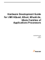
Hardware Development Guide
for i.MX 6Quad, 6Dual, 6DualLite,
6Solo Families of
Applications Processors
IMX6DQ6SDLHDG
Rev 1
06/2013
How to Reach Us:
Information in this document is provided solely to enable system and software
Home Page:
freescale.com
implementers to use Freescale products. There are no express or implied copyright
Web Support:
freescale.com/support
information in this document.
licenses granted hereunder to design or fabricate any integrated circuits based on the
Freescale reserves the right to make changes without further notice to any products
herein. Freescale makes no warranty, representation, or guarantee regarding the
suitability of its products for any particular purpose, nor does Freescale assume any
liability arising out of the application or use of any product or circuit, and specifically
disclaims any and all liability, including without limitation consequential or incidental
damages. “Typical” parameters that may be provided in Freescale data sheets and/or
specifications can and do vary in different applications, and actual performance may
vary over time. All operating parameters, including “typicals,” must be validated for each
customer application by customer’s technical experts. Freescale does not convey any
license under its patent rights nor the rights of others. Freescale sells products pursuant
to standard terms and conditions of sale, which can be found at the following address:
http://www.reg.net/v2/webservices/Freescale/Docs/TermsandConditions.htm.
Freescale and the Freescale logo are trademarks of Freescale Semiconductor, Inc.,
Reg. U.S. Pat. & Tm. Off. All other product or service names are the property of their
respective owners. ARM and Cortex are registered trademarks of ARM Limited.
© 2013 Freescale Semiconductor, Inc.
Document Number: IMX6DQ6SDLHDG
Rev 1, 06/2013
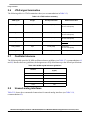
Contents
Paragraph
Number
Title
Page
Number
Chapter 1
About This Book
1.1
1.2
1.3
1.4
1.4.1
1.5
1.6
1.7
1.8
Overview.......................................................................................................................... 1-1
Devices supported............................................................................................................ 1-1
Essential reference ........................................................................................................... 1-1
Suggested reading ............................................................................................................ 1-1
General Information..................................................................................................... 1-1
Related documentation .................................................................................................... 1-2
Conventions ..................................................................................................................... 1-2
Signal conventions ........................................................................................................... 1-3
Acronyms and abbreviations ........................................................................................... 1-3
Chapter 2
Design Checklist
2.1
2.2
2.3
2.4
2.5
2.5.1
2.6
2.7
2.8
Design checklist overview ............................................................................................... 2-1
Design checklist tables..................................................................................................... 2-1
Bus isolation circuit ....................................................................................................... 2-11
DDR reference circuit .................................................................................................... 2-11
I2C address..................................................................................................................... 2-12
I2C clock speed and division factors (IFDR)............................................................. 2-13
JTAG signal termination ................................................................................................ 2-16
Oscillator tolerance ........................................................................................................ 2-16
Unused analog interfaces ............................................................................................... 2-16
Chapter 3
i.MX 6 Series Layout Recommendations
3.1
3.1.1
3.1.2
3.2
3.3
3.4
3.5
Basic design recommendations........................................................................................ 3-1
Fanout illustrations ...................................................................................................... 3-3
Placing decoupling capacitors ..................................................................................... 3-4
Stackup recommendations ............................................................................................... 3-4
DDR connection information........................................................................................... 3-6
DDR routing rules............................................................................................................ 3-8
Routing considerations .................................................................................................... 3-9
Hardware Development Guide for i.MX 6Dual/6Quad and i.MX 6Solo/6DualLite Applications Processors, Rev. 1
Freescale Semiconductor
iii
Contents
Paragraph
Number
3.5.1
3.5.2
3.5.3
3.5.4
3.5.5
3.5.6
3.5.7
3.5.8
3.5.9
3.6
3.7
3.7.1
3.7.2
3.7.3
3.8
3.9
3.10
3.11
3.12
3.13
3.14
3.15
3.16
3.17
Title
Page
Number
Swapping data lines ................................................................................................... 3-10
DDR3 (64 bits) T topology considerations................................................................ 3-10
DDR3 (64 bits) Fly-by topology considerations........................................................ 3-10
2-Gigabyte recommendations .................................................................................... 3-10
4-Gigabyte recommendations .................................................................................... 3-11
Four chips T topology routing examples ................................................................... 3-13
Eight chips fly-by topology routing examples........................................................... 3-17
High speed signal routing recommendations............................................................. 3-25
Ground plane recommendations ............................................................................... 3-25
DDR power recommendations....................................................................................... 3-28
PCI Express interface recommendations ...................................................................... 3-29
PCI Express general routing guidelines..................................................................... 3-29
PCI Express coupling lane......................................................................................... 3-30
Additional resources for PCI Express signal routing recommendations ................... 3-30
HDMI recommendations ............................................................................................... 3-30
SATA recommendations ................................................................................................ 3-30
LVDS recommendations ................................................................................................ 3-30
USB recommendations .................................................................................................. 3-31
Impedance signal recommendations .............................................................................. 3-31
Reference resistors ......................................................................................................... 3-32
ESD and radiated emissions recommendations ............................................................. 3-33
Component placement recommendations ...................................................................... 3-33
Reducing skew and phase problems in deferential pairs traces..................................... 3-33
Guideline for power net electrical performance ............................................................ 3-35
Chapter 4
Requirements for Power Management
4.1
4.1.1
4.1.2
4.2
4.3
4.4
4.5
Power management requirements overview .................................................................... 4-1
Voltage domains overview........................................................................................... 4-1
PF0100 overview ......................................................................................................... 4-1
Requirements for a generic interface between chip and PF0100..................................... 4-1
i.MX6 internal regulators................................................................................................. 4-4
Connection diagrams ....................................................................................................... 4-6
Video power recommendations........................................................................................ 4-8
Chapter 5
Using the Clock Connectivity Table
5.1
5.2
Root clocks ...................................................................................................................... 5-1
Waking the core up from stop mode ................................................................................ 5-2
Hardware Development Guide for i.MX 6Dual/6Quad and i.MX 6Solo/6DualLite Applications Processors, Rev. 1
iv
Freescale Semiconductor
Contents
Paragraph
Number
Title
Page
Number
Chapter 6
Using the IOMUX Design Aid
6.1
6.2
6.3
6.4
6.5
Compatibility across the i.MX 6 series families of processors........................................ 6-2
Application requirements................................................................................................. 6-2
IOMUX tool version ........................................................................................................ 6-2
IOMUX tool location....................................................................................................... 6-2
Learning to use the IOMUX tool ..................................................................................... 6-2
Chapter 7
Configuring JTAG Tools
7.1
7.2
7.3
7.4
7.5
7.6
JTAG tool requirements ................................................................................................... 7-1
Extra JTAG functionality ................................................................................................. 7-1
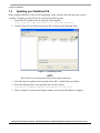
Updating your RealView ICE .......................................................................................... 7-2
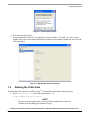
Defining the JTAG chain ................................................................................................. 7-3
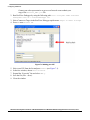
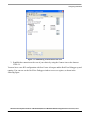
Reading a register with RealView Debugger v4.1........................................................... 7-6
CoreSight Base address references .................................................................................. 7-8
Chapter 8
Avoiding Board Bring-up Problems
8.1
8.2
8.3
8.4
8.5
Using a current monitor to avoid power pitfalls .............................................................. 8-1
Using a voltage report to avoid power pitfalls................................................................. 8-1
Checking for clock pitfalls............................................................................................... 8-2
Avoiding reset pitfalls ...................................................................................................... 8-3
Sample board bring-up checklist ..................................................................................... 8-4
Chapter 9
Understanding the IBIS Model
9.1
9.2
9.3
9.4
9.4.1
9.4.2
9.4.3
9.5
9.5.1
9.5.1.1
IBIS structure and content ............................................................................................... 9-1
Header Information.......................................................................................................... 9-2
Component and pin information ...................................................................................... 9-2
Model information ........................................................................................................... 9-4
IV information ............................................................................................................ 9-5
VT information ............................................................................................................ 9-5
Golden Model VT information .................................................................................... 9-7
Freescale naming conventions for model names and usage in i.MX6 IBIS file.............. 9-8
[Model Selector] ddr.................................................................................................... 9-8
DDR [Model Selector]............................................................................................. 9-8
Hardware Development Guide for i.MX 6Dual/6Quad and i.MX 6Solo/6DualLite Applications Processors, Rev. 1
Freescale Semiconductor
v
Contents
Paragraph
Number
9.5.1.2
9.5.2
9.5.3
9.5.4
9.5.5
9.5.6
9.6
9.7
9.8
Title
Page
Number
RGMII...................................................................................................................... 9-9
[Model Selector] gpio ................................................................................................ 9-10
[Model Selector] lvds................................................................................................. 9-11
[Model Selector] mlb ................................................................................................. 9-11
[Model Selector] USB ............................................................................................... 9-11
List of pins not modeled in the i.MX6 IBIS file........................................................ 9-12
Quality assurance for the IBIS models .......................................................................... 9-12
IBIS usage...................................................................................................................... 9-13
References...................................................................................................................... 9-13
Chapter 10
Using the Manufacturing Tool
10.1
10.2
10.3
Overview........................................................................................................................ 10-1
Feature summary............................................................................................................ 10-1
Other references ............................................................................................................. 10-2
Chapter 11
Using BSDL for Board-level Testing
11.1
11.2
11.3
11.4
11.5
11.6
BSDL overview ............................................................................................................. 11-1
How BSDL functions..................................................................................................... 11-1
Downloading the BSDL file .......................................................................................... 11-1
Pin coverage of BSDL ................................................................................................... 11-1
Boundary scan operation ............................................................................................... 11-2
I/O pin power considerations ......................................................................................... 11-2
Chapter 12
Using the RMII Interface
12.1
12.2
12.3
12.4
12.4.1
12.4.2
12.5
Overview........................................................................................................................ 12-1
Configuring the RMII signal connections ..................................................................... 12-2
Generating the reference clock ...................................................................................... 12-4
Generating the reference clock on chip ......................................................................... 12-4
Using the GPIO_16 pin to generate the reference clock ........................................... 12-5
Using RGMII_TX_CTL to generate the reference clock .......................................... 12-6
Using an external clock.................................................................................................. 12-7
Appendix A
Development Platforms
Hardware Development Guide for i.MX 6Dual/6Quad and i.MX 6Solo/6DualLite Applications Processors, Rev. 1
vi
Freescale Semiconductor
Contents
Paragraph
Number
Title
Page
Number
Appendix B
Revision History
Hardware Development Guide for i.MX 6Dual/6Quad and i.MX 6Solo/6DualLite Applications Processors, Rev. 1
Freescale Semiconductor
vii
Contents
Paragraph
Number
Title
Page
Number
Hardware Development Guide for i.MX 6Dual/6Quad and i.MX 6Solo/6DualLite Applications Processors, Rev. 1
viii
Freescale Semiconductor
Chapter 1
About This Book
1.1
Overview
This document’s purpose is to help hardware engineers design and test their i.MX 6 series processor based
designs. It provides information on board layout recommendations, design checklists to ensure first-pass
success and ways to avoid board bring-up problems. It also provides information on board-level testing
and simulation such as properly configuring JTAG tools, using BSDL for board-level testing, using the
IBIS model for electrical integrity simulation and more.
Engineers are expected to have a working understanding of board layouts and terminology, IBIS modeling,
BSDL testing and common board hardware terminology.
This guide is released along with relevant device-specific hardware documentation such as datasheets,
reference manuals and application notes available on www.freescale.com.
1.2
Devices supported
This Hardware Developer’s Guide currently supports the i.MX 6Quad, 6Dual, 6DualLite and 6Solo
families of application processors.
1.3
Essential reference
This guide is intended as a companion to the i.MX 6 series chip reference manuals and data sheets. For
reflow profile and thermal limits during soldering, see application note AN3298. These documents are
available on www.freescale.com.
1.4
Suggested reading
This section lists additional reading that provides background for the information in this manual as well as
general information about the architecture.
1.4.1
General Information
The following documentation provides useful information about the ARM processor architecture and
computer architecture in general:
For information about the ARM Cortex-A9 processor see:
http://www.arm.com/products/processors/cortex-a/cortex-a9.php
• Computer Architecture: A Quantitative Approach (Fourth Edition) - by John L. Hennessy and
David A. Patterson
Hardware Development Guide for i.MX 6Dual/6Quad and i.MX 6Solo/6DualLite Applications Processors, Rev. 1
Freescale Semiconductor
1-1
About This Book
•
Computer Organization and Design: The Hardware/Software Interface (Second Edition), by
David A. Patterson and John L. Hennessy
The following documentation provides useful information about high-speed board design:
• Right the First Time- A Practical Handbook on High Speed PCB and System Design Volumes I & II - Lee W. Ritchey (Speeding Edge) - ISBN 0-9741936- 0-72
• Signal and Power Integrity Simplified (2nd Edition) - Eric Bogatin (Prentice Hall)- ISBN
0-13-703502-0
• High Speed Digital Design- A Handbook of Black Magic - Howard W. Johnson & Martin
Graham (Prentice Hall) - ISBN 0-13-395724-1
• High Speed Signal Propagation- Advanced Black Magic - Howard W. Johnson & Martin
Graham - (Prentice Hall) - ISBN 0-13-084408-X
• High Speed Digital System Design- A handbook of Interconnect Theory and Practice - Hall,
Hall and McCall (Wiley Interscience 2000) - ISBN 0-36090-2
• Signal Integrity Issues and Printed Circuit Design - Doug Brooks (Prentice Hall) ISBN
0-13-141884-X
• PCB Design for Real-World EMI Control - Bruce R. Archambeault (Kluwer Academic
Publishers Group) - ISBN 1-4020-7130-2
• Digital Design for Interference Specifications- A Practical Handbook for EMI Suppression David L. Terrell & R. Kenneth Keenan (Newnes Publishing) - ISBN 0-7506-7282-X
• Electromagnetic Compatibility Engineering- Henry Ott (1st Edition - John Wiley and Sons) ISBN 0-471-85068-3
• Introduction to Electromagnetic Compatibility - Clayton R. Paul (John Wiley and Sons) - ISBN
978-0-470-18930-6
• Grounding & Shielding Techniques - Ralph Morrison (5th Edition - John Wiley & Sons) - ISBN
0-471-24518-6
• EMC for Product Engineers - Tim Williams (Newnes Publishing) - ISBN 0-7506- 2466-3
1.5
Related documentation
Freescale documentation is available from the sources listed on the back page of this guide.
Additional literature is published as new Freescale products become available. For a current list of
documentation, see www.freescale.com.
1.6
Conventions
This document uses the following notational conventions:
Courier
Used to indicate commands, command parameters, code examples, and file and
directory names.
Italics
Italics indicates command or function parameters
Bold
Function names are written in bold.
Hardware Development Guide for i.MX 6Dual/6Quad and i.MX 6Solo/6DualLite Applications Processors, Rev. 1
1-2
Freescale Semiconductor
About This Book
cleared/set
When a bit takes the value zero, it is said to be cleared; when it takes a value of
one, it is said to be set.
Instruction mnemonics are shown in lowercase bold
Book titles in text are set in italics
Internal signals are written in all lowercase
mnemonics
sig_name
nnnn nnnnh
0b
rA, rB
rD
REG[FIELD]
Denotes hexadecimal number
Denotes binary number
Instruction syntax used to identify a source GPR
Instruction syntax used to identify a destination GPR
Abbreviations for registers are shown in uppercase text. Specific bits, fields, or
ranges appear in brackets. For example, MSR[LE] refers to the little-endian mode
enable bit in the machine state register.
In some contexts, such as signal encodings, an unitalicized x indicates a don’t
care.
An italicized x indicates an alphanumeric variable
An italicized n indicates a numeric variable
x
x
n, m
NOTE
In this guide, notation for all logical, bit-wise, arithmetic, comparison, and
assignment operations follow C Language conventions.
1.7
Signal conventions
PWR_ON_RESET
_b, _B
signal_name
1.8
An overbar indicates that a signal is active when low
Alternate notation indicating an active-low signal
Lowercase italics is used to indicate internal signals
Acronyms and abbreviations
The following table defines the acronyms and abbreviations used in this document.
Table 1: Definitions and acronyms
Term
Definition
ARM®
Advanced RISC machines processor architecture
BGA
Ball grid array package
BOM
Bill of materials
BSDL
Boundary scan description language
CAN
Flexible Controller Area Network peripheral
CCM
Clock Controller Module
Hardware Development Guide for i.MX 6Dual/6Quad and i.MX 6Solo/6DualLite Applications Processors, Rev. 1
Freescale Semiconductor
1-3
About This Book
Table 1: Definitions and acronyms (continued)
CSI
MIPI camera serial interface
DDC
VESA Data Display Channel
DDR
Dual data rate DRAM
DDR3
DDR3 DRAM
DDR3L
Low voltage DDR3 DRAM
DDR3U
Ultra low voltage DDR3 DRAM
DRAM
Dynamic random access memory
DSI
MIPI display serial interface
ECSPI
Enhanced Configurable SPI peripheral
EDID
Extended Display Identification Data
EIM
External Interface Module
ENET
10/100/1000-Mbps Ethernet MAC peripheral
EPIT
Enhanced Periodic Interrupt Timer peripheral
ESR
Equivalent series resistance (of a crystal)
FSL
Freescale Semiconductor
GND
Ground
GPC
General Power Controller
GPIO
General-purpose input/output
HDCP
High-bandwidth Digital Content Protection
HDMI
High-definition multimedia interface
I2C
Inter-integrated circuit interface
IBIS
Input output buffer information specification
IOMUX
i.MX6 chip-level I/O multiplexing
JTAG
Joint Test Action Group
KPP
Keypad Port peripheral
LDB
LVDS Display bridge
LDO
Low drop-out regulator
LPCG
Low power clock gating
LPDDR2
Low-power DDR2 DRAM
LVDS
Low-voltage differential signaling
MLB
MediaLB 150 peripheral
MMDC
Multi Mode DDR Controller
ODT
On-die termination
OTP
One-time programmable
Hardware Development Guide for i.MX 6Dual/6Quad and i.MX 6Solo/6DualLite Applications Processors, Rev. 1
1-4
Freescale Semiconductor
About This Book
Table 1: Definitions and acronyms (continued)
PCB
Printed circuit board
PCIe
PCI Express
PCISig
Peripheral Component Interconnect Special Interest Group
PMIC
Power management integrated circuit
PoP
Package-on-package
POR
Power-on reset
RAM
Random access memory
RGMII
Reduced Gigabit Media Independent Interface (Ethernet)
RMII
Reduced Media Independent Interface (Ethernet)
ROM
Read-only memory
SATA
Serial ATA
SDMA
Smart Direct Memory Access Controller
UART
Universal asynchronous receiver/transmitter
USB
Universal Serial Bus
USB OTG
USB On-the-go
USB2.0
USB version 2.0 peripheral
VPU
Video processing units
Hardware Development Guide for i.MX 6Dual/6Quad and i.MX 6Solo/6DualLite Applications Processors, Rev. 1
Freescale Semiconductor
1-5
About This Book
Hardware Development Guide for i.MX 6Dual/6Quad and i.MX 6Solo/6DualLite Applications Processors, Rev. 1
1-6
Freescale Semiconductor
Chapter 2
Design Checklist
2.1
Design checklist overview
This chapter provides a design checklist for the following i.MX 6 series families of processors:
• i.MX 6Quad
• i.MX 6Dual
• i.MX 6DualLite
• i.MX 6Solo
The design checklist tables (Table 2-1–Table 2-14) contain recommendations for optimal design. Where
appropriate, the checklist tables also provide an explanation of the recommendation so that users have a
greater understanding of why certain techniques are recommended. All supplemental tables referenced by
the checklist appear in sections following the design checklist tables.
See also the application note Common Hardware Design for i.MX 6Dual/6Quad and i.MX
6Solo/6DualLite (AN4397).
2.2
Design checklist tables
Table 2-1. DDR recommendations
Checkbox
Recommendation
Explanation/supplemental recommendation
1. Connect ZQPAD to an external 240 Ω 1% resistor This is a reference used during DRAM output buffer
to GND.
driver calibration.
2. Connect DRAM_VREF to a source that is 50% of
the voltage value of NVCC_DRAM.
• The user may tie DDR_VREF to a precision external
resistor divider. Shunt each resistor with a
closely-mounted 0.1 μF capacitor. See Table 2-15 for
resistor values. Using resistors with recommended
tolerances ensures the ±2% DDR_VREF tolerance
per the DDR3 specification.
• The user can use a PMIC’s tracking regulator as
used on Freescale reference designs. A tracking
regulator is recommended as a reference for memory
configurations of more than four devices.
Hardware Development Guide for i.MX 6Dual/6Quad and i.MX 6Solo/6DualLite Applications Processors, Rev. 1
Freescale Semiconductor
2-1
Design Checklist
Table 2-1. DDR recommendations (continued)
Checkbox
Recommendation
Explanation/supplemental recommendation
3. Connect DRAM_RESET to a 10 kΩ 5% pulldown
resistor to GND.
• DDR3: DRAM_RESET should be pulled down to
meet the JEDEC sequence until the controller is
configured and starts driving. DRAM_RESET should
be kept high when DDR3 enters self-refresh mode.
• LPDDR2: DRAM_RESET should be left
unconnected.
Some Freescale reference designs use a 1% resistor
simply to consolidate the BOM.
DRAM_RESET is an active-low signal.
4. DRAM_SDCKE0 and DRAM_SDCKE1 no longer
require external 10 kΩ resistors to GND to minimize
current drain during deep sleep mode (DSM).
Both DRAM_SDCKE0 and DRAM_SDCKE1 have
on-chip pull-downs.
5. Make sure that the correct LPDDR2 function is
connected to the correct I/O. Note that this does not
necessarily correspond to the I/O name.
MMDC IO names are for the DDR3 default. When
LPDDR2 is selected, the I/O name (DDR3 MMDC PAD)
does not match with the LPDDR2 functionality. See the
“LPDDR2 and DDR3 pin mux mapping” table in the
“Multi Mode DDR Controller (MMDC)” chapter in your
chip reference manual.
Table 2-2. EIM recommendations for developer’s boot modes
Checkbox
Recommendation
1. When EIM boot signals are used as the system’s
EIM signals, other functions, or GPIO outputs after
boot, use a passive resistor network to select the
desired boot mode for development boards.
Explanation/supplemental recommendation
Because only resistors are used, EIM bus loads can
cause current drain, leading to higher (false) supply
current measurements. Each EIM boot signal should
connect to a series resistor to isolate the bus from the
resistors and/or switchers; see Figure 2-1. Each
configured EIM boot signal sees either a 14.7 kΩ
pulldown or a 4.7 kΩ pullup. For each switch-enabled
pulled-up signal, the supply is presented with a 10 kΩ
current load.
Hardware Development Guide for i.MX 6Dual/6Quad and i.MX 6Solo/6DualLite Applications Processors, Rev. 1
2-2
Freescale Semiconductor
Design Checklist
Table 2-2. EIM recommendations for developer’s boot modes (continued)
Checkbox
Recommendation
Explanation/supplemental recommendation
2. To reduce incorrect boot-up mode selections, do
one of the following:
• Use EIM boot interface lines only as processor
outputs. Ensure EIM boot interface lines are not
loaded down such that the level is interpreted as
low during power-up, when the intent is to be a
high level, or vice versa.
• If an EIM boot signal must be configured as an
input, isolate the EIM signal from the target driving
source with one analog switch and apply the logic
value with a second analog switch. Alternately,
peripheral devices with three-state outputs may be
used; ensure the output is high-impedance during
the boot up interval.
Using EIM boot interface lines as inputs may result in a
wrong boot up due to the source overcoming the pull
resistor value. A peripheral device may require the EIM
signal to have an external or on-chip resistor to minimize
signal floating.
If the usage of the EIM boot signal affects the peripheral
device, then an analog switch, open collector buffer, or
equivalent should isolate the path. A pullup or pulldown
resistor at the peripheral device may be required to
maintain the desired logic level. Review the switch or
device data sheet for operating specifications.
3. The BOOT_CFG signals are required for proper
functionality and operation and should not be left
floating.
See the “System Boot” chapter in your chip reference
manual for the correct boot configuration. Note that an
incorrect setting may result from an improper booting
sequence.
Table 2-3. Boot mode input recommendations
Checkbox
Recommendation
Explanation/supplemental recommendation
1. For BOOT_MODE1 and BOOT_MODE0, use one of
the following options to achieve logic 0:
• Tie to GND through any size external resistor
• Tie directly to GND
• Float
For logic 1, use one of the following:
• Tie directly to the VDD_SNVS_IN rail
• Tie to the VDD_SNVS_IN rail through an external
resistor 10 kΩ. A value of 4.7 kΩ is preferred in
high-noise environments.
If switch control is desired, no external pulldown
resistors are necessary. Simply connect SPST switches
directly to the VDD_SNVS_IN rail. If desired, a 4.7 kΩ
to 10 kΩ series resistor can be used when current drain
is critical.
Boot inputs BOOT_MODE1 and BOOT_MODE0 each
have on-chip pulldown devices with a nominal value of 100
kΩ, a projected minimum of 60 kΩ, and a projected
maximum of 140 kΩ.
Be aware that when these are logic high, current is drawn
from the VDD_SNVS supply.
In production, when on-chip fuses determine the boot
configuration, both boot mode inputs can be no connects.
Hardware Development Guide for i.MX 6Dual/6Quad and i.MX 6Solo/6DualLite Applications Processors, Rev. 1
Freescale Semiconductor
2-3
Design Checklist
Table 2-4. I2C recommendations
Checkbox
Recommendation
1. Verify the target I2C interface clock rates.
Explanation/supplemental recommendation
The bus can only operate as fast as the slowest peripheral
on the bus. If faster operation is required, move the slow
devices to another I2C port.
2. Verify that the target I2C address range is supported These chips support up to:
• Three I2C ports for the i.MX 6Quad and 6Dual families
and does no conflict with other peripherals. If there is
an unavoidable address conflict, move the offending
• Four I2C ports for the i.MX 6DualLite and 6Solo
2
device to another I C port. See Table 2-16.
families.
If it is undesirable to move a conflicting device to another
I2C port, review the peripheral operation to see if it
supports remapping the address.
3. Do not place more than one set of pullup resistors on This can result in excessive loading. Good design
practice is to place one pair of pullups only.
the I2C lines.
Table 2-5. JTAG recommendations
Checkbox
Recommendation
Explanation/supplemental recommendation
1. Do not use external pullup or pulldown resistors on
JTAG_TDO.
JTAG_TDO is configured with an on-chip keeper circuit
such that the floating condition is actively eliminated if an
external pull resistor is not present. An external pull
resistor on JTAG_TDO is detrimental. See Table 2-19 for
a summary of the JTAG interface.
2. Ensure that the on-chip pullup/pulldown
configuration is followed. If external resistors are used
with JTAG signals, with the exception of JTAG_TDO.
For example, do not use an external pulldown on an
input that has an on-chip pullup.
External resistors can be used with all JTAG signals
except JTAG_TDO, but they are not required. See
Table 2-19 for a summary of the JTAG interface.
3. JTAG_MOD may be referred to as SJC_MOD in
some documents. Both names refer to the same signal.
JTAG_MOD should be externally connected to GND for
normal operation in a system. Termination to GND
through an external pulldown resistor is allowed.
Use ≤ 4.7 kΩ.
When JTAG_MOD is low, the JTAG interface is configured
for common software debug, adding all the system taps to
the chain.
When JTAG_MOD is high, the JTAG interface is
configured to a mode compliant with the IEEE 1149.1
standard.
Hardware Development Guide for i.MX 6Dual/6Quad and i.MX 6Solo/6DualLite Applications Processors, Rev. 1
2-4
Freescale Semiconductor
Design Checklist
Table 2-6. Power and decouple recommendations
Checkbox
Recommendation
Explanation/supplemental recommendation
1. Comply with the power-up sequence guidelines as
described in the data sheet to guarantee reliable
operation of the device.
Any deviation from these sequences may result in the
following situations:
• Excessive current during power-up phase
• Prevention of the device from booting
• Irreversible damage to the processor (worst-case
scenario)
2. Do not overload coin cell backup power rail
VDD_SNVS_IN. Note that the following I/Os are
associated with VDD_SNVS_IN; most inputs have
on-chip pull resistors and do not require external
resistors:
• POR_B – on-chip pullup; see Table 2-8 #1
• ONOFF – on-chip pullup; see Table 2-8 #2
• BOOT_MODE0 – on-chip pulldown; see Table 2-3
#1
• BOOT_MODE1 – on-chip pulldown; see Table 2-3
#1
• TAMPER – on-chip pulldown
• PMIC_STBY_REQ – push-pull output
• PMIC_ON_REQ – push-pull output
• TEST_MODE – on-chip pulldown; see Table 2-14 #1
Freescale PMIC PMPF0100 VSNVS regulator is rated to
supply 400 μA output current under worst-case operating
conditions. The VDD_SNVS_IN regulator can supply
larger current in transient situations without damaging the
regulator.
Concerning i.MX6:
• When VDD_SNVS_IN = VDD_HIGH_IN, SNVS
domain current is drawn from both equally.
• When VDD_HIGH_IN > VDD_SNVS_IN,
VDD_HIGH_IN supplies all SNVS domain current and
current flows into VDD_SNVS_IN to charge a coin cell
battery.
• When VDD_SNVS_IN > VDD_HIGH_IN,
VDD_SNVS_IN supplies current to SNVS, and some
current flows into VDD_HIGH_IN.
Note:VDD_HIGH_IN must be valid (above the internal
detector threshold, 2.4 V typ) for the current flow to
occur. Thus, current flow only happens when
VDD_HIGH_IN is powered to a level below
VDD_SNVS_IN. If VDD_HIGH_IN is off or low, no extra
current is drawn from VDD_SNVS_IN. The whole
circuit assumes it is charging a coin cell and starts
charging when VDD_HIGH_IN is valid. If you are
driving VDD_SNVS_IN with a non-battery power
source, it must be at the same level as VDD_HIGH_IN
or current will flow between them.
• When VDD_SNVS_IN is not powered by a battery, it is
recommended that VDD_SNVS_IN = VDD_HIGH_IN.
If VDD_SNVS_IN is tied to a battery, the battery eventually
discharges to a value equal to that of VDD_HIGH_IN and
never subsequently charges above VDD_HIGH_IN.
The battery chemistry may add restrictions to
VDD_HIGH_IN’s voltage range. External charging
components should be based on the battery
manufacturer's specifications.
Hardware Development Guide for i.MX 6Dual/6Quad and i.MX 6Solo/6DualLite Applications Processors, Rev. 1
Freescale Semiconductor
2-5
Design Checklist
Table 2-6. Power and decouple recommendations (continued)
Checkbox
Recommendation
Explanation/supplemental recommendation
3. Only one 22 μF bulk capacitor should be connected
to each of these on-chip LDO regulator outputs:
• VDD_ARM_CAP
• VDDARM23_CAP
• VDD_SOC_CAP
• VDD_PU_CAP
A 22 μF bulk capacitor must be placed as near as
possible with pins/vias. The distance should be less
than 50mil between bulk cap and VDD_xx_CAP pins.
Decoupling capacitors such as 0.1 μF or 0.22 μF should
also be used.
If the nominal capacitance value is larger than
recommended, power-up ramp time is excessive and
operation cannot be guaranteed. Note that the ramp up
time is constant. Larger capacitors mean more inrush
current. Select small capacitors with low ESR (equivalent
series resistance).
The 22 μF bulk capacitors should be placed as close as
possible to the associated VDD_xx_CAP ball, with trace
widths and via sizes appropriate to the expected current
draw. A trace length of less than 50 mil is recommended.
Do not connect any loads to these LDO outputs:
VDDARM_CAP, VDDARM23_CAP, or VDDPU_CAP.
VDDSOC_CAP is restricted to MX6 loads.
4. Only one 10 μF bulk capacitor should be connected
to each of these on-chip LDO regulator outputs:
• VDD_HIGH_CAP
• NVCC_PLL_OUT
• VDD_USB_CAP
Decoupling capacitors such as 0.1 μF or 0.22 μF should
also be used.
If the nominal capacitance value is larger than
recommended, power-up ramp time is excessive and
operation cannot be guaranteed. Select small capacitors
with low ESR.
These LDOs should only be used to power the loads as
described in the reference manual or data sheet. Do not
connect any loads to these LDO outputs:
NVCC_PLL_OUT or VDDUSB_CAP. VDDHIGH_CAP is
restricted to MX6 loads.
5. One 0.22 μF decoupling capacitor should be
connected to VDD_SNVS_CAP, an on-chip LDO
regulator output. A bulk capacitor is not necessary.
If the nominal value is larger than recommended,
power-up/down ramp time is excessive and
suspend/resume operation cannot be guaranteed. Select
a small capacitor with low ESR.
Note: Do not connect any loads to VDD_SNVS_CAP.
6. Maximum ripple voltage requirements.
Common requirement for ripple noise should be less than
5% Vp-p of supply voltage average value.
Related power rails affected: all VDD_xxx_IN and
VDD_xxx_CAP.
7. NVCC_LVDS2P5 must be powered-on even when
not using the LVDS interface.
The DDR pre-drivers share the NVCC_LVDS2P5 power
rail with the LVDS interface. VDDHIGH_CAP can be
utilized as the power source; tie NVCC_LVDS2P5 to
VDDHIGH_CAP.
8. Account for the different power design on
NVCC_EIM between i.MX 6Quad and 6Dual chips and
i.MX 6DualLite and 6Solo chips.
• i.MX 6Quad and 6Dual chips can support three different
EIM power rail voltage levels: NVCC_EIM0(K19),
NVCC_EIM1(L19), and NVCC_EIM2(M19).
• i.MX 6DualLite and 6Solo chips support one EIM power
rail: NVCC_EIM (K19, L19, M19). The three power
contacts must be connected to same power supply.
9. If VDD_SNVS_IN is directly supplied by a coin cell, a
schottky diode is required between VDD_HIGH_IN and
VDD_SNVS_IN. The cathode is connected to
VDD_SNVS_IN.
Alternately, VDD_HIGH_IN and VDD_SNVS_IN can be
tied together if the real-time clock function is not
needed during system power-down.
When no power is supplied to VDD_VSNVS_IN, the diode
limits the voltage difference between the two on-chip
SNVS power domains to approximately 0.3 V. The
processor is designed to allow current flow between the
two SNVS power domains proportional to the voltage
difference.
Hardware Development Guide for i.MX 6Dual/6Quad and i.MX 6Solo/6DualLite Applications Processors, Rev. 1
2-6
Freescale Semiconductor
Design Checklist
Table 2-7. Oscillator and clock recommendations
Checkbox
Recommendation
Explanation/supplemental recommendation
1. Precision 32.768 kHz oscillator
Connect a crystal between RTC_XTALI and
RTC_XTALO. Choose a crystal with a maximum of
100 kΩ ESR (equivalent series resistance) and follow
the manufacturer’s recommendation for loading
capacitance.
Do not use an external biasing resistor because the
bias circuit is on-chip.
The capacitors implemented on either side of the crystal
are about twice the crystal load capacitance. To hit the
target oscillation frequency, board capacitors need to be
reduced to compensate for board and chip parasitic
capacitance; typically 15–16 pF is employed.
The integrated oscillation amplifier has an on-chip
self-biasing scheme, but is high-impedance (relatively
weak) to minimize power consumption. Care must be
taken to limit parasitic leakage from RTC_XTALI and
RTC_XTALO to either power or ground (> 100 MΩ) as
this negatively affects the amplifier bias and causes a
reduction of startup margin.
Use short traces between the crystal and the processor,
with a ground plane under the crystal, load capacitors,
and associated traces.
2. External kilohertz source
If feeding an external clock into the device,
RTC_XTALI can be driven DC-coupled with
RTC_XTALO floated or driven with a complimentary
signal.
The voltage level of this driving clock should not exceed
the voltage of VDD_SNVS_CAP and the frequency
should be <100 kHz under typical conditions. Do not
exceed VDD_SNVS_CAP or damage/malfunction may
occur. The RTC_XTALI signal should not be driven if the
VDD_SNVS_CAP supply is off. This can lead to damage
or malfunction.
For RTC_XTALI VIL and VIH voltage levels, see the latest
i.MX 6 series datasheet available at www.freescale.com.
Note that if this external clock is stopped, the internal ring
oscillator starts automatically.
3. Loose-tolerance 40 kHz oscillator
An on-chip loose-tolerance ring oscillator is available
of approximately 40 kHz. If RTC_XTALI is tied to GND
and RTC_XTALO is floating, the on-chip oscillator is
automatically engaged.
When a high-accuracy real-time clock is not required, the
system may use the on-chip 40 kHz oscillator. The
tolerance is ± 50%.
The ring oscillator starts faster than an external crystal
and is used until the external crystal reaches stable
oscillation. The ring oscillator also starts automatically if
no clock is detected at RTC_XTALI at any time.
4. Precision 24 MHz oscillator
Connect a fundamental-mode crystal between XTALI
and XTALO. An 80 Ω typical ESR crystal rated for a
maximum drive level of 250 μW is acceptable.
Alternately, a 50 Ω typical ESR crystal rated for a
maximum drive level of 200 μW may be used. See the
engineering bulletin EB830 on www.freescale.com for
additional options.
Freescale BSP software requires 24 MHz on this clock.
This clock is used as a reference for USB, PCIe, and
SATA, so there are strict frequency tolerance and jitter
requirements. See Table 2-20 for guidelines. See the
crystal oscillator (XTALOSC) reference manual chapter
and relevant interface specification chapters for details.
To access a calculator for the 24 MHz crystal drive level,
see EB830 on the i.MX Community.
5. External megahertz source
For XTALI VIL and VIH voltage levels, see the latest i.MX
If feeding an external clock into the device, XTALI can 6 series datasheet. This clock is used as a reference for
be driven DC-coupled with XTALO floated.
USB, PCIe, and SATA, so there are strict frequency
tolerance and jitter requirements. See Table 2-20 for
guidelines. See the crystal oscillator (XTALOSC)
reference manual chapter and relevant interface
specification chapters for details.
Hardware Development Guide for i.MX 6Dual/6Quad and i.MX 6Solo/6DualLite Applications Processors, Rev. 1
Freescale Semiconductor
2-7
Design Checklist
Table 2-7. Oscillator and clock recommendations (continued)
Checkbox
Recommendation
Explanation/supplemental recommendation
6. CLK1_P/CLK1_N and CLK2_P/CLK2_N are LVDS
input/output differential pairs compatible with
TIA/EIA-644 standard. The frequency range is 0 to
600 MHz.
Alternatively, a single-ended signal can be used to
drive a CLKx_P input. In this case, the corresponding
CLKx_N input should be tied to a constant voltage
level equal to 50% of VDD_HIGH_CAP. Termination
should be provided with high-frequency signals.
See the LVDS pad electrical specification in the data
sheet for further details.
After initialization, the CLKx inputs/outputs can be
disabled (if not used) by the PMU_MISC1 register. If
unused, any or both of the CLKx_N/P pairs may be left
floating.
The clock inputs/outputs are general-purpose differential
high-speed clock Input/outputs.
Any or both of them can be configured:
• As inputs to feed external reference clocks to the
on-chip PLLs and/or modules, for example as
alternate reference clock for PCIe or/and SATA or
video/audio interfaces.
• As outputs to be used as either a reference clock or as
a functional clock for peripherals, for example an
output of the PCIe master clock (root complex use).
See the chip reference manual for details on the
respective clock trees.
7. Bias XTALI with a 2.2 MΩ resistor to GND. Mount
the resistor close to the XTALI ball.
The XTALI bias must be adjusted externally to ensure
reasonable start-up time. Without the resistor, start-up
time may be 200 ms or more.
Table 2-8. Reset and ONOFF recommendations
Checkbox
Recommendation
Explanation/supplemental recommendation
1. The POR_B input must be asserted low at power-up
and remain asserted until after the last power rail for
devices required for system boot are at their working
voltage.
A reset switch may be wired to the chip’s POR_B, which
is a cold-reset negative-logic input that resets all modules
and logic in the IC. POR_B may be used in addition to
internally generated power-on reset signal (logical AND,
both internal and external signals are considered active
low).
2. For portable applications, the ONOFF input may be
connected to an ON/OFF SPST push-button switch.
On-chip debouncing is provided, and this input has an
on-chip pullup.
If not used, ONOFF should be a no connect.
A brief connection to GND in OFF mode causes the
internal power management state machine to change
state to ON.
In ON mode, a brief connection to GND generates an
interrupt (intended to be a software-controllable
power-down).
An approximate 5 second or more connection to GND
causes a forced OFF.
Hardware Development Guide for i.MX 6Dual/6Quad and i.MX 6Solo/6DualLite Applications Processors, Rev. 1
2-8
Freescale Semiconductor
Design Checklist
Table 2-9. Gigabit Ethernet Recommendations
Checkbox
Recommendation
Explanation/supplemental recommendation
1. This chip requires a 125 MHz reference clock
feeding the ENET_REF_CLK input. This reference
clock should be sourced from an external 125 MHz
oscillator or an external PHY.
Designers should be aware of the 125 MHz reference
output level of the PHY because ENET_REF_CLK is
on the NVCC_ENET supply rail, not the NVCC_RGMII
rail.
If NVCC_ENET is powered at 3.3 V, the minimum VIH
level is 70% of 3.3 V or 2.3 V. Designers should ensure
that there is margin to this minimum value. A starting value
could be 500 mV margin, resulting in a requirement of
2.8 V for the logic high. See the Freescale Smart Devices
development designs for a suitable low-cost level
translator.
2. For IEEE-1588 operation, the GPIO_16 ball must be This allows use of time stamping on the RGMII interface.
configured as either one of the following:
• A no connect to allow the internal time stamp clock
to route through its IOMUX cell to the RGMII
interface
• Driven by an external clock source for the time
stamp
Table 2-10. PCIe recommendations
Checkbox
Recommendation
Explanation/supplemental recommendation
1. Termination is required on the differential clock lines.
Connect two 49.9 Ω resistors, one between REFCLKand GND, the other between REFCLK+ and GND.
Alternately, Connect a 100 Ω resistor between
REFCLK- and REFCLK+.
These termination resistors should be placed as close as
possible to the receiver device inputs in case the chip
LVDS clock outputs are used as the REFCLK source for
the PCIe endpoint device.
2. The differential transmitter must be ac coupled. Use To ensure PCIe specification compliance, ac coupling is
a 0.1 uF-series capacitor on PCIE_TXP and a second required at each transmitter. The receiver must be dc
0.1 uF on PCIE_TXM.
coupled.
Table 2-11. HDMI recommendations
Checkbox
Recommendation
1. The designer must ensure that a suitable level shifter
and driver be used to interface the chip’s I2C with the
HDMI monitor.
In addition, ESD (electrostatic discharge) protection
must be used on all HDMI single-ended and differential
signals mounted near the board’s HDMI connector.
Explanation/supplemental recommendation
The i.MX 6 processors’ I2C cannot operate at the 5 V
required by HMDI EDID. The i.MX 6 processors’ supply
limit is 3.6 V maximum.
The designer could consider the ON Semiconductor
CM2020 for ESD protection and I2C level conversion.
Note: Freescale cannot recommend one supplier over
another and does not suggest that this is the only
HDMI interface chip supplier.
When HDCP is enabled, a dedicated I2C is controlled by
2. DDC (EDID) must be on a dedicated I2C
(DDC_SCL/DDC_SDA) port when HDCP
the HDMI PHY to exchange the HDCP encryption key and
(High-Bandwidth Digital Content Protection) is enabled. must sync several times per second. DDC does not
behave like a common I2C and cannot be controlled by the
ARM® CPU with HDCP enabled.
Hardware Development Guide for i.MX 6Dual/6Quad and i.MX 6Solo/6DualLite Applications Processors, Rev. 1
Freescale Semiconductor
2-9
Design Checklist
Table 2-12. USB recommendations
Checkbox
Recommendation
Explanation/supplemental recommendation
1. USB OTG
The processor should turn VBUS on as required.
To comply with the USB OTG specification, the VBUS
supply on the OTG connector should default to off when
the boards power up.
2. USB Host
Tie USB_H1_VBUS to an unswitched 5 V supply for the
USB_H1_VBUS should be directly connected to a 5 V typical use case. However, if the your system is a USB
supply.
device, then USB_H1_VBUS may be a no connect.
Table 2-13. Reference resistor recommendations
Checkbox
Recommendation
Explanation/supplemental recommendation
1. HDMI_REF – Connect an external 1.6 kΩ 1%
resistor to GND.
If HDMI is unused, the reference resistor may be
populated if desired for manufacturability purposes, or left
no-connect for cost savings.
2. SATA_REXT – Connect an external 191 Ω 1%
resistor to GND.
The impedance calibration process requires connection of
this reference resistor.
If SATA is unused, the reference resistor may be
populated if desired for manufacturability purposes, or left
no-connect for cost savings.
3. PCIE_REXT – Connect an external 200 Ω 1%
resistor to GND.
The impedance calibration process requires connection of
this reference resistor.
If PCIe is unused, the reference resistor may be populated
if desired for manufacturability purposes, or left
no-connect for cost savings.
4. CSI_REXT – Connect an external 6.04 kΩ 1%
resistor to GND.
If CSI is unused, the reference resistor may be populated
if desired for manufacturability purposes, or left
no-connect for cost savings.
5. DSI_REXT – Connect an external 6.04 kΩ 1%
resistor to GND.
If DSI is unused, the reference resistor may be populated
if desired for manufacturability purposes, or left
no-connect for cost savings.
Table 2-14. Miscellaneous recommendations
Checkbox
Recommendation
Explanation/supplemental recommendation
1. The TEST_MODE input is internally connected to an This input is reserved for Freescale manufacturing use.
on-chip pulldown device. The user can either float this
signal or tie it to GND.
2. For termination of unused analog interfaces, see
Table 2-21.
—
3. VDD_FA and FA_ANA should be tied to GND.
These inputs are reserved for Freescale manufacturing
use. Best practice is to tie them to ground to avoid floating
inputs.
Hardware Development Guide for i.MX 6Dual/6Quad and i.MX 6Solo/6DualLite Applications Processors, Rev. 1
2-10
Freescale Semiconductor
Design Checklist
Table 2-14. Miscellaneous recommendations (continued)
Checkbox
2.3
Recommendation
Explanation/supplemental recommendation
4. GPANAIO must be a no connect.
This output is reserved for Freescale manufacturing use.
5. NC contacts are no connect and should be floated.
Depending on the feature set, some versions of the IC
may have NC contacts connected inside the BGA.
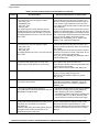
Bus isolation circuit
The following figure provides supporting information for Table 2-2, recommendation #1
Figure 2-1. Boot configuration for development mode
2.4
DDR reference circuit
The following table is a resistor chart (see Table 2-1 recommendation #2). The recommendations are
appropriate for designs with DDR memory chips with a maximum Vref input current of 2µA each.
Hardware Development Guide for i.MX 6Dual/6Quad and i.MX 6Solo/6DualLite Applications Processors, Rev. 1
Freescale Semiconductor
2-11
Design Checklist
Ä
Table 2-15. DDR Vref resistor sizing guideline
2.5
Number of DRAM with 2 μA Vref
input current
Resistor divider value
(2 resistors)
2
≤1.21 kΩ 1%
2
≤1.54 kΩ 0.5%
2
≤2.32 kΩ 0.1%
4
≤768 Ω 1%
4
≤1 kΩ 0.5%
4
≤1.5 kΩ 0.1%
I2C address
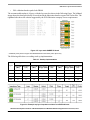
The following table shows a spreadsheet approach to avoid I2C conflicts as referenced in Table 2-4
recommendation #2.
NOTE
The example in this section only applies to the Freescale reference design
board.
Notice that although there are no slave address conflicts, the shaded cell in the table highlights a potential
bus speed issue as discussed in Table 2-4. The AM-FM tuner limits the maximum bus rate to 250 kbps,
but the bus data rate cannot exceed the slowest peripheral on the bus.
If the system cannot tolerate the 250 kbps rate for proper operation, the AM-FM tuner must be moved to
another I2C port. If the I2C bus rate exceeded the AM-FM tuner module’s maximum bus rate, the I2C bus
operation might fail or become unpredictable. The slow peripheral may unpredictably take over the bus or
might malfunction in some other way.
Table 2-16. I2C bus example spreadsheet
Peripheral
Bus activity level
Speed (kbps)
Slave addresses supported on
the peripheral
(hex)
Selected system
address (hex)
PMIC
Low
400
68
68
Port Expander
Low
400
30, 32, 34
30
AM-FM Tuner
Med
250
C0, C2, C4, C6
C0
A/D Converter
Med
400
40, 42
40
Audio CODEC
Low
400
90, 92, 94, 96
90
Hardware Development Guide for i.MX 6Dual/6Quad and i.MX 6Solo/6DualLite Applications Processors, Rev. 1
2-12
Freescale Semiconductor
Design Checklist
Assuming the system can function properly with a reduced bus rate of 250 kbps, the following table
provides a possible I2C port usage table.
Table 2-17. I2C port usage scenario
i.MX6 I2C ports
Ball name
Function
Speed (kbps)
Port 2
KEY_ROW3
I2C2_SDA
250
Port 2
EIM_EB2
I2C2_SCL
250
Port 1
Port 1
Port 3
Port 3
2.5.1
I2C clock speed and division factors (IFDR)
The I2C clock is sourced from PERCLK_CLK_ROOT which is routed from IPG_CLK_ROOT. The I2C
clock frequency can be easily obtained using the following formula:
I2C clock Frequency = (PERCLK_ROOT frequency)/(division factor corresponding to IFDR)
By default, the IPG_CLK_ROOT and PERCLK_CLK_ROOT frequencies are set to 49.5MHz, where the
root clock is sourced from PLL2’s PFD2. Obtaining the frequencies can be accomplished using the
following:
PLL2 = 528MHz
PLL2_PFD2 = 528MHz * 18 / 24 = 396MHz
IPG_CLK_ROOT = (PLL2_PFD2 / ahb_podf )/ ipg_podf = (396MHz/4)/2 = 49.5MHz
PER_CLK_ROOT = IPG_CLK_ROOT/perclk_podf = 49.5MHz/1 = 49.5MHz
NOTE
The above calculation assumes that the default CCM register settings,
routing, and division factors are used. If different routing, PFD values,
and/or division factors are used, the user must adjust the parameters
accordingly to calculate the correct clock frequency.
IFDR, division factor and resulting I2C CLK frequencies are indicated in the table below. Resulting
frequencies will vary according to the PERCLK_CLK_ROOT frequencies selected.
Hardware Development Guide for i.MX 6Dual/6Quad and i.MX 6Solo/6DualLite Applications Processors, Rev. 1
Freescale Semiconductor
2-13
Design Checklist
Table 2-18 assumes PERCLK_CLK_ROOT = 49.5MHz.
Table 2-18. IFDR1
IFDR
Division factor
Frequency (kHz)
0
30
1650
1
32
1546.875
2
36
1375
3
42
1178.571
4
48
1031.25
5
52
951.9231
6
60
825
7
72
687.5
8
80
618.75
9
88
562.5
A
104
475.9615
B
128
386.7188
C
144
343.75
D
160
309.375
E
192
257.8125
F
240
206.25
10
288
171.875
11
320
154.6875
12
384
128.9063
13
480
103.125
14
576
85.9375
15
640
77.34375
16
768
64.45313
17
960
51.5625
18
1152
42.96875
19
1280
38.67188
1A
1536
32.22656
1B
1920
25.78125
1C
2304
21.48438
1D
2560
19.33594
1E
3072
16.11328
1F
3840
12.89063
Hardware Development Guide for i.MX 6Dual/6Quad and i.MX 6Solo/6DualLite Applications Processors, Rev. 1
2-14
Freescale Semiconductor
Design Checklist
Table 2-18. IFDR1 (continued)
1
20
22
2250
21
24
2062.5
22
26
1903.846
23
28
1767.857
24
32
1546.875
25
36
1375
26
40
1237.5
27
44
1125
28
48
1031.25
29
56
883.9286
2A
64
773.4375
2B
72
687.5
2C
80
618.75
2D
96
515.625
2E
112
441.9643
2F
128
386.7188
30
160
309.375
31
192
257.8125
32
224
220.9821
33
256
193.3594
34
320
154.6875
35
384
128.9063
36
448
110.4911
37
512
96.67969
38
640
77.34375
39
768
64.45313
3A
896
55.24554
3B
1024
48.33984
3C
1280
38.67188
3D
1536
32.22656
3E
1792
27.62277
3F
2048
24.16992
Shaded cells indicate frequency is outside of the range that guarantees operation.
Hardware Development Guide for i.MX 6Dual/6Quad and i.MX 6Solo/6DualLite Applications Processors, Rev. 1
Freescale Semiconductor
2-15
Design Checklist
2.6
JTAG signal termination
The following table is a JTAG termination chart (see recommendations in Table 2-5).
Table 2-19. JTAG interface summary
2.7
JTAG signal
I/O type
On-chip termination
External termination
JTAG_TCK
Input
47 kΩ pullup
Not required;
can use 10 kΩ pullup
JTAG_TMS
Input
47 kΩ pullup
Not required;
can use 10 kΩ pullup
JTAG_TDI
Input
47 kΩ pullup
Not required;
can use 10 kΩ pullup
JTAG_TDO
3-state output
Keeper
JTAG_TRSTB
Input
47 kΩ pullup
Not required;
can use 10 kΩ pullup
JTAG_MOD
Input
100 kΩ pullup
Use 1 kΩ pulldown or tie to GND
Do not use pullup or pulldown
Oscillator tolerance
The following table provides 24 MHz oscillator tolerance guidelines (see Table 2-7, recommendations #4
and #5). Because these are guidelines, the designer must verify all tolerances per the official specifications.
Table 2-20. 24 MHz crystal tolerance guidelines
2.8
Interface
Tolerance
(± ppm)
Ethernet
50
HDMI
100
SATA
350
USB2.0
500
PCIe
300
Unused analog interfaces
Table 2-21 shows the recommended connections for unused analog interfaces (see Table 2-14,
recommendation #2).
Hardware Development Guide for i.MX 6Dual/6Quad and i.MX 6Solo/6DualLite Applications Processors, Rev. 1
2-16
Freescale Semiconductor
Design Checklist
Table 2-21. Recommended connections for unused analog interfaces
Module
CCM
Contact name
Recommendations if unused
CLK1_N, CLK1_P, CLK2_N, CLK2_P
Float
CSI
CSI_CLK0M, CSI_CLK0P, CSI_D0M, CSI_D0P, CSI_D1M, CSI_D1P, CSI_D2M,
CSI_D2P, CSI_D3M, CSI_D3P, CSI_REXT
Float
DSI
DSI_CLK0M, DSI_CLK0P, DSI_D0M, DSI_D0P, DSI_D1M, DSI_D1P,
DSI_REXT
Float
HDMI_CLKM, HDMI_CLKP, HDMI_D0M, HDMI_D0P, HDMI_D1M, HDMI_D1P,
HDMI_D2M, HDMI_D2P, HDMI_DDCEC, HDMI_HPD, HDMI_REF
Float
HDMI
HDMI_VP, HDMI_VPH
Ground
LDB
LVDS0_CLK_N, LVDS0_CLK_P, LVDS0_TX0_N, LVDS0_TX0_P,
LVDS0_TX1_N, LVDS0_TX1_P, LVDS0_TX2_N, LVDS0_TX2_P,
LVDS0_TX3_N, LVDS0_TX3_P, LVDS1_CLK_N, LVDS1_CLK_P,
LVDS1_TX0_N, LVDS1_TX0_P, LVDS1_TX1_N, LVDS1_TX1_P,
LVDS1_TX2_N, LVDS1_TX2_P, LVDS1_TX3_N, LVDS1_TX3_P
Float
MLB
MLB_CN, MLB_CP, MLB_DN, MLB_DP, MLB_SN, MLB_SP
Float
PCIe
PCIE_REXT, PCIE_RXM, PCIE_RXP, PCIE_TXM, PCIE_TXP
Float
PCIE_VP, PCIE_VPH, PCIE_VPTX
Ground1
RGMII
RGMII_RD0, RGMII_RD1, RGMII_RD2, RGMII_RD3, RGMII_RX_CTL,
RGMII_RXC, RGMII_TD0, RGMII_TD1, RGMII_TD2, RGMII_TD3,
RGMII_TX_CTL, RGMII_TXC
Float
SATA
SATA_REXT, SATA_RXM, SATA_RXP, SATA_TXM, SATA_TXP
Float
SATA_VP, SATA_VPH
USB
USB_H1_DN, USB_H1_DP, USB_H1_VBUS, USB_OTG_CHD_B,
USB_OTG_DN, USB_OTG_DP, USB_OTG_VBUS
Ground1
Float
1 These supplies must remain powered if boundary scan test needs to be done
Hardware Development Guide for i.MX 6Dual/6Quad and i.MX 6Solo/6DualLite Applications Processors, Rev. 1
Freescale Semiconductor
2-17
Design Checklist
Hardware Development Guide for i.MX 6Dual/6Quad and i.MX 6Solo/6DualLite Applications Processors, Rev. 1
2-18
Freescale Semiconductor
Chapter 3
i.MX 6 Series Layout Recommendations
This chapter provides recommendations to assist design engineers with the correct layout of their i.MX 6
series-based system. The majority of the chapter discusses the implementation of the DDR interface, but
it also provides recommendation for power, the HDMI, SATA, LVDS, PCIe, USB, reference resistors, ESD
and related emissions.
This chapter uses the i.MX6DQ SABRE SD board as its reference for illustrating the key concepts. See
the i.MX6DQ SABRE SD board layout files as a companion to this chapter.
3.1
Basic design recommendations
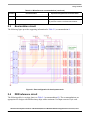
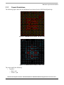
The i.MX 6Dual/6Quad processor comes in a 21 × 21 mm package with 0.8 mm ball pitch. The ball-grid
array contains 25 rows and 25 columns, making it a 624 ball BGA package. For detailed information
about the package, see the i.MX 6 series Consumer and Automotive datasheets.
The following figure shows the ball-grid array. Figure 3-2 shows additional package information.
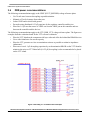
Figure 3-1. i.MX 6DQ/SDL ball-grid array
Hardware Development Guide for i.MX 6Dual/6Quad and i.MX 6Solo/6DualLite Applications Processors, Rev. 1
Freescale Semiconductor
3-1
i.MX 6 Series Layout Recommendations
Figure 3-2. i.MX 6DQ/6SDL package information
It is critical to maintain the recommended footprint of a 16 mils pad with a 20 mil open solder mask for
ease of fanout. In this case, the solder paste is the same as the pad with 16 mil, which allows an air gap of
15.496-mil between pads.
When using the Allegro tool, optimal practice is to use the footprint as created by Freescale. When not
using the Allegro tool, use the Allegro footprint export feature (supported by many tools). If export is not
possible, create the footprint as per the package mechanical dimensions outlined in the product data sheet.
Hardware Development Guide for i.MX 6Dual/6Quad and i.MX 6Solo/6DualLite Applications Processors, Rev. 1
3-2
Freescale Semiconductor
i.MX 6 Series Layout Recommendations
3.1.1
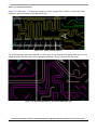
Fanout illustrations
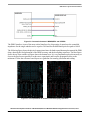
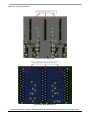
The following figures show the top and bottom layer fanouts for the i.MX 6Dual/6Quad chip.
Figure 3-3. i.MX6DQ fanout example, top layer view
Figure 3-4. i.MX6DQ fanout example, bottom view
The colors signify the following:
• Top layer
— Red = etch
— Yellow = pad
Hardware Development Guide for i.MX 6Dual/6Quad and i.MX 6Solo/6DualLite Applications Processors, Rev. 1
Freescale Semiconductor
3-3
i.MX 6 Series Layout Recommendations
•
3.1.2
— Gray = vias
Bottom layer
— Cyan = GND net
— Brown = power rails
Placing decoupling capacitors
The fanout scheme creates a four quadrant structure that facilitates the placement of decoupling bulk
capacitors on the bottom side of the PCB.
The 0201 decoupling and 0603 bulk capacitors should be mounted as close as possible to the power vias.
The distance should be less than 50 mils. Additional bulk capacitors can be placed near the edge of the
BGA via array. Placing the decoupling capacitors close to the power balls is critical to minimize inductance
and ensure high-speed transient current demand by the processor.
A correct via size is critical for preserving adequate routing space. The recommended geometry for the via
pads is: pad size 18 mils and drill 8 mils.
The following list provides the main recommendations for choosing the correct decoupling scheme for the
i.MX6 family boards.
• Place the largest capacitance in the smallest package that budget and manufacturing can support.
• For high speed bypassing, select the required capacitance with the smallest package (for example,
0.22 μF and package 0201).
• Minimize trace length (inductance) to small caps.
• Series inductance cancels out capacitance.
• Tie caps to GND plane directly with a via.
• Place capacitors close to the power contact of the associate package designed from the schematic.
The i.MX6 SABRE SD (Smart Devices) CPU uses the preferred BGA power decoupling design. Note that
the layout is available through www.freescale.com. Customers should use the reference design strategy for
power and decoupling.
3.2
Stackup recommendations
High-speed design requires a good stackup in order have the right impedance for the critical traces. The
constraints for the trace width may depend on a number of factors, such as the board stackup and associated
dielectric and copper thickness, required impedance, and required current (for power traces). The
Freescale reference design uses a minimum trace width of 3 mils for the DDR routing. The stackup also
determines the constraints for routing and spacing.
Consider the following when designing the stackup and selecting the material for your board.
• Board stack-up is critical for high-speed signal quality.
• You must preplan impedance of critical traces
• High-speed signals must have reference planes on adjacent layers to minimize cross-talk.
• FSL reference design equals Isola 370HR.
Hardware Development Guide for i.MX 6Dual/6Quad and i.MX 6Solo/6DualLite Applications Processors, Rev. 1
3-4
Freescale Semiconductor
i.MX 6 Series Layout Recommendations
•
FSL validation boards equals Isola FR408.
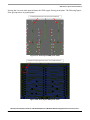
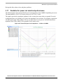
The recommended stackup is 8-layers, with the layer stack as shown in the following figure. The lefthand
image shows the detail provided by Freescale inside the fabrication detail as a part of the Gerber files. The
righthand side shows the solution suggested by the PCB fabrication company for our requirements.
Figure 3-5. Layer stack SABRE SD board
1
Additional power planes to support i.MX 6Dual/6Quad and i.MX 6Solo power options only.
The following table shows a working stack-up implementation:
Table 3-1. Stackup implementation
Single ended
Layers
Differential
Trace width Impedance Trace width Trace spacing Impedance Trace width Trace spacing Impedance
(Mils)
(Ωs)
(Mils)
‘Airgap’ (Mils)
(Ωs)
(Mils)
‘Airgap’ (Mils)
(Ωs)
TOP
4.7
50
4.3
5.7
90
3.7
5.3
INT1
4.5
50
4.2
5.8
90
3.8
5.2
INT2
4.5
50
4.2
5.8
90
3.8
5.2
BOT
4.7
50
4.3
5.7
90
3.7
5.3
100
100
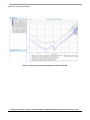
Figure 3-6. Example top layer impedance solution from PCB fabricator
Hardware Development Guide for i.MX 6Dual/6Quad and i.MX 6Solo/6DualLite Applications Processors, Rev. 1
Freescale Semiconductor
3-5
i.MX 6 Series Layout Recommendations
3.3
DDR connection information
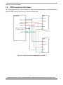
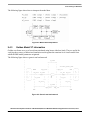
The following figures show the block diagrams from the reference design boards for the DDR3 interface
and the LPDDR2 interface (respectively) with the i.MX6DQ/SDL.
Figure 3-7. Connection between i.MX6DQ/SDL and DDR3
Hardware Development Guide for i.MX 6Dual/6Quad and i.MX 6Solo/6DualLite Applications Processors, Rev. 1
3-6
Freescale Semiconductor
i.MX 6 Series Layout Recommendations
Figure 3-8. Connection between i.MX6DQ/SDL and LPDDR2
The DDR3 interface is one of the most critical interfaces for chip routing. It must have the controlled
impedance for the single ended traces be equal to 50 Ω and for the differential pairs be equal to 100 Ω.
The following figure shows the physical connection scheme for both top and bottom placement of the DDR
chips, showing the final placement of the DDR3 memory and the decoupling capacitors. The blue figure
shows the top layer and the red figure shows the bottom layer. It is very important to place the memory as
close to the processor as possible to reduce trace capacitance and keep the propagation delay to the
minimum. Follow the reference board layout as a guideline for memory placement and routing.
Figure 3-9. Final placement of memories and decoupling capacitors
Hardware Development Guide for i.MX 6Dual/6Quad and i.MX 6Solo/6DualLite Applications Processors, Rev. 1
Freescale Semiconductor
3-7
i.MX 6 Series Layout Recommendations
3.4
DDR routing rules
DDR3 routing can be accomplished in two different ways: routing all signals at the same length or routing
by byte group.
Routing all signals at the same length can be more difficult at first because of the tight space between the
DDR and the processor and the large number of required interconnects. However, it is the better way
because it makes signal timing analysis straightforward. Ideally, we could route all the signals at the same
length, However, it could be difficult because of the large number of connections in the tight space between
the DDR and the processor. The following table explains the rules for routing the signals by the same
length.
Table 3-2. DDR3 routing by the same length
Signals
Total length
Recommendations
Address and Bank
Clock length
Data and Buffer
Clock length
Control signals
Clock length
Clock
DRAM_SDCLK[1:0]
Longest trace ≤ 3 inches
DRAM_SDQS[7:0] and
DRAM_SDQS[7:0]_B
Clock length
Match the signals ±25 mils of the value
specified in the length column
Match the signals of clocks signals
±5 mils. Each differential clock pair
Match the signals of DQS signals
±10 mils of the value specified in the
length column.
Routing by byte group requires better control of the signals of each group. It is also more difficult for
analysis and constraint settings. However, its advantage is that the constraint to match lengths can be
applied to a smaller group of signals. This is often more achievable once the constraints are properly set.
The following table explains the rules for routing the signals by byte group.
Table 3-3. DDR3 routing by byte group
Length
Chip signals
Group
Recommendations
Min
Max
DRAM_SDCLK[1:0]
DRAM_SDCLK_B[1:0]
Clock
Short as possible
2.25 inches
Match the signals ± 5 mils.
2.25 inches is recommended.
DRAM_A[15:0]
DRAM_SDBA[2:0]
DRAM_RAS DRAM_CAS
DRAM_SDWE
Address
and Command
Clock (min) – 200
Clock (min)1 Match the signals ± 25 mils.
Hardware Development Guide for i.MX 6Dual/6Quad and i.MX 6Solo/6DualLite Applications Processors, Rev. 1
3-8
Freescale Semiconductor
i.MX 6 Series Layout Recommendations
Table 3-3. DDR3 routing by byte group (continued)
Length
Chip signals
Group
Recommendations
Min
Max
DRAM_D[7:0]
DRAM_DQM0
DRAM_SDQS0
DRAM_SDQS0_B
Byte Group 1
—
Clock (min)
DRAM_D[15:8]
DRAM_DQM1
DRAM_SDQS1
DRAM_SDQS1_B
Byte Group 2
—
Clock (min)
DRAM_D[23:16]
DRAM_DQM2
DRAM_SDQS2
DRAM_SDQS2_B
Byte Group 3
—
Clock (min)
DRAM_D[31:24]
DRAM_DQM3
DRAM_SDQS3
DRAM_SDQS3_B
Byte Group 4
—
Clock (min)
DRAM_D[39:32]
DRAM_DQM4
DRAM_SDQS4
DRAM_SDQS4_B
Byte Group 5
—
Clock (min)
DRAM_D[47:40]
DRAM_DQM5
DRAM_SDQS5
DRAM_SDQS5_B
Byte Group 6
—
Clock (min)
DRAM_D[55:48]
DRAM_DQM6
DRAM_SDQS6
DRAM_SDQS6_B
Byte Group 7
—
Clock (min)
DRAM_D[63:56]
DRAM_DQM7
DRAM_SDQS7
DRAM_SDQS7_B
Byte Group 8
—
Clock (min)
DRAM_CS[1:0]
DRAM_SDCKE[1:0]
DRAM_SDODT[1:0]
Control signals
Clock (min) – 200
Clock (min)
Match the signals of each byte group ± 25
mils.
Match the differential signals of DQS ± 10
mils.
Match the signals ± 50 mils.
1. Clock (min)—The shortest length of the clock group signals because this group has a ± 5 mil matching tolerance.
Finally, the impedance for the signals should be 50 Ω for single ended and 100 Ω for differential pairs.
3.5
Routing considerations
The chip can handle up to 4 Gbytes of DRAM memory. i.MX6 DDR routing needs to be separated into
three groups: data, address, and control. Each group has its own method of routing from an i.MX 6
serieschip to DDR memory. The DDR layout has 2 Gbyte and 4 Gbyte options.
Hardware Development Guide for i.MX 6Dual/6Quad and i.MX 6Solo/6DualLite Applications Processors, Rev. 1
Freescale Semiconductor
3-9
i.MX 6 Series Layout Recommendations
3.5.1
Swapping data lines
The DDR3 pin swapping technique for the data bus lines within bytes makes it easier to:
• Route direct lines
• Avoid changes between layers
The rules are as follows:
• Hardware write leveling – lowest order bit within byte lane must remain on lowest order bit of lane
by JEDEC compliance (see the “Write Leveling” section in JESD79-3E)
— D0, D8, D16, D24, D32, D40, D48, and D56 are fixed
— Other data lines free to swap within byte lane
• JEDEC DDR3 memory restrictions are:
– No restrictions for complete byte lane swapping
– DQS and DQM must follow lanes
NOTE
If byte lane swapping was done, target DDR IC register read value must be
transposed according to the data line swapping.
3.5.2
DDR3 (64 bits) T topology considerations
Be sure to take into account the following when designing a T-topology system.
• Follow the routing rules described in Table 3-3.
• Termination resistors not required.
• Short routing lengths and on-chip drive strength control.
• Your design is limited to 4 DDR chips.
• DDR3, 2 GBytes using latest memories (4 GBytes coming).
3.5.3
DDR3 (64 bits) Fly-by topology considerations
Pay attention to the following recommendations when the Fly-by topology and routing technique.
• DDR controller provides address mirroring when using two chip selects, which aids address line
routing for memories on both sides of board.
• Bus termination resistors are required.
3.5.4
2-Gigabyte recommendations
The 2 Gbyte option has four memories. You should follow these recommendations for best practice:
• Have a balanced routing for the T connection.
• Avoid having many layer transitions.
• Do not cross split reference planes during the routing.
Hardware Development Guide for i.MX 6Dual/6Quad and i.MX 6Solo/6DualLite Applications Processors, Rev. 1
3-10
Freescale Semiconductor
i.MX 6 Series Layout Recommendations
The following figure shows the topology for the ADDR/CMD/CTRL signals. It has a tree topology. Note
the balanced T routing.
Figure 3-10. ADDR/CMD/CTRL signal topology
The routing for the data groups depends on the bus size. The following figure shows the point-to-point data
bus connection, with routing by byte group.
Figure 3-11. Point-to-point data bus connection (routing by byte group)
NOTE
i.MX 6Solo only uses the first two pairs of the 2 Bytes groups. All others are
disabled.
3.5.5
4-Gigabyte recommendations
The following diagrams show the 4 Gbyte recommendations using both chip selects (CS[1:0]) and loading
2 GBytes to each one. This option has eight memories and requires the addition of a termination resistor.
Hardware Development Guide for i.MX 6Dual/6Quad and i.MX 6Solo/6DualLite Applications Processors, Rev. 1
Freescale Semiconductor
3-11
i.MX 6 Series Layout Recommendations
Route the ADDR/CMD signals as shown in the following figure.
Figure 3-12. ADDR/CMD signal topology
Figure 3-13. CTRL signal topology
Figure 3-14. Data bus routing topology
Figure 3-15. Clock routing topology
Hardware Development Guide for i.MX 6Dual/6Quad and i.MX 6Solo/6DualLite Applications Processors, Rev. 1
3-12
Freescale Semiconductor
i.MX 6 Series Layout Recommendations
3.5.6
Four chips T topology routing examples
The figures in this section show examples for the routing of the 2 GByte DDR3 memories. Figure 3-16
through Figure 3-18 are a guideline of the T configuration routing with eight layers PCB.Table 3-4 shows
the color coding used in the figures.
Table 3-4. Color code
Color
Meaning
Soft Green
ADD & CMD Signals
Yellow
Clocks
Soft Pink
Data Byte Group 0
Purple
Data Byte Group 1
Blue
Data Byte Group 2
Brown
Data Byte Group 3
Orange
Data Byte Group 4
Green
Data Byte Group 5
Olive Green
Data Byte Group 6
Soft Brown
Data Byte Group 7
Gray
DDR_1V5 & DDR_VREF
Soft Red
Control Signals
Hardware Development Guide for i.MX 6Dual/6Quad and i.MX 6Solo/6DualLite Applications Processors, Rev. 1
Freescale Semiconductor
3-13
i.MX 6 Series Layout Recommendations
Figure 3-16. Top layer DDR3 routing
Hardware Development Guide for i.MX 6Dual/6Quad and i.MX 6Solo/6DualLite Applications Processors, Rev. 1
3-14
Freescale Semiconductor
i.MX 6 Series Layout Recommendations
Figure 3-17. Internal L6 DDR3 routing
Hardware Development Guide for i.MX 6Dual/6Quad and i.MX 6Solo/6DualLite Applications Processors, Rev. 1
Freescale Semiconductor
3-15
i.MX 6 Series Layout Recommendations
Figure 3-18. Bottom layer DDR3 routing
The following table shows the total etch of the signals for the byte 0 and byte 1 groups. The layout is an
example, using 2000 mils for the clock.
Table 3-5. Total signal etch (DDR3)
Signals
Length (Mils)
DRAM_D0
1025.349
DRAM_D1
1028.996
DRAM_D2
1028.752
DRAM_D3
1021.158
DRAM_D4
1021.930
DRAM_D5
1025.398
DRAM_D6
1025.564
DRAM_D7
1029.326
Hardware Development Guide for i.MX 6Dual/6Quad and i.MX 6Solo/6DualLite Applications Processors, Rev. 1
3-16
Freescale Semiconductor
i.MX 6 Series Layout Recommendations
Table 3-5. Total signal etch (DDR3) (continued)
3.5.7
Signals
Length (Mils)
DRAM_DQM0
1028.555
DRAM_SDQS0
1023.419
DRAM_SDQS0_B
1023.373
DRAM_D8
648.862
DRAM_D9
654.371
DRAM_D10
652.653
DRAM_D11
653.712
DRAM_D12
650.961
DRAM_D13
648.433
DRAM_D14
649.588
DRAM_D15
651.781
DRAM_DQM1
653.106
DRAM_SDQS1
669.240
DRAM_SDQS1_B
669.736
DRAM_SDCLK0
2120.044
DRAM_SDCLK0_B
2118.283
DRAM_SDCLK1
2112.518
DRAM_SDCLK1_B
2112.829
Eight chips fly-by topology routing examples
The figures in this section show examples for the routing of 4-Gbyte DDR memories. These figures are a
guideline of the routing by layer using the fly by configuration topology. They use the same color code
shown in Table 3-4.
NOTE
The SABRE SD board referenced in the beginning of this chapter does not
use eight DDR chips. The following screen shots are from the validation
board layout.
Hardware Development Guide for i.MX 6Dual/6Quad and i.MX 6Solo/6DualLite Applications Processors, Rev. 1
Freescale Semiconductor
3-17
i.MX 6 Series Layout Recommendations
Figure 3-19. Top DDR3 routing
Hardware Development Guide for i.MX 6Dual/6Quad and i.MX 6Solo/6DualLite Applications Processors, Rev. 1
3-18
Freescale Semiconductor
i.MX 6 Series Layout Recommendations
Figure 3-20. Internal L3 DDR3 routing
Hardware Development Guide for i.MX 6Dual/6Quad and i.MX 6Solo/6DualLite Applications Processors, Rev. 1
Freescale Semiconductor
3-19
i.MX 6 Series Layout Recommendations
Figure 3-21. Internal L4 DDR3 routing
Hardware Development Guide for i.MX 6Dual/6Quad and i.MX 6Solo/6DualLite Applications Processors, Rev. 1
3-20
Freescale Semiconductor
i.MX 6 Series Layout Recommendations
Figure 3-22. Internal L11 DDR3 routing
Hardware Development Guide for i.MX 6Dual/6Quad and i.MX 6Solo/6DualLite Applications Processors, Rev. 1
Freescale Semiconductor
3-21
i.MX 6 Series Layout Recommendations
Figure 3-23. Internal L12 DDR3 routing
Hardware Development Guide for i.MX 6Dual/6Quad and i.MX 6Solo/6DualLite Applications Processors, Rev. 1
3-22
Freescale Semiconductor
i.MX 6 Series Layout Recommendations
Figure 3-24. Bottom DDR3 routing
Hardware Development Guide for i.MX 6Dual/6Quad and i.MX 6Solo/6DualLite Applications Processors, Rev. 1
Freescale Semiconductor
3-23
i.MX 6 Series Layout Recommendations
The following table shows the total etch of the signals for the byte 0 and byte 1 groups.
Table 3-6. Total signal etch (DDR3)
Signals
Length (Mils)
DRAM_D0
1244.97
DRAM_D1
1252.82
DRAM_D2
1237.48
DRAM_D3
1242.95
DRAM_D4
1240.12
DRAM_D5
1254.37
DRAM_D6
1254.58
DRAM_D7
1238.18
DRAM_DQM0
1297.45
DRAM_SDQS0
1295.34
DRAM_SDQS0_B
1295.68
DRAM_D8
1103.69
DRAM_D9
1116.14
DRAM_D10
1105.01
DRAM_D11
1105.17
DRAM_D12
1120.4
DRAM_D13
1123.06
DRAM_D14
1105.72
DRAM_D15
1111.24
DRAM_DQM1
1152.16
DRAM_SDQS1
1158.48
DRAM_SDQS1_B
1162.29
DRAM_SDCLK0
4723.96
DRAM_SDCLK0_B
4681.95
DRAM_SDCLK1
4750.69
DRAM_SDCLK1_B
4699.00
Hardware Development Guide for i.MX 6Dual/6Quad and i.MX 6Solo/6DualLite Applications Processors, Rev. 1
3-24
Freescale Semiconductor
i.MX 6 Series Layout Recommendations
3.5.8
High speed signal routing recommendations
The following list provides recommendations for routing traces for high speed signals. Note that the
propagation delay and the impedance control should match in order to have the correct communication
with the devices.
• High-speed signals (DDR, RGMII, display) must not cross gaps in the reference plane.
• Avoid creating slots, voids, and splits in reference planes. Review via voids to ensure they do not
create splits (space out vias).
• A solid GND plane must be directly under crystal, associated components, and traces.
• Clocks or strobes that are on the same layer need at least 2.5× spacing from an adjacent trace (2.5×
height from reference plane) to reduce cross-talk.
• All synchronous modules should have bus length matching and relative clock length control.
— For SD module interfaces:
– Match data and CMD trace lengths (length delta depends on bus rates)
– CLK should be longer than the longest signal in the Data/CMD group (+5 mils)
— Similar DDR rules must be followed for data, address and control as for SD module interfaces.
3.5.9
Ground plane recommendations
This section provides examples of good practices and how to avoid common user mistakes when flowing
the ground planes layers.
The following two figures show common examples of poor GND planes. The copper plane is represented
by the color gray in Figure 3-25 and by the horizontal green lines in Figure 3-26.
Hardware Development Guide for i.MX 6Dual/6Quad and i.MX 6Solo/6DualLite Applications Processors, Rev. 1
Freescale Semiconductor
3-25
i.MX 6 Series Layout Recommendations
Figure 3-25. Poor GND plane 1
Figure 3-26. Poor GND plane 2
Hardware Development Guide for i.MX 6Dual/6Quad and i.MX 6Solo/6DualLite Applications Processors, Rev. 1
3-26
Freescale Semiconductor
i.MX 6 Series Layout Recommendations
Spacing the vias some mils apart facilitates the GND copper flowing in the plane. The following figures
show good practices of ground planes.
Figure 3-27. Good layout GND plane detail
Figure 3-28. Good layout GND plane detail
Hardware Development Guide for i.MX 6Dual/6Quad and i.MX 6Solo/6DualLite Applications Processors, Rev. 1
Freescale Semiconductor
3-27
i.MX 6 Series Layout Recommendations
3.6
DDR power recommendations
The following recommendations apply to the VREF (P0V75_REFDDR) voltage reference plane.
• Use 30 mils trace between decoupling cap and destination.
• Maintain a 25 mils clearance from other nets.
• Isolate VREF and/or shield with ground.
• Decouple using distributed 0.22 μF capacitors by the regulator, controller, and devices.
• Place one 1.0 μF near the source of VREF: one near the VREF pin on the controller and two
between the controller and the devices.
The following recommendations apply to the VTT (DDR_VTT) voltage reference plane. The figures are
examples from the evaluation board for the VTT reference schematic.
• Place the VTT island on the component side layer at the end of the bus behind the DRAM devices.
• Use a wide-island trace for current capacity.
• Place the VTT generator as close to termination resistors as possible to minimize impedance
(inductance).
• Place one or two 0.1 μF decoupling capacitors by each termination RPACK on the VTT island to
minimize the noise on VTT. Other bulk (10–22 pF) decoupling is also recommended to be placed
on the VTT island.
Figure 3-29. DDR_VTT evaluation board example
Hardware Development Guide for i.MX 6Dual/6Quad and i.MX 6Solo/6DualLite Applications Processors, Rev. 1
3-28
Freescale Semiconductor
i.MX 6 Series Layout Recommendations
Figure 3-30. DDR_VTT evaluation board examples
3.7
PCI Express interface recommendations
This chip provides a ×1 PCIe lane. The PCIe module supports PCI Express Gen 2.0 interfaces at 5 Gb/s.
It is also backwards compatible to Gen 1.1 interfaces at 2.5 Gb/s.
NOTE
Lane ×1 is composed of two differential signals pairs: one TXD signal pair
and one RXD signal pair.
Table 3-7. PCI Express signal descriptions
3.7.1
Signal name
Signal group
Description
PCIE_TXP, PCIE_TXM
Data
PCI Express transmit differential pair
PCIE_RXP, PCIE_RXM
Data
PCI Express receive differential pair
PCI Express general routing guidelines
Use the following recommendations for PCI Express general routing:
• The trace width and spacing of the lanes ×1 signals should be such that the differential impedance
is 85 Ω ± 10%.
• The PCIE_REXT contacts should be connected to a 200 Ω 1% resistor to ground. The trace length
between the pin and the resistor should be minimized. The resistor value is defined within the data
sheet and should determine the exact resistor value.
• Route traces over continuous planes (power and ground). Avoid split planes, plane slots, or
anti-etch.
• Maintain the parallelism (skew matched) between differential signals; these traces should be the
same overall length.
• Keep signals with traces as short as possible.
• Route signals with a minimum amount of corners. Use 45-degree turns instead of 90-degree turns.
• Do not create stubs or branches.
• Maintain symmetry of differential pair routing.
Hardware Development Guide for i.MX 6Dual/6Quad and i.MX 6Solo/6DualLite Applications Processors, Rev. 1
Freescale Semiconductor
3-29
i.MX 6 Series Layout Recommendations
3.7.2
PCI Express coupling lane
Based on our development design, we have the following coupling signal schema. Consult the PCISig
documentation for detailed information.
• DC-coupled Rx signals with 0 Ω resistors
• AC-coupled Tx signals with 0.1µF capacitors
3.7.3
Additional resources for PCI Express signal routing
recommendations
For more information about, PCI Express signal routing recommendations, see the following.
• Freescale Hardware Design Considerations for PCI Express® and SGMII
(http://www.freescale.com/files/training_presentation/TP_HARDWARE_DESIGN_PCI_SMGIII
.pdf)
• PCISig, PCI Express Base Specification.
• PCISig, PCI Express Card Electromechanical Specification.
• PCISig, PCSIG Board Design Guidelines for PCI Express™ Architecture.
• PCI Express Basics: Developing Physical Design Rules for PCIe
(http://www.mentor.com/products/pcb-system-design/multimedia/pcie-basics-webinar)
3.8
HDMI recommendations
Use the following recommendations for the HDMI.
• HDMI differential pairs should have a impedance of 100 Ω in all paths to the connector.
• It is highly recommended to use an HDMI transmitter port protection for ESD, level shifting,
isolation, overcurrent and backdrive protecion.
3.9
SATA recommendations
Use the following recommendations for the SATA.
• SATA differential pairs should have a differential impedance of 100 Ω.
• Each differential pair should be length matched to ± 5 mils.
• Follow standard high-speed differential routing rules for signal integrity.
3.10
LVDS recommendations
Use the following recommendations for the LVDS.
• Follow standard high-speed differential routing rules for signal integrity.
• Each differential pair should be length matched to ± 5 mils.
• LVDS differential pairs should have a differential impedance of 100 Ω.
Hardware Development Guide for i.MX 6Dual/6Quad and i.MX 6Solo/6DualLite Applications Processors, Rev. 1
3-30
Freescale Semiconductor
i.MX 6 Series Layout Recommendations
3.11
USB recommendations
Use the following recommendations for the USB.
• Route the high speed clocks and the DP and DM differential pair first.
• Route DP and DM signals on the top or bottom layer of the board
• The trace width and spacing of the DP and DM signals should be such that the differential
impedance is 90 Ω.
• Route traces over continuous planes (power and ground).
— They should not pass over any power/GND plane slots or anti-etch.
— When placing connectors, make sure the ground plane clearouts around each pin have ground
continuity between all pins.
• Maintain the parallelism (skew matched) between DP and DM; these traces should be the same
overall length.
• Do not route DP and DM traces under oscillators or parallel to clock traces and/or data buses.
• Minimize the lengths of high speed signals that run parallel to the DP and DM pair.
• Keep DP and DM traces as short as possible.
• Route DP and DM signals with a minimum amount of corners. Use 45-degree turns instead of
90-degree turns.
• Avoid layer changes (vias) on DP and DM signals. Do not create stubs or branches.
3.12
Impedance signal recommendations
Use the following table as a reference when you are updating or creating constraints in your software PCB
tool to set up the impedance and the correct trace width.
Table 3-8. Impedance signal recommendations
Impedance
Layout
Tolerance (±)
All signals, unless specified
50 Ω SE
10%
PCIe Diff signals
85 Ω Diff
10%
USB Diff signals
90 Ω Diff
10%
Diff signals:
LVDS, SATA, HDMI, DDR, MIPI (CSI & DSI), MLB, Phy IC to Ethernet
Connector
100 Ω Diff
10%
Signal Group
Hardware Development Guide for i.MX 6Dual/6Quad and i.MX 6Solo/6DualLite Applications Processors, Rev. 1
Freescale Semiconductor
3-31
i.MX 6 Series Layout Recommendations
The following figure shows the dimensions of a stripline and microstrip pair. Figure 3-32 shows the
differential pair routing.
Figure 3-31. Microstrip and stripline differential pair dimensions
Figure 3-32. Differential pair routing
•
•
3.13
The space between two adjacent differential pairs should be greater than or equal to twice the space
between the two individual conductors.
The skew between LVDS pairs should be within the minimum recommendation (± 100 mil).
Reference resistors
NOTE
The reference resistor and the connection should be placed away from noisy
regions. Noise induced on it may impact the internal circuit and degrade the
interface signals.
Hardware Development Guide for i.MX 6Dual/6Quad and i.MX 6Solo/6DualLite Applications Processors, Rev. 1
3-32
Freescale Semiconductor
i.MX 6 Series Layout Recommendations
3.14
ESD and radiated emissions recommendations
The PCB design should use six or more layers, with solid power and ground planes. The recommendations
for ESD immunity and radiated emissions performance are as follows:
• All components with ground chassis shields (USB jack, buttons, and so forth) should connect the
shield to the PCB chassis ground ring.
• Ferrite beads should be placed on each signal line connecting to an external cable. These ferrite
beads must be placed as close to the PCB jack as possible.
NOTE
Ferrite beads should have a minimum impedance of 500 Ω at 100 MHz with
the exception of the ferrite on USB_5V.
•
•
•
3.15
Ferrite beads should NOT be placed on the USB D+/D– signal lines as this can cause USB signal
integrity problems. For radiated emissions problems due to USB, a common mode choke may be
placed on the D+/D– signal lines. However, in most cases, it should not be required if the PCB
layout is satisfactory. Ideally, the common mode choke should be approved for high speed USB use
or tested thoroughly to verify there are no signal integrity issues created.
It is highly recommended that ESD protection devices be used on ports connecting to external
connectors. See the reference schematic (available at www.freescale.com) for detailed information
about ESD protection implementation on the USB interfaces.
If possible, stitch all around the board with vias with 100 mils spacing between them connected to
GND planes with exposed solder mask to improve EMI.
Component placement recommendations
Adhere to the following recommendations when placing components.
• Place components such that short and/or critical routes can be easily laid out.
— Critical routes determine component location.
— Orient devices to facilitate routes (minimize length and crossovers).
• Consider placing the following pairings adjacent.
— i.MX and DDR
— PHY and associated jack
— Jack and CODEC input
— Bluetooth® (or other RF) and antenna
3.16
Reducing skew and phase problems in deferential pairs traces
Differential pair technology has evolved to require more stringent checking in the area of phase control.
This is evident on the higher data rates associated with parallel buses such as PCI Gen 2, DDR, LVDS, or
Ethernet. In the simplest of terms, Diff Pair technology sends opposite and equal signals down a pair of
traces. Keeping these opposite signals in phase is essential to assuring that they function as intended.
Hardware Development Guide for i.MX 6Dual/6Quad and i.MX 6Solo/6DualLite Applications Processors, Rev. 1
Freescale Semiconductor
3-33
i.MX 6 Series Layout Recommendations
Figure 3-33 and Figure 3-34 show two examples of static routing where a match is achieved without
needing to tune one element of the differential pair.
Figure 3-33. Yellow traces diff pairs 1
The following figure shows the addition of a delay trace to one element of the differential pair to avoid
length mismatch (which reduces skew and phase problems). The green box marks the detail.
Figure 3-34. Small bumps added to the shorter differential pair
Hardware Development Guide for i.MX 6Dual/6Quad and i.MX 6Solo/6DualLite Applications Processors, Rev. 1
3-34
Freescale Semiconductor
i.MX 6 Series Layout Recommendations
Having this delay reduces skew and phase problems.
3.17
Guideline for power net electrical performance
The following figure shows the simulated open-circuit impedance of the SABRE AI platform power nets.
The board number is 700-27142, layout version is LAY-27142_C-1004.
The graph is provided as impedance guidance for the various power nets relative to ground. Freescale
recommends that a user’s board be at or below the impedances curves shown. For example, consider the
100 MHz point on the VDD_ARM_CAP curve at 0.065 ohms. User layouts at 100 MHz should have
impedance from VDD_ARM_CAP to ground of 0.065 ohms or less.
Figure 3-35. Power Net Open-Circuit Impedance – 10 kHz to 100 MHz
Hardware Development Guide for i.MX 6Dual/6Quad and i.MX 6Solo/6DualLite Applications Processors, Rev. 1
Freescale Semiconductor
3-35
i.MX 6 Series Layout Recommendations
Figure 3-36. Power net open-circuit impedance-10 kHz to 10 GHz
Hardware Development Guide for i.MX 6Dual/6Quad and i.MX 6Solo/6DualLite Applications Processors, Rev. 1
3-36
Freescale Semiconductor
Chapter 4
Requirements for Power Management
4.1
Power management requirements overview
This chapter provides the power requirements for the following i.MX 6 series families of processors:
• i.MX 6Quad
• i.MX 6Dual
• i.MX 6DualLite
• i.MX 6Solo
4.1.1
Voltage domains overview
These chips have several voltage domains that may need to be supplied with different voltages depending
on system needs. The chip internal regulators and its complementary PMIC PF0100 provide a complete
and simple way to supply each voltage domain with different voltages when needed. Section 4.4,
“Connection diagrams,” shows the internal regulators and the connections to PF0100.
4.1.2
PF0100 overview
PF0100 consists of the following components used to supply the i.MX6 voltage domains as well as other
blocks on the system:
• 4 buck regulators
• 1 boost regulator
• 8 LDOs
The default PF0100 power-up sequence is programmed to fit the requirements of the i.MX 6 series families
of processors. However, the PF0100 can be adjusted to meet the specific requirements for system
applications by using the one time programmable (OTP) feature.
4.2
Requirements for a generic interface between chip and PF0100
Table 4-1 shows the generic interface between the chip and PF0100, using a suitable power-up sequence.
For more info about PF0100 functionality and the i.MX 6 series families of processors’ power
requirements, see the product data sheets.
Hardware Development Guide for i.MX 6Dual/6Quad and i.MX 6Solo/6DualLite Applications Processors, Rev. 1
Freescale Semiconductor
4-1
Requirements for Power Management
Table 4-1. Interface between the chip and PF0100
Voltage rail
Supply reg
Voltage
(V)
Supply
reg
current
capability
(A)
VDDARM_IN
SW1A/B
1.35
2.5
PF0100
1
Short these together with a shunt
for quad core operation. Cut shunt
for dual core operation and connect
VDDARM23_IN to GND
Note 1
(1.2)
—
i.MX
—
Short these together with a shunt
for quad core operation. Cut shunt
for dual core operation and connect
VDDARM23_IN to GND
VDDSOC_IN
SW1C
1.325
2.0
PF0100
1
VDDARM_IN and VDDSOC_IN
supplies can be shorted together
and run off of one fewer switcher
for cost-sensitive platforms.
VDDSOC_CAP
Note 1
(1.1)
—
i.MX
VDDPU_CAP
Note 1
(1.2)
—
i.MX
—
—
VDDHIGH_IN
SW2
3.0
2.0
PF0100
2
—
VDDHIGH_CAP
Note 1
(2.5)
—
i.MX
VDD_SNVS_IN
VSNVS
3.0
400 μA
PF0100
0
According to table 13 of the chip
data sheet, VDD_SNVS_IN can
draw up to 1 mA depending on the
application. For those cases, an
external regulator is needed
because the PF0100 VSNVS
regulator supplies 400 μA.
NVCC_RGMII
SW3A/B
1.5
1.25
PF0100
3
—
Generated
by
Power up
sequence
VDDARM23_IN
VDDARM_CAP
VDDARM23_CAP
Short these together.
VDDSOC_CAP is the output of an
i.MX6 internal LDO that can supply
more voltage domains as indicated
below in this table.
VDD_CACHE_CAP
VDDHIGH_CAP is the output of an
i.MX6 internal LDO that can supply
more voltage domains as indicated
below in this table.
NVCC_DRAM
DRAM_VREF
Notes
SW3 can be configured from 0.4 to
3.3 V so that the right voltage can
be chosen for the respective DDR
technology.
VREFDDR or
SW4
0.5×SW3 0.01 or 1.0
PF0100
3
—
Hardware Development Guide for i.MX 6Dual/6Quad and i.MX 6Solo/6DualLite Applications Processors, Rev. 1
4-2
Freescale Semiconductor
Requirements for Power Management
Table 4-1. Interface between the chip and PF0100 (continued)
Voltage rail
Supply reg
NVCC_CSI
SW4, VGEN4 or
external
NVCC_EIM 0, 1, 21
regulator
Voltage
(V)
Supply
reg
current
capability
(A)
1.8–3.3
Generated
by
Power up
sequence
1.0 or 0.35
PF0100 or
external
regulator
5
Depending on system needs, these
voltage domains can be supplied
together or independently with
equal or different voltages and
regulators. Be sure to account for
the current needs of the domains
and the current capability of the
regulator when making this
decision.
NVCC_ENET
NVCC_GPIO
NVCC_LCD
NVCC_NANDF
Notes
NVCC_SD1, 2
NVCC_SD3
NVCC_JTAG
NVCC_PLL_OUT
Note 2
1.1
—
i.MX
—
—
NVCC_MIPI
VDDHIGH_CAP
2.5
—
i.MX
—
—
NVCC_LVDS2P5
VDDHIGH_CAP
2.5
—
i.MX
—
This supply also powers the
pre-drivers of the DDR IO pins.
Therefore, it must always be
provided, even when LVDS is not
used.
USB_OTG_VBUS
SWBST
5.0
0.6
PF0100
—
• In Host configuration,
USB_OTG_VBUS can be fed
from the SWBST output of the
PF0100.
• In device configuration,
USB_OTG_VBUS is the
external host that provides this
voltage.
USB_H1_VBUS
SWBST
5.0
0.6
PF0100
—
Connect to VBUS pin of USB
connector
VDDUSB_CAP
Note 2
(3.0)
—
i.MX
—
—
SATA_VP
VDDSOC_CAP
1.1
—
i.MX
—
—
SATA_VPH
VDDHIGH_CAP
2.5
—
i.MX
—
—
HDMI_VP
VDDSOC_CAP
1.1
—
i.MX
—
—
HDMI_VPH
VDDHIGH_CAP
2.5
—
i.MX
—
—
PCIE_VP
VDDSOC_CAP
1.1
—
i.MX
—
—
—
—
PCIE_VPTX
—
Hardware Development Guide for i.MX 6Dual/6Quad and i.MX 6Solo/6DualLite Applications Processors, Rev. 1
Freescale Semiconductor
4-3
Requirements for Power Management
Table 4-1. Interface between the chip and PF0100 (continued)
Voltage rail
Supply reg
Voltage
(V)
Supply
reg
current
capability
(A)
PCIE_VPH
VDDHIGH_CAP
2.5
—
Generated
by
Power up
sequence
i.MX
—
Notes
—
1 For Solo and DualLite chips, these 3 voltage rails should be connected together to the same voltage value.
Quad and Dual chips can support three different EIM power rails.
2 These voltage domains are supplied by i.MX6 internal regulators.
3 VGEN6, which comes up in sequence 4, does not power any i.MX rails and therefore is not shown. See Table 4-2 for VGEN6.
The following table shows the PF0100 regulators that are available to supply the rest of the system
circuitry.
Table 4-2. PF0100 regulators for other system circuitry
Supply
Output voltage(V)
Step size (mV)
Maximum Load current (mA)
SW41
0.5 × SW3A_OUT, 0.4 – 3.3
25/50
1000
VGEN1
0.75 – 1.5
50
100
VGEN2
0.75 – 1.5
50
250
VGEN3
1.8 – 3.3
100
100
VGEN41
1.8 – 3.3
100
350
VGEN5
1.8 – 3.3
100
100
VGEN6
1.8 – 3.3
100
200
1 In Table 4-1, it was recommended to supply the NVCC_x voltage domains with SW4 or VGEN4. Depending on the decision,
one of them may not be available to supply the rest of the system circuitry.
4.3
i.MX6 internal regulators
These chips have been equipped with 7 internal regulators that simplify the power supply scheme of the
system. The following table shows the regulators’ power requirements. See Section 4.4, “Connection
diagrams,” for the distribution and connections of these LDOs.
Table 4-3. Internal regulator power requirements
LDO
Output voltage (V)
Output current (mA)
LDO_ARM
1.1
—
LDO_SOC
1.2
—
LDO_PU
1.1
—
Hardware Development Guide for i.MX 6Dual/6Quad and i.MX 6Solo/6DualLite Applications Processors, Rev. 1
4-4
Freescale Semiconductor
Requirements for Power Management
Table 4-3. Internal regulator power requirements (continued)
LDO
Output voltage (V)
Output current (mA)
LDO_2P5
2.5
350
LDO_1P1
1.1
—
LDO_SNVS
1.1
—
LDO_USB
3.0
50
Hardware Development Guide for i.MX 6Dual/6Quad and i.MX 6Solo/6DualLite Applications Processors, Rev. 1
Freescale Semiconductor
4-5
Requirements for Power Management
4.4
Connection diagrams
Figure 4-1. i.MX6x/PF0100 connection diagram, 1 of 2
Hardware Development Guide for i.MX 6Dual/6Quad and i.MX 6Solo/6DualLite Applications Processors, Rev. 1
4-6
Freescale Semiconductor
Requirements for Power Management
1
Choose the pullup voltage for the I2C lines based on the I2C channel chosen. For example, for the I2C3 channel,
the corresponding voltage domain is NVCC_GPIO.
Figure 4-2. i.MX6x/PF0100 connection diagram, 2 of 2
Hardware Development Guide for i.MX 6Dual/6Quad and i.MX 6Solo/6DualLite Applications Processors, Rev. 1
Freescale Semiconductor
4-7
Requirements for Power Management
4.5
Video power recommendations
VDD_PU_CAP is the supply for the internal video processing units (VPU). For video intensive operations,
the VPU requires a lot of power and may undergo large swings of instantaneous current requirements.
Therefore, the power supply to the VPU must be designed to handle relatively large surges of current at
high frequencies from the original source to the processor input for power (VDD_SOC_IN) and at the
output of the internal regulator for VPU operations (VDD_PU_CAP). The following list provides
recommendations for each specific point along the current supply path. It may be necessary to implement
all of these recommendations to ensure that one particular point along the supply path does not become a
current choke point.
• The voltage with which VDD_SOC_IN will be fed must have a maximum tolerance of ± 25 mV.
PF0100's SW1C is already designed with this tolerance. Care must be taken if the design uses a
different regulator.
• VDD_SOC_CAP and VDD_PU_CAP bulk capacitance must be equal to 22 μF so that start up
current through the on board LDOs is reduced.
• These bulk capacitors must be very close to the VDD_SOC_CAP and VDD_PU_CAP pins
respectively and the connecting traces must be as thick as the design allows so the ability of being
a bulk capacitor for high speed operations is not limited.
• VDD_SOC_IN requires 66 μF of bulk capacitance because it supplies power for both
VDD_SOC_CAP and VDD_PU_CAP.
Hardware Development Guide for i.MX 6Dual/6Quad and i.MX 6Solo/6DualLite Applications Processors, Rev. 1
4-8
Freescale Semiconductor
Chapter 5
Using the Clock Connectivity Table
This chapter provides a reference table of the root clock default speed and a list of the i.MX modules
available to exit stop mode.
5.1
Root clocks
Clock connectivity is described in the “System Clocks Connectivity” section in the CCM chapter of the chip
reference manual. This section contains a series of tables that describe the clock inputs of each module and
which clock is connected to it.
NOTE
In some cases, a clock is associated with an external interface and is sourced
from a pad (mainly through IOMUX) and not from the CCM. Such clocks do
not appear in the clock connectivity table. They are found in the “External
Signals and Pin Multiplexing” chapter.
Clock gating is done with the low power clock gating (LPCG) module based on a combination of the clock
enable signals. For information about how the clock gating signals are logically combined, see the LPCG
section in the CCM chapter of the chip reference manual.
Table 5-1 lists the available clock sources and the default frequencies that are configured by design. In
some cases, users need to divide the clock inside the module when the maximum frequency is used in order
to meet the protocol requirements. CCM (the clock controller module) generates and drives the clock
sources.
For information about how the root clocks are generated, see the clock generation diagrams in the CCM
chapter of the chip reference manual.
Table 5-1. Clock roots
Clock Root Name (from CCM)
Description
Default frequency [MHz]
ARM_CLK_ROOT
ARM core clock
792
MMDC_CH0_CLK_ROOT
Multi Mode DDR Controller
528
AHB_CLK_ROOT
AMBA Bus
132
IPG_CLK_ROOT
Inter-packet Gap
66
PERCLK_CLK_ROOT
66
Hardware Development Guide for i.MX 6Dual/6Quad and i.MX 6Solo/6DualLite Applications Processors, Rev. 1
Freescale Semiconductor
5-1
Using the Clock Connectivity Table
Table 5-1. Clock roots (continued)
Clock Root Name (from CCM)
USDHC1_CLK_ROOT
Description
Ultra Secured Digital Host
Controller
Default frequency [MHz]
198
USDHC2_CLK_ROOT
198
USDHC3_CLK_ROOT
198
USDCH4_CLK_ROOT
198
SSI1_CLK_ROOT
Synchronous Serial Interface
63.525
SSI2_CLK_ROOT
63.525
SSI3_CLK_ROOT
63.525
GPU2D_AXI_CLK_ROOT
2D Graphics Processing Unit
GPU3D_AXI_CLK_ROOT
270
270
PCIE_AXI_CLK_ROOT
PCI Express
270
VDO_AXI_CLK_ROOT
Video Data Order Adapter
270
AXI_CLK_ROOT
Advanced eXtensible
Interface
270
IPU1_HSP_CLK_ROOT
IPU High-Speed
Processing Clock
264
IPU2_HSP_CLK_ROOT
5.2
264
Waking the core up from stop mode
The following modules can wake the core up from stop mode.
• CAN
• ECSPI
• EIM
• ENET
• EPIT
• GPC
• GPIO
• GPT
• I2C
• KPP
• PCIE
• SDMA
• UART
Hardware Development Guide for i.MX 6Dual/6Quad and i.MX 6Solo/6DualLite Applications Processors, Rev. 1
5-2
Freescale Semiconductor
Using the Clock Connectivity Table
•
USB
Hardware Development Guide for i.MX 6Dual/6Quad and i.MX 6Solo/6DualLite Applications Processors, Rev. 1
Freescale Semiconductor
5-3
Using the Clock Connectivity Table
Hardware Development Guide for i.MX 6Dual/6Quad and i.MX 6Solo/6DualLite Applications Processors, Rev. 1
5-4
Freescale Semiconductor
Chapter 6
Using the IOMUX Design Aid
This chapter provides users with the basic information required to use the IOMUX system design aid
(IOMux.exe). The IOMUX design aid facilitates the assignment of internal signals to external device
balls/pins by helping users:
• Record signal assignments for the supported i.MX device
• Identify conflicts, allowing them to be resolved in real time
• Add notes or comments for each signal to the list of recorded assignments
• Generate C code to configure the IOMUXC registers according to the user’s design
• Move signals to different modules to order configuration code into logical functions
Users can save design configurations for future use and/or export them for use in schematics or software
source code as supplementary documentation of a system.
The following figure shows a screenshot of the IOMUX application window with various areas labeled.
Figure 6-1. IOMUX tool for the i.MX6 families of applications processors
Hardware Development Guide for i.MX 6Dual/6Quad and i.MX 6Solo/6DualLite Applications Processors, Rev. 1
Freescale Semiconductor
6-1
Using the IOMUX Design Aid
6.1
Compatibility across the i.MX 6 series families of processors
The IOMUX registers for the i.MX 6 series families of processors are compatible as follows:
• The i.MX 6Quad family is compatible with the i.MX 6Dual family.
• i.MX 6DualLite family is compatible with the i.MX 6Solo family.
• i.MX 6Quad/6Dual families are not software compatible with i.MX 6DualLite/6Solo families.
Therefore, you cannot use code generated for i.MX 6Quad/6Dual for i.MX 6DualLite/6Solo and vice
versa.
6.2
Application requirements
The IOMUX application requires that the following be installed:
• Microsoft Windows XP or newer
• Microsoft’s .NET Framework, .NET Framework to 4.0 or newer.
6.3
IOMUX tool version
The IOMUX application i.MX 6Quad_6Dual IOMux Tool v3.2.1 supports the following devices in all
available package variations:
• i.MX 6Dual
• i.MX 6Quad
• i.MX 6Solo
• i.MX 6DualLite
6.4
IOMUX tool location
To obtain the IOMUX tool for the chip, consult your Freescale sales representative or download the
IOMUX tool from www.freescale.com.
Note that the IOMUX tool must be version v3.3 or later.
6.5
Learning to use the IOMUX tool
Consult the IOMUX user’s manual file inside the package for a detailed walkthrough of how to use the
IOMUX tool.
Hardware Development Guide for i.MX 6Dual/6Quad and i.MX 6Solo/6DualLite Applications Processors, Rev. 1
6-2
Freescale Semiconductor
Chapter 7
Configuring JTAG Tools
This chapter explains how to configure JTAG tools for debugging. The JTAG module is a standard JEDEC
debug peripheral. It provides debug access to important hardware blocks, such as the ARM® processor
and the system bus, which can give users access and control over the entire chip.
To prevent JTAG manipulation while allowing access for manufacturing tests and software debugging, the
i.MX 6 series processor incorporates a secure JTAG controller for regulating JTAG access. The secure
JTAG controller provides four different JTAG security modes, which are selected by e-Fuse configuration.
For more information about the security modes, see the “Security” section in the “System JTAG Controller
(SJC)” chapter of the relevant i.MX6 chip reference manual.
7.1
JTAG tool requirements
To use JTAG tools, your system must have the following:
• Windows based PC
• RVDS v4.1 package or newer
• RealView ICE box connected to your computer
Freescale recommends making the JTAG port accessible during platform initial validation bring-up and
for software debugging. It is accessible in all development kits from Freescale.
Multiple tools are available for accessing the JTAG port for tests and software debugging. Freescale
recommends use of the ARM JTAG tools for compatibility with the ARM core. However, the JTAG chain
as described in the following sections should work with non-ARM JTAG tools. For more information
about configuring non-ARM tools, contact the third party tool vendor for support.
7.2
Extra JTAG functionality
Additional CoreSight debug components, such as trace machines using DS-5 debug software and
DSTREAMER hardware, can be used for extra JTAG functionality. However, they are not mandatory for
a basic configuration and are beyond the scope of this document.
NOTE
There is no option for using RVDS at its version at time of publication (4.1)
because it does not support PTM (i.MX 6 series trade module).
Hardware Development Guide for i.MX 6Dual/6Quad and i.MX 6Solo/6DualLite Applications Processors, Rev. 1
Freescale Semiconductor
7-1
Configuring JTAG Tools
7.3
Updating your RealView ICE
Before using the RealView ICE for JTAG debugging, ensure you have the most up-to-date version
available. To update your RealView ICE, perform the following steps:
1. Launch the RVI Update utility by using the following path:
Start → Programs → ARM → RealView ICE v4.1 → RealView ICE Update
2. Connect to the ICE by selecting it from the list, as shown in the following figure.
Figure 7-1. Connecting to ICE
NOTE
The ICE must be disconnected from any other target at this step.
3. Select the firmware update from the upside menu: RVI → Install Firmware Update
4. Select the following file (or an equivalent more recent version):
C:\Program Files\ARM\RVI\Firmware\4.2\23\ARM-RVI-4.3.0-1-base.rvi
5. Select “Continue” from the install update window and wait until the update is complete.
Hardware Development Guide for i.MX 6Dual/6Quad and i.MX 6Solo/6DualLite Applications Processors, Rev. 1
7-2
Freescale Semiconductor
Configuring JTAG Tools
Figure 7-2. Install update window
6. RVI automatically reboots.
7. Upon reconnecting to the RVI, you should see version number 4.3.0 build 1 or a later version
number. The exact version name should match with the version number installed in step 4 (see the
following figure).
Figure 7-3. RVI window after reconnecting
7.4
Defining the JTAG chain
To define the JTAG chain for an ARM Cortex®-A9 based chip, perform the following steps:
1. Find Freescale_iMX6 Q.rvs at the following location: …/My
Documents\ARM\rvconfig\platformFiles
NOTE
Be sure to use this path exactly, or the tool-chain configuration will not be
available from the Debugger-Connect to Target.
Hardware Development Guide for i.MX 6Dual/6Quad and i.MX 6Solo/6DualLite Applications Processors, Rev. 1
Freescale Semiconductor
7-3
Configuring JTAG Tools
Contact your sales representative or go to www.freescale.com to obtain your
copy of the Freescale_iMX6 Q.rvs file.
2. Run RealView Debugger by using the following path: Start
→ Programs → ARM → RealView
Development Suite v4.1 → RealViewDebugger v4.1
3. Select Connect to Target in the RealView Debugger upside menu: Target
4. Press Add near RealView ICE.
→ Connect To Target
Figure 7-4. Adding your ICE
5.
6.
7.
8.
9.
Select your ICE from the list and press Connect (see Figure 7-1).
In the new window, choose Select Platform…
Expand the “Freescale” list and select iMX6 Q.
Save the file (File → Save).
Close the window.
Hardware Development Guide for i.MX 6Dual/6Quad and i.MX 6Solo/6DualLite Applications Processors, Rev. 1
7-4
Freescale Semiconductor
Configuring JTAG Tools
After finishing this procedure, you should see the following screen:
Figure 7-5. RealView debugger screenshot
Add the correct amount of Cortex A-9 cores desired to access your CPUs.
Hardware Development Guide for i.MX 6Dual/6Quad and i.MX 6Solo/6DualLite Applications Processors, Rev. 1
Freescale Semiconductor
7-5
Configuring JTAG Tools
7.5
Reading a register with RealView Debugger v4.1
To read a register, perform the following steps:
1. Open the RealView Debugger 4.1 and connect to the target, as shown in the following figure.
Figure 7-6. Connecting to the target
2. You are now at rvdebug.brd; if you have successfully completed your setup, it looks like the
following screenshot:
Hardware Development Guide for i.MX 6Dual/6Quad and i.MX 6Solo/6DualLite Applications Processors, Rev. 1
7-6
Freescale Semiconductor
Configuring JTAG Tools
Figure 7-7. Establishing a connection to the core
3. Establish the connection to the core of your choice by using the Connect icon or the shortcut
CTRL+N.
You now have a new RVI configuration with four Cortex-A9 targets and the RealView Debugger up and
running. You can now use the RealView Debugger window to access a register, as shown in the
following figure.
Hardware Development Guide for i.MX 6Dual/6Quad and i.MX 6Solo/6DualLite Applications Processors, Rev. 1
Freescale Semiconductor
7-7
Configuring JTAG Tools
Figure 7-8. Accessing a register
Figure 7-8 shows an example of using the RealView Debugger to access the IOMUX register
IOMUXC_SW_MUX_CTL_PAD_GPIO_0, whose address is 0x020E0220 and whose default value after
reset is 0x5.
7.6
CoreSight Base address references
The CoreSight base addresses are as follows:
• For the i.MX 6Quad
— CPU#0: 0x82150000
— CPU#1: 0x82152000
Hardware Development Guide for i.MX 6Dual/6Quad and i.MX 6Solo/6DualLite Applications Processors, Rev. 1
7-8
Freescale Semiconductor
Configuring JTAG Tools
•
•
— CPU#2: 0x82154000
— CPU#3: 0x82156000
For the i.MX6 Solo, CPU#0: 0x82150000.
For the i.MX 6Dual and 6DualLite
— CPU#0: 0x82150000
— CPU#1: 0x82152000
Hardware Development Guide for i.MX 6Dual/6Quad and i.MX 6Solo/6DualLite Applications Processors, Rev. 1
Freescale Semiconductor
7-9
Configuring JTAG Tools
Hardware Development Guide for i.MX 6Dual/6Quad and i.MX 6Solo/6DualLite Applications Processors, Rev. 1
7-10
Freescale Semiconductor
Chapter 8
Avoiding Board Bring-up Problems
This chapter provides recommendations for avoiding typical mistakes when bringing up a board for the
first time. These recommendations consist of basic techniques that have proven useful in the past for
detecting board issues and addressing the three most typical bring-up pitfalls: power, clocks, and reset. A
sample bring-up checklist is provided at the end of the chapter.
8.1
Using a current monitor to avoid power pitfalls
Excessive current can cause damage to the board. Avoid this problem by using a current-limiting
laboratory supply set to the expected typical main current draw (at most). Monitor the main supply current
with an ammeter when powering up the board for the first time. You can use the supply's internal ammeter
if it has one. By monitoring the main supply current and controlling the current limit, any excessive current
can usually be detected before permanent damage occurs.
8.2
Using a voltage report to avoid power pitfalls
Using incorrect voltage rails is a common power pitfall. To help avoid this mistake, create a basic table
called a voltage report prior to bringing up your board. This table helps validate that all the supplies are
reaching the expected levels.
To create a voltage report, list the following:
• Your board voltage sources
• Default power-up values for the board voltage sources
• Best location on the board to measure the voltage level of each supply
Carefully determine the best measurement location for each power supply to avoid a large voltage drop
(IR drop) on the board, which causes inaccurate current values to be measured. The following guidelines
help produce the best current measurements:
• Measure closest to the load (in this case the i.MX6 processor).
• Make two measurements: the first after initial board power-up and the second while running a
heavy use-case that stresses the i.MX6 processor.
Ensure that the supplies that are powering the i.MX6 meet the DC electrical specifications as listed in your
chip-specific data sheet.
Hardware Development Guide for i.MX 6Dual/6Quad and i.MX 6Solo/6DualLite Applications Processors, Rev. 1
Freescale Semiconductor
8-1
Avoiding Board Bring-up Problems
The following table illustrates how a sample voltage report table helps detect errors. The shaded cells in
the PMIC LDO2 row call your attention to the difference in the expected value and measured value, which
indicates a potential problem with that power rail.
Table 8-1. Sample voltage report
Net name
Expected
(V)
Measured
(V)
Measured
point
5V0
5.0
5.103
C5.1
—
3.3 V discrete reg
3V3_DELAYED
3.35
3.334
SH1
Requires LDO3 to enable
PMIC Switcher 1
VDDARM
1.375
1.377
SH2
—
PMIC Switcher 2
VDDSOC
1.375
1.376
SH3
—
PMIC Switcher 3
1V5_DDR
1.5
1.501
SH4
—
PMIC LDO1
1V8
1.8
1.802
TP9
—
PMIC LDO2
2V5
2.5
0.3
TP5
—
VREFDDR
0V75_REFDDR
0.75
0.751
C8.1
50% of 1V5_DDR
3V0_STBY
3.0
3.006
TP1
—
i.MX6
VDDARM_CAP
1.1
1.114
C6.1
—
i.MX6
VDDHIGH_CAP
2.5
2.515
SH5
—
i.MX6
VDDSNVS_CAP
1.0
1.016
TP2
—
Source
Main
Coin Cell
8.3
Comment
Checking for clock pitfalls
Problems with the external clocks are another common source of board bring-up issues. Ensure that all of
your clock sources are running as expected.
The XTALI/XTALO and the RTC_XTALI/RTC_XTALO clocks are the main clock sources for 24 MHz
and 32 kHz reference clocks respectively on the i.MX6. Although not required, the use of low jitter
external oscillators to feed CLK1_P/N or CLK2_P/N on the i.MX6 can be an advantage if low jitter or
special frequency clock sources are required by modules driven by CLK1_P/N or CLK2_P/N. See the
CCM chapter in your i.MX6 chip reference manual for details. If a 32.768 kHz crystal is not connected to
the i.MX6, an on-chip ring oscillator is automatically used for the low-frequency clock source.
Hardware Development Guide for i.MX 6Dual/6Quad and i.MX 6Solo/6DualLite Applications Processors, Rev. 1
8-2
Freescale Semiconductor
Avoiding Board Bring-up Problems
When checking crystal frequencies, use an active probe to avoid excessive loading. A parasitic probe
typically inhibits the 32.768 kHz and 24 MHz oscillators from starting up. Use the following guidelines:
• RTC_XTALI clock is running at 32.768 kHz (can be generated internally or applied externally).
• XTALI/XTALO is running at 24 MHz (used for the PLL reference).
• CLK1_P/N/CLK2_P/N can be used as oscillator inputs for low jitter special frequency sources.
• CLK1_P/N and CLK2_P/N are optional.
In addition to probing the external input clocks, you can check internal clocks by outputting them at the
debug signals CLKO1 and CLKO2 (iomuxed signals). See the CCM chapter in the chip reference manual
for more details about which clock sources can be output to those debug signals. JTAG tools (see
Chapter 7, “Configuring JTAG Tools”) can be used to configure the necessary registers to do this.
8.4
Avoiding reset pitfalls
Follow these guidelines to ensure that you are booting using the correct boot mode.
• During initial power on while asserting the POR_B reset signal, ensure that 24 MHz clock is active
before releasing POR_B.
• Follow the recommended power-up sequence specified in the i.MX6 data sheet.
• Ensure the POR_B signal remains asserted (low) until all voltage rails associated with bootup are
on.
The GPIOs and internal fuses control how the i.MX6 boots. For a more detailed description about the
different boot modes, see the system boot chapter of the chip reference manual.
The following figures show two examples of the power-up sequence.
5V_MAIN
Feeds 3.3 V Reg
SNVS
SW1A/B
(VDDARM_IN)
POR_B
RESETBMCU
Figure 8-1. Power-up sequence example 1
Hardware Development Guide for i.MX 6Dual/6Quad and i.MX 6Solo/6DualLite Applications Processors, Rev. 1
Freescale Semiconductor
8-3
Avoiding Board Bring-up Problems
SW1A/B
(VDDARM_IN)
SW1C
(VDDSOC_IN)
SW2
(VDDHIGH_IN)
VGEN2
(System 1.5V)
Figure 8-2. Power-up sequence example 2
8.5
Sample board bring-up checklist
Table 8-2 provides a sample board bring-up checklist. Note that the checklist incorporates the
recommendations described in the previous sections. Blank cells should be filled in during bring-up as
appropriate.
Table 8-2. Board bring-up checklist
Checklist Item
Details
Owner
Findings &
status
Note: The following items must be completed serially.
1. Perform a visual inspection.
Check major components to make sure nothing has been
misplaced or rotated before applying power.
2. Verify all i.MX6 voltage rails.
Confirm that the voltages match the data sheet’s
requirements. Be sure to check voltages not only at the
voltage source, but also as close to the i.MX6 as possible
(like on a bypass capacitor). This reveals any IR drops on
the board that will cause issues later.
Ideally all of the i.MX6 voltage rails should be checked, but
VDD_ARM_IN and VDD_SOC_IN are particularly important
voltages. These are the core logic voltages and must fall
within the parameters provided in the i.MX6 data sheet.
VDD_SNVS_IN, NVCC_JTAG, and NVCC_DRAM are also
critical to the i.MX6 boot up.
Note: NVCC_LVDS2V5 must be powered when using the
chip DDR interface. This power input is used as the
Pre-Driver power source for the DDR I/O pads.
Hardware Development Guide for i.MX 6Dual/6Quad and i.MX 6Solo/6DualLite Applications Processors, Rev. 1
8-4
Freescale Semiconductor
Avoiding Board Bring-up Problems
Table 8-2. Board bring-up checklist (continued)
Checklist Item
3. Verify power-up sequence.
Details
Owner
Findings &
status
Verify that power on reset (POR_B) is de-asserted (high)
after all power rails have come up and are stable. See the
i.MX6 data sheet for details about power-up sequencing.
4. Measure/probe input clocks (32 kHz, Without a properly running clock, the i.MX6 will not function
24MHz, others).
properly.
5. Check JTAG connectivity (RV-ICE).
This is one of the most fundamental and basic access points
to the i.MX6 to allow the debug and execution of low level
code.
Note: The following items may be worked on in parallel with other bring up tasks.
Access internal RAM.
Verify basic operation of the i.MX6 in system. The on-chip
internal RAM starts at address 0090_0000h and is
256 Kbytes in density. Perform a basic test by performing a
write-read-verify to the internal RAM. No software
initialization is necessary to access internal RAM.
Verify CLKO outputs (measure and
verify default clock frequencies for
desired clock output options) if the board
design supports probing of the CLKO
pin.
Note:
This ensures that the corresponding clock is working and
that the PLLs are working.
Note that this step requires chip initialization, for example
via the JTAG debugger, to properly set up the IOMUX to
output CLKO and to set up the clock control module to
output the desired clock. See the reference manual for more
details.
Measure boot mode frequencies. Set
the boot mode switch for each boot
mode and measure the following
(depending on system availability):
• NAND (probe CE to verify boot,
measure RE frequency)
• SPI-NOR (probe slave select and
measure clock frequency)
• MMC/SD (measure clock frequency)
This verifies the specified signals’ connectivity between the
i.MX6 and boot device and that the boot mode signals are
properly set.
See the “System Boot” chapter in the reference manual for
details about configuring the various boot modes.
Run basic DDR initialization and test
memory.
1. Assuming the use of a JTAG debugger, run the DDR
initialization and open a debugger memory window pointing
to the DDR memory map starting address.
2. Try writing a few words and verify if they can be read
correctly.
3. If not, recheck the DDR initialization sequence and
whether the DDR has been correctly soldered onto the
board.
It is also recommended that users recheck the schematic to
ensure that the DDR memory has been connected to the
i.MX6 correctly.
Hardware Development Guide for i.MX 6Dual/6Quad and i.MX 6Solo/6DualLite Applications Processors, Rev. 1
Freescale Semiconductor
8-5
Avoiding Board Bring-up Problems
Hardware Development Guide for i.MX 6Dual/6Quad and i.MX 6Solo/6DualLite Applications Processors, Rev. 1
8-6
Freescale Semiconductor
Chapter 9
Understanding the IBIS Model
This chapter explains how to use the IBIS (input output buffer information specification) model, which is
an Electronic Industries Alliance standard for the electronic behavioral specifications of integrated circuit
input/output analog characteristics. The model is generated in ASCII text format and consists of multiple
tables that capture current vs. voltage (IV) and voltage vs. time (VT) characteristics of each buffer. IBIS
models are generally used to perform PCB-board-level signal integrity (SI) simulations and timing
analyses.
The IBIS model’s features are as follows:
• Supports fast chip-package-board simulation, with SPICE-level accuracy and faster than any
transistor-level model
• Provides the following for portable model data
— I/O buffers, series elements, terminators
— Package RLC parasitics
— Electrical board description
9.1
IBIS structure and content
An IBIS file contains the data required to model a component’s input, output, and I/O buffers behaviorally
in ASCII format. The basic IBIS file contains the following data:
• Header information regarding the model file
• Information about the component, the package’s electrical characteristics, and the pin-to-buffer
model mapping (in other words, which pins are connected to which buffer models)
• The data required to model each unique input, output, and I/O buffer design on the component
IBIS models are component-centric, meaning they allow users to model an entire component rather than
only a particular buffer. Therefore, in addition to the electrical characteristics of a component’s buffers, an
IBIS file includes the component’s pin-to-buffer mapping and the electrical parameters of the component’s
package.
Hardware Development Guide for i.MX 6Dual/6Quad and i.MX 6Solo/6DualLite Applications Processors, Rev. 1
Freescale Semiconductor
9-1
Understanding the IBIS Model
9.2
Header Information
The first section of an IBIS file provides the basic information about the file and its data. The following
table explains the header information notation. Example 9-1 shows what header information looks like in
an IBIS file.
Table 9-1. Header Information
Keyword
Required
Description
[IBIS Ver]
Yes
Version of IBIS Specification this file uses.
[Comment char]
No
Change the comment character. Defaults to the pipe (|) character
[File Name]
Yes
Name of this file. All file names must be lower case. The file name extension for an IBIS file is .ibs
[File Rev]
Yes
The revision level of this file. The specification contains guidelines for assigning revision levels.
[Date]
No
Date this file was created
[Source]
No
The source of the data in this file. Data is taken from a simulation and validated on the board.
[Notes]
No
Component or file-specific notes.
[Disclaimer]
No
May be legally required
[Copyright]
No
The file’s copyright notice
Example 9-1. Header Information
[IBIS Ver]
[Comment Char]
[File Name]
[File Rev]
[Date]
[Source]
[Notes]
9.3
4.2
|_char
21x21_imx6q_autmtv_003.ibs
003
Wed Mar 14 14:22:34 2012
FSL Viper 2012.03.14
Component and pin information
The second section of an IBIS file is where the data book information regarding the component’s pinout,
pin-to-buffer mapping, and the package and pin electrical parameters is placed. The following table
explains the component and pin information notation, and Example 9-2 shows what it looks like in an IBIS
file.
Table 9-2. Component and Pin Information
Keyword
Required
Comment
[Component]
Yes
The name of the component being modeled. Standard practice has been to use the industry
standard part designation. Note that IBIS files may contain multiple [Component] descriptions.
[Manufacturer]
Yes
The name of the component manufacturer
Hardware Development Guide for i.MX 6Dual/6Quad and i.MX 6Solo/6DualLite Applications Processors, Rev. 1
9-2
Freescale Semiconductor
Understanding the IBIS Model
Table 9-2. Component and Pin Information (continued)
Keyword
Required
[Package]
Yes
This keyword contains the range (minimum, typical and maximum values) over which the
packages’ lead resistance, inductance, and capacitance vary (the R_pkg, L_pkg, and C_pkg
parameters).
[Pin]
Yes
This keyword contains the pin-to-buffer mapping information. In addition, the model creator can
use this keyword to list the package information: R, L, and C data for each individual pin (R_pin,
L_pin, and C_pin parameters).
[Package
Model]
No
If the component model includes an external package model (or uses the [Define Package Model]
keyword within the IBIS file itself), this keyword indicates the name of that package model.
[Pin Mapping]
No
This keyword is used if the model creator wishes to include information on buffer power and ground
connections. This information may be used for simulations involving multiple outputs switching.
[Diff Pin]
No
This keyword is used to associate buffers that should be driven in a complementary fashion as a
differential pair.
[Model
Selector]
Comment
This keyword provides a simple means by which several buffers can be made optionally available
for simulation at the same physical pin of the component.
Example 9-2. Component and pin information
[Component]
iMX6Q
[Manufacturer]
FREESCALE
[Package]
| variable
typ
R_pkg
0.3508997
L_pkg
2.62395nH
C_pkg
3.89344pF
|
[Pin]
signal_name
model_name
A2
PCIE_REXT
gpio
A3
PCIE_TXM
gpio
...
min
0.0028730
0.07145nH
0.59645pF
R_pin
0.646088
0.615102
max
0.895806
5.71558nH
29.3042pF
L_pin
4.19621nH
4.09171nH
C_pin
1.57274pF
1.58877pF
[Pin Mapping]
pulldown_ref
pullup_ref
A2
GND
PCIE_VPH
A3
GND
PCIE_VPH
...
[Diff Pin] inv_pin vdiff tdelay_typ tdelay_min tdelay_max
A6
B6
NA
NA
NA
NA
A10
B10
NA
NA
NA
NA
A12
B12
NA
NA
NA
NA
...
[Model Selector] ddr
ddr3_sel11_ds111_mio
rgmii_sel11_ds111_mio
DDR, 1.5V, ddr3 mode, 34 Ohm driver impedance
DDR, 2.5V, 31 Ohm driver impedance
Hardware Development Guide for i.MX 6Dual/6Quad and i.MX 6Solo/6DualLite Applications Processors, Rev. 1
Freescale Semiconductor
9-3
Understanding the IBIS Model
9.4
Model information
The [Model] keyword starts the description of the data for a particular buffer. Table 9-3 shows the main
sets of parameters and keywords, composing the model definition.
Table 9-3. Model information
Keyword
[Model Spec]
Comment
General set of parameters for the model simulation.
[Receiver Thresholds]
Threshold information for the different simulation cases.
[Temperature Range]
The temperature range over which the min, typ and max IV and switching data have been
gathered.
[Voltage Range]
The range over which Vcc is varied to obtain the min, typ and max pullup and power clamp data.
[Pulldown]
[Pullup]
[GND_clamp]
[POWER_clamp]
IV information. For more details, see Section 9.4.1, “ IV information.”
[Ramp]
[Rising Waveform]
[Falling Waveform]
VT information. For more details, see Section 9.4.2, “VT information.”
[Test Data]
[Rising Waveform Near]
[Rising Waveform Far]
[Falling Waveform Near]
[Falling Waveform Far]
[Test Load]
VT golden model information. For more details, see Section 9.4.3, “Golden Model VT information.”
Hardware Development Guide for i.MX 6Dual/6Quad and i.MX 6Solo/6DualLite Applications Processors, Rev. 1
9-4
Freescale Semiconductor
Understanding the IBIS Model
9.4.1
IV information
IV information is composed of four Current-over-Voltage tables: [Pullup], [Pulldown], [GND_clamp], and
[Power_clamp]. Each look-up table describes a different part of the IO cell model, as shown in Table 9-1.
Figure 9-1. Model IV parameters’ structure
9.4.2
VT information
The following table defines the keywords that provide the information about an output or I/O buffer, and
Example 9-3 shows what they look like in an IBIS file.
Table 9-4. Ramp and waveform keywords
Keyword
Required
Comment
[Ramp]
Yes
Basic ramp rate information, given as a dV/dt_r for rising edges and dV/dt_f for falling
edges, see the following equation.
dV
20 % to 80% voltage swing
------- = ---------------------------------------------------------------------------------dt
time taken to swing above voltage
Note: The dV value is the 20% to 80% voltage swing of the buffer when driving into
the specified load, R_load (for [Ramp], this load defaults to 50). For CMOS
drivers or I/O buffers, this load is assumed to be connected to the voltages
defined by the [Voltage Range] keyword for falling edges and to ground for
rising edges.
[Rising Waveform]
No
The actual rising (low to high transition) waveform, provided as a VT table.
[Falling Waveform]
No
The actual falling (high to low transition) waveform, provided as a VT table.
Hardware Development Guide for i.MX 6Dual/6Quad and i.MX 6Solo/6DualLite Applications Processors, Rev. 1
Freescale Semiconductor
9-5
Understanding the IBIS Model
Example 9-3. Ramp and waveform keywords example
[Ramp]
| variable
typ
dV/dt_r 0.4627/0.3456n
dV/dt_f 0.4546/0.3481n
R_load = 0.2400k
|
[Rising Waveform]
R_fixture= 0.2400k
V_fixture= 0.0
V_fixture_min= 0.0
V_fixture_max= 0.0
|time
V(typ)
|
|0.0S
0.3369uV
|19.7866fS
0.6730uV
|20.8863fS
0.6917uV
|21.9489fS
0.7058uV
...
|
[Falling Waveform]
R_fixture= 0.2400k
V_fixture= 0.0
V_fixture_min= 0.0
V_fixture_max= 0.0
|time
V(typ)
|
|0.0S
0.7711V
|0.3334nS 0.7711V
|0.3445nS 0.7711V
...
min
0.4326/0.4568n
0.4272/0.3918n
V(min)
max
0.4962/0.3030n
0.4774/0.3569n
V(max)
12.4052uV
12.7375uV
12.7519uV
12.7657uV
41.7335nV
0.3823uV
0.4013uV
0.4196uV
V(min)
V(max)
0.7211V
0.7211V
0.7211V
0.8270V
0.8270V
0.8269V
The [Ramp] keyword is always required, even if the [Rising Waveform] and [Falling Waveform] keywords
are used. However, the VT tables under [Rising Waveform] and [Falling Waveform] are generally
preferred to [Ramp] for the following reasons:
• VT data may be provided under a variety of loads and termination voltages
• VT tables may be used to describe transition data for devices as they turn on and turn off.
• [Ramp] effectively averages the transitions of the device, without providing any details on the
shapes of the transitions themselves. All detail of the transition ledges would be lost.
The VT data should be included under two [Rising Waveform] and two [Falling Waveform] sections, each
containing data tables for a Vcc-connected load and a Ground-connected load (although other loading
combinations are permitted).
The most appropriate load is a resistive value corresponding to the impedance of the system transmission
lines the buffer will drive (own impedance). For example, a buffer intended for use in a 60 Ω system is
best modeled using a 60 Ω load (R_fixture).
Hardware Development Guide for i.MX 6Dual/6Quad and i.MX 6Solo/6DualLite Applications Processors, Rev. 1
9-6
Freescale Semiconductor
Understanding the IBIS Model
The following figure shows how to interpret the model data.
Figure 9-2. Model data interpretation
9.4.3
Golden Model VT information
Golden waveforms are a set of waveforms simulated using known ideal test loads. They are useful for
verifying the accuracy of behavioral simulation results against the transistor level circuit model from
which the IBIS model parameters originated.
The following figure shows a generic test load network.
|
|
|
|
|
|
|
|
|
|
|
|
|
|
|
|
|
|
V_term1
o-----------o
|
|
\
\
receiver_model_name
______
/
/
______
|
| NEAR
Rp1_near \
\ Rp1_far
FAR |
|
| |\
|
/
/
| |\
|
| | \ |
Rs_near Ls_near
|
_____
|
Ls_far Rs_far
| | \ |
| | >-|---o--/\/\--@@@@--o----o--O_____)--o----o--@@@@--/\/\--o---|-| > |
| | / |
|
|
|
Td
|
|
|
| | / |
| |/
|
| C1_near
|
\
Zo
\
| C2_far
|
| |/
|
|______| ===
===
/
/
===
=== |______|
|
C2_near |
\
\
|
C1_far |
|
|
/
/
|
|
|
|
| V_term2 |
|
|
o--------------o
o-----------o
o--------------o
|
Rp2_near
Rp2_far
|
GND
GND
Figure 9-3. Generic test load network
Hardware Development Guide for i.MX 6Dual/6Quad and i.MX 6Solo/6DualLite Applications Processors, Rev. 1
Freescale Semiconductor
9-7
Understanding the IBIS Model
The following table explains the golden waveform keywords.
Table 9-5. Golden waveform keywords
Keyword
Required
[Test Data]
No
[Rising Waveform Near]
[Rising Waveform Far]
[Falling Waveform Near]
[Falling Waveform Far]
[Test Load]
9.5
Yes
Yes
Comment
• Provides a set of golden waveforms and references the conditions under which
they were derived.
• Useful for verifying the accuracy of behavioral simulation results against the
transistor level circuit model from which the IBIS model parameters originated.
Current-Over-Voltage tables, for far and near portions of the golden model as
described by Figure 9-3.
• Defines a test load network and its associated electrical parameters for reference
by golden waveforms under the [Test Data] keyword.
• If Test_load_type is Differential, the test load is a pair of the circuits shown in . If the
R_diff_near or R_diff_far subparameter is used, a resistor is connected between
the near or far nodes of the two circuits.
• If Test_load_type is Single_ended, R_diff_near and R_diff_far are ignored.
Freescale naming conventions for model names and usage in
i.MX6 IBIS file
The model names are defined per each [Model selector]. The models may differ from each other by having
different parameters—such as voltage, drive strength, mode of operation, and slew rate. The mode of
operation, drive strength, and slew rate parameters are programmable by software.
9.5.1
[Model Selector] ddr
The “ddr” model type supports both the DDR and the RGMII protocol signals.
9.5.1.1
DDR [Model Selector]
“ddr” models exist for DDR3, DDR3L, DDR3U and LPDDR2 protocols.
This model has the following parameters:
• DDR protocol
• DDR IO type
• Drive strength
• ODT enable/disable
The IBIS model name is composed from the parameters’ values in two ways, as follows:
• Without active ODT circuit:
•
<ddr protocol>_sel<ddr_type>_ds<drive_strength>_mio
With active ODT circuit:
<ddr protocol>odt_t<ODT_value>_sel<ddr_type>_mi
Hardware Development Guide for i.MX 6Dual/6Quad and i.MX 6Solo/6DualLite Applications Processors, Rev. 1
9-8
Freescale Semiconductor
Understanding the IBIS Model
DDR write models ("_mio" suffix) have no simulated ODT, as ODT is disabled during write. Write
models' DS parameter is meaningful and changes to describe the different levels of drive strength.
DDR read models ("_mi" suffix) have no meaningful DS parameter, as no driving happens during read.
Read models’ ODT parameter is meaningful and changes to describe different levels of ODT impedance.
DDR Protocol
Selected according to the used DDR. DDR IO voltage level is selected
accordingly.
DDR IO Type
Controlled by the IOMUXC_SW_PAD_CTL_GRP_DDR_TYPE[19:18] register
in IOMUXC (IOMUX controller) DDR_SEL bits, to select between DDR3 &
LPDDR2.
Drive strength
Controlled by bits [5:3] (DSE) of the following registers in IOMUXC (IOMUX
controller):
IOMUXC_SW_PAD_CTL_PAD_DRAM_SDCLK_x (2 registers)
IOMUXC_SW_PAD_CTL_PAD_DRAM_CAS
IOMUXC_SW_PAD_CTL_PAD_DRAM_RAS
IOMUXC_SW_PAD_CTL_PAD_GRP_ADDDS
IOMUXC_SW_PAD_CTL_PAD_DRAM_RESET
IOMUXC_SW_PAD_CTL_PAD_DRAM_SDCKEx (2 registers)
IOMUXC_SW_PAD_CTL_PAD_DRAM_SDODTx (2 registers)
IOMUXC_SW_PAD_CTL_PAD_GRP_CTLDS
IOMUXC_SW_PAD_CTL_PAD_DRAM_SDQSx (8 registers)
IOMUXC_SW_PAD_CTL_PAD_DRAM_BxDS (8 registers)
IOMUXC_SW_PAD_CTL_PAD_DRAM_DQMx (8 registers)
ODT value
Controlled by bits [18:16], [14:12], [10:8], and [6:4] in MPODTCTRL register of
MMDC.
Example 9-4. [Model Selector] DDR in IBIS file
ddr3_sel11_ds111_mio
DDR, 1.5V, ddr3 mode, 34 Ohm driver impedance
...
lpddr2_sel10_ds111_mio
LPDDR, 1.2V, lpddr2 mode, 34 Ohm driver impedance
lpddr2_sel10_ds110_mio
...
LPDDR, 1.2V, lpddr2 mode, 40 Ohm driver impedance
See the register description in the IOMUXC chapter in the chip reference manual for further details about
this model.
9.5.1.2
RGMII
This model has the following parameters:
• RGMII voltage
• Drive strength
Hardware Development Guide for i.MX 6Dual/6Quad and i.MX 6Solo/6DualLite Applications Processors, Rev. 1
Freescale Semiconductor
9-9
Understanding the IBIS Model
The IBIS model name is composed from the parameters’ values as follows:
rgmii_sel11_ds<drive_strength>_mio
Voltage Level
Drive strength
IO Type
IBIS currently supports only the 2.5 V option. 2.5 V is applied to NVCC_RGMII.
No further register programing is required.
Controlled by bits [5:3] (DSE) of the following registers in IOMUXC (IOMUX
controller):
IOMUXC_SW_PAD_CTL_PAD_RGMII_TXC
IOMUXC_SW_PAD_CTL_PAD_RGMII_TX_CTL
IOMUXC_SW_PAD_CTL_PAD_RGMII_TDx (4 registers)
IOMUXC_SW_PAD_CTL_PAD_RGMII_RXC
IOMUXC_SW_PAD_CTL_PAD_RGMII_RX_CTL
IOMUXC_SW_PAD_CTL_PAD_RGMII_RDx (4 registers)
Regardless of the voltage level, he ddr_sel of
IOMUXC_SW_PAD_CTL_GRP_DDR_TYPE_RGMII should always be set to
‘11’.
Example 9-5. [Model Selector] RGMII in IBIS file
rgmii_sel11_ds111_mio
DDR, 2.5V, 31 Ohm driver impedance
rgmii_sel11_ds110_mio
DDR, 2.5V, 37 Ohm driver impedance
rgmii_sel11_ds101_mio
...
DDR, 2.5V, 45 Ohm driver impedance
9.5.2
[Model Selector] gpio
This model has the following parameters:
• Voltage level
• Drive strength
• Slew rate
• Speed
The IBIS model name is composed from parameters’ values as follows:
gpio<voltage_level>_ds<drive_strength>_sr<slew_rate(1 bit)><speed(2 bits)>_mio
Voltage level
Drive strength
Slew rate
For i.MX6 chips, there are no user configurations for the voltage level because the
GPIO cell senses the NVCC and auto-configures itself accordingly. The IBIS user
can choose between high and low voltage by selecting a different model at [Model
Selector].
Controlled by the DSE bits (bits [5:3]) in the
IOMUXC_SW_PAD_CTL_PAD_<pad name>.
Controlled by the SRE bit (bit 0) in the IOMUXC_SW_PAD_CTL_PAD_<pad
name>.
Hardware Development Guide for i.MX 6Dual/6Quad and i.MX 6Solo/6DualLite Applications Processors, Rev. 1
9-10
Freescale Semiconductor
Understanding the IBIS Model
Speed
Controlled by the SPEED bits (bits [7:6]) in the
IOMUXC_SW_PAD_CTL_PAD_<pad name>.
Example 9-6. [Model Selector] gpio in IBIS file
[Model Selector] gpio
gpiohv_ds111_sr111_mio
gpiohv_ds111_sr110_mio
gpiohv_ds111_sr101_mio
gpiohv_ds111_sr100_mio
...
gpiolv_ds111_sr111_mio
gpiolv_ds111_sr110_mio
gpiolv_ds111_sr101_mio
...
GPIO,
GPIO,
GPIO,
GPIO,
3.3V,extra
3.3V,extra
3.3V,extra
3.3V,extra
drive,
drive,
drive,
drive,
fast
fast
fast
fast
slew,
slew,
slew,
slew,
max frequency
fast frequency
medium frequency
slow frequency
GPIO, 1.8V,extra drive, fast slew, max frequency
GPIO, 1.8V,extra drive, fast slew, fast frequency
GPIO, 1.8V,extra drive, fast slew, medium frequency
See the register description in the IOMUXC chapter in the chip reference manual for further details about
this model.
9.5.3
[Model Selector] lvds
A single model is available for LVDS, as no configurable parameters exist for this IO model.
The LVDS model is available not only for the LVDS port signals, but also for the general purpose CLK1_x
and CLK2_x, who share the same IO model.
Example 9-7. [Model Selector] lvds in IBIS file
[Model Selector] lvds
lvds_mio
...
9.5.4
LVDS, Vos = 1.2V, Voh = 1.375, Vol = 1.025, Vovdd = 2.5
[Model Selector] mlb
The following two models are available for MLB, as no configurable parameters exist for this IO model.
Example 9-8. [Model Selector] lvds in IBIS file
[Model Selector] mlb
mlb_sig_data_mio
mlb_clk_mi
...
9.5.5
MLB, Signal/Data Transceiver, Vod = 400, Vid = 100
MLB, CLK Receiver, Vid = 100
[Model Selector] USB
At the time of publication, i.MX6 IBIS rev 3 does not contain the USB model. It is expected to be
published in a future revision.
Hardware Development Guide for i.MX 6Dual/6Quad and i.MX 6Solo/6DualLite Applications Processors, Rev. 1
Freescale Semiconductor
9-11
Understanding the IBIS Model
9.5.6
List of pins not modeled in the i.MX6 IBIS file
The following table provides a list of analog or special interface pins that are not modeled in the i.MX6
IBIS file.
Table 9-6. i.MX6 pins not supported by IBIS
ANALOG
MIPI
HDMI
PCIe
SATA
Analog USB
RTC_XTALI
CSI_CLK0M
HDMI_CLKM
PCIe_RXM
SATA_RXM
USB_H1_DN
RTC_XTALO
CSI_CLK0P
HDMI_CLKP
PCIe_RXP
SATA_RXP
USB_H1_DP
XTALI
CSI_D0M
HDMI_D0M
PCIe_TXM
SATA_TXM
USB_H1_VBUS
XTALO
CSI_D0P
HDMI_D0P
PCIe_TXP
SATA_TXP
USB_OTG_DN
ZQPAD
CSI_D1M
HDMI_D1M
USB_OTG_DP
CSI_D1P
HDMI_D1P
USB_OTG_VBUS
CSI_D2M
HDMI_D2M
USB_OTG_CHD_B
CSI_D2P
HDMI_D2P
CSI_D3M
HDMI_DDCCEC
CSI_D3P
HDMI_HPD
DSI_CLK0M
DSI_CLK0P
DSI_D0M
DSI_D0P
DSI_D1M
DSI_D1P
NOTE
In rev3 of the i.MX6 IBIS, some of the above unsupported pins are
described as “GPIO” cells. These are no more than placeholders and cannot
be used for signal modeling.
9.6
Quality assurance for the IBIS models
The IBIS models are validated against the IBIS specification, which provides a way to objectively measure
the correlation of model simulation results with reference transistor-level spice simulation or
measurements.
Correlation
The process of making a quantitative comparison between two sets of I/O buffer
characterization data, such as lab measurement vs. structural simulation or
behavioral simulation vs. structural simulation.
Hardware Development Guide for i.MX 6Dual/6Quad and i.MX 6Solo/6DualLite Applications Processors, Rev. 1
9-12
Freescale Semiconductor
Understanding the IBIS Model
Correlation Level
A means for categorizing I/O buffer characterization data based on how much the
modeling engineer knows about the processing conditions of a sample component
and which correlation metric he or she used.
All models (GPIO, DDR, LVDS, MLB) have passed the following checks:
• IBISCHK without errors or unexplained warnings
• Data for basic simulation checked
• Data for timing analysis checked
• Data for power analysis checked
• Correlated against Spice simulations
Validation reports can be provided upon demand.
9.7
IBIS usage
Freescale board designers used the i.MX6Q IBIS model with the Hyperlynx tool by Mentor Graphics. The
HyperLynx version used was HyperLynx v8.1.1 + Update 2.
Effective board design results achieved after loading:
• i.MX6Q IBIS model.
• Companion IC IBIS models.
• Board model in HyperLynx format.
Board simulations for various GPIO, LVDS, and DDR signals were then run.
9.8
References
Consult the following references for more information about the IBIS model.
• IBIS Open Forum (http://www.eda.org/ibis/)
The IBIS Open Forum consists of EDA vendors, computer manufacturers, semiconductor vendors,
universities, and end-users. It proposes updates and reviews, revises standards, and organizes
summits. It promotes IBIS models and provides useful documentation and tools.
• IBIS specification (http://eda.org/pub/ibis/ver5.0/)
Hardware Development Guide for i.MX 6Dual/6Quad and i.MX 6Solo/6DualLite Applications Processors, Rev. 1
Freescale Semiconductor
9-13
Understanding the IBIS Model
Hardware Development Guide for i.MX 6Dual/6Quad and i.MX 6Solo/6DualLite Applications Processors, Rev. 1
9-14
Freescale Semiconductor
Chapter 10
Using the Manufacturing Tool
10.1
Overview
The i.MX manufacturing tool is designed to program firmware onto storage devices such as NAND or eSD
through the EVK and preload the data area with media files in an efficient and convenient manner. It is
intended for Freescale Semiconductor customers or their OEMs who plan to mass manufacture
i.MX-based products.
The application is not designed to test the devices or to diagnose manufacturing problems. Devices
initialized with this application still need to be functionally verified.
10.2
Feature summary
The tool includes the following features:
• Continuous operation—operations automatically begin with the connection of a new device, and
multiple operations such as update and copy can be linked together seamlessly.
• Enumeration—static-ID firmware loaded into RAM in recovery-mode prevents Windows® from
enumerating every device.
• AutoPlay—various Windows® ‘pop-up’ application and status messages, such as Explorer in
Windows® XP and Windows 7.
In addition, the following characteristics improve the tool’s ease of use:
• An independent process bar is set up for each physical USB port.
• The tool begins processing with the connection of the first device detected and allows users to
replace each device after completion instead of needing to wait for all devices to complete.
• The tool uses color-based indicators to indicate the work status on each of the ports.
— Blue indicates the device is being processed.
— Green indicates the device was successfully processed and that the programmed device can be
replaced with a new one independent of the of the device’s progress.
— Red indicates the device failed to process.
Hardware Development Guide for i.MX 6Dual/6Quad and i.MX 6Solo/6DualLite Applications Processors, Rev. 1
Freescale Semiconductor
10-1
Using the Manufacturing Tool
10.3
Other references
For more detailed information about the manufacturing tool, see the following documents included in the
manufacturing tool release package. Contact your local Freescale sales office for assistance obtaining
documents if needed:
• For detailed information about how to use the manufacturing tool, see Manufacturing Tool V2
Quick Start Guide.
• For detailed information about how to script the processing operations of the manufacturing tool,
see the Manufacturing Tool V2 UCL User Manual.
• For information about how to generate the manufacturing tool firmware for Linux and Android,
see Manufacturing Tool V2 Linux or Android Firmware Development Guide.
• For the change list and known issues, see Manufacturing Tool V2 Release Notes.
Hardware Development Guide for i.MX 6Dual/6Quad and i.MX 6Solo/6DualLite Applications Processors, Rev. 1
10-2
Freescale Semiconductor
Chapter 11
Using BSDL for Board-level Testing
11.1
BSDL overview
Boundary scan description language (BSDL) is used for board-level testing after components have been
assembled. The interface for this test uses the JTAG pins. The definition is contained within IEEE Std
1149.1.
11.2
How BSDL functions
A BSDL file defines the internal scan chain, which is the serial linkage of the IO cells, within a particular
device. The scan chain looks like a large shift register, which provides a means to read the logic level
applied to a pin or to output a logic state on that pin. Using JTAG commands, a test tool uses the BSDL
file to control the scan chain so that device-board connectivity can be tested.
For example, when using an external ROM test interface, the test tool would do the following:
1. Output a specific set of addresses and controls to pins connected to the ROM
2. Perform a read command and scan out the values of the ROM data pins.
3. Compare the values read with the known golden values.
Based on this procedure, the tool can determine whether the interface between the two parts is connected
properly and does not contain shorts or opens.
11.3
Downloading the BSDL file
The BSDL file for each i.MX processor is stored on the Freescale website upon product release. Contact
your local sales office or fields applications engineer to check the availability of information prior to
product releases.
11.4
Pin coverage of BSDL
Each pin is defined as a port within the BSDL file. You can open the file with a text editor (like Wordpad)
to review how each pin will function. The BSDL file defines these functions as shown:
-------
PORT DESCRIPTION TERMS
in
= input only
out
= three-state output (0, Z, 1)
buffer = two-state output (0, 1)
inout
= bidirectional
linkage = OTHER (vdd, vss, analog)
Hardware Development Guide for i.MX 6Dual/6Quad and i.MX 6Solo/6DualLite Applications Processors, Rev. 1
Freescale Semiconductor
11-1
Using BSDL for Board-level Testing
The appearance of ”linkage” in a pin’s file implies that the pin cannot be used with boundary scan. These
are usually power pins or analog pins that cannot be defined with a digital logic state.
11.5
Boundary scan operation
The boundary scan operation is controlled by:
•
•
BOOT_MODE0, BOOT_MODE1, and JTAG_MOD pins
On-chip Fuse bits
The JTAG_MOD pin state controls the selection of JTAG to the core logic or boundary scan operation.
See the following references for further information:
• The “System JTAG Controller (SJC)” chapter in the chip reference manual for the definitions of
the JTAG interface operations.
• The “JTAG Security Modes” section in the same chapter for an explanation of the operation of the
e-Fuse bit definitions in the following table.
• The “Fusemap” chapter in the chip reference manual the fusemap tables.
Table 11-1. System considerations for BSDL
Pin name
JTAG_MOD
BOOT_MODE[1:0]
POR_B
Logic state
1
[0:0]
[0:1]
[1:0]
1
Description
IEEE 1149.1 JTAG compliant mode
Boot From Fuses
Serial Downloader
Internal Boot (Development)
Power On Reset for the device
e‐Fuse bits
JTAG_SMODE[1:0]
SJC_DISABLE
11.6
[0:0]
[0:1]
0
JTAG enable mode
Secure JTAG mode
Secure JTAG Controller is enabled
I/O pin power considerations
The boundary scan operation uses each of the available device pins to drive or read values within a given
system. Therefore, the power supply pin for each specific module must be powered in order for the IO
buffers to operate. This is straightforward for the digital pins within the system.
NOTE
BSDL was only tested at 1.8 V.
SATA and PCIe are not digital interfaces, but these modules provide built-in support for the IEEE 1149.6
extension for AC testing of their pins. Therefore, these modules must also be powered when utilizing a
scan chain that contains the pins from these modules, or the scan chain does not function properly.
Hardware Development Guide for i.MX 6Dual/6Quad and i.MX 6Solo/6DualLite Applications Processors, Rev. 1
11-2
Freescale Semiconductor
Chapter 12
Using the RMII Interface
12.1
Overview
This chapter provides supporting instructions for the use of the i.MX 6 series Ethernet RMII interface.
NOTE
This chapter only covers the required hardware and register settings.
Modifications to the Ethernet driver or its initialization code are beyond its
scope. For this information, see your BSP documentation.
Hardware Development Guide for i.MX 6Dual/6Quad and i.MX 6Solo/6DualLite Applications Processors, Rev. 1
Freescale Semiconductor
12-1
Using the RMII Interface
12.2
Configuring the RMII signal connections
Figure 12-1. Reference schematic, part 1 of 2
Hardware Development Guide for i.MX 6Dual/6Quad and i.MX 6Solo/6DualLite Applications Processors, Rev. 1
12-2
Freescale Semiconductor
Using the RMII Interface
Figure 12-2. Reference schematic, part 2 of 2
Hardware Development Guide for i.MX 6Dual/6Quad and i.MX 6Solo/6DualLite Applications Processors, Rev. 1
Freescale Semiconductor
12-3
Using the RMII Interface
Figure 12-1 provides a reference schematic, which shows the connections required to use the RMII
interface. These signal connections are generally self-explanatory or explained in the chip reference
manual. However, there are some required modifications.
12.3
Generating the reference clock
The Ethernet MAC needs to have a reference clock, which can be generated in one of the following three
ways:
• On chip clock generator
• By an external oscillator
• By the RMII PHY
Note that the pin labeled “ENET_REF_CLK” in Figure 12-2 is only required by the full MII interface. It
is not used by the RMII interface.
12.4
Generating the reference clock on chip
There are two possible pins that can either source or sink the reference clock: GPIO_16 and
RGMII_TX_CTL. The GPIO_16 pin is the preferred choice because it has the advantage of being in a
high voltage IO domain, which means it can be used at the standard 3.3 V IO voltage levels.
RGMII_TX_CTL should only be used if pin function loadings are such that GPIO_16 is unavailable.
Hardware Development Guide for i.MX 6Dual/6Quad and i.MX 6Solo/6DualLite Applications Processors, Rev. 1
12-4
Freescale Semiconductor
Using the RMII Interface
12.4.1
Using the GPIO_16 pin to generate the reference clock
The following figure shows how to configure the GPIO_16 pad to generate the reference clock.
GPR1[21] (ENET_CLK_SEL) = 1 IOMUX GPIO_16
ANATOP X
PHY ENET IOMUXC_SW_MUX_CTL_PAD_GPIO16[4] SION = Figure 12-3. Using the GPIO_16 pad
Note that the block labeled “ANATOP” is really the Analog Ethernet PLL. See your chip reference manual
for its control register figure. Bits 1–0 of CCM_ANALOG_PLL_ENETn control the frequency fed to the
Ethernet MAC and should be set to 01b to obtain 50 MHZ.
To use GPIO_16 as the RMII reference clock source, use the following:
• Set mode to ALT2 (MUX_MODE[2:0] = 010).
• Set the SION bit. Note that this is not required because the function setting controls the signal path,
but it is good practice as it reminds the user that the clock needs to fed back into the Ethernet MAC.
• For the internal clock case, set GPR1[21].
GPR1[21] controls the actual clock source.
• When cleared, it obtains the ENET Tx reference clock from a pad (external OSC for both external
PHY and internal controller).
• When set, it obtains the ENET Tx reference clock from ANATOP (loopback through pad) and
sends out to the external PHY.
Hardware Development Guide for i.MX 6Dual/6Quad and i.MX 6Solo/6DualLite Applications Processors, Rev. 1
Freescale Semiconductor
12-5
Using the RMII Interface
The Daisy Chain register also needs to be set correctly to force the input to use the right pin. Note that there
is a subtle difference between the i.MX 6Quad/6Dual families and the i.MX 6DualLite/6Solo families that
affects the correct setting:
• For i.MX6Quad/6Dual—To use GPIO_16, set DAISY[0] = 1. If DAISY[0] is left at its reset value
(0b), RGMII_TX_CTL will be used instead. See the Select Input Register
(IOMUX_ENET_REF_CLK_SELECT_INPUT) in the IOMUXC chapter of the i.MX
6Dual/6Quad Reference Manual (IMX6DQRM), available at www.freescale.com
• For i.MX 6Solo/6DualLite—To use GPIO_16, leave the value of DAISY[0] at is reset value (0b).
To use RGMII_TX_CTL, set DAISY[0] = 1.
For further information, see the “DAISY (IOMUXC_ENET_REF_CLK_SELECT_INPUT)” section in
the “IOMUX Controller (IOMUXC)” chapter of your chip reference manual.
Note that while you can use the default pad settings as shown in the “SW_PAD_CTL
(IOMUXC_SW_PAD_CTL_PAD_GPIO16)” section in the IOMUX controller chapter, it may be
desirable to set the Slew Rate Field, SRE[0], to Fast (SRE[0] = 1).
12.4.2
Using RGMII_TX_CTL to generate the reference clock
RGMII_TX_CTL is in the RGMII IO voltage domain, which has a maximum voltage of 1.9 V (2.5 V in
silicon revision 1.2). Therefore, to use RGMII_TX_CTL, you must use a level shifter to match the RMII
PHY voltage levels. This is why GPIO_16 is preferred.
To use RGMII_TX_CTL, set the following:
• In the Daisy Chain register, ensure DAISY[0] is cleared; note that this is its default setting after
reset.
• Set RGMII_TX_CTL pad mux register to ALT7.
• If desired, set the SION bit as discussed in Section 12.4, “Generating the reference clock on chip”.
• The RGMII_TX_CTL pad control register, IOMUXC_SW_PAD_CTL_PAD_RGMII_TX_CTL,
does not have a slew rate control bit. Slew rate can be controlled by judicious choice of output
drive strength in the DSE field, bits 5:3
Hardware Development Guide for i.MX 6Dual/6Quad and i.MX 6Solo/6DualLite Applications Processors, Rev. 1
12-6
Freescale Semiconductor
Using the RMII Interface
12.5
Using an external clock
GPR1[21] (ENET_CLK_SEL) = 0 IOMUX GPIO_16
ANATOP PHY X
Oscillator ENET IOMUXC_SW_MUX_CTL_PAD_GPIO16[4] SION = 1 Figure 12-4. External clock configuration (external oscillator shown)
Figure 12-4 shows how to use an external clock. This configuration is almost identical when using an
external oscillator or the RMII PHY to supply a clock. The only required modification to an RMII PHY
instead of the external oscillator is to clear GPR1[21] (GPR1[21] = 0) to select the external clock input.
All other settings remain the same.
Hardware Development Guide for i.MX 6Dual/6Quad and i.MX 6Solo/6DualLite Applications Processors, Rev. 1
Freescale Semiconductor
12-7
Using the RMII Interface
Hardware Development Guide for i.MX 6Dual/6Quad and i.MX 6Solo/6DualLite Applications Processors, Rev. 1
12-8
Freescale Semiconductor
Appendix A
Development Platforms
This appendix provides a complete list of the development platforms that are available from Freescale to
support the following i.MX 6 families of processors:
• i.MX 6Quad
• i.MX 6Dual
• i.MX 6DualLite
• i.MX 6Solo
You can use these tables as a quick guide for finding the best development platform for your needs. Note
that although these development platforms are based on a specific product family, they will work with any
of the i.MX product families listed above.
Table A-1. SABRE Board for Smart Devices
Version i.MX used
i.MX 6Quad
Schematic PN and Rev.
170-27392
Features
Quick Start Guide
•
•
•
•
•
•
•
•
•
•
•
•
•
•
•
•
•
•
•
•
•
1 Gbyte DDR3
SPI Nor
eMMC Socket
SD Card Socket
SATA
LVDS Ports 0 & 1
HDMI
Port of CSI CMOS Sensor (camera)
MIPI CMOS Sensor
MIPI Display Port
Parallel Display Port
TouchScreen
Audio CODEC
Ethernet
3 Axis Accelerometer
Barometer
Digital eCompass
Aux SDIO Socket
CAN Port (optional)
Mini PCIe
Available at www.freescale.com/imxsabre on Freescale website.
Hardware Development Guide for i.MX 6Dual/6Quad and i.MX 6Solo/6DualLite Applications Processors, Rev. 1
Freescale Semiconductor
A-1
Development Platforms
Table A-1. SABRE Board for Smart Devices (continued)
Schematic
Layout
Available at www.freescale.com/imxsabre on Freescale website.
Available at www.freescale.com/imxsabre on Freescale website.
Table A-2. SABRE Platform for Smart Devices
Version i.MX used
Schematic PN and Rev.
Features
• i.MX 6Quad
• i.MX 6DualLite
170-27392
•
•
•
•
•
•
•
•
•
•
•
•
•
•
•
•
•
•
•
•
•
•
•
•
1Gbyte DDR3
SPI Nor
eMMC Socket
SD Card Socket
SATA
LVDS Ports 0 & 1
HDMI
Port of CSI CMOS Sensor (camera)
MIPI CMOS Sensor
MIPI Display Port
EPD Display Port
Parallel Display Port
TouchScreen
Audio CODEC
Ethernet
Light Sensor
3 Axis Accelerometer
Barometer
Digital eCompass
Aux SDIO Socket
CAN Port (optional)
Mini PCIe
GPS Receiver
Battery Charger Options
Quick Start Guide
Available at freescale.com/imxsabre on the Freescale website.
Schematic
Available at freescale.com/imxsabre on the Freescale website.
Layout
Available at freescale.com/imxsabre on the Freescale website.
Hardware Development Guide for i.MX 6Dual/6Quad and i.MX 6Solo/6DualLite Applications Processors, Rev. 1
A-2
Freescale Semiconductor
Appendix B
Revision History
Table B provides a revision history for this document.
Table B-1. Document Revision History
Rev.
Number
Date
Substantive Change(s)
1
06/2013
• Added preface to book; Chapter 1, “About This Book”
• Chapter 2, “Design Checklist”:
- Table 2-1, “DDR recommendations,” recommendation 2, first bullet: Changed “0.1 F” to “0.1 μF.”
- Table 2-1, “DDR recommendations,” recommendation 3: Regarding LPDDR2, changed from
“DRAM_RESET pull is not necessary” to “DRAM_RESET should be left unconnected.”
- Standardized nomenclature for pin names and signal names. For further details on recent
standardization of signal names for the i.MX 6 series, see the i.MX 6 Series Standardized Signal
Name Map (EB792).
• Section 11.6, “I/O pin power considerations”: Added note specifying that BSDL was only tested at
1.8 V.
• Updated and added content to Table 2-6, Table 2-7 and Table 2-9
• Added new row to table Table 2-10
• Updated third column of all rows in Table 2-13
• Updated row 5 of table Table 2-14
• Corrected references throughout the book
• Added footnote to figure Figure 3-5.
• Added footnote to Table 4-1
• Updates to Figure 12-3. and Figure 12-4.
0
10/2012
Initial release.
Hardware Development Guide for i.MX 6Dual/6Quad and i.MX 6Solo/6DualLite Applications Processors, Rev. 1
Freescale Semiconductor
BB-1
Revision History
Hardware Development Guide for i.MX 6Dual/6Quad and i.MX 6Solo/6DualLite Applications Processors, Rev. 1
B-2
Freescale Semiconductor