1
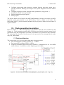
BE électronique automobile
5 e année ESE
Presentation of MPC5604B
MCU (Qorivva)
http://www.alexandre-boyer.fr
Alexandre Boyer
Patrick Tounsi
5e année ESE
October 2013
BE électronique automobile
5 e année ESE
I - Presentation of the MCU MPC5604B .............................................................................4
II MPC5604B programming main steps ..........................................................................5
III - Clock generation description .......................................................................................6
1. Clock architecture .......................................................................................................6
2. Fast external oscillator (FXOSC) ................................................................................7
3. FM PLL ......................................................................................................................7
IV - Mode entry module (MC_ME) ....................................................................................9
1. Presentation of the different modes ...........................................................................10
2. Mode entry module registers ..................................................................................... 11
a. Enabling modes..................................................................................................... 11
b. Mode configuration ............................................................................................... 12
c. Peripheral configuration ........................................................................................ 12
d. System mode selection and transition .................................................................... 14
3. Summary – MCU initialization procedure ................................................................. 14
VWake up Unit (WKPU) ............................................................................................. 15
VI - GPIO pad configuration (System Integration Unit Lite)............................................. 16
1. Presentation .............................................................................................................. 16
2. Pad configuration ......................................................................................................16
3. GPIO Data registers .................................................................................................. 17
4. EIRQ pins ................................................................................................................. 17
VII - Interrupt configuration .............................................................................................. 18
1. Interrupt service request (ISR) in MCU ..................................................................... 18
2. Presentation of INTC and interrupt vector ................................................................. 18
3. Enabling maskable interrupt ...................................................................................... 20
4. Configuring hardware triggered interrupt .................................................................. 20
5. Configuring software triggered interrupt ................................................................... 21
VIII Analog-to-digital converter (ADC) ........................................................................ 21
1. Presentation .............................................................................................................. 21
2. ADC registers ...........................................................................................................24
a. Configuration of the pad........................................................................................ 24
b. Configuration settings of the ADC block ............................................................... 24
c. Conversion timing registers ................................................................................... 24
d. Configuration of interrupts .................................................................................... 25
e. Selection of analog inputs ..................................................................................... 25
f. Power down configuration .................................................................................... 26
g. Data registers ........................................................................................................ 26
IX - E-MIOS blocks and PWM module ............................................................................ 26
1. eMIOS blocks presentation ....................................................................................... 27
2. PWM configuration .................................................................................................. 29
XCross Triggering Unit (CTU) .................................................................................... 30
XI - Periodic interrupt Timer (PIT)................................................................................... 31
XII - Software Watchdog Timer (SWT) ............................................................................. 33
XIII CAN bus and FlexCAN module ............................................................................ 33
2
BE électronique automobile
5 e année ESE
1.
2.
3.
Hardware architecture of CAN bus ...........................................................................34
Format of data frames ............................................................................................... 35
Bit time and data synchronization ............................................................................. 37
a. Construction of the bit time ................................................................................... 37
b. Synchronization segment ...................................................................................... 37
c. Propagation segment ............................................................................................. 37
d. Resynchronization – Phase errors and resynchronization jumps ............................ 38
e. Phase segments 1 et 2 ............................................................................................ 39
4. FlexCAN module ......................................................................................................40
a. General presentation of the module and message buffers ....................................... 40
b. Principle of the configuration of the FlexCAN module ..........................................41
c. Configuration of I/O pads...................................................................................... 42
d. Configuration of the control registers .................................................................... 42
e. Configuration of bit time ....................................................................................... 43
f. Interrupt configuration .......................................................................................... 43
g. Configuration of error management ....................................................................... 44
h. Configuration of operation modes ......................................................................... 45
i.
Transmission process ............................................................................................ 45
j.
Reception process ................................................................................................. 46
k. Reception acceptance mask ................................................................................... 47
5. Implementation of the CAN bus on the starter kit TRK-MPC5604B ......................... 47
XIV SPI bus and DSPI module ..................................................................................... 49
1. Some elements about SPI protocol ............................................................................ 49
2. Presentation of DSPI module .................................................................................... 50
a. General description ............................................................................................... 50
b. TX Buffering and transmitting mechanisms .......................................................... 51
c. RX buffering and receiving mechanisms ............................................................... 52
d. Transfer attributes ................................................................................................. 52
e. Interrupts............................................................................................................... 53
3. Configuration of the DSPI module ............................................................................ 54
a. Module configuration ............................................................................................ 54
b. Clock and transfer attributes .................................................................................. 54
c. TX FIFO writing ................................................................................................... 55
d. RX FIFO writing ................................................................................................... 55
e. Interrupt configuration and status ..........................................................................56
3
BE électronique automobile
5 e année ESE
This document aims at providing basic information for application development on the
microcontroller MPC5604B. The content of the document is not exhaustive and does not
detail every part of the microcontroller (MCU). Only the peripherals and functions which are
required for the lab are presented.
Some library and code source examples are also provided to get familiar with the MCU
programming. For more technical information about the component, please refer to the
datasheet Bolero512K_RM_Rev7_07_2010.pdf. Links to the datasheet will be provided in
this document.
Remark: sometimes, the register names given in the datasheet do not match with those
provided by the MCU library MPC5604B_M27V.h. Don’t hesitate to verify the right name in
the library.
You can also refer to the MPC5600 cookbook document from Freescale, AN2865 MPC5600 cookbook.pdf, which provides several software examples to start using MPC5600
MCU family.
Your applications will be developed on evaluation boards TRK-MPC5604. Please refer to the
user manual TRKMPC5604BEVBUM.pdf for more detail about the test board, and to the
schematic TRK_MPC5604B_Rev_B_Schematic_Layout.pdf.
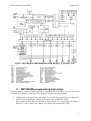
I-
Presentation of the MCU MPC5604B
MPC5604B is a MCU developed by Freescale Semiconductor and
belongs to the family MPC560x, also called Qorivva. It is a 32 bit
MCU dedicated to automotive body applications designed in
CMOS 90nm technology. Its core is based on a Power
Architecture ® and a e200z0 CPU. The version used in the Lab is
MPC5604BxLQ, which is mounted in a LQFP 144 package.
Its main characteristics are:
Up to 512 KB of Flash memory for code, and 64 KB of Flash memory for data
Up to 32 KB of SRAM memory
Core frequency up to 64 MHz, based on a frequency modulated PLL (FM PLL)
An interrupt controller (INTC) with 148 selectable priority interrupt vectors, including
16 external interrupt sources
36 channels for 10-bit analog-to-digital converters (ADC)
Up to 3 serial peripheral interface (DSPI) modules, 4 serial communication interface
(LINFlex), 6 CAN modules (FlexCAN)
Up to 123 configurable general purpose input-output (I/O)
Up to 6 periodic interrupt timers (PIT) with 32-bit counter resolution
Device testing based on JTAG bus (IEEE 1149.1)
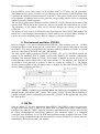
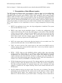
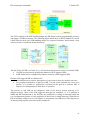
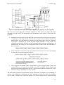
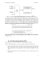
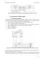
Fig. 1 presents the block diagram of the MCU.
4
BE électronique automobile
5 e année ESE
Figure 1 - Block diagram of MPC5604B (Bolero512K_RM_Rev7_07_2010.pdf - p. 32)
II - MPC5604B programming main steps
This part aims at giving the main steps for the programming of the MCU. You are not forced
to follow this sequence, it intends only to help you to start with programming.
Initialization of system clock and modes for system and peripherals (see Chapters 3
and 4 for clock generation, Chapter 5 for mode entry module MC_ME).
The operation mode must be defined at initialization for every peripheral. Enter in
RUNx (x = 0 to 3) mode (see Chapter 5 for mode entry module MC_ME)
5
BE électronique automobile
5 e année ESE
Configure input-output pads (direction, alternate function activation, output drive,
pull-up, pull-down, filtering) (see chapter 8 for System Integration Unit Lite module
SIUL)
Configure peripherals (clock, interrupt enable, parameters, energy mode…)
Installation of INTC interrupt handlers
Enable maskable interrupt requests
Main program
The register names can be found in the MPC5604B datasheet, but the given names can differ
from the actual name defined in the MCU library. Refer to Refer to the header file
MPC5604B_0M27V_0100.h (normally included in your projects) to find the correct names of
registers and bits.
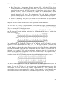
III - Clock generation description
Refer to Chapter 3 – Clock description for more details about the clock architecture and
Chapter 4 – Clock generation module (MC_CGM) for more details about the internal clock
generation. Only the configuration of FXOSC and FMPLL are presented in this document.
The activation and selection of clock sources for the system clock are managed by the mode
entry MC_ME module.
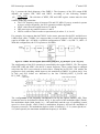
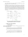
1. Clock architecture
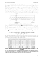
The system clock (sys_clk) can be built from three selectable sources:
Fast external quartz oscillator (FXOSC), 4 – 16 MHz
Fast internal RC oscillator (FIRC), 16 MHz
Frequency modulated phase locked loop (FMPLL), synchronized for a 4 to 16 MHz
clock reference. It can deliver a clock frequency up to 64 MHz
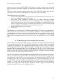
Figure 2 – Clock architecture (Bolero512K_RM_Rev7_07_2010.pdf - p. 70 – Fig. 3-1)
6
BE électronique automobile
5 e année ESE
Except FMPLL, every clock source can be divided from 1 to 32 before sys_clk generation.
Two additional low power oscillators are provided but are not detailed in this document. Fig.
2 presents the simplified clock architecture of the MCU. The system clock serves as reference
for peripherals. Peripheral clock can be gated for energy saving purpose (refer to peripheral
chapter to identify related registers).
The pin PA[0] proposes as alternate function CLKOUT, for the external observation of the
system clock. The bit EN in the register OC_EN is set to enable the output clock (see p 104).
The frequency of the output clock can be divided through the content of the register
OCDS_SC.
The quality of clock sources is checked by the Clock Monitor Unit (CMU). This module can
detect loss of clock integrity and switch to a SAFE mode in case of clock failure interrupt. It
can also be used as frequency meter. Refer to Chapter 3.8 for more information.
2. Fast external oscillator (FXOSC)
Refer to Chapter 3.3 for more information about FXOSC. This oscillator uses a 4 – 16 MHz
external oscillator circuit. It can provide a clock source for the system clock and an input for
the FMPLL. The energy management, the activation and the selection of FXOSC as system
clock are controlled by the mode entry MC_ME module.
The only register which controls the FXOSC is FXOSC_CTL (p 73). OSCBYP controls the
bypass of the oscillator, EOCV counter specifies the duration for oscillator stabilization
checking. The interrupt linked to FXOSC clock failure is enabled by the bit M_OSC. The
related interrupt request (IRQ) vector is the vector number 57. The flag bit I_OSC indicates if
an oscillator clock interrupt is pending. It must be cleared by writing a ‘1’. The output
division factor applied on the oscillator clock is defined by the field OSCDIV[4:0]. The
division factor is equal to OSCDIV+1.
After reset, FXOSC is placed in powerdown mode. Its switch on is controlled by software
through the MC_ME module (ME_<mode>_MC register, FXOSCON bit). The availability of
a stable oscillator clock is indicated by the status bit S_FXOSC in the register ME_GS of the
MC_ME module.
3. FM PLL
Refer to chapter 3.7 for more information about FMPLL. The FMPLL enables the generation
of high speed clock (from 16 MHz to 64 MHz) from 4-16 MHz clock source, which can be
configured by software. FMPLL supports frequency modulation of the system clock in order
to reduce electromagnetic interference emission. The modulant signal is a triangular
waveform, with frequency up to 100 KHz and modulation depth comprised between 0 and
2 %. The energy management, the activation and the selection of FMPLL as system clock are
controlled by the mode entry MC_ME module.
7
BE électronique automobile
5 e année ESE
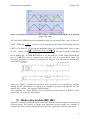
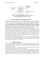
Fig. 3 presents the block diagram of the FMPLL. The frequency of the PLL output (PHI)
depends on register IDF, ODF and NDIV, according to the following formula:
clkin NDIV
. The selection of NDIV, IDF and ODF register content must be done
phi
IDF ODF
with the following constraints:
The VCO frequency range is between 256 and 512 MHz. If you try to make it operate
at lower or larger frequency, the PLL operation could be degraded.
NDIV values must be ranged between 32 and 96
IDF can accept any number between 1 and 15
ODF is coded on 2 bits in order to represent only 4 values: 2, 4, 8 or 16
For example, let’s suppose that the FXOSC is the source generator for the PLL and delivers a
8 MHz clock: clkin = 8 MHz. Let’s suppose that we want to generate a PLL output frequency
equal to 45 MHz: phi = 45 MHz. A possible configuration is: NDIV = 90, IDF = 2, ODF = 8.
With this configuration, the VCO operates at 360 MHz.
Figure 3 – FMPLL block diagram (Bolero512K_RM_Rev7_07_2010.pdf - p. 80 – Fig. 3-6)
The configuration of the PLL operation is controlled by the register FMPLL_CR. The register
fields IDF, ODF and NDIV sets the PLL output frequency. These values must be changed
only when the PLL is not selected as clock source. Setting the bit EN_PLL_SW enables the
progressive clock switching which improves the transition to FMPLL as system clock. Loss
of lock and PLL failure are indicated by the bits UNLOK_ONCE, S_LOCK and
PLL_FAIL_FLAG.
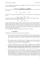
The configuration of the frequency modulation is set by the register FMPLL_MR. Three
parameters need to be defined as shown in Fig. 4: the period of the modulant signal (Tmod),
the modulation depth (Mod_depth (%) = 100×md/Fmod) and the type of spreading (center
spread or down spread), where Fmod is modulation frequency and md the amplitude of
frequency excursion. The modulation depth or index is limited to +/-2 % (center spread) ou 4 % (down spread), the maximum modulation frequency is 100 KHz.
8
BE électronique automobile
5 e année ESE
Figure 4 – Frequency modulation principle in FMPLL block (Bolero512K_RM_Rev7_07_2010.pdf
- p. 87 – Fig. 3-10)
The field MOD_PERIOD sets the modulant period. Its equivalent binary value is equal to:
Fref
, where Fref is the frequency at the output of the feedback divider
MOD _ PERIOD
4 Fmod
(NDIV). The field INC_STEP sets the modulation index. Its equivalent binary value is equal
215 1 NDIV Mod _ depth %
to: INC _ STEP round
. The type of spread is defined by
100 5 MODPERIOD
the bit SPRD_SEL. If STRB_BYPASS bit is set, the field INC_STEP, MOD_PERIOD and
the bit SPRD_SEL must be changed only when the PLL is in powerdown mode. The
frequency modulation is enabled by setting the bit FM_EN. The FM must be enabled only
when the PLL is active.
After reset, FMPLL is placed in powerdown mode. Its switch on is controlled by software
through the MC_ME module. Its switch on is controlled by software through the MC_ME
module (ME_<mode>_MC register, FMPLLON bit).
The availability of a stable FMPLL clock is indicated by the status bit S_FMPLL in the
register ME_GS of the MC_ME module.
IV - Mode entry module (MC_ME)
This block controls the different modes of the MCU and the transition sequences between the
different modes. The notions of modes and transitions between modes are essential to
configure the MCU correctly and initiate the user mode, which the normal operation mode.
9
BE électronique automobile
5 e année ESE
Refer to chapter 5 – Mode entry module for more details about the MPC5604’s modes.
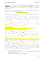
1. Presentation of the different modes
The MCU proposes different modes corresponding to different usages (system configuration
and monitoring, user mode, low power modes…) (refer to table 5-1 p 113/956). The
embedded software executes only in DRUN, SAFE, TEST and RUN0..RUN3 modes. RESET,
DRUN, SAFE and TEST modes are system modes. They are dedicated to the configuration
and the monitoring of the system. RUN0..RUN3, HALT0, STOP0 and STANDBY0 are user
modes. HALT0, STOP0 and STANDBY0 are low power modes. In the next chapter (Wakeup
Unit), the procedure to exit these low power modes will be detailed. The configuration of the
MCU mode depends on the requirements in term of energy management and processing
power.
RESET: the application is not active, the chip configuration is initialized. The system
enters in this mode after a reset.
DRUN: entry mode for the embedded software. It enables the configuration of the
system at the start-up. This is the only mode entry to a user mode. If the embedded
software does not enable a transition between DRUN mode and a user mode, the main
program defined by the user cannot execute. The system enters in this mode after the
end of Reset mode, and after software request from RUN0..RUN3, SAFE, TEST
modes, and a wake up request from STANDBY mode.
SAFE: the system enters in this mode after the detection of a recoverable error. The
system exits this mode after a reset or DRUN from software.
TEST: for device self-test. The system enters in this mode from DRUN mode by
software request. The system exits this mode after a reset or by software request to
come back in DRUN mode.
RUN0 .. RUN3: these are the embedded software modes where most processing
activity is done. 4 RUN modes are provided to enable different power and clock
configuration. The system enters in one of these modes after DRUN by software
request, interrupt event from HALT0, interrupt or wake up event from STOP0. The
system exists one of these modes after reset, entry in SAFE mode after an hardware or
software error, HALT0, STANDBY0 or STOP0 by request.
STOP0: Reduced activity low power mode. The wakeup signals are processed rapidly,
contrary to HALT mode. By default system clock is FIRC, but it can be switched off.
The data and flash memories are powered down but can be activated; the main
regulator is switched on. See chapter Wakeup Unit for more details about the exit of
STOP0 mode.
HALT0: Reduced activity low power mode. The clock core is disabled. The analog
peripherals can be switched off. The system enters in this mode by software request
from RUN0..RUN3 modes. The systems leaves this mode after a reset, after a
hardware or software failure to go in SAFE mode, or interrupt event to come back in
10
BE électronique automobile
5 e année ESE
previous RUN0..RUN3 modes. Contrary to STOP0 and STANDBY0 modes, wakeup
signals cannot be used to exit from HALT0 mode.
STANDBY0: This is the most low power mode which ensures a reduced leakage
current. Most of the blocks of the MCU are switched off from the power supply to
reduce leakage current. Wake up from this mode is quite long. The system enters in
this mode by software request from DRUN, RUN0..RUN3 modes. The system leaves
this mode after reset, of after wake up event to enter in DRUN mode (see chapter
Wakeup Unit). The wakeup from STANDBY0 mode is longer than from STOP0 mode.
All the pins are in high impedance mode. Only the reset generation mode, power
control unit, wake up unit, 8K RAM, RTC/API, CAN sampler, SIRC, FIRC, FXOSC
are powered.
Figure 5 – Mode entry diagram and possible mode transitions
(Bolero512K_RM_Rev7_07_2010.pdf - p. 144 – Fig. 5-24)
2. Mode entry module registers
a. Enabling modes
The Mode Enable Register MER allows enabling or disabling some MCU modes (except
RESET, DRUM, SAFE and RUN0).
11
BE électronique automobile
5 e année ESE
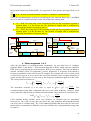
b. Mode configuration
A mode configuration register is associated to each mode to control the connection or
disconnection of some peripherals in the mode, such as the I/O output buffers, internal voltage
regulator, data and code flash memory, PLL, fast external crystal and RC oscillators. It
specifies also the system clock used by the system (PLL, crystal oscillator, fast RC
oscillator…). All these registers have the same structure. The following figure shows the
register structure for RUN0 .. RUN3 mode configuration registers, called ME.RUN[0] to
ME.RUN[3].
c. Peripheral configuration
Up to eight different behaviors can be configured for the peripherals of the MCU in the
different run modes. These 8 behaviors are defined by the Run Peripheral Configuration
Registers 0 to 7 (RUNPC[0] to RUNPC[7]).
Setting a bit associated to a mode to ‘0’ means that, if this configuration is given to a
peripheral, this peripheral will be frozen in with clock gated during this mode. If this bit is set
to ‘1’, the peripheral will be active. For example, let’s suppose that we define one behavior in
RUNPC[0] and we write 0x00000030. If this configuration is associated to one peripheral,
this peripheral will be active only in RUN0 and RUN1 mode. In all other modes, it will be
frozen.
For the 3 non run modes (STANDBY0, HALT0 and STOP0), 8 behaviors can also be
configures through the registers Low Power Peripheral Configuration LPPC[0]to LPPC[7].
12
BE électronique automobile
5 e année ESE
Once the different possible behaviors have been configured with registers RUNPC[0]to
RUNPC[7], these behaviors can be associated to the 144 peripherals of the MCU. 144
registers called Peripheral Control Registers PCTL[0]to PCTL[143] are associated to each
peripheral. These registers contains 3 fields: the field RUN_CFG defines which one of the 8
behaviors defined in RUNPC[0] to RUNPC[7] will be associated to the peripheral during the
run modes. The field LP_PC defines which one of the 8 behaviors defined in LPPC[0] to
LPPC[7] will be associated to the peripheral during the non run modes. The bit DBG_F sets
the behavior of the peripheral in Debug mode.
The status of the peripherals is given by the registers PS0, PS1, PS2 and PS3.
Remark: one number from 0 to 143 is associated to each peripheral. The following table
(Table 3-1 p 71/956) gives the number associated to each peripheral. For example, the number
32 is associated to the ADC block, the number 68 to the SIUL module (GPIO). The
configuration of the ADC behavior according to the mode will be defined by register
PCTL[32] and the configuration of the SIUL behavior by PCTL[68].
13
BE électronique automobile
5 e année ESE
d. System mode selection and transition
The Mode Control Register MCTL is used to trigger mode change by software. The
TARGET_MODE field defines the target mode to be entered by software request.
The KEY field is a control key to enable the writing in this register. The KEY is 0x5AF0. A
different value is invalid and any writing in the register will be ignored. Actually, two writing
of the register have to be done to force the device to enter in the mode defined by
TARGET_MODE: first time with the good value of the key, a second time with the inverted
value of the key. For example, suppose that we want the system to exit DRUN mode to enter
RUN0 mode. The TARGET_MODE field must be equal to ‘0100’. Therefore, the two
following lines have to be written in the software:
ME.MCTL.R = 0x40005AF0;
/* Enter the target mode and the Key */
ME.MCTL.R = 0x4000A50F;
/* Enter the target mode and the inverted Key */
The global mode status of the system is given by the register Glogal Status Register GS. The
field S_CURRENTMODE notifies the current device mode. The bit S_MTRANS notifies if a
mode transition is on-going. It gives also the status of several MCU peripherals.
3. Summary – MCU initialization procedure
The procedure to initialize the MCU is always the same and describes below. This procedure
must be done in DRUN mode.
1. Enables the modes to be used
2. Configure the clock sources
3. Configure the modes to be used
4. Configure the peripherals
14
BE électronique automobile
5 e année ESE
5. Switch from DRUN mode to a user mode (RUN0,1,2,3)
Remark:
When the MCU is in debug mode, the Software Watchdog (SWT) is disabled (See chapter
Software Watchdog). In nominal operation, the SWT is activated. The SWT must be stopped
or checked regularly to avoid unwanted MCU reset. Refer to chapter Software Watchdog of
this document or chapter 28.2 of the MCU datasheet from more information about the
configuration of the SWT.
V - Wake up Unit (WKPU)
This block manages the events which trigger a transition from low power modes (HALT0,
STOP0 and STANDBY0) to RUN0..3 or DRUN modes. Refer to chapter 30 – Wakeup Unit
for more details.
The microcontroller exits a low power mode either after a reset assertion, a interrupt request
or a wakeup event (except for Halt0 mode). The wakeup signal can originate from 20 sources,
either internal (API and RTC) or external (specific pads such as CAN or LIN), as shown in
the following table. Three interrupts are associated to these events.
15
BE électronique automobile
5 e année ESE
Several registers are dedicated to the configuration and the management of wakeup events.
The register WIFER enabled the different wakeup sources. Writing a ‘1’ in one of the 20
positions of the field IFE[19:0] enables one the wakeup event (see previous table to find the
number associated to a wakeup source).
The register IRER enables interrupts generation when wakeup events are detected. The
register WISR contains the interrupt flags. The wakeup event is activated either on rising or
falling edge, depending on the configuration of register WIREER and WIFEER.
VI - GPIO pad configuration (System Integration Unit
Lite)
Refer to Chapter 8 – System Integration Unit Lite for the configuration of General Purpose
I/O (GPIO) pads and the multiplexing of alternate functions associated to GPIO.
1. Presentation
MPC5604B proposes 123 GPIO in its LQFP144 package version, organized in 8 ports (from
Port A to H). Except port H, each port contains 16 I/O pads. All the pad can be configured
independently through the PCR[0] to PCR[122] registers. The number of the PCR register
related to a given pad can be found in Table 2-3 p. 45. For example, the pad PA[0] is
associated to the register PCR[0], pad PA[1] to PCR[1] and pad PH[10] to PCR[122].
One input register GPDI and one output register GPDO are associated to each pad. 15 GPIO
are associated to External Interrupt Request (EIRQ) pins (EIRQ[0:15]). They can trigger
interrupt on rising edge or falling edge events, depending on the configuration of registers
SIUL_IREER and SIUL_IFEER. Some glitch filter can be configured at the input of these
pins.
2. Pad configuration
The 123 pads of SIUL can be individually configured by the registers PCR[0] to PCR[122].
Four output buffer, the alternate function is selected by the field PA[1:0]. Up to 4 alternate
functions are associated to a pad. By default, the field is equal to ‘00’ and the pad operates as
a GPIO. In case of GPIO mode, the output buffer is enabled if OBE bit is set. The output
driver can be configured as open drain output through the bit ODE. The SRC bit controls the
16
BE électronique automobile
5 e année ESE
slew rate of the output pad. By default, the pad is slow. By setting SRC to ‘1’, the pad is
configured as medium or fast.
For input pad, the input buffer is enabled by the bit IBE. If the pad is used as analog input, the
bit APC must be set. WPE and WPS bits enable weak pull-up and pull-down device on a pad.
In some cases, the input signal of a peripheral (such as CAN, LIN, SPI buses) can be provided
by several pins. For example, the reception input of CAN1 module CAN1_RXD can be
provided by three pads: PC[3], PC[11] or PF[15]. It is therefore necessary to specify the
associated pad. First, the correct alternate function has to be selected on the PCR register of
the pad. Then, the pad used for the peripheral is specified in the register PSMI. See Table 813 p. 218 for the configuration of PSMI registers.
3. GPIO Data registers
Data can be read or write pad by pad or port by port. The data are written on individual output
pads by the bit PDO of the registers GPDO[n], n = 0 to 123. The data are read from individual
input pads by the bit PDI of the registers GPI[n], n = 0 to 123.
A port can be completely written or read in one operation by the registers PGPDO0 –
PGPDO3 (output data) and PGPDI0 – PGPDI3 (input data). The most significant bit of the
parallel port register corresponds to the least significant pin in the port. For example, bit PA[0]
is mapped to the most significant bit of PGPDO0 and bit PB[15] is mapped to the least
significant bit of PGPDO0.
It is also possible to write on output ports through a mask, defined by the registers MPGPDO0
to MPGPDO7. Each 32 bit register is associated to one port. The 16 most significant bits of
the register define the mask (field MASK). The 16 least significant bits define the data to be
written on the output buffer (field MPPDO).
4. EIRQ pins
16 GPIO are also defined as external IRQ input pins. Any rising or falling edge events can
trigger maskable interrupts. Two interrupts are associated to EIRQ. The 8 first EIRQ are
associated to interrupt request IRQ0 (interrupt vector number 41), the 8 last EIRQ are
associated to interrupt request IRQ1 (interrupt vector number 42).
The interrupt request associated to each EIRQ input can be individually enabled by the
register IRER. Each time an interrupt is pending, the flag bit EIF of the register ISR is set to
17
BE électronique automobile
5 e année ESE
‘1’. Writing a ‘1’ clears the flag. Interrupt can arise on rising and/or falling edge events on
EIRQ input pins. It can be configured by the registers IREER and IFEER.
Noise coupled on input pins can induce glitches that may be misread as a rising or falling
edge. Therefore, digital glitch filter can be enabled on each EIRQ inputs, by setting bits IFE in
IFER register. The digital glitch filters are configured by the registers IFMC0-IFMC15 and
IFCPR0-IFCPR15.
VII -
Interrupt configuration
Refer to Chapter 10 – Interrupt Controller (INTC) for the configuration of priority of the
different interrupt source.
1. Interrupt service request (ISR) in MCU
All the real-time controllers in interaction with their environment operate by interruption of
their on-going program. The execution of functions depends on external events (e.g. pushed
button, detection of a voltage above a given threshold, reception of a signal…). The interrupt
service requests (ISR) are predefined and associated either to hardware peripherals, resets or
software requests. When the conditions for the triggering of an interrupt are detected by the
CPU, the execution of a function dedicated to the ISR processing can launched, depending on
the interrupt configuration (interrupt enabled or not if the interrupt is maskable), the content
of interrupt vector table and the level of priority of the ISR.
The interrupt vector table is an area of the memory divided in interrupt vectors. Each interrupt
vector has a fixed memory address and is associated to a given ISR (e.g. edge detection on an
input digital buffer or time-out of a timer). At the address of the interrupt vector, the memory
contains the address of the function dedicated to the processing of the ISR (for example, when
an edge is detected on an input digital buffer, the programmer wants to launch a program that
switch on an external LED). The programmer must know exactly the address of interrupt
vector in order to associate an ISR to the execution of a processing function.
When an ISR is triggered during the execution of the main program, the address of the next
instruction of the main program must be saved, in order to come back to the main program
after the processing of the interrupt. In practice, before stopping the execution of the main
program and launch the interrupt program, the content of the program counter is saved and
will be updated at the end of the interrupt program.
The interrupt management is complex and is done by an interrupt controller (INTC) which
aims at scheduling the ISR, i.e:
Notifying the CPU that an ISR is transmitted by a peripheral or the software
Managing the priorities between the different incoming ISR
Transmitting to the CPU the address of the program to process the interrupt
2. Presentation of INTC and interrupt vector
The following figure describes how interrupt requests are handling and the position of the
INTC block. In the MCU core (e200z0h), registers called Interrupt Vector Offset Register
(IVOR) forms a branching table which handles the different exceptions which occur during
the MCU operation. IVOR4 is the register used for interrupt handling.
18
BE électronique automobile
5 e année ESE
The INTC module of the MPC5604B manages the ISR based on their programmable priorities
and triggers IVOR4 exceptions. The following figure details how an ISR is handled in a mode
called software mode (two ISR handling modes are proposed: hardware and software. Only
software mode is considered in this document).
The MCU has 142 ISR (see Table 10-1 p 242 for the detail about the source of available ISR):
134 ISR are associated to peripherals (hardware (HW) triggered ISR)
8 ISR which can be configured by software (software (SW) triggered ISR)
Remark: SW triggered ISR are dedicated to:
In a multiprocessor context, interruption of a processor activity by another processor
In a program launched by a high level ISR, if a part of the program has a low level
priority, it is possible to suspend the execution of this part by a software ISR. It
improves the management of dead-lines of operation.
The priority of each ISR can be configured, with a level from 0 (lowest priority) to 15
(highest priority). Most of the HW triggered interrupts are maskable, i.e. it is possible to
inhibit the ISR transmission to the INTS by the peripheral, by setting an interrupt enable bit
(see configuration registers of each peripheral to know how to mask interrupt). Each time an
ISR is launched, a flag bit is set. One flag bit is associated to one ISR source. The flag bits are
in interrupt flag registers associated to the peripherals.
19
5 e année ESE
BE électronique automobile
Important: don’t forget to reset flag bit after ISR triggering. The flag indicates to the INTC
that the peripheral sent an ISR. If the flag remains set, no more ISR can be generated. Most of
the time, it is necessary to write a ‘1’ in the flag bit to reset it. This is a particularity of
Freescale MCU.
Table 10-10 p. 253 gives the interrupt vector table of the MPC 5604B. The address of an
interrupt vector is given in the following format:
Base address + Vector number
The vector number starts at 0 (for the software ISR number 0) up to 210 (for ISR launched by
buffers 32 to 63 of FlexCAN5).
In order to associate an ISR coming from a peripheral or the software and a program to
process the ISR, an interrupt handler has to be defined. This interrupt handler writes the
address of the interrupt processing program at the interrupt vector address, and manages the
ISR priority. We will see how to deal with interrupt handler with hardware or software ISR in
the MPC5604B.
3. Enabling maskable interrupt
Maskable interrupt must be enabled at two levels: at local level (i.e. at peripheral level) by a
interrupt enable bit associated to ISR source, and at global level. In order to enable ISR in the
MCU, you must execute this routine in your program:
void enableIrq(void) {
INTC.CPR.B.PRI = 0;
asm(" wrteei 1");
}
/* Single Core: Lower INTC's current priority */
/* Enable external interrupts */
4. Configuring hardware triggered interrupt
HW triggered interrupt are most of the time maskable interrupt, so the peripheral
configuration must enable ISR and the maskable interrupt must enabled at global level. INTC
is implemented in several files: INTCInterrupt.h, INTCInterrupt.c, Eceptions.h, Exceptions.c.
They contain the routines used to execute the ISR handling procedure. The following function
configure the interrupt handler and the interrupt priority:
INTC_InstallINTCInterruptHandler(My_ISR_program,vector_number,priority_level);
My_ISR_program is the name of the program that the programmer wants to launch when the
ISR is triggered by the peripheral. Vector_number is the number of the interrupt vector
associated to the ISR (see Table 10-10 p. 253). Priority_level is the level of priority associated
to the ISR and ranges from 0 to 15.
For example, let’s suppose that you design a program that launches the periodic interrupt
timer Timer PIT1. At each time-out of PIT1, you want to trigger an interrupt that launches a
function called My_PIT_ISR_function. The vector number of the ISR associated to PIT1 is 60
(according to Table 10-10 p. 253). You want to give a priority level equal to 2 to the PIT1 ISR.
In order to enable the PIT interrupt, you have to proceed as following:
1. Initialize PIT1 and enable interrupt
2. Interrupt handler for the PIT1 ISR:
INTC_InstallINTCInterruptHandler
(My_PIT_ISR_function,60,2);
3. Enable maskable interrupt in the MCU: enableIrq();
20
BE électronique automobile
5 e année ESE
4. In the function My_PIT_ISR_function, you have to clear the flag associated to PIT1
ISR.
5. Configuring software triggered interrupt
Use the same procedure as HW triggered interrupt to configure SW triggered interrupt.
The only difference relies in the triggering of software interrupt. Hardware interrupt is
triggered by a hardware event (external event, time-out of a timer…). A software interrupt is
triggered by a program request.
The registers SSCIR[i], i = 0..7, of the INTC modules support the setting or the clearing of
software configurable ISR. A couple of 2 bits : SETi/CLRi sets or clear each software ISR.
Writing a ‘1’ to SET set the flag bit CLR to ‘1’.Writing a ‘0’ has no effect. If the CLR bit is
set to ‘1’ it indicates that an ISR is pending, like any other flag bit. The flag CLR is cleared by
writing a ‘1’.
VIII -
Analog-to-digital converter (ADC)
Refer to Chapter 26 – Analog-to-Digital Converter (ADC) for the principles and the
configuration of ADC.
1. Presentation
The ADC block contains 36 analog channels internally multiplexed to the 10 bit resolution
ADC machine. These 36 analog channels are divided between:
16 precision channels called ANP[0]to ANP[15]
20 standard channels called ANS[0] to ANS[15] and ANX[0] to ANX[3] which are
externally multiplexed.
21
BE électronique automobile
5 e année ESE
Figure 6 – Block diagram of ADC (Bolero512K_RM_Rev7_07_2010.pdf - p. 726 – Fig. 26-1)
The conversion can be triggered by software or hardware (CTU block (see chapter IX of this
document) or timer PIT2, not described in this document). Three types of conversion are
proposed:
Normal conversion mode: in this mode, the conversion process consists in two phases:
a sampling of an analog channel, and then the conversion of the sampled channel. In
normal mode, two sub-modes are proposed: in one shot mode, only one sequential
conversion is launched for all the activated analog channels. In scan mode, the
sequential conversions are done on each activated analog channels continuously. In
normal mode, the change of the configuration must be done before the launching of
the conversion.
Injected channel conversion mode: the normal conversion process can be interrupted
to inject the conversion of another channel.
CTU triggered conversion mode: improvement of the injection mode, where the
synchronization is provided by an external event (PIT3 or eMIOS block). Normal and
injected conversions triggered by the CPU are still enabled. Refer to chapter IX of this
document for the configuration of CTU module.
The ADC block proposes several features for the conversion. It proposes a pre-sampling. It
consists in precharging or discharging the ADC sampling capacitor just before the sampling
step, in order to improve the conversion quality. Two fixed voltages can be sampled during
22
5 e année ESE
BE électronique automobile
this operation: Vdd_HV_ADC or Vss_HV_ADC, which are two external voltage references
for the ADC.
The conversion timing can be configured accurately, with the register CTR. The ADC is
clocked by the peripheral clock, or by the peripheral clock with a frequency divided by 2. The
CTR register defines for each type of channel the three step of a conversion: the sampling
phase (the ADC sampling capacitor is connected to the selected analog channel), the latching
phase (the sampling capacitor is disconnected of the analog channel, this sequence lasts one
half a ADC clock period), and the evaluation phase (this is the analog-to-digital conversion,
based on a successive approximation, which can last 10 clock period for a 10 bit conversion).
Figure 7 – Sampling and conversion timings (Bolero512K_RM_Rev7_07_2010.pdf - p. 731 – Fig.
26-4)
The CTR register is composed of three fields to configure the conversion time: INPLATCH,
INPCMP and INPSAMP. The conversion time can be computed according to the following
formula:
TSample INDSAMP N delay .TClk , INDSAMP 3 , N delay 0.5 si INDSAMP 0 x06 , sin on 1
TEval
10 .TEval
10 .INPCMP .TClk , INPCMP 1, INPLATCH
TConv
TSamp
TEval
INPCMP
N Delay .Tclk
The INPCMP and INPSAMP configurations are limited if the clock frequency is greater than
20 MHz. The selection of correct values for these fields can be delicate. The following table
gives nominal values depending on ADC clock frequency.
Figure 8 – ADC sampling and conversion timings (Bolero512K_RM_Rev7_07_2010.pdf - p. 731
– Table 26-1)
The ADC block proposes also a programmable analog watchdog. This function verifies if a
conversion result belongs to a predefined voltage interval, set by the threshold registers
THRH and THRL which define the upper and lower limits of the interval.
23
BE électronique automobile
5 e année ESE
Several maskable interrupt are proposed. Several end-of-conversion interrupts are proposed:
EOC (end of a conversion), ECH (end of conversion of a chain), JEOC (end of an injected
conversion), JECH (end of injection chain), EOCTU (end of conversion in CTU conversion
mode). Interrupts are also associated to the analog watchdog: WDGxL and WDGxH which
indicates which thresholds have been crossed.
The ADC proposes two low-consumption modes: the power down and auto clock-off modes.
The power-down mode is the nominal mode after reset. All the configurations of the ADC
must be done in power-down mode. The conversion cannot start in power-down mode. If a
power-down mode entry is requested while a conversion is on-going, the conversion must be
completed before entering in low-power mode.
In auto clock-off mode, the ADC clock is switched off and no conversion can be performed.
2. ADC registers
a. Configuration of the pad
It is important to enable the I/O pad associated to an analog channel as an analog input. The
APC bit of the PCR register associated to the pad must be set to ‘1’ (refer to part V – GPIO
pad configuration).
b. Configuration settings of the ADC block
All the configurations of the ADC (conversion mode, power-down mode, start of
conversion…) are provided by the Main Configuration Register (MCR). The configuration of
the ADC must be done in low-power mode. The bit MODE selects if a scan mode or a oneshot mode is configured in normal mode. The bit NSTART starts a normal conversion.
Writing a ‘1’ launches the conversion. The bit is set to ‘0’ at the end of the conversion.
Writing a ‘0’ stops the current chain conversion. ADCLKSEL set the ADC clock frequency to
the 1x or 1/2x the peripheral clock frequency. Writing a ’0’ to the PWDN bit forces the ADC
to quit the power down mode to the IDLE mode. It is necessary to start conversions. Writing a
‘1’ is a request to enter in power down mode.
The register Main Status Register (MSR) provides status of the ADC (normal conversion ongoing, current conversion channel address, power-down mode…).
c. Conversion timing registers
Three Conversion Timing Registers are proposed: CTR[0] for internal precision channels
(ANP[0] to ANP[15]), CTR[1] for internal standard channels (ANS[0]to ANS[15] and
ANX[0] to ANX[3]), and CTR[2] for external multiplexed channels. See part 1 for the
configuration of INPLATCH, INPCMP and INPSAMP fields.
24
BE électronique automobile
5 e année ESE
d. Configuration of interrupts
Several registers are proposed to mask the maskable interrupts associated to the ADC block.
The Interrupt Mask Register (IMR) enables End-of-Conversion type interrupts. The interrupts
are enabled by writing ‘1’ in register bits.
The register Interrupt Status Register (ISR) gives the interrupt flags associated to the
maskable interrupt enabled by IMR register.
Interrupts can be associated to the end of conversion of each channel with the Channel
Interrupt Mask Registers CIMR[0..2]. Precision channels are associated to register CIMR[0],
standard channel to CIMR[1].
The register Channel Pending Register CEOCFR[0..2] gives the interrupt flags associated to
the maskable interrupt enabled by CIMR register.
End of conversion interrupts are associated to interrupt vector number 62 (report to Table 1010 p 253/956).
e. Selection of analog inputs
The selection of enabled analog inputs in a normal conversion chain is done with Normal
Conversion Mask Register NCMR[0..2]: NCMR[0] for precision channels (ANP[0] to
ANP[15]), NCMR[1] for standard channels (ANS[0] to ANS[15] and ANX[0] to ANX[3]).
The configuration of this register must be done in low power mode. Writing a ‘1’ in the bit
corresponding to an analog channel selects this channel in the conversion chain. For example,
if a normal mode is selected in Scan mode, if CH1 = ‘1’ and CH7=’1’ only (all the other bit
set to ‘0’), the following conversion sequence will be done continuously: sample/convert
channel 1, sample/convert channel 7, sample/convert channel 1, sample/convert channel 7….
25
BE électronique automobile
5 e année ESE
The selection of injected channels is done with the JCMR[0..2] registers.
f. Power down configuration
As explained previously, the request of power down entry or exit is set with PWDN bit in
MCR register. It is possible to configure the delay between the exit of power down mode and
the start of the conversion with the Power Down Exit Delay Register (PDEDR).
g. Data registers
ADC conversion results are stored in data registers. There is one data register per analog
channel. There are 96 Channel Data Register CDR[0..95]. CDR[0]to CDR[15]are associated
to analog precision channels, CDR[32..47] to the standard channels. A CDR register is
organized as follows: several bit to give a status of the conversion result, and the 10 bit
conversion result (filed CDATA). The alignment of the data (right or left alignment) is set by
the register WLSIDE in MCR register.
The bit VALID notifies if CDATA comes from a valid conversion. This bit is automatically
cleared when the data is read. The bit OVERW notifies that the previous converted data has
been overwritten by a new conversion. The field RESULT[0:1] reflects the conversion mode
for the corresponding channel.
IX - E-MIOS blocks and PWM module
The eMIOS blocks (Configurable Enhanced Modular IO Subsystem) is dedicated to the
measurement and the generation of timing events (e.g. capture/compare functions, generation
of pulse width modulation (PWM) signals). In this part, only a basic presentation of the
structure of the bloc will be provided and the configuration for PWM generation will be given.
26
BE électronique automobile
5 e année ESE
Refer to Chapter 25 – Configurable Enhanced Modular IO Subsystem for more details about
this block and the configuration of all the other functions.
1. eMIOS blocks presentation
The eMIOS block proposes several Unified Channels which can perform a list of timing
measurement and generation functions, according to the software configuration. The hardware
and the operation principles are detailed in Chapter 25 of the reference manual of MPC5604B,
but most of them are out of the scope of this document.
The MCU contains two eMIOS blocks: E_MIOS_0 and E_MIOS_1. Each e-MIOS block is
made of 28 unified channels, as shown in Fig. 9. Each unified channel is associated to an
input/output (I/O) pad, as alternate function (called E0UC or E1UC in Table 2-3). Even if
each channel is based on the same hardware architecture, 5 types of channel exist that differ
from the offered function.
The clock of e-MIOs blocks is provided by the system clock that can be divided by a
programmable prescaler. The operation of channels can be synchronized by internal counters
(only for types G and X channels), or by counter buses driven by other channels. The counter
and counter buses are 16 bit long. In this last mode, several channels can be synchronized.
Five counter buses are shared by channels: A, B, C, D and E. Only type X channels can drive
the counter buses. The counter bus A is the default counter bus used by every channels, it is
driven by channel 23.
27
BE électronique automobile
5 e année ESE
Figure 9 – eMIOS block organization (Bolero512K_RM_Rev7_07_2010.pdf - p. 676 – Fig. 25-1)
The unified channels propose up to 12 functions, that we will not detail. The functions are
based on the same hardware, which is activated or not according to the user-defined software
configuration. The default function is GPIO. This mode is required when the configuration of
e-MIOS channel has to be changed.
The basic operation of the channel relies on a counter that increments or decrements an
internal value, and two readable or writable internal registers (called A and B). Their
respective roles depend on the selected mode. When some predefined events arise, the counter
can be stopped, its content can be written in register, flags can be raised and/or an flip-flop
connected to the output pad can be toggled. For example, in input capture mode, when a rising
or falling edge arise on an input signal, the value of the internal counter is written in register
A and the counter internal value is reset to 0.
Second example: in PWM mode, two values are written in registers A and B. They define the
waveform of the PWM signal (period, duty cycle, leading and trailing edges position). Each
time the counter value matches with register A or B content, a flag can be raised and the
output flip-flop state is changed.
Unified channels propose 4 PWM generation modes:
28
BE électronique automobile
5 e année ESE
Buffered Output Pulse Width Modulation (OPWMB): basic PWM generation mode.
The configuration sets the placement of leading and trailing edges of the PWM signal
in a given period. Every PWM generation mode is double buffered, i.e. each time you
change the period or the duty cycle parameters, the transition is smoothed. The new
parameters are taken into account only at the end of a PWM period.
Buffered Output Pulse Width Modulation with Trigger (OPWMT): in this mode,
several PWM channels can have the same leading edge position, but different trailing
edge.
Buffered Output Pulse Width and Frequency Modulation (OPWFMB): in this mode,
both the frequency and the duty cycle can be changed.
Centered aligned Output PWM Buffered with Dead Time (OPWMCB): the leading
and trailing edge appears after and before the beginning and the end of a period.
2. PWM configuration
In this part, we will present only the basic configuration of OPWMB mode.
PWM mode requires an I/O pad, so that the PCR register of this I/O pad must be carefully
configured (refer to part V of this document). The alternate function has to be selected by the
PA bit field. It is not necessary to activate the output or the input buffer of the I/O, since the
pad is connected to the output flip-flop of the unified channel.
First, the e-MIOS block has to be configured, by the Module Configuration Register MCR (p.
678). Setting the bit MDIS ensures the entry in low power mode of the e-MIOS block. The
GPRE[0:7] field configures the e-MIOS block clock frequency by setting the prescaler value.
The e-MIOS clock frequency is equal to the system clock frequency divided by GPRE+1. The
e-MIOS clock prescaler and internal clock are enabled if bit GPREN is set. The bit GPBE
enables the global time base and the internal counter operation. Setting the bit FRZ ensures
that the internal counters of unified channels will be stopped when the MCU enters in debug
mode.
Then, the configuration of each used unified channel has to be done, with the registers UC
Control Register (CCR), UC A and B registers (CARD and CBDR, which are 16 bit registers).
The bit field MODE[0:6] configures the function of the channel. The BSL[0:1] selects the
counter source (internal or counter buses A, B, C, D or E). The bit EDPOL determines the
polarity of the PWM signal. UCPREN an UCPRE[0:1] enables a channel prescaler to divide
the counter frequency.
29
BE électronique automobile
5 e année ESE
Let’s detail the configuration of OPWMB mode. First, the period of the PWM channel is
defined by the time required by the counter to count from 0 to the maximum value of the
counter. The counter can be provided by another unified channel configured in Modulus
Counter Buffer mode (MCB) which drives a counter bus. The MODE[0:6] of this channel is
set to 0x50. A channel able to drive a counter bus has to be chosen. This channel is
synchronized by an internal counter, so that the BSL[0:1] field is set to 0x3.
Secondly, the PWM mode and the origin of the counter (a counter bus) of the channel have to
chosen. The MODE[0:6] of this channel is set to 0x60 and the BSL[0:1] to 0x00 if Counter
bus A is selected, or to 0x01 if another counter bus is selected. Then, the values of registers A
and B have to be configured. In OPWMB, the registers A and B of a channel set the leading
and trailing edge positions respectively in the PWM signal period. If the maximum count
value is set to 1000 and the register A value is set to 500, the leading edge will appear at midperiod. Finally, the polarity of the PWM signal is set with the bit EDPOL, i.e the leading edge
is a rising or falling edge.
X - Cross Triggering Unit (CTU)
Refer to Chapter 27 – Cross Triggering Unit for the configuration of this module.
This module aims at synchronizing the conversion of Analog to Digital Converters (ADC) on
timing events from eMIOS or PIT blocks. The advantage of the CTU is that it can trigger the
ADC faster than an interrupt request.
The following figure presents the block diagram of the CTU module.
When a timing event occurs and is transmitted to one of the 64 trigger inputs of the CTU
block, an analog-to-digital conversion is triggered by the CTU. The number of the ADC
channel to be converted is provided by the field CHANNELVALUE of the register
EVTCFGR[n], with n the number of trigger input.
30
BE électronique automobile
5 e année ESE
Figure 10 – CTU block diagram (Bolero512K_RM_Rev7_07_2010.pdf - p. 769 – Fig. 27-1)
The assignment between eMIOS output and CTU trigger inputs is given by table 27-4 (p. 772).
The configuration of the trigger input number n is given by the register EVTCFGR[n]. The bit
TM masks or enables the trigger. CHANNEL VALUE indicates the ADC channel to be
converted (refer to table 27-5 p. 774). When a trigger occurs on one trigger input, the bit
CLR_FLAG of the register is set to ‘1’. This flag has to be cleared to acknowledge the
triggering. For trigger from eMIOS, the flag clearing is automatically done by CTU module.
However, for trigger from PIT, the flag must be cleared by software by writing a ‘1’.
One possible application is to generate a PWM signal with the eMIOS block to drive a motor
and use the CTU to make an analog-to-digital converter instantly, e.g. to measure the
consumed current.
XI - Periodic interrupt Timer (PIT)
Refer to Chapter 31 – Periodic Interrupt Timer for the configuration of timer.
The MCU MPC5604B proposes several timer peripherals dedicated to different uses:
System Timer Module (STM): it contains a 32 bit running-up counters clocked by the
MCU system clock and four 32 bit compare channels with individual interrupts. This
block is dedicated to the measurement of code execution time (number of clock
cycles).
Periodic Interrupt Timer (PIT): programmable timers for general purpose time
measurements
31
BE électronique automobile
5 e année ESE
Real Time Clock / Autonomous Periodic Interrupt (RTC / API): the RTC is a free
counter independent of the operation mode (run or low power mode) used to measure
predefined time interval. The RTC contains a 32 bit counter driven either by SIRC,
SWOSC or FIRC internal oscillators (see chapter III of this document, Clock
Generation Description). It also contains a 10 bit compare channel, able to produce
periodic interrupts (API block). The main interest of the API block is to generate
periodic wakeup requests to exit from low power mode, or periodic interrupt requests.
Software Watchdog Time (SWT): it contains a 32 bit timer used to prevent from
system lock-up when the software is trapped in a loop or a bus transaction failed.
Only PIT and SWT will be detailed. SWT will be presented in the next chapter.
The PIT block is an array of 6 programmable timers that can trigger maskable interrupt
request each time they reach ‘0’. These 6 timer channels are called PIT.CH[0] to PIT.CH[5].
They are associated to 32 bits downcounters.
The general configuration of PIT block is set by the register PITMCR. The bit FRZ ensures
that the timers are stopped in debug mode when set. Setting the MDIS bit to ‘0’ enables the
clock for the timers.
The configuration, the count value charging and the interrupt flag are provided by several
registers for each timer channel PIT.CH[n], n = 0..5. The register LDVAL configures the
timer start value and thus the timeout period of the timer (depending on the timer clock
period). Writing a value in this register does not restart the timer. The timer has to be disabled
first and then enabled again. The value is loaded in the timer counter (its current value is
indicated by the register CVAL, only in read mode) at the each time-out (i.e. each time it
reaches 0). The individual configuration of each timer channel is set by the register TCTRL.
Setting the bit TEN loads LDVAL value in the timer counter and starts the downcounting
operation. Setting the bit TIE enables interrupt raise each time the timer counter reaches 0.
The bit TIF of the register TFLG is set to 1 when the time-out of the timer channel occurs. If
the interrupt associated to time-out of the channel is enabled, the TIF causes an interrupt
request. To reset the TIF bit, a ’1’ has to be written. Six maskable interrupt requests are
associated to PIT block, for each timer channel. Timer channels 0, 1 and 2 interrupts are
associated to interrupt vector numbers 59, 60 and 61. Timer channels 3, 4 and 5 interrupts are
associated to interrupt vector numbers 127, 128 and 129 (report to Table 10-10 p 253/956).
32
BE électronique automobile
XII -
5 e année ESE
Software Watchdog Timer (SWT)
Refer to Chapter 28.2 – Software Watchdog Timer (SWT) for the configuration of this
module.
The SWT peripheral contains a 32-bit down timer clocked by the 128 KHz SIRC oscillator. It
aims at checking the MCU operating status and forces it to reset if the embedded software is
trapped in a loop or if a bus transaction fails to terminate. This is a fundamental block to
improve the operation safety of a MCU. When this module is enabled, the internal counter
counts down. The running program is supposed to reset the timer before the time-out of the
timer. Otherwise the SWT generates either a reset or an interrupt, depending on the user
configuration.
In debug mode, the SWT is always frozen. However, in nominal operation, it is enabled by
default and the time-out value is 10 ms. If the SWT is not disabled or if a software procedure
has not been developed to reset the SWT regularly, the MCU will reset after 10 ms.
In this part, we only give the code lines used to disable the SWT:
void disableWatchdog(void) {
SWT.SR.R = 0x0000c520;
/* Write keys to clear soft lock bit */
SWT.SR.R = 0x0000d928;
SWT.CR.R = 0x8000010A;
/* Clear watchdog enable (WEN) */
}
XIII -
CAN bus and FlexCAN module
This chapter aims at providing some elements about hardware architecture, operation
principles, frame format, bit time structure of CAN bus, but also the more basic programming
elements for the embedded CAN controller of the MPC 5604B, called FlexCAN.
The Controller Network Area (CAN) bus is a serial bus widely used for automotive
applications and dedicated to the communications between command entities, sensors and
actuators of the vehicle. The bus has been developed by Bosch initially, in order to propose a
real-time communication protocol dedicated to distributed systems and satisfying numerous
requirements (robustness to electromagnetic interferences and errors, reliability…). Bosch
created a consortium of system and circuits manufacturers in order to standardize the bus. The
standard was born is 1991 and takes the name IEC 11898. It defines only the physical and
data link layers (layers 1 and 2 according to ISO/OSI representation of communication
systems) but no recommendations are given for the application layer.
CAN bus has several key advantages for automotive applications:
It is a serial bus with a reduced number of wires (maximum 4 wires)
It can interconnect a large network of sensors, command devices and actuators (up to
2048 devices for CAN 2.0A protocol)
The network architecture does not rely on a central controller, the network rus in
multi-master mode, i.e. all the stations listen the frames emitted on the network
continuously and can transmit at any moment
The bus access arbitration is non deterministic (the stations generate messages and try
to access to the bus randomly) and Carrier Sense Multiple Access/Bitwise Arbitration
(CSMA/BA) type. When several stations try to access to the bus simultaneously when
33
5 e année ESE
BE électronique automobile
the bus is idle, the transmission is aborted and is reinitiated after a random period in
CSMA/CD (Collision Detect) protocol. In CAN bus, a priority level is assigned to
every message through several transmitted bits in order to prevent from bus access
conflict.
The physical transmission can be done either on a twisted pair, an infrared, a radio link,
optic fiber… The standard does not prescribe the physical medium for the bus.
Several error detection methods are proposed by the protocol (CRC, simultaneous
survey of the bus by all the stations, use of stuffing bits) in order to minimize the error
probability (up to 4.6e-11 according to some car manufacturers).
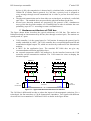
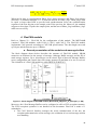
1. Hardware architecture of CAN bus
The figure shown below describes the typical architecture of CAN bus. The stations are
bidirectional and are interconnected by the bus (here through a twisted pair). The stations are
usually made of 3 parts:
CAN controller: it is the central part of a CAN station. It manages the protocol and is
usually embedded in a MCU. The CAN controller has a reception digital input RX and
a transmission digital output TX, which are not directly connected to the transmission
medium.
A MCU for the application layer. The standard IEC11898 does not give any
recommendations about the application layer.
An external component called CAN transceiver for the interface between the CAN
controller and the transmission medium. The CAN transceiver aims at shaping the
electrical signals.
Station 1
Station N
CPU
Microcontroller
CPU
Microcontroller
….
CAN controller
TX
CAN controller
RX
TX
CAN transceiver
CAN transceiver
CANH
Bus
termination
RX
CANH
Bus
termination
CAN bus
CANL
CANL
Figure 11 – Typical hardware architecture of a CAN bus
The CAN bus is differential in order to reduce the impact of electromagnetic emissions. For a
twisted pair, the line must have a 120 Ω characteristic impedance. Two signals with different
electrical level are transmitted: CANH and CANL as shown in the figure below.
34
5 e année ESE
BE électronique automobile
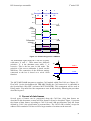
‘0’
‘1’
TX
‘1’
Recessive Dominant Recessive
bit
bit
bit
5V
0V
time
Line
voltage
3.5 V
CANH
2.5 V
1.5 V
CANL
time
Differential
voltage
5V
0.9 V
0.5 V
-1 V
time
Figure 12 – Electrical signal on a CAN bus
The transmitted signal along the CAN bus is binary
with states ’0’ and ‘1’. These states have different
priorities: ’0’ is the dominant state while ‘1’ is
recessive. This is the bus state in idle mode. The
principle of the access arbitration is based on this
difference. The connection of the different stations
connected to the bus is based on a wired AND
function.
TX
CANH
R
V+
R
CANL
TX
The MCU MPC5604B integrates a complete CAN module called FlexCAN (see Chapter 22 –
FlexCAN). On the development kit TRK-MPC5604B, the CAN transceiver is embedded in
the System Basis Chip SBC (reference MCZ33905S5EK). This component will be used in
Debug mode. You must force the component to enter in this mode by following the procedure
described in part 5.
2. Format of data frames
Several types of frames can be propagated along the CAN bus. Only data frames are
described in this document, remote and error frames will not be described. Figure 11 presents
the format of data frames, according to CAN 2.0A and 2.0B specifications. Only the frame
defined by CAN 2.0A specification is presented here. The CAN 2.0B is similar, except the
address field extended to 29 bits to offer a larger number of stations on the network.
35
5 e année ESE
BE électronique automobile
ACK
slot
CRC
delimiter
Bus
Idle
S
O
F
Address
(ID)
Arbitration
field
11 bits
R
R0,
T
R1
R
DLC
Command
field
4 bits
Data
E
O
F
CRC
Data field
CRC
0 – 8 octets
16 bits
ACK
delimiter
Int
Bus
Idle
ACK
2 bits 7 bits3 bits
Figure 13 – Format of data frame (CAN 2.0A specification)
The frame is composed of the following field:
Start of Frame bit (SOF): dominant bit emitted by any station that wants to transmit a
data frame. Once this bit is emitted, no other station will try to transmit.
The address or frame identifier (ID) field composed of the 11 bits (or 29 bits in CAN
2.0B specification) of the frame and the RTR bit (to indicate a Remote Transmission
Request frame). This field is used to determine which station is allowed to transmit.
The priority is given to the station with the ID field which starts with the largest
number of dominant bit (bit ‘0’). This field is not always used to identify the addressee
of the message. The CAN standard does not give any recommendations about the
construction of identifiers.
The RTR bit indicates if the frame type is data or remote frame.
The control field is composed of 2 reserved bits R1 and R0 for future extension of the
CAN standard. R1 can be used as IDE bit (Identifier Extension) in order to indicate if
the frame is in standard format. The 4 following bits are the Data Length Code (DLC)
field which provides the octet number of the data field within the transmitted frame.
The data field can be 0 to 8 octet long. MSB is transmitted first in each octet.
The CRC field (Cyclic Redundancy Code) is made of 15 bits and one delimiter bit.
The coding is BCH type (Bose-Chaudhuri-Hocquenghem).
The acknowledgment field is made of 2 bits. The emitter station transmits 2 recessive
bits. During the reception of the first bit (called Acknowledgement Slot), all the other
stations connected to the bus which have received a valid message must transmit a
dominant bit. The emitter station receives a dominant bit if at least one station have
receive a valid message. If one station has received an invalid message, it must
transmit an error frame.
End of Frame (EOF): this field is composed of 7 recessive bits and notifies the end of
the frame.
Interframe bit: it is a separator between 2 successive frames. It is composed of 3
recessive bits.
At the end of the frame emission, the bus enters in IDLE mode. By default, the bus state is
recessive.
36
5 e année ESE
BE électronique automobile
3. Bit time and data synchronization
The transmission of digital information requires a correct reading and interpretation of the
received signal. The sample point of the received signal must be defined precisely. The choice
of the sample point relies on a compensation of:
the delay introduced by the signal propagation along the bus and through the
electronic devices
the delay induced by arbitration and acknowledgment phases required by the protocol.
All the other source of variability of binary period (such as jitter on clock signal, loss
of synchronization)
The CAN standard proposes an organization of the bit time in several time segments in order
to define an optimal sample point.
a. Construction of the bit time
The CAN standard has defined a precise construction of the bit time in several segments in
order to compensate signal propagation delay, ensure receptor synchronization on incoming
bit stream and resynchronization of the receptor in case of variation of the clock frequency of
one station. All the stations must operate with in-phase binary clocks which have exactly the
same frequency. However, these clocks are built from the fastest clock within the system,
which is not shared by all the stations.
CAN standard define a bit time from a time base called minimum time quantum. It is the
smallest time elements considered by a station. In case of a CAN controller embedded in a
MCU, the minimum time quantum is equal to the CAN controller bus period. The time
quantum Tq is defined from this minimum time quantum and sets the time unit to build the bit
time.
The bit time is divided in 4 different segments, defined by an integer number of time quantum.
Sample point
Seg.
Sync.
Seg.
Propag.
Phase
Seg. 1
Phase
Seg. 2
1. Tq
1 to 8 Tq
1 to 8 Tq
2 to 8 Tq
Figure 14 – Structure of a bit time and organization in time quanta
b. Synchronization segment
This segment is always equal to 1 Tq. This segment is associated to the detection of a bit. If
the receptor is synchronized on the received signal accurately, the incoming binary transition
will coincide with the bit start forecast by the receptor. However, this is not true in practice,
due to loss of synchronization between the different stations connected to the bus. But the
CAN standard proposes some tricks to resynchronize the receptor and adjust the sample point.
c. Propagation segment
The signal propagation along the bus is not instantaneous. There is a certain delay due to the
finite propagation speed of the signal and the line mismatch issues. Moreover, the electronic
devices of the CAN transceiver introduce a significant delay. The binary signal setting is
delayed and so that a minimum bit time must be respected.
37
5 e année ESE
BE électronique automobile
CPU
Microcontroller
CPU
Microcontroller
CAN controller
CAN controller
Tcont
TX
Ttransc
RX
TX
CAN Transceiver
RX
CAN transceiver
CANH
Tcont
Ttransc
CANH
CAN bus
CANL
CANL
Tbus
Figure 15 – Delay induced along the CAN bus
The propagation segment aims at compensating these delays. The method suggested by the
CAN standard to define a correct value for the propagation delay consists in considering the
worst case situation: 2 stations separated by the longest cable length. The first station
transmits a recessive bit which propagates to the second station. Before this bit arrives, the
second station emits a dominant bit, which forces the bus in dominant state after a certain
delay. This dominant bit propagates to the first station. As soon as the first station receives the
dominant bit, it loses the bus arbitration immediately. The arbitration is ensured only if the
propagation segment duration is larger than the sum of all the delay, i.e the round trip time of
the signal.
Tseg propag
2
delay
d. Resynchronization – Phase errors and resynchronization
jumps
Before explaining the roles of phase segments Phase Seg. 1 and 2, we have to introduce how
CAN receptors are resynchronized. CAN transmission type is asynchronous (the bus clock is
not transmitted). The clock of the receptor is synchronized on the incoming binary stream
(from the binary transitions).
The CAN stations have different clock reference and are separated by long cables (up to
hundred of meters). In these conditions, a perfect synchronization cannot be guaranteed
between every station. Two mechanisms are defined by the CAN protocol for the
resynchronization and are not applied simultaneously:
Hardware synchronization: the rising edge instant of the incoming binary signal is
compared to the on-going bit time. If these instants are different, the bit time starting is
modified and synchronized on the incoming bit.
Resynchronization bit time: this is a software method dedicated to the compensation
of phase error, i.e. the gap between the actual rising edge of the incoming bit and its
forecast position. This phase error is introduced by the variations of frequency of each
CAN controller of the stations connected to the bus.
The following figure describes the concept of phase jumping. If the phase error remains small,
its effect can be compensated only by readjusting the position of the resynchronization
segment: a resynchronization jump is done. However, this jump is limited by the
38
5 e année ESE
BE électronique automobile
Resynchronization Jump Width (RJW). It is expressed in Time quanta, and ranged from 1 to 4
Tq.
If e RJW , then the resynchronization is similar to a hardware synchronization.
If not, the resynchronization consists in modifying the time intervals Phase Seg. 1 and Phase
Seg. 2 in order to resynchronize the bit time and readjust the sample point:
If e > RJW, the rising edge of the incoming bit falls into the propagation segment or
segment phase 1 of the current bit. The position of sample time is readjusted by
increasing the duration of segment phase 1.
If e < -RJW, the rising edge of the incoming bit falls into the propagation segment or
segment phase 2 of the previous bit. The position of sample time is readjusted by
increasing the duration of segment phase 2.
Bit incident
Incoming bit
e>RJW
e>0
Forecast bit
time
RJW
Seg.
Sync.
Seg.
Propag.
Phase
Seg. 1
Phase
Seg. 2
Bit time
attendu
RJW
RJW
Seg.
Sync.
Seg.
Propag.
Phase
Seg. 1
Phase
Seg. 2
RJW
Seg Ph1
increases
Hardware
synchro.
New Bit
time
sample
sample
sample
sample
Seg.
Sync.
Seg.
Propag.
Phase
Seg. 1
Phase
Seg. 2
Nouveau
Bit time
Seg.
Sync.
Seg.
Propag.
Phase
Seg. 2
Phase
Seg. 1
Figure 16 – Resynchronization mechanisms (left: hardware, right: bit time)
e. Phase segments 1 et 2
After the description of resynchronization mechanism, we can detail how to configure
segments Phase 1 and Phase 2. Their duration depends on RJW, which must be computed.
RJW aims at compensating the clock frequency drift of every stations. This effect is linked to
internal oscillator (effect of temperature, process dispersion) or frequency drift linked to
frequency modulation of the clock source for example. For example, the error on clock period
is expressed in percent as Error and is the sum of the tolerance of the resonant frequency of
quartz and the other source of error such as the frequency modulation applied on the clock.
The clock period varies between:
Error
Error
TCLK _ NOM 1
TCLK TCLK _ NOM 1
100
100
Error
The maximum variation of a bit time is equal to Tbit max Tbit _ nom
. The
100
resynchronization jump must compensate the worst case clock frequency variation, which
occurs when the clock period varies between both extreme values between 2 consecutive bits:
Error
RJW 2 Tbit max 2 Tbit _ nom
100
CAN standard defines another worst case situation: 29 identical bits are transmitted
successively. The CAN receiver does not detect any edge transition and desynchronization
can occur due to oscillator drift. The CAN standard prohibits that more than 29 successive
identical bits are transmitted. With this worst case situation, the resynchronization jump must
be equal to:
39
5 e année ESE
BE électronique automobile
RJW
29 2
Tbit max
58 Tbit _ nom
Error
100
When the bit time is resynchronized, Phase_Seg1 always increases and Phase_Seg2 always
decreases. A minimum duration of 1 Tq must be ensured for Phase_Seg1. Phase_Seg2 must
be equal or larger than RJW to prevent hard synchronization forces the synchronization
segment of the next bit time at the sample point of the previous bit. Moreover, the standard
suggests to let at least 2Tq after the sample point, and the sum of Phase_Seg1 and Phase_Seg2
must not exceed 8Tq.
4. FlexCAN module
Refer to Chapter 22 – FlexCAN for the configuration of this module. The MPC5604B
contains 3 FlexCAN modules, called CAN_0, CAN_1 and CAN_2. The FlexCAN module
implements CAN protocol according to CAN 2.0B specifications. The data length can reach
up 8 bytes and the data rate up to 1 Mbits/s.
a. General presentation of the module and message buffers
The block diagram shown below describes the structure of FlexCAN module. SRAM
memories are dedicated to the storage of message (Message Buffer storage) and the ID of
mask storage registers. Up to 64 messages can be stored. Each of these 64 Message Buffers
stores configuration and control data, time stamp, message ID and data to be set or received.
The 64 buffers of a FlexCAN module are called BUF[0] to BUF[63].
Figure 17 - Block diagram of FlexCAN module (Bolero512K_RM_Rev7_07_2010.pdf - p. 599)
Moreover, the 8 first Message Buffers can be configured to offer a FIFO reception structure.
The FIFO reception operation is not detailed in this document. FlexCAN is made of 3
submodules:
The CAN Protocol Interface manages the serial communication of the bus, the
reception and transmission of the messages, the validation of received message and the
error handling
40
BE électronique automobile
5 e année ESE
The Message Buffer Management manages the selection of Message Buffer for
transmission and reception
The Bus Interface Unit controls the access to the internal bus for the connection with
the CPU. The Bus Interface Unit receives the clock and the data to transmit from the
CPU and provides received data and interrupts.
The clock of the module can be derived from the bus clock or the quartz oscillator. Maskable
interrupts are generated at each reception or transmission of a message.
We detail now how works the reception / transmission of the messages rapidly. In reception
mode, the 64 Message Buffers works as a mailbox. The 64 message buffers are characterized
by programmable IDs. The Message buffers store any frames which have the same ID, i.e.
match. In transmission mode, an arbitration algorithm decides the prioritization of message
buffers to be transmitted. The prioritization is based on the message ID (+ 3 prioritization bits
PRIO for local priority) or the message buffer ordering according to the FlexCAN module
configuration. The arbitration of the prioritization of message buffer transmission is described
in the Transmission process part.
Figure 16 presents the structure of a Message Buffer. The buffer supports extend or standard
frames (29 or 11-bit identifier).
Figure 18 – Message buffer structure (Bolero512K_RM_Rev7_07_2010.pdf - p. 604)
The CODE field can be accessed by the CPU or by the module FlexCAN. It indicates the
status of the Message Buffer and if it is in reception or transmission mode. Refer to tables 225 and 22-6 (p 605) for the encoding of Message Buffers. The user or the module changes this
field to indicate that a message can be sent or a message has been sent. During transmission in
Extended mode, the bit SRR must be set to ‘1’. The bit IDE identifies the frame format
(Extended or Standard). The bit RTR set to ‘1’ indicates that the Message Buffer has to
transmit a Remote frame.
The field Length gives the length of the data (up to 8 bytes). The TIME STAMP is a copy of
the free running counter embedded in the FlexCAN module (not detailed in this document).
PRIO field gives a local priority to the Message Buffer in transmission mode (if LPRIO_EN
bit is set in MCR register). The ID field is used for frame identification. In standard mode,
only the 11 first bit are considered. The 8 DATA bytes contain the data to be transmitted or
the Data received.
b. Principle of the configuration of the FlexCAN module
The software configuration of the FlexCAN module follows this procedure:
Configuration of I/O pads
Configuration of control registers of FlexCAN module
Timing configuration (binary period and segments)
Configuration of the interrupts
Configuration of error management
Configuration of operation mode
41
BE électronique automobile
5 e année ESE
Refer to part 22-5. « Initialization/Application information » p. 642 for more information
about the programming of the FlexCAN module.
c. Configuration of I/O pads
Two I/O pads are used for one CAN bus: a TX output and a RX input. TX and RX are
alternate functions of several I/O pads. You can refer to Table 2-3 p. 45 to have a detail of the
alternate functions of each I/O pad of the MCU.
Digital pads must be configured for TX and RX pins. It is recommended to configure TX as a
open-drain output, with a medium or fast option. The RX must be configured as a digital input.
For some pins, several CAN RX can be routed (e.g. on PC11, CAN1RX and CAN4RX are
routed). It is necessary to define which CAN RX will be connected to the pad by the PSMI
registers (see chapter SIUL).
d. Configuration of the control registers
Two registers provide the general configuration of the FlexCAN module: the Module
Configuration Register (MCR) which sets global configurations of the module, and the
Control Register (CR) which controls CAN bus features of the module (some of the bits of
CR registers are detailed in timing configuration).
Let’s start with the MCR register. This register can only be changed when the FlexCAN
module is in Freeze mode.
Clearing the MDIS bit enables the FlexCAN module. Setting the FRZ bit enables the module
to enter in Freeze mode in Debug mode or when HALT bit is set. The bit NOT_RDY
indicates if the module is in Freeze or Disable mode. FRZ_ACK indicates if the module is in
Freeze mode.
The WRN_EN bit enables Warning interrupts (in TX or RX) (See error counters for more
detail about warning). The LPM_ACK indicates if the module is in Disable mode. Clearing
the bit SRX_DIS enables the self reception, i.e. if a FlexCAN module is allowed to receive a
frame that it transmits. The BCC bit allows the backward compatibility, i.e. a compatibility
with previous implementation of CAN module in older MCU. In previous modes, the
masking of identifiers cannot be done on individual Message Buffer. If the BCC bit is cleared,
the previous implementation is allowed and the masking is ensured by the registers
RXGMASK, RX14MASK and RX15MASK.
The LPRIO_EN enables the local priority to extend the ID during arbitration process. The
local priority is given by the field PRIO of the Message Buffer. The AEN bit enables the abort
of a transmitted frame. The MAXMB indicates the maximum number of Message Buffer used
in the arbitration and matching processes.
42
5 e année ESE
BE électronique automobile
Some details are now given about the CR registers (not the bit about timing configuration:
RJW, PSEG 1 and 2, and PROPSEG, and the interrupt enabled bits). The bit CLK_SRC
selects the CAN clock source, either from the crystal oscillator, or the bus clock. The clock
source is then divided by a prescaler, configured by PRESDIV. The resulted clock is used to
define the Time quanta. The bit LPB enables the loop-back mode (internal loop-back for test).
The bit SMP configures the type of sampling (one or three point). The bit LBUF defines the
ordering mechanism for Message Buffer transmission. The LOM bit enables the Listen-only
mode.
e. Configuration of bit time
The CAN bus bit-rate depends on the CAN module clock, derived from the CAN clock source
(bit CLKSRC) in CR register, and the division factor of the prescaler defined by the field
PRESDIV. The binary period or bit time is divided in several segments given in Time quata
Tq, according to:
Pr escaler value
bit time
Pr op _ Seg Time Segment 1 Time Segment 2
FCLK
bit time Tq
Pr op _ Seg
Time Segment 1 Time Segment 2
The different segments are configured by CR register. The field PROPSEG defines the
propagation segment time according to: propagation segment time Tq 1 PROPSEG .
The resynchronization jump is given by the 2 bit field RJW (from 0 to 3Tq). The fields
PSEG1 and PSEG2 define the lengths of Phase segment 1 and 2 (from 0 to 7 Tq).
f. Interrupt configuration
The module can generate up from Message Buffers and 4 interrupts due to Bus Off, Error, Tx
Warning and Rx Warning. Eight interrupt vectors are associated to a FlexCAN module.
The 4 types of interrupt can be enabled globally in CR register, with the bits BOFFMSK,
ERRMSK, TWRNMSK, RWRNMSK for Bus Off, Error, Tx and Rx Warning respectively.
The flags associated to these interrupts are in ESR register.
Moreover, each one of the Message Buffers can be an interrupt source when valid message
are transmitted or received, if its corresponding IMRH (Buffer 63 to 32) and IMRL (Buffer 31
to 0) bit is set. There is no distinction between Tx and Rx interrupts for a particular buffer,
under the assumption that the buffer is initialized for either transmission or reception. Each of
the buffers has assigned a flag bit in the IFRH (Buffer 63 to 32) and IFRL (Buffer 31 to 0)
registers. The bit is set when the corresponding buffer completes a successful
43
5 e année ESE
BE électronique automobile
transmission/reception and is cleared when the CPU writes it to ‘1’ (unless another interrupt is
generated at the same time).
The following table sums up the number of vector interrupt associated to the interrupt sources
of the three FlexCAN modules of the MCU.
Vector number
Interrupt
65
66
FlexCAN_ESR (Err_Int)
FlexCAN_ESR_Bus_off,
FlexCAN_TX_Warning,
FlexCAN_RX_Warning
FlexCAN_BUFF_00-03
FlexCAN_BUFF_04-07
FlexCAN_BUFF_08_11
FlexCAN_BUFF_12_15
FlexCAN_BUFF_16_31
FlexCAN_BUFF_32-63
FlexCAN_ESR (Err_Int)
FlexCAN_ESR_Bus_off,
FlexCAN_TX_Warning,
FlexCAN_RX_Warning
FlexCAN_BUFF_00-03
FlexCAN_BUFF_04-07
FlexCAN_BUFF_08_11
FlexCAN_BUFF_12_15
FlexCAN_BUFF_16_31
FlexCAN_BUFF_32-63
FlexCAN_ESR (Err_Int)
FlexCAN_ESR_Bus_off,
FlexCAN_TX_Warning,
FlexCAN_RX_Warning
FlexCAN_BUFF_00-03
FlexCAN_BUFF_04-07
FlexCAN_BUFF_08_11
FlexCAN_BUFF_12_15
FlexCAN_BUFF_16_31
FlexCAN_BUFF_32-63
68
69
70
71
72
73
85
86
88
89
90
91
92
93
105
106
108
109
110
111
112
113
Module
FlexCAN_0
FlexCAN_1
FlexCAN_2
g. Configuration of error management
Transmission or reception errors can occur in CAN bus and an error management strategy is
defined by CAN protocol. This strategy relies on two 8 bit error counters: one for
transmission errors, the second for reception errors. The FlexCAN module proposes the
register ECR that concatenates Rx and Tx error counters. Each time an error is detected, one
of this counter is incremented automatically (when the CAN bus is not in Freeze mode). If no
errors are detected, the counters decrement regularly. Depending on the value of the counters,
the module can be in error passive, error active or Bus-off Mode. The module enters in Busoff mode when the counters reach 255. In that case, the FlexCAN stops transmitting and waits
for 128 valid occurrences of 11 consecutive recessive bits.
44
BE électronique automobile
5 e année ESE
The error conditions and the general status of the error counters are given by the register ESR.
h. Configuration of operation modes
The FlexCAN module has 4 functional modes:
Normal mode (user or supervisor): the module is active, it receives or sends messages
normally, and the entire CAN protocol functions are activated.
Freeze mode: in this mode, no transmission or reception processes are allowed. The
module loses synchronization with the CAN bus. If FRZ bit sets, the module enters in
Freeze mode if HALT bit in MCR register is set or in debug mode.
Listen-only mode: the transmission is disabled, the module only receives messages
acknowledged by other CAN station. The module enters in this mode if the bit LOM
in MCR register is set.
Loop-back mode: an internal loop back between the transmitter output and the
receiver input is done for test purpose. The RX CAN input is ignored and the TX CAN
output is set to recessive mode. The module enters in this mode if bit LPB in MCR
register is set.
And a low power mode:
Disable mode: All the clocks are switched off. The module enters in this mode if bit
MDIS in MCR register is set, only if all current transmission or reception processes
have finished.
i. Transmission process
To ensure the transmission of a CAN frame, the CPU must prepare a Message Buffer by
following this procedure:
45
BE électronique automobile
5 e année ESE
If the MB is active (transmission pending), the ABORT code (‘1001’) must be written
in Code field of MCR register. Then read back the Code field and the IFLAG register
to check if the transmission was aborted.
Write the ID
Write the data bytes
Write the Length, Control and Code fields of the Control and Status word to activate
the MB
Once the Message Buffer is activated, it will participate into the arbitration process and finally
be transmitted according to its priority. At the end of the successful transmission, the Code
field in the Control and Status word is updated, a status flag is set in the Interrupt Flag
Register and an interrupt is generated if allowed by the corresponding Interrupt Mask Register
bit.
If the Abort feature is enabled (bit AEN in MCR register), after the interrupt flag arises for a
transmitting message buffer, the message buffer is blocked until the interrupt flag is negated
by the CPU.
The arbitration process needs to be explained. It is an algorithm that scans all the Message
Buffer memory to find the highest priority message to be transmitted. Depending on LBUF
and LPRIO_EN bits on the Control Register, the priority depends on the lowest ID, the lowest
Message Buffer number or the highest priority field. Chapter 22.4.4 gives details about
arbitration process.
Once the highest priority Message Buffer is selected, the message is transferred in a
temporary storage space called Serial Message Buffer (SMB). When a transmission
opportunity is detected on the CAN bus, the message contained in the SMB is transmitted
according to the CAN protocol specifications.
j. Reception process
To be able to receive CAN frames into the mailbox Message Buffers, the CPU must prepare
one or more Message Buffers for reception by executing the following steps:
If the Message Buffer has a pending transmission, write an ABORT code (‘1001’) to
the Code field of the MCR register to request stop the transmission. Then read back
the Code field and the IFLAG register to check if the transmission was aborted.
If the MB is already programmed as a receiver, write ‘0000’ to the Code field of the
Control and Status word to keep the Message Buffer inactive.
Write the ID.
Write ‘0100’ to the Code field of the MCR register to activate the Message Buffer.
A Message Buffer is free to receive a new frame if the Message Buffer is not locked, and if
the Code field is either EMPTY, or FULL or OVERRUN but the CPU has already serviced
the Message Buffer.
At the end of the previous step, the Message Buffer will be able to receive frames that match
the programmed ID. At the end of a successful reception, the Message Buffer is updated by
the Message Buffer Management as follows:
The received ID, Data (8 bytes at most) and Length fields are stored.
The Code field in the MCR register is updated.
A status flag is set in the Interrupt Flag Register and an interrupt is generated if
allowed by the corresponding Interrupt Mask Register bit.
46
BE électronique automobile
5 e année ESE
When an interrupt arises after reception, the CPU must:
Read the Control and Status word
Read the ID buffer
Read the data field
The reception process with the FIFO is not detailed in this document. Refer to chapter 22.4.5
of the reference manual of the MCU for the reception procedure with FIFO.
How works the matching process? The matching process is an algorithm executed by the
MBM that scans the Message Buffer memory looking for reception Message Buffers
programmed with the same ID as the one received from the CAN bus. When a frame is
received, it is temporarily stored in a hidden auxiliary Message Buffer called Serial Message
Buffer (SMB). The matching process takes place during the CRC field of the received frame.
If a matching ID is found in one of the regular Message Buffers, the contents of the SMB will
be transferred to the matched MB, except if any protocol error is detected.
If a valid message is received and if its ID is the same than the ID of several Message Buffers,
the free Message Buffer with the lowest number will receive the message. If all the Message
Buffers with the correct IDs are not free, the last matched Message Buffer is overwritten. The
OVERRUN indication is written in the Code field.
k. Reception acceptance mask
The previous part details the matching process when a valid message is received. This process
consists in finding a Message Buffer with a valid ID. It is possible to filter some Message
Buffer with acceptance filter. The register 64 bit RXIMR provides individual masking for
every 64 Message Buffers, only if BCC bit is set in MCR register. The RXIMR register can
be configured only in Freeze mode.
The FlexCAN supports another masking process based on RGXMASK, RX14MASK and
RX15MASK registers, if the BCC bit of MCR register is reset. This global reception mode is
not described in this document.
5. Implementation of the CAN bus on the starter kit TRKMPC5604B
The starter kit TRK-MPC5604B provides one SubD9 connector (JP3) to connect to a CAN
bus. This connector is routed to CANH and CANL pins of the System Basis Chip (SBC)
MCZ3390S5EK of the test board, called MCZ33905S5EK (U2). This component dedicated to
the power management and embeds also a high-speed CAN transceiver. The RX and TX pins
of this component are connected to the pins PC10 and PC11 of the MCU. PC10 is associated
to CAN1TX (alternate function AF1), while PC11 can be associated to either CAN1RX or
CAN4RX (the selection is done through the register PSMI (see SIUL)).
The CAN transceiver ensures the interface between the CAN controller and the CAN bus. The
CAN transceiver is embedded within the SBC MCZ33905. The CAN of the SBC will work
correctly in two situations: either if the SBC is forced in its own debug mode, or if the internal
watchdog of the SBC is refreshed periodically. In this document, we will detail only the
method to force the SBC in debug mode. Refer to the SBC datasheet for more information
47
5 e année ESE
BE électronique automobile
about the refresh operation of its watchdog. Several steps must be done to ensure the entry of
SBC in debug mode:
The SBC must be supplied under 12 V to activate the on-chip voltage regulator of the
CAN transceiver. On the starter kit TRK-MPC5604B, the power supply must be
provided by an external 12 V source and by placing the jumper J1 in 5-6 position. You
should verify that the pin 16 – DBG of the SBC (you can also probe that pin on the
test point TP1) is between 8 – 10 V, that the pin 22 – RST is at 5 V, and the pin 6 –
5VCAN is at 5 V (it proves that the CAN on-chip voltage regulator operates correctly).
The SBC will be used in Debug mode. In Debug mode, the CAN transceiver remains
always active. To force the component to enter in this mode, the MCU must configure
the SBC by sending the appropriate SPI commands. On the starter kit TRKMPC5604B, the module DSPI1 pins (port H) are connected to the SBC.
You can follow the procedures below to send the correct SPI command to the SBC:
void initDSPI_1(void) {
DSPI_1.MCR.R = 0x80010001;
DSPI_1.CTAR[0].R = 0x78024424;
DSPI_1.MCR.B.HALT = 0x0;
/* Exit HALT mode: go from STOPPED to RUNNING
state*/
SIU.PCR[113].R = 0x0A04;
/* MPC56xxB: Config pad as DSPI_0 SOUT output PH1*/
SIU.PCR[112].R = 0x0103;
/* MPC56xxB: Config pad as DSPI_0 SIN input - PH0 */
SIU.PSMI[8].R = 2;
/* MPC56xxB: Select PCR 112 for DSPI_1 SIN input */
SIU.PCR[114].R = 0x0A04;
SIU.PCR[115].R = 0x0A04;
*/
}
/* MPC56xxB: Config pad as DSPI_0 SCK output - PH2 */
/* MPC56xxB: Config pad as DSPI_0 PCS0 output - PH3
void ReadDataDSPI_1(void) {
uint16_t RecDataMaster = 0;
/* Data received on master SPI */
while (DSPI_1.SR.B.RFDF != 1){} /* Wait for Receive FIFO Drain Flag = 1 */
RecDataMaster = DSPI_1.POPR.R; /* Read data received by slave SPI */
DSPI_1.SR.R = 0x80020000;
/* Clear TCF, RDRF flags by writing 1 to them */
}
void Init_SBC_DBG(void)
{
vuint32_t i;
vuint32_t j = 0;
DSPI_1.PUSHR.R = 0x0001DF80; /* Read Vreg register H, clear power on flags*/
ReadDataDSPI_1();
for (i=0; i<200; i++) {
j=j+1;
}
48
BE électronique automobile
5 e année ESE
j = 0;
DSPI_1.PUSHR.R = 0x00015A00; /* Go into ‘Normal Mode’*/
ReadDataDSPI_1();
for (i=0; i<200; i++) {
j=j+1;
}
j = 0;
DSPI_1.PUSHR.R = 0x00015E90; /*Configure voltage regulator*/
ReadDataDSPI_1();
for (i=0; i<200; i++) {
j=j+1;
}
j = 0;
DSPI_1.PUSHR.R = 0x000160C0; /* Activate CAN transceiver for TX/RX*/
ReadDataDSPI_1();
for (i=0; i<200; i++) {
j=j+1;
}
}
XIV -
SPI bus and DSPI module
This chapter aims at providing some elements about hardware architecture and operation
principles of SPI bus, but also the more basic programming elements for the embedded SPI
controller of the MPC5604B. Refer to Chapter 20 – Deserial Serial Peripheral Interface for
the configuration of DSPI module.
1. Some elements about SPI protocol
The SPI is a synchronous serial communication bus which operates in full-duplex mode. The
communication is based on a master-slave protocol. Several slaves can be placed on the bus,
the selection is done through a Chip Select line.
The bus is made of 4 logical signals:
SCLK: the clock generated by the master
MOSI (Master Output, Slave Input) or Data Out: data sent by the master
MISO (Master Input, Slave Output) or Data In: data sent by the slave
CS (Chip Select): selection of the slave by the master, usually active at low state
The MOSI of the master must be connected to the MISO of the slave and vice-versa. At each
SCLK period, one bit is exchanged. When a data transfer operation is performed, data is
serially shifted by a pre-determined number of bit positions. Because the registers are linked,
data is exchanged between the master and the slave. The data that was in the master’s shift
register is now in the shift register of the slave, and vice versa. The number of bit to exchange
can vary (it must not exceed the size of shift register).
49
BE électronique automobile
5 e année ESE
Figure 19 – SPI protocol overview (Bolero512K_RM_Rev7_07_2010.pdf - p. 522)
2. Presentation of DSPI module
a. General description
The MCU embeds 3 DSPI modules called DSPI_0, DSPI_1, DSPI_2, with 6 clock and
attribute registers and 6 Chip Select per module. Each DSPI module x has the following pins:
CS0_x: peripheral chip select 0 (slave select in master mode)
CS1_x to CS3_x: peripheral chip select 1 to 3 (unused in slave mode)
CS4_x: peripheral chip select 4 (master trigger)
CS5_: peripheral chip select 5 (unused in slave mode. In master mode, it is used as a
strobe signal transmitted after CSx signal to prevent from glitches)
SIN_x: serial data in
SOUT_x: serial data out
SCK_x: serial clock
Figure 20 - Block diagram of DSPI module (Bolero512K_RM_Rev7_07_2010.pdf - p. 495)
A 16 bit shift register in master and a 16 bit shift register in slave are associated to SOUT_x,
and SIN_x signals, and form a 32 bit register.
The SPI frames can be from 4 to 16 bits long. The data to be transmitted can come from
queues stored in SRAM external to the DSPI. Host software can transfer the SPI data from the
50
BE électronique automobile
5 e année ESE
queues to a first-in first-out (FIFO) buffer. Host software can add (or push) entries to the TX
FIFO by writing to the DSPIx_PUSHR. The DSPI ignores attempts to push data to a full TX
FIFO.
The received data is stored in entries in the receive FIFO (RX FIFO) buffer. Host software
transfers the received data from the RX FIFO to memory external to the DSPI.
The DSPI has 4 modes of operation:
Master mode (DSPI initiates and control the serial communication, the pins SCK, Sout
and CS are outputs and controlled by DSPI)
Slave mode (DSPI responds to external SPI bus masters and cannot initiate
communications. The SCK and CS pin are configured as input, an internal pull-up
must be configured on CS0_x input. All transfer attributes are controlled by the bus
master, except the clock polarity, clock phase and the number of bits to transfer which
must be configured in the DSPI slave to communicate correctly.)
Module disable mode (low power mode)
Debug mode
The DSPI has two operating states: STOPPED and RUNNING. The states are independent of
DSPI configuration. The default state of the DSPI is STOPPED. In the STOPPED state no
serial transfers are initiated in master mode and no transfers are responded to in slave mode.
The STOPPED state is also a safe state for writing the various configuration registers of the
DSPI without causing undetermined results. After a reset, the DSPI module is in STOPPED
state.
b. TX Buffering and transmitting mechanisms
The data field in the executing TX FIFO entry is loaded into the shift register and shifted out
on the serial out (SOUT_x) pin. The TX FIFO functions as a buffer of SPI data and SPI
commands for transmission. SPI commands and data are added to the TX FIFO by writing to
the DSPI push TX FIFO register (DSPIx_PUSHR). TX FIFO entries can only be removed
from the TX FIFO by being shifted out or by flushing the TX FIFO. The TX FIFO counter
field (TXCTR) in the DSPI status register (DSPIx_SR) indicates the number of valid entries
in the TX FIFO. The TXCTR is updated every time the DSPI _PUSHR is written or SPI data
is transferred into the shift register from the TX FIFO.
The TX FIFO entries are removed (drained) by shifting SPI data out through the shift register.
Entries are transferred from the TX FIFO to the shift register and shifted out as long as there
are valid entries in the TX FIFO. Every time an entry is transferred from the TX FIFO to the
shift register, the TX FIFO counter is decremented by one. At the end of a transfer, the TCF
bit in the DSPIx_SR is set to indicate the completion of a transfer. The TX FIFO is flushed by
writing a ‘1’ to the CLR_TXF bit in DSPIx_MCR. If an external SPI bus master initiates a
transfer with a DSPI slave while the slave’s DSPI TX FIFO is empty, the transmit FIFO
underflow flag (TFUF) in the slave’s DSPIx_SR is set.
51
BE électronique automobile
5 e année ESE
Figure 21 – Structure of the TX FIFO and associated counter
(Bolero512K_RM_Rev7_07_2010.pdf - p. 545)
c. RX buffering and receiving mechanisms
The RX FIFO functions as a buffer for data received on the SIN pin. The RX FIFO holds four
received SPI data frames. SPI data is added to the RX FIFO at the completion of a transfer
when the received data in the shift register is transferred into the RX FIFO. SPI data is
removed (or popped) from the RX FIFO by reading the DSPIx_POPR register. RX FIFO
entries can only be removed from the RX FIFO by reading the DSPIx_POPR or by flushing
the RX FIFO. The RX FIFO counter field (RXCTR) in the DSPI status register (DSPIx_SR)
indicates the number of valid entries in the RX FIFO. The RXCTR is updated every time the
DSPI _POPR is read or SPI data is copied from the shift register to the RX FIFO.
The RX FIFO is filled with the received SPI data from the shift register. While the RX FIFO
is not full, SPI frames from the shift register are transferred to the RX FIFO. Every time an
SPI frame is transferred to the RX FIFO, the RX FIFO counter is incremented by one. If the
RX FIFO and shift register are full and a transfer is initiated, the RFOF bit in the DSPIx_SR
is set indicating an overflow condition. Depending on the state of the ROOE bit in the
DSPIx_MCR, the data from the transfer that generated the overflow is ignored or put in the
shift register. If the ROOE bit is set, the incoming data is put in the shift register. If the ROOE
bit is cleared, the incoming data is ignored.
Host software can remove (pop) entries from the RX FIFO by reading the DSPIx_POPR. A
read of the DSPIx_POPR decrements the RX FIFO counter by one. Attempts to pop data from
an empty RX FIFO are ignored, the RX FIFO counter remains unchanged. The data returned
from reading an empty RX FIFO is undetermined.
d. Transfer attributes
The transfer attributes define the baud rate, the clock polarity, the delays between clock edge
and CS and data sampling… In master mode, they define SCK signal properties. In Slave
mode, the transfer attributes of DSPI must be the same than the Master transfer attribute to
ensure a correct reception.
The DSPI module contains 6 CTAR register which defines the transfer attributes. The SPI
slave mode transfer attributes are set in the DSPIx_CTAR0.
The SCK_x frequency and the delay values for serial transfer are generated by dividing the
system clock frequency by a prescaler and a scaler with the option of doubling the baud rate.
The baud rate is the frequency of the serial communication clock (SCK_x). The system clock
is divided by a baud rate prescaler (defined by DSPIx_CTAR[PBR]) and baud rate scaler
(defined by DSPIx_CTAR[BR]) to produce SCK_x with the possibility of doubling the baud
52
BE électronique automobile
5 e année ESE
rate. The DBR, PBR, and BR fields in the DSPIx_CTARs select the frequency of SCK_x
using the following formula:
The CS_x to SCK_x delay is the length of time from assertion of the CS_x signal to the first
SCK_x edge.
The after SCK_x delay is the length of time between the last edge of SCK_x and the negation
of CS_x.
The delay after transfer is the length of time between negation of the CSx signal for a frame
and the assertion of the CSx signal for the next frame.
When the DSPI is the bus master, the CPOL and CPHA bits in the DSPI clock and transfer
attribute registers (DSPIx_CTARn) select the polarity and phase of the serial clock, SCK_x.
The polarity bit selects the idle state of the SCK_x. The clock phase bit selects if the data on
SOUT_x is valid before or on the first SCK_x edge. In slave mode, clock polarity, clock
phase and number of bits to transfer must be identical for the master device and the slave
device to ensure proper transmission.
See 20.8.5 chapter for schematic of SPI transfer for different clock polarity.
e. Interrupts
The DSPI has five conditions that can generate interrupt requests:
End of transfer queue has been reached (flag EOQF): it indicates that the end of a
transmit queue is reached. The end of queue request is generated when the EOQ bit in
the executing SPI command is asserted and the EOQF_RE bit in the DSPIx_RSER is
set.
Current frame transfer is complete (flag TCF): it indicates the end of the transfer of a
serial frame. The transfer complete request is generated at the end of each frame
transfer when the TCF_RE bit is set in the DSPIx_RSER.
TX FIFO underflow has occurred (flag TFUF): it indicates that an underflow
condition in the TX FIFO has occurred. If an external SPI bus master initiates a
transfer with a DSPI slave while the slave’s DSPI TX FIFO is empty, the transmit
FIFO underflow flag (TFUF) in the slave’s DSPIx_SR is set. If the TFUF bit is set
while the TFUF_RE bit in the DSPIx_RSER is set, an interrupt request is generated.
RX FIFO overflow has occurred (flag RFOF): it indicates that an overflow condition
in the RX FIFO has occurred. A receive FIFO overflow request is generated when RX
FIFO and shift register are full and a transfer is initiated. The RFOF_RE bit in the
DSPIx_RSER must be set for the interrupt request to be generated. Depending on the
state of the ROOE bit in the DSPIx_MCR, the data from the transfer that generated the
overflow is either ignored or shifted in to the shift register. If the ROOE bit is set, the
53
BE électronique automobile
5 e année ESE
incoming data is shifted in to the shift register. If the ROOE bit is negated, the
incoming data is ignored.
FIFO overrun has occurred (flag TFUF or RFOF): it indicates that at least one of the
FIFOs in the DSPI has exceeded its capacity. The FIFO overrun request is generated
by logically OR’ing together the RX FIFO overflow and TX FIFO underflow signals.
3. Configuration of the DSPI module
a. Module configuration
The module configuration is ensured by the DSPIx_MCR register.
The bit MSTR configures the module in Master (‘1’) or Slave (‘0’) mode. The MDIS bit
allows the module disable mode entry. The FRZ bit stops SPI transfer when the device enters
in debug mode. The bit HALT provides a mechanism for software to start (‘0’) and stop (‘1’)
DSPI transfer: transition from STOPPED to RUNNING mode. The bits DIS_TXF and
DIS_RXF disable RX and TX FIFO. The bits CLR_TXF and CLR_RXF clear or flush the TX
or RX FIFO by clearing the associated counter. See MCU datasheet for details about the other
bits.
b. Clock and transfer attributes
The DSPI modules each contain six clock and transfer attribute registers (DSPIx_CTARn)
which are used to define different transfer attribute configurations. Each DSPIx_CTAR
controls the frame size, the Baud rate and transfer delay values, the clock phase and polarity
and defines if MSB or LSB is considered as first bit. Do not write in this register in
RUNNING mode (HALT = 0).
In slave mode, DSPIx_CTAR0 is used to set the slave transfer attributes. When the DSPI is
configured as an SPI master, the CTAS field in the command portion of the TX FIFO entry
selects which of the DSPIx_CTAR registers is used on a per-frame basis.
54
BE électronique automobile
5 e année ESE
The field FMSZ defines the frame size (from 4 to 16). CPOL bit defines the clock polarity, i.e.
the inactive state of SCLK. CPHA defines the clock phase, i.e. which SCK edge causes the
data to change or to be captured. The bit LSBFE defines if the LSB or MSB is transferred first.
The baud rate depends on DBR, PBR and BR bit fields (see datasheet for more information
about computation of bit rate). Depending on DBR, PBR and CPHA, duty cycle of SCLK is
changed (see Table 20-6).
The fields PCSSCK, PASC, PDT, CSSCK, ASC and DT define different delays between
either SCK, CS and data.
c. TX FIFO writing
Data are written by software in TX FIFO by the DSPIx_PUSHR register. Data written in this
register are written in TX FIFO. This register contains command bits and data (16 bits). The
field CTAS defines which CTAR register is used for clock and transfer attributes. The bit
PCSx defines if signal CSx is asserted during transfer.
The data in TX FIFO are visible in registers DSPIx_TXFRn (n from 0 to 3). They are readonly registers and cannot be modified.
d. RX FIFO writing
Received data can be read by software in TX FIFO by the DSPIx_POPR register. This
register contains only received data (16 bits). Once the RX FIFO is read, the read data pointer
is moved to the next entry in the RX FIFO. Therefore, read DSPIx_POPR only when you
need the data.
55
BE électronique automobile
5 e année ESE
The data in RX FIFO are visible in registers DSPIx_RXFRn (n from 0 to 3). They are readonly registers and cannot be modified.
e. Interrupt configuration and status
The DSPIx_RSER enables flag bits (see part 2.e of this chapter for details bout these flags) in
the DSPIx_SR to generate interrupt requests. Do not write to the DSPIx_RSER while the
DSPI is running.
The status of the module is indicated by flag bits in status register DSPIx_SR. They are set by
hardware and reflect the state of DSPI module. They can be cleared by software only by
writing ‘1’.
TCF flag indicates that a transfer is completed, i.e. all bits in a frame have been shifted out.
EOQF flag indicates that the last entry in queue transmission is ongoing. The flag TFFF
indicates that the TX FIFO is not full and be filled. It is cleared by software or when the FIFO
is full.
RFDF flag indicates the the RX FIFO is not empty and the received data can be drained in
DSPIx_POPR register. The flags TFUF and RFOF reflect TX FIFO underflow and RX FIFO
overflow conditions.
The bit TXRXS indicates that TX and RX operation are enabled (RUNNING state) or
disabled (STOPPED mode). TXCTR and RXCTR are TX and RX FIFO counter.
56
BE électronique automobile
5 e année ESE
TXNXTPTR indicates which entry in TX FIFO will be transmitted during the next transfer.
POPNXTPTR contains a pointer to the RX FIFO entry that is returned when the
DSPIx_POPR is read. The POPNXTPTR is updated when the DSPIx_POPR is read.
57