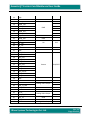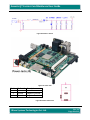
1
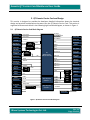
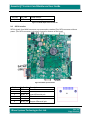
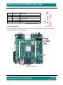
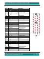
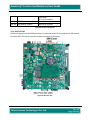
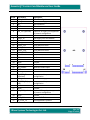
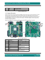
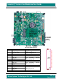
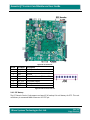
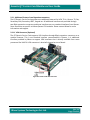
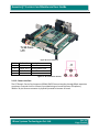
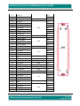
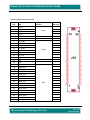
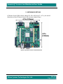
Generic Q7 Carrier Card Hardware User Guide Rainbow-G7D Generic Q7 Carrier Card Hardware User Guide iWave Systems Technologies Pvt. Ltd. Rev 1.0 Page 1 of 69 Generic Q7 Carrier Card Hardware User Guide Document Revision History Revision 1.0 Date Description 16 Mar 2012 Initial Release Version th Authors Raghavendra C PROPRIETARY NOTICE: This document contains proprietary material for the sole use of the intended recipient(s). Do not read this document if you are not the intended recipient. Any review, use, distribution or disclosure by others is strictly prohibited. If you are not the intended recipient (or authorized to receive for the recipient), you are hereby notified that any disclosure, copying distribution or use of any of the information contained within this document is STRICTLY PROHIBITED. Thank you. “iWave Systems Tech. Pvt. Ltd.” iWave Systems Technologies Pvt. Ltd. Rev 1.0 Page 2 of 69 Generic Q7 Carrier Card Hardware User Guide Table of Contents 1. INTRODUCTION ............................................................................................................. 8 1.1 1.2 1.3 1.4 1.5 2. PURPOSE ............................................................................................................................ 8 QSEVEN OVERVIEW .............................................................................................................. 8 Q7 GENERIC CARRIER CARD FEATURES .................................................................................... 8 Q7 GENERIC CARRIER CARD KIT ACCESSORIES .......................................................................... 11 LIST OF ACRONYMS ............................................................................................................ 11 Q7 GENERIC CARRIER CARD AND DESIGN................................................................................ 13 2.1 Q7 GENERIC CARRIER CARD BLOCK DIAGRAM ......................................................................... 13 2.2 QSEVEN MXM CONNECTOR ................................................................................................ 14 2.2.1 Mechanical Dimensions of Qseven CPU Module...................................................... 14 2.2.2 MXM Connector Pin Out ........................................................................................... 15 2.3 SD/MMC CARD SLOT ........................................................................................................ 19 2.4 DEBUG CONNECTORS .......................................................................................................... 20 2.4.1 9-Pin D-Sub Debug UART .......................................................................................... 20 2.4.2 JTAG Connector......................................................................................................... 22 2.5 GIGABIT ETHERNET & USB HOST0 & 2 INTERFACE ................................................................. 24 2.6 USB HOST4...................................................................................................................... 25 2.7 USB OTG ........................................................................................................................ 26 2.8 SATA0 INTERFACE ............................................................................................................. 28 2.9 SATA1 INTRAFCE............................................................................................................... 29 2.10 CAN0 INTERFACE .............................................................................................................. 30 2.11 HDMI INTERFACE .............................................................................................................. 31 2.12 AC’97 INTERFACE .............................................................................................................. 32 2.13 PCIE0 INTERFACE............................................................................................................... 34 2.14 MINI PCIE SLOT ................................................................................................................ 36 2.15 DISPLAY LVDS INTERFACE ................................................................................................... 39 2.16 7`` RESISTIVE TOUCH LCD INTERFACE .................................................................................... 43 2.17 7`` CAPACITIVE TOUCH LCD INTERFACE (OPTIONAL) ................................................................. 45 2.18 SDIO WI-FI (OPTIONAL)..................................................................................................... 48 2.19 SPI HEADER ...................................................................................................................... 49 2.20 RTC BATTERY.................................................................................................................... 50 2.21 ADDITIONAL FEATURES FROM EXPANSION CONNECTORS ............................................................ 51 2.21.1 VGA Connector (Optional) .................................................................................... 51 2.21.2 TV-In Interface ...................................................................................................... 52 2.21.3 Camera Interface .................................................................................................. 53 2.21.4 TV-Out Interface (Optional) .................................................................................. 55 iWave Systems Technologies Pvt. Ltd. Rev 1.0 Page 3 of 69 Generic Q7 Carrier Card Hardware User Guide 2.21.5 Secondary CAN (Optional) .................................................................................... 56 2.21.6 Secondary UART .................................................................................................... 57 2.21.7 Keypad interface ................................................................................................... 58 2.22 EXPANSION CONNECTORS .................................................................................................... 59 2.23 POWER SUPPLY.................................................................................................................. 65 2.23.1 Power Jack ............................................................................................................ 65 3. MECHANICAL DETAILS .................................................................................................. 67 4. REFERENCE .................................................................................................................. 68 5. TECHNICAL SUPPORT ................................................................................................... 69 iWave Systems Technologies Pvt. Ltd. Rev 1.0 Page 4 of 69 Generic Q7 Carrier Card Hardware User Guide Table of Figures FIGURE 1: Q7 GENERIC CARRIER CARD BLOCK DIAGRAM........................................................................... 13 FIGURE 2: MECHANICAL SPEC OF QSEVEN CPU MODULE .......................................................................... 15 FIGURE 3: SD/MMC CARD SLOT ......................................................................................................... 19 FIGURE 4: SD/MMC CONNECTOR PIN OUT ........................................................................................... 20 FIGURE 5: DEBUG PORT SELECTION ........................................................................................................ 20 FIGURE 6: UART (DB9) CONNECTOR.................................................................................................... 21 FIGURE 7: PIN D-SUB DEBUG UART CONNECTOR PIN OUT ....................................................................... 22 FIGURE 8: JTAG CONNECTOR .............................................................................................................. 23 FIGURE 9: JTAG CONNECTOR PIN OUT .................................................................................................. 23 FIGURE 10: RJ45 (GBE) & USB HOST0 & HOST2 CONNECTOR ................................................................ 24 FIGURE 11: RJ45 MAGJACK WITH DUAL USB TYPE-A CONNECTOR PIN OUT ................................................ 25 FIGURE 12: USB HOST4 CONNECTORS .................................................................................................. 26 FIGURE 13: USB HOST4 CONNECTOR PIN OUT ....................................................................................... 26 FIGURE 14: USB1 OTG CONNECTOR .................................................................................................... 27 FIGURE 15: USB1 OTG CONNECTOR PIN OUT ....................................................................................... 27 FIGURE 16: SATA0 22PIN CONNECTOR ................................................................................................. 28 FIGURE 17: SATA0 22PIN CONNECTOR PIN OUT .................................................................................... 29 FIGURE 18: SATA1 7PIN CONNECTOR ................................................................................................... 29 FIGURE 19: SATA1 7PIN CONNECTOR PIN OUT ...................................................................................... 30 FIGURE 20: CAN 9-PIN D-SUB CONNECTOR ........................................................................................... 30 FIGURE 21: CAN 9-PIN D-SUB CONNECTOR PIN OUT .............................................................................. 30 FIGURE 22: HDMI PORT..................................................................................................................... 31 FIGURE 23: HDMI PORT PIN OUT ........................................................................................................ 32 FIGURE 24: AUDIO JACK...................................................................................................................... 33 FIGURE 25: AUDIO OUT JACK PIN OUT ................................................................................................. 33 FIGURE 26: MIC IN JACK PIN OUT ........................................................................................................ 34 FIGURE 27: PCIE0 X1 SLOT ................................................................................................................. 34 FIGURE 28: PCIE0 X1 SLOT PIN OUT .................................................................................................... 36 FIGURE 29: MINI PCIE SLOT ................................................................................................................ 36 FIGURE 30: MINI PCIE SLOT PIN OUT ................................................................................................... 38 FIGURE 31: SIM SLOT PIN OUT ............................................................................................................ 39 FIGURE 32: LVDS0 CONNECTORS ......................................................................................................... 39 FIGURE 33: LVDS0 CONNECTOR PIN OUT.............................................................................................. 40 FIGURE 34: LVDS0 BACKLIGHT CONNECTOR PIN OUT .............................................................................. 40 FIGURE 35: LVDS1 CONNECTORS ......................................................................................................... 41 FIGURE 36: LVDS1 CONNECTOR PIN OUT.............................................................................................. 42 FIGURE 37: LVDS1 BACKLIGHT CONNECTOR PIN OUT .............................................................................. 42 FIGURE 38: 7`` RESISTIVE LCD CONNECTOR ........................................................................................... 43 iWave Systems Technologies Pvt. Ltd. Rev 1.0 Page 5 of 69 Generic Q7 Carrier Card Hardware User Guide FIGURE 39: 7`` RESISTIVE LCD CONNECTOR PIN OUT ............................................................................... 44 FIGURE 40: RESISTIVE TOUCH CONNECTOR PIN OUT ................................................................................ 45 FIGURE 41: 7`` CAPACITIVE TOUCH LCD CONNECTOR .............................................................................. 45 FIGURE 42: 7`` CAPACITIVE TOUCH LCD CONNECTOR PIN OUT .................................................................. 47 FIGURE 43: CAPACITIVE TOUCH CONNECTOR PIN OUT .............................................................................. 47 FIGURE 44: SDIO WI-FI MODULE CONNECTOR ...................................................................................... 48 FIGURE 45: SDIO WI-FI MODULE CONNECTOR PIN OUT .......................................................................... 49 FIGURE 46: SPI CONNECTOR ............................................................................................................... 50 FIGURE 47: SPI CONNECTOR PIN OUT ................................................................................................... 50 FIGURE 48: 15-PIN D-SUB VGA CONNECTOR ........................................................................................ 51 FIGURE 49: 15-PIN D-SUB VGA CONNECTOR PIN OUT ............................................................................ 52 FIGURE 50: TV-IN CONNECTOR ............................................................................................................ 53 FIGURE 51: TV-IN CONNECTOR PIN OUT ............................................................................................... 53 FIGURE 52: CAMERA CONNECTOR ......................................................................................................... 54 FIGURE 53: CAMERA CONNECTOR PIN OUT ............................................................................................ 55 FIGURE 54: TV-OUT CONNECTOR ......................................................................................................... 55 FIGURE 55: TV-OUT CONNECTOR PIN OUT ............................................................................................ 56 FIGURE 56: SECONDARY CAN CONNECTOR ............................................................................................ 56 FIGURE 57: SECONDARY CAN CONNECTOR PIN OUT ................................................................................ 56 FIGURE 58: SECONDARY UART CONNECTOR .......................................................................................... 57 FIGURE 59: SECONDARY UART CONNECTOR PIN OUT .............................................................................. 57 FIGURE 60: KEYPAD CONNECTOR .......................................................................................................... 58 FIGURE 61: KEYPAD CONNECTOR PIN OUT ............................................................................................. 58 FIGURE 62: EXPANSION CONNECTOR1 PIN OUT ...................................................................................... 61 FIGURE 63: EXPANSION CONNECTOR2 PIN OUT ...................................................................................... 64 FIGURE 64: POWER IN CIRCUIT............................................................................................................. 66 FIGURE 65: POWER JACK..................................................................................................................... 66 FIGURE 66: POWER JACK PIN OUT ........................................................................................................ 66 FIGURE 67: Q7 GENERIC CARRIER CARD PCB DIMENSION ........................................................................ 67 iWave Systems Technologies Pvt. Ltd. Rev 1.0 Page 6 of 69 Generic Q7 Carrier Card Hardware User Guide List of Tables TABLE 1: ACRONYMS & ABBREVIATIONS ................................................................................................ 11 TABLE 2: MXM CONNECTOR ............................................................................................................... 14 TABLE 3: MXM CONNECTOR PIN OUT................................................................................................... 15 TABLE 4: USB OTG ID SELECTION ........................................................................................................ 27 TABLE 5: EXPANSION CONNECTOR1 PIN OUT .......................................................................................... 59 TABLE 6: EXPANSION CONNECTOR2 PIN OUT .......................................................................................... 62 TABLE 7: POWER SEQUENCE TABLE ....................................................................................................... 65 iWave Systems Technologies Pvt. Ltd. Rev 1.0 Page 7 of 69 Generic Q7 Carrier Card Hardware User Guide 1. INTRODUCTION 1.1 Purpose This document is the Hardware Reference Manual for the Q7 Generic Carrier Card. This board is fully supported by iWave Systems Technologies Pvt. Ltd. This Manual includes system setup, debugging and provides detailed information on the overall design and usage of the Q7 Generic Carrier Card from a Hardware Systems perspective. 1.2 Qseven Overview The Qseven concept is an off-the-shelf, multi vendor, Single-Board-Computer that integrates all the core components of a common PC and is mounted onto an application specific carrier board. Qseven modules have a standardized form factor of 70mm x 70mm and have specified pinouts based on the high speed MXM system connector that has a standardized pinout regardless of the vendor. The Qseven module provides the functional requirements for an embedded application. These functions include, but are not limited to, graphics, sound, mass storage, network and multiple USB ports. A single ruggedized MXM connector provides the carrier board interface to carry all the I/O signals to and from the Qseven module. This MXM connector is a well known and proven high speed signal interface connector that is commonly used for high speed PCI Express graphics cards in notebooks. iWave Q7 carrier card incorporated with additional two 80pin expansion connectors to bring the non standard Qseven interfaces to carrier card associated with iWave’s Qseven CPU modules. 1.3 Q7 Generic Carrier Card Features Qseven Standard features Secure Digital I/O interface 8bit MMC/SDIO Connector Debug Connectors 9-Pin D-Sub Debug UART Connector 10-Pin JTAG Connector Gigabit Ethernet RJ45MagJack for 10/100/1000 Mbps Ethernet USB 2.0 HS USB 2.0 Standard-A Host Connector x3 HS USB 2.0 Micro USB OTG Connector iWave Systems Technologies Pvt. Ltd. Rev 1.0 Page 8 of 69 Generic Q7 Carrier Card Hardware User Guide Serial ATA 22pin SATA Connector for SATA port0 7pin SATA Connector for SATA port1 CAN 9-Pin D-Sub Connector TMDS Standard HDMI port AC’97 Audio 3.5mm Stereo Head Phone output 3.5mm Mono-Microphone input PCIExpress 1X PCIe slot/Mini PCIe Connector Mini PCIe connector 52-Pin mini PCIe connector with USB Interface (USB Port3). SIM slot provided to support 3G modules LVDS Display Interface 20pin Primary LVDS connector with 2-pin 15V output backlight connector 20pin Secondary LVDS connector with 2-pin 15V output backlight connector RGB Display Interface from primary LVDS signals 7” RGB-18bit Resistive Touch LCD interface 7” RGB-24bit Capacitive Touch LCD interface(optional) SDIO Wi-Fi (optional) On board Taiyo Yuden SDIO OEM Wi-Fi module “WYSAAVDX7” Miscellaneous 3V, Coin cell for RTC Reset Button Power On Button SPI header Additional Features from expansion connectors VGA Output (optional) iWave Systems Technologies Pvt. Ltd. Rev 1.0 Page 9 of 69 Generic Q7 Carrier Card Hardware User Guide 15-Pin D-Sub VGA Connector TV-In interface Standard RCA Connector CMOS Camera Interface 8bit CMOS camera TV-Out interface Standard RCA Connector Secondary CAN (optional) 3-pin header Secondary UART 5-pin header 4X4 Keymatrix connector 10-pin header Others Future Expansion Header (optional) 120-Pin Expansion Header Power Supply 12V, 3A Adapter Jack Indicators Red LED for Power Indication RED Reset Indicator LED Temperature Supported - 0°C to +70°C Commercial grade PCB Nano-ITX- 120 mm × 120 mm (4.7 in × 4.7 in) Note: All Optional Features will not be supported in default configuration. Please contact iWave for optional features support. iWave Systems Technologies Pvt. Ltd. Rev 1.0 Page 10 of 69 Generic Q7 Carrier Card Hardware User Guide 1.4 Q7 Generic Carrier Card kit accessories Q7 Generic Carrier Card comes with the following accessories: Q7 Generic Carrier Card RS-232 Serial Cable 12V,2A Power Adapter 1.5 List of Acronyms The following acronyms will be used throughout this document. Table 1: Acronyms & Abbreviations Acronyms ARM BPP eCSPI GB GPIO I2C IC JTAG KB LCD LDO MB Mbps MHz MMC ms MSPS PCB PUMS PWM RGB RMII ROHS Description Advanced RISC Machine Bits Per Pixel Enhanced Configurable Serial Peripheral Interface Giga Byte General Purpose Input Output Inter-Integrated Circuit Integrated Circuit Joint Test Action Group Kilo Byte Liquid Crystal Display Low Drop-Out Mega Byte Mega bits per sec Mega Hertz Multi Media Card Milli Second Milli Second Per Sample Printed Circuit board Power Up Mode Supply Pulse Width Modulation Red Green Blue Reduced Media Independent Interface Restriction of Hazardous Substances iWave Systems Technologies Pvt. Ltd. Rev 1.0 Page 11 of 69 Generic Q7 Carrier Card Hardware User Guide RTC SD SDIO SPI SSI UART USB V VGA GBE Real Time Clock Secure Digital Secure Digital Input Output Serial Peripheral Interface Synchronous Serial Interface Universal Asynchronous Receiver/Transmitters Universal Serial bus Voltage Video Graphics Array Gigabit Ethernet iWave Systems Technologies Pvt. Ltd. Rev 1.0 Page 12 of 69 Generic Q7 Carrier Card Hardware User Guide 2. Q7 Generic Carrier Card and Design This section is designed to provide the developer detailed information about the electrical design and practical considerations that went into the Q7 Generic Carrier Card. This section is organized to discuss each block in the following high level block diagram, as shown in Figure 1. 2.1 Q7 Generic Carrier Card Block Diagram 22-Pin Conn SATA Port 0 7-Pin Conn SATA Port 1 20-Pin LVDS Conn x2 40-Pin Res TP RGB LCD Conn LVDS x2 LVDS Receiver RGB-24bit Audio Jacks AC’97 CODEC +5V Input +5V Standby Input Reset Button Push Button Power Button Push Button RTC RTC Battery LVDS0 AC’97 SMBus Header PCIe3 PCIe2 PCIe Header MIC/SPKR PCIe0/PCIe1 PCIe x1 Slot Connector USB Port4 USB A-Type Conn TMDS PCIe0 Ethernet USB Port 3 Mini PCIe Connector USB Port 1 USB OTG Mico/miniAB Resistive TP Conn Touch Controller I2C Capacitive TP HDMI Conn RJ45 MagJack Q7 MXM Connector (230-pin Connector) SD Conn (8bit) SD Wi-Fi SD/MMC CAN TxRX DB9 Conn Header Header Header Camera Conn Header TV OUT/VGA USB Port 0 CAN0 Dual USB Stack Conn USB Port 2 UART SPI RS232 TxRX DB9 Conn CAN TxRX Header LPC GPIO 80 pin Expansion Connector - 1 CSI IF PWM SSI Port x 2 RS232 TxRX Video Decoder CS2 IF 80 pin Expansion Connector - 2 4x4 Matrix 50pin Cap TP 7” RGB-24bit RGB LCD Conn UARTx2 Header Header Touch Panel Conn Keymatrix Header 4 Wire Analog RGB TV IN CAN1 UART UART Power Jack +12V DC Input MAIN Figure 1: Q7 Generic Carrier Card Block Diagram iWave Systems Technologies Pvt. Ltd. Rev 1.0 Page 13 of 69 Generic Q7 Carrier Card Hardware User Guide 2.2 Qseven MXM Connector The Qseven module utilizes a 230-pin card-edge connector that is also used for PCI Express capable notebook graphics cards following the MXM specification. Therefore, this connector type is also known as a MXM connector. The MXM edge connector is the result of an extensive collaborative design effort with the industry's leading notebook manufacturers. This collaboration has produced a robust, low-cost edge connector that is capable of handling high-speed serialized signals. Table 2: MXM Connector Manufacturer Foxconn Aces Part Number Specification AS0B326-S78N-7F 88882-2D0K AS0B326-S78N-7F 88882-2Dxx Resulting height between carrier board and Qseven module 5.0mm 5.0mm Overall height of the MXM Connector 7.8mm 7.5mm 2.2.1 Mechanical Dimensions of Qseven CPU Module Below figures shows the mechanical spec of CPU modules. For more information refer Qseven spec 1.20 “Qseven-Spec_1.20.pdf” iWave Systems Technologies Pvt. Ltd. Rev 1.0 Page 14 of 69 Generic Q7 Carrier Card Hardware User Guide Figure 2: Mechanical spec of Qseven CPU Module 2.2.2 MXM Connector Pin Out Below tables shows the MXM connector Pin Out of Q7 Generic Carrier Card Table 3: MXM Connector Pin Out PIN NO 1 3 5 7 9 11 13 15 17 19 21 23 SIGNAL NAME GND GBE_MDI3GBE_MDI3+ LINK 100# ETH_TXN_GBE_MDI1ETH_TXP_GBE_MDI1+ ETH_LINK# ETH_CTREF * NC NC NC GND iWave Systems Technologies Pvt. Ltd. PIN NO 2 4 6 8 10 12 14 16 18 20 22 24 SIGNAL NAME GND GBE_MDI2GBE_MDI2+ GBE_LINK 1000# * ETH_RXN_GBE_MDI0ETH_RXP_GBE_MDI0+ ETH_ACT# SUS_S5# * SUS_S3# * PWRBTN# NC GND Rev 1.0 Page 15 of 69 Generic Q7 Carrier Card Hardware User Guide 25 27 29 31 33 35 37 39 41 43 45 47 49 51 53 55 57 59 61 63 65 67 69 71 73 75 77 79 81 83 85 87 89 91 93 95 97 GND NC SATA0_TX+ SATA0_TXSATA_ACT# SATA0_RX+ SATA0_RXGND NC SDIO_CD# SDIO_CMD SDIO_PWR# * SDIO_DAT0 SDIO_DAT2 SDIO_DAT4 SDIO_DAT6 GND AC_SYNC AC_RST# AC_BITCLK AC_SDI AC_SDO NC NC GND NC NC NC NC NC USB_2_3_OC# USB_P3USB_P3+ USB_CC USB_P1HCUSB_P1HC+ GND iWave Systems Technologies Pvt. Ltd. 26 28 30 32 34 36 38 40 42 44 46 48 50 52 54 56 58 60 62 64 66 68 70 72 74 76 78 80 82 84 86 88 90 92 94 96 98 PWGIN * RSTBTN# SATA1_TX+ SATA1_TXGND SATA1_RX+ SATA1_RXGND SDIO_CLK SDIO_LED SDIO_WP SDIO_DAT1 SDIO_DAT3 SDIO_DAT5 SDIO_DAT7 NC GND NC NC NC I2C_CLK I2C_DAT NC NC GND NC NC USB USB_P4USB_P4+ USB_0_1_OC# USB_P2USB_P2+ USB_ID USB_P0USB_P0+ GND Rev 1.0 Page 16 of 69 Generic Q7 Carrier Card Hardware User Guide 99 101 103 105 107 109 111 113 115 117 119 121 123 125 127 129 131 133 135 137 139 141 143 145 147 149 151 153 155 157 159 161 163 165 167 169 171 LVDS_A0+ LVDS_A0LVDS_A1+ LVDS_A1LVDS_A2+ LVDS_A2LVDS_PPEN LVDS_A3+ LVDS_A3GND LVDS_A_CLK+ LVDS_A_CLKLVDS_BLT_CTRL_GP_PWM_OUT0 LVDS_DID_DAT_GP_I2C_DAT LVDS_DID_CLK_GP_I2C_CLK CAN0_TXD TMDS_CLK+_SDVO_BCLK+ TMDS_CLK-_SDVO_BCLKGND TMDS_LANE1+_SDVO_GREEN+ TMDS_LANE1-_SDVO_GREENGND TMDS_LANE0+_SDVO_BLUE+ TMDS_LANE0-_SDVO_BLUEGND TMDS_LANE2+_SDVO_RED+ TMDS_LANE2-_SDVO_REDHDMI_HPD# PCIe_CLK_REF+ PCIe_CLK_REFGND NC NC GND NC NC NC iWave Systems Technologies Pvt. Ltd. 100 102 104 106 108 110 112 114 116 118 120 122 124 126 128 130 132 134 136 138 140 142 144 146 148 150 152 154 156 158 160 162 164 166 168 170 172 LVDS_B0+ LVDS_B0LVDS_B1+ LVDS_B1LVDS_B2+ LVDS_B2LVDS_BLEN LVDS_B3+ LVDS_B3GND LVDS_B_CLK+ LVDS_B_CLKRSVD2 LVDS_BLC_DAT LVDS_BLC_CLK CAN0_RXD NC NC GND NC NC GND NC NC GND HDMI_SDVO_CTL_DAT HDMI_SDVO_CTL_CLK NC PCIe_WAKE# NC GND NC NC GND NC NC NC Rev 1.0 Page 17 of 69 Generic Q7 Carrier Card Hardware User Guide 173 175 177 179 181 183 185 187 189 191 193 PCIE1_TX+ PCIE1_TXNC PCIE0_TXPCIE0_TXGND NC NC NC NC VCC_RTC PCIE1_RX+ PCIE1_RXNC PCIE0_RX+ PCIE0_RXGND NC NC NC NC GP_PWM_OUT2 (Connected to Secondary LVDS Backlight Control) * 195 NC 196 NC 197 GND 198 GND 199 SPI_MOSI 200 SPI_CS0# 201 SPI_MISO 202 SPI_CS1# 203 SPI_SCK 204 MFG4_JTAG_TRST# 205 VCC_5VA 206 VCC_5VA 207 MFG0_JTAG_TCK 208 MFG2_JTAG_TDI 209 MFG1_JATG_TDO 210 MFG3_JTAG_TMS 211 VCC_5V_CPU 212 VCC_5V_CPU 213 VCC_5V_CPU 214 VCC_5V_CPU 215 VCC_5V_CPU 216 VCC_5V_CPU 217 VCC_5V_CPU 218 VCC_5V_CPU 219 VCC_5V_CPU 220 VCC_5V_CPU 221 VCC_5V_CPU 222 VCC_5V_CPU 223 VCC_5V_CPU 224 VCC_5V_CPU 225 VCC_5V_CPU 226 VCC_5V_CPU 227 VCC_5V_CPU 228 VCC_5V_CPU 229 VCC_5V_CPU 230 VCC_5V_CPU Note *: Denotes Optional features, not supported in default configuration. iWave Systems Technologies Pvt. Ltd. 174 176 178 180 182 184 186 188 190 192 194 Rev 1.0 Page 18 of 69 Generic Q7 Carrier Card Hardware User Guide 2.3 SD/MMC Card Slot The SD/MMC Card Connector (J5) is connected to the Secure Digital I/O interface of the MXM connector. This card socket will support up to a 8-bit data transfer. It supports card detect feature, by default card detect pin is high after inserting card to the socket this pin should go low for proper card detection. The main power for the Card Socket is 3.3V. The SD Card slot can be configured as SD or MMC card operation. The SD Card Slot supports full 8-bit parallel data transfers and can support SDIO cards (Wi-Fi, BT, etc) designed to fit in a standard SD card slot. SD/MMC slot is physically located on top of the board. Figure 3: SD/MMC Card Slot iWave Systems Technologies Pvt. Ltd. Rev 1.0 Page 19 of 69 Generic Q7 Carrier Card Hardware User Guide Pin No 1 2 3 4 5 6 7 8 9 10 11 12 13 14 15 Pin Details SDIO _WP SDIO _CD# SDIO_DAT1 SDIO_DAT0 SDIO_DAT7 GND SDIO_DAT6 SDIO _CLK SD_3V3 VSS SDIO_DAT5 SDIO_CMD SDIO_DAT4 SDIO_DAT3 SDIO_DAT2 Description Write Protect Card Detect Signal Data Line (bit1) Data Line (bit0) Data Line (bit7) Ground Data Line (bit6) Clock Supply Voltage Ground Data Line (bit5) Command Response Data Line (bit4) Data Line (bit3) Data Line (bit2) Figure 4: SD/MMC Connector Pin Out 2.4 Debug Connectors Q7 Generic Carrier Card provides a 9-Pin D-Sub Debug UART Connector and JTAG connector for debugging. Both debug interfaces are sharing same signals from MXM connector, since MUX select line is used to select either UART or JTAG. Q7 Generic Carrier Card provided jumper option (J62) to select Debug ports. For further information on these signals refer section “Manufacturing Signals” of Qseven spec R1.20. In default jumper will be open and UART will be supported. J62 Jumper Position Open Close Debug Port UART Port JTAG Port Figure 5: Debug port selection 2.4.1 9-Pin D-Sub Debug UART UART will be used for Debug purpose. This is not the full functional UART and supports only Serial TX and RX signals. External RS232 Transceiver will be used to convert the Processor CMOS UART Transmit signal into RS232 signals at the driver section and convert the RS232 receive signals into CMOS signals at the Receiver section. This RS232 signals will be connected to 9-Pin iWave Systems Technologies Pvt. Ltd. Rev 1.0 Page 20 of 69 Generic Q7 Carrier Card Hardware User Guide D-Sub Debug UART Connector which is physically located on top of the board for external debug access. Figure 6: UART (DB9) Connector iWave Systems Technologies Pvt. Ltd. Rev 1.0 Page 21 of 69 Generic Q7 Carrier Card Hardware User Guide Pin No A1 A2 A3 A4 A5 A6 A7 A8 A9 M1,M2, M3,M4 Pin Details NC MFG2_JTAG_TDI MFG1_JATG_TDO NC GND NC NC NC NC DSUB_SHLD_GND Description No Connection Receive Data to CPU Transmit Data from CPU Data Transmit Ready Ground Data Set Ready Request to Send Clear to Send No Connection Shield Ground M4 M3 M1 M2 Figure 7: Pin D-Sub Debug UART Connector Pin Out 2.4.2 JTAG Connector A 10-pin JTAG connector is provided on the Q7 Generic Carrier Card. Logic signals to the JTAG connector are depends on the Qseven CPU manufactures. JTAG connector is physically located on bottom of the board. iWave Systems Technologies Pvt. Ltd. Rev 1.0 Page 22 of 69 Generic Q7 Carrier Card Hardware User Guide Figure 8: JTAG Connector Pin No 1 2 3 4 5 6 7 8 9 10 Pin Details VCC_3V3 GND VCC_3V3 MFG4_JTAG_TRST# MFG0_JTAG_TCK MFG2_JTAG_TDI MFG1_JATG_TDO MFG3_JTAG_TMS GND GND Description Supply Voltage Ground Supply Voltage Test Reset Signal Test Clock Test Data Input Test Data Output Test Mode Select Supply Voltage Ground Figure 9: JTAG Connector Pin Out iWave Systems Technologies Pvt. Ltd. Rev 1.0 Page 23 of 69 Generic Q7 Carrier Card Hardware User Guide 2.5 Gigabit Ethernet & USB HOST0 & 2 Interface Ethernet, USB Host0 & 2 interfaces are shared stacked connector. GBE signals from MXM connector is connected to RJ45 magnetic connector (top), with LED indicators. RJ45 Ethernet connector is physically located on top of the board. Similarly USB HOST0 & USB HOST2 interfaces from MXM connector are connected to bottom and middle port respectively. GBE connector will work for both 10/100 & 10/100/1000 Mbps Ethernet operation. Figure 10: RJ45 (GBE) & USB Host0 & Host2 Connector Pin No 1 2 3 4 5 6 7 8 9 10 Pin Details GND ETH_RXP_GBE_MDI0+ ETH_RXN_GBE_MDI0ETH_TXP_GBE_MDI1+ ETH_TXN_GBE_MDI1RCT GBE_MDI2+ GBE_MDI2GBE_MDI3+ GBE_MDI3- Description Ground Media Dependent Interface (MDI) differential pair 0 Media Dependent Interface (MDI) differential pair 1 Ref Voltage(VCC_3V3) Media Dependent Interface (MDI) differential pair 2 Media Dependent Interface (MDI) differential pair 3 iWave Systems Technologies Pvt. Ltd. Rev 1.0 Page 24 of 69 Generic Q7 Carrier Card Hardware User Guide 11 12 13 14 S5,S6,S7,S8 15 A1 A2 A3 A4 S1,S2 B1 B2 B3 B4 S3,S4 LINK 100# VCC_3V3 ETH_LINK# VCC_3V3 Shield Ground ETH_ACT# USB_VBUS0 USB_P0USB_P0+ Ground Shield Ground USB_VBUS2 USB_P2USB_P2+ Ground Shield Ground LED1 Cathode LED1 Anode LED1 Cathode LED1 Anode Shield Ground Ethernet LED1 Cathode USB0 5V Power (Bottom) USB0 Data negative (Bottom) USB0 Data Positive(Bottom) USB0 Ground (Bottom) Shield Ground (Bottom) USB2 5V Power (Top) USB2 Data negative (Top) USB2 Data Positive (Top) USB2 Ground (Top) Shield Ground USB2 (Top) Figure 11: RJ45 Magjack with Dual USB Type-A Connector Pin Out 2.6 USB Host4 USB Host4 signals from the MXM connector is connected to standard USB Type-A connector. USB Host4 connector is physically located on top of the board. iWave Systems Technologies Pvt. Ltd. Rev 1.0 Page 25 of 69 Generic Q7 Carrier Card Hardware User Guide Figure 12: USB Host4 Connectors Pin No 1 2 3 4 S1,S2,S3,S4 Pin Details USB_VBUS4 USB_P4USB_P4+ Ground Shield Ground Description USB4 5V Power USB4 Data negative USB4 Data Positive USB4 Ground Shield Ground Figure 13: USB Host4 Connector Pin Out 2.7 USB OTG USB port1 OTG signals from MXM connector is connected to USB micro (Optional mini-AB) connector. USB port1 supports OTG full functionality. To support USB OTG full functionality jumper (J22) option is provided for USB-ID pin, either proper Host and Device cable can be used or Jumper can be used to configure the port. USB1 OTG connector is physically located on top of the board. iWave Systems Technologies Pvt. Ltd. Rev 1.0 Page 26 of 69 Generic Q7 Carrier Card Hardware User Guide Table 4: USB OTG ID Selection J22 Jumper Position Open Close USB OTG Functionality USB Device USB Host Figure 14: USB1 OTG Connector Pin No 1 2 3 4 Pin Details USB_VBUS1 USB_P1HCUSB_P1HC+ USB ID 5 Ground S1,S2,S3,S4 Shield Ground Description USB1 5V Power USB1 Data negative USB1 Data Positive USD ID signal Open(float): Device USB1 Ground Shield Ground Figure 15: USB1 OTG Connector Pin Out iWave Systems Technologies Pvt. Ltd. Rev 1.0 Page 27 of 69 Generic Q7 Carrier Card Hardware User Guide 2.8 SATA0 Interface SATA0 signals from MXM connector are connected to standard 22pin SATA connector with power. 22pin SATA connector is physically located on top of the board. Figure 16: SATA0 22pin Connector Pin No S1 S2 S3 S4 S5 S6 s7 P1,P2,P3 P4,P5,P6 P7,P8,P9 P10,P11,P12 P13,P14,P15 Pin Details GND SATA0_TX+ SATA0_TX GND SATA0_RX SATA0_RX+ GND VCC_3V3 GND VCC_5V GND VCC_12V Description Ground Serial ATA channel0, Receive Input differential pair. Ground Serial ATA channel0, Transmit Output differential pair. Ground 3.3V Power Supply(1000mA) Ground 5V Power Supply(1000mA) Ground 12V Power Supply(350mA) iWave Systems Technologies Pvt. Ltd. Rev 1.0 Page 28 of 69 Generic Q7 Carrier Card Hardware User Guide SH1,SH2 M1,M2 SH_GND NC Shield Ground Mechanical Support Figure 17: SATA0 22pin Connector Pin Out 2.9 SATA1 Intrafce SATA1 signals from MXM connector are connected to standard 7pin SATA connector without power. 7pin SATA connector is physically located on bottom of the board. Figure 18: SATA1 7pin Connector Pin No 1 2 3 4 5 6 Pin Details GND SATA1_TX+ SATA1_TX GND SATA1_RX SATA1_RX+ Description Ground Serial ATA channel1, Receive Input differential pair. Ground Serial ATA channel1, Transmit Output differential pair. iWave Systems Technologies Pvt. Ltd. Rev 1.0 Page 29 of 69 Generic Q7 Carrier Card Hardware User Guide 7 M1,M2 GND NC Ground Mechanical Support Figure 19: SATA1 7pin Connector Pin Out 2.10 CAN0 Interface CAN Signals TXD and RXD signals from MXM connector is connected to CAN transceiver and to 9-Pin D-Sub connector. CAN 9-pin D-Sub connector is physically located on top of the board. Figure 20: CAN 9-pin D-Sub Connector Pin No B1 B2 B3 B4 B5 B6 B7 B8 B9 M1,M2, M3,M4 Pin Details NC CAN0L GND NC CAN_SHLD_GND GND CAN0H NC VCC_12V DSUB_SHLD_GND Description No Connection CAN Differential Low Side Ground No Connection CAN Shield Ground Ground CAN Differential High Side No Connection 12V Power supply Shield Ground M4 M4 M3 M4 M3 M1 M2 Figure 21: CAN 9-pin D-Sub Connector Pin Out iWave Systems Technologies Pvt. Ltd. M3 Rev 1.0 Page 30 of 69 Generic Q7 Carrier Card Hardware User Guide 2.11 HDMI Interface TMDS signals from MXM connector are connected to Standard HDMI port with protection circuitry. HDMI port is physically located on top of the board. Figure 22: HDMI Port Pin No 1 Pin Details TMDS_LANE2+ 2 3 D2_GND TMDS_LANE2- 4 TMDS_LANE1+ 5 6 D1_GND TMDS_LANE1- 7 TMDS_LANE0+ 8 9 D0_GND TMDS_LANE0- Description Display RED+ differential signal Red Pair Ground Display RED- differential signal Display GREEN+ differential signal Green Pair Ground Display GREEN- differential signal Display BLUE+ differential signal Blue Pair Ground Display BLUE- differential signal iWave Systems Technologies Pvt. Ltd. M4 M3 M4 M3 Rev 1.0 Page 31 of 69 Generic Q7 Carrier Card Hardware User Guide 10 TMDS_CLK+ Display Clock+ differential signal 11 CLK_GND Clock pair Ground 12 TMDS_CLKDisplay Clock- differential signal 13 CEC (pull-up to 3.3V), Not Consumer Electronic Control supported 14 NC No Connection 15 HDMI_SDVO_CTL_CLK EDID I2C Clock 16 HDMI_SDVO_CTL_DAT EDID I2C Data 17 GND Ground 18 VOUT_5 5V Power Supply 19 HDMI_HPD# HDMI Cable Hot plug detect M1,M2, Mechanical support Mechanical support M3,M4 Figure 23: HDMI Port Pin Out 2.12 AC’97 Interface AC’97 four wire signals from the MXM Connector are connected to Audio Codec. The Audio CODEC used on the Q7 Generic Carrier Card is ALC5610 from Realtek with inbuilt Headphone & Loud Speaker Amplifier which is used to provide a complete audio solution for portable products. The Audio CODEC is able to achieve ultra-low power with very high performance and functionality. Audio In and Out jacks both are physically located on top of the board. ALC5610 accepts the following inputs: Line input, Microphone input with MIC bias and Digital AC’97 input. ALC5610 supports the following outputs: Line output, Headphone output, Digital AC’97 output. iWave Systems Technologies Pvt. Ltd. Rev 1.0 Page 32 of 69 Generic Q7 Carrier Card Hardware User Guide Figure 24: Audio Jack Pin.NO 1 2 3 4 5 Pin Detail GND HP_L HP_R HP_DETECT NC Description Ground Headphone Left Headphone Right Head Phone Detection No Connection Figure 25: Audio OUT Jack Pin Out iWave Systems Technologies Pvt. Ltd. Rev 1.0 Page 33 of 69 Generic Q7 Carrier Card Hardware User Guide Pin.NO 1 2 3 4 5 Pin Detail GND MIC NC MIC_DET_B MIC_INT Description Ground Microphone Signal No Connection Microphone Detection Internal MIC connection Figure 26: Mic IN Jack Pin Out 2.13 PCIe0 Interface PCIe port0 signals from MXM connector are connected to X1 Slot PCIe connector. PCIe X1 slot physically located on top of the board. Figure 27: PCIe0 X1 Slot iWave Systems Technologies Pvt. Ltd. Rev 1.0 Page 34 of 69 Generic Q7 Carrier Card Hardware User Guide Pin No A1 A2 A3 A4 A5 A6 A7 A8 A9 A10 A11 A12 A13 A14 A15 A16 A17 A18 B1 B2 B3 B4 B5 B6 B7 B8 B9 B10 B11 B12 B13 B14 B15 B16 B17 Pin Details NC VCC_12V VCC_12V GND NC NC NC NC VCC_3V3 VCC_3V3 PCIE1_RST# GND PCIe1_CLK+ PCIe1_CLKGND PCIE0_RX+ PCIE0_RXGND VCC_12V VCC_12V NC GND SMB_CLK SMB_DAT GND VCC_3V3 NC VCC_3V3A PCIe_WAKE# NC GND PCIE0_TX+ PCIE0_TX GND TXPCIECLK_OE1 Description No Connection 12V Power Supply 12V Power Supply Ground No Connection No Connection No Connection No Connection 3V Power Supply 3V Power Supply PCIe Reset signal Ground PCIe reference clock differential pair Ground PCIe0 receive signal differential pair Ground 12V Power Supply 12V Power Supply No Connection Ground System Bus Clock System Bus Data Ground 3V Power Supply No Connection 3V Always Power Supply PCIe Wake signal No Connection Ground PCIe0 transmit signal differential pair Ground Clock enable signal to PCIe iWave Systems Technologies Pvt. Ltd. M4 M3 J8 Rev 1.0 Page 35 of 69 Generic Q7 Carrier Card Hardware User Guide B18 M1,M2 GND Mechanical Support clock buffer. OE=1 clock enabled. Ground Mechanical Support Figure 28: PCIe0 X1 Slot Pin Out 2.14 Mini PCIe Slot USB Host3 signals from the MXM connector is connected to Mini PCIe connector for 3G module interface. Mini PCIe slot is physically located on bottom of the board. Figure 29: Mini PCIe Slot iWave Systems Technologies Pvt. Ltd. Rev 1.0 Page 36 of 69 Generic Q7 Carrier Card Hardware User Guide Pin No 1 2 3 4 5 6 7 8 9 10 11 12 13 14 15 16 17 18 19 20 21 22 23 Pin Details PCIe_WAKE# VCC_3V3 NC GND NC 3G_1V5 (optional) 26 27 28 NC VSIM_3V GND UICC_DATA PCIe0_CLKUICC_CLK PCIe0_CLK+ UICC_RESET GND NC NC GND NC W_DISABLE GND PCIE0_RST# B_PCIE0_RX(optional) VCC_3V3 B_PCIE0_RX+(optio nal) GND GND 3G_1V5 (optional) 29 30 31 GND SMB_CLK B_PCIE0_TX- 24 25 Description PCIe Wake Signal 3.3V Power Supply No Connection Ground No Connection Optional 3G supply, not supported in present configuration No Connection SIM Supply from the Module Ground SIM Data PCIe reference clockSIM Clock PCIe reference clock+ SIM Reset Ground No Connection No Connection Ground No Connection Wireless Disable Input Ground PCIe Reset not supported in present configuration 3.3V Power Supply not supported in present configuration Ground Ground Optional 3G supply, not supported in present configuration Ground System BUS Clock not supported in present iWave Systems Technologies Pvt. Ltd. Rev 1.0 Page 37 of 69 Generic Q7 Carrier Card Hardware User Guide 32 33 34 35 36 37 38 39 40 41 42 43 44 45 46 47 48 49 50 51 52 M1,M2, M3,M4, M5,M6, M7,M8 (optional) SMB_DAT B_PCIE0_TX+(optio nal) GND GND USB_P3GND USB_P3+ VCC_3V3 GND VCC_3V3 LED_WWAN# GND LED_WLAN#(optional) NC LED_WPAN#(optional) NC 3G_1V5 (optional) NC GND NC VCC_3V3 Mechanical Support configuration System BUS Data not supported in present configuration Ground Ground USB3 DATAGround USB3 DATA+ 3.3V Power Supply Ground 3.3V Power Supply LED Connection Ground not supported in present configuration No Connection not supported in present configuration No Connection Optional 3G supply, not supported in present configuration No Connection Ground No Connection 3.3V Power Supply Mechanical Support Figure 30: Mini PCIe Slot Pin Out Pin.NO 1 2 3 4 Pin Detail VCC RST CLK GND Description SIM Power Supply SIM Reset SIM Clock Ground iWave Systems Technologies Pvt. Ltd. Rev 1.0 Page 38 of 69 Generic Q7 Carrier Card Hardware User Guide 5 6 VPP IO SIM Power Supply SIM IO Data Figure 31: SIM Slot Pin Out 2.15 Display LVDS Interface Qseven support two LVDS interface from MXM connector with some control interfaces. The Q7 Generic Carrier Card supports both LVDS interfaces with two independent LVDS connectors with backlight interfaces of 15V 300mA output. LVDS0 connector is physically located on top of board & Backlight connector on bottom of the board. LVDS1 & backlight connector physically located on bottom of board. Note: If any RGB LCD is interfaced to Q7 carrier card, LVDS Channel0 can’t be used. Figure 32: LVDS0 Connectors Pin No 1 2 3 4 5 6 7 8 9 Pin Detail TFT1_VCC_3V3 TFT1_VCC_3V3 GND GND LVDS_A0LVDS_A0+ GND LVDS_A1LVDS_A1+ Description Supply voltage for TFT Supply voltage for TFT Ground Ground LVDS primary channel differential pair 0. Ground LVDS primary channel differential pair 1. iWave Systems Technologies Pvt. Ltd. Rev 1.0 Page 39 of 69 Generic Q7 Carrier Card Hardware User Guide 10 GND Ground 11 LVDS_A2LVDS primary channel differential pair 2. 12 LVDS_A2+ 13 GND Ground 14 LVDS_A_CLKLVDS primary channel differential pair clock lines. 15 LVDS_A_CLK+ 16 GND Ground 17 LVDS_A3LVDS primary channel differential pair 3. 18 LVDS_A3+ 19 GND Ground 20 GND Ground M1, Mechanical Support Mechanical Support M2 Note: LVDS Connector part number: DF19G-20P-1H(54) / DF19G-20P-1H (56) Figure 33: LVDS0 Connector Pin Out Pin No Pin Detail Description 1 LED_A0 LED Anode 2 LED_K0 LED Cathode M1,M2 Mechanical Support Mechanical Support Note: Backlight Connector part number: SM02B-BHSS-1-TB Figure 34: LVDS0 Backlight Connector Pin Out iWave Systems Technologies Pvt. Ltd. Rev 1.0 Page 40 of 69 Generic Q7 Carrier Card Hardware User Guide Figure 35: LVDS1 Connectors Pin No 1 2 3 4 5 6 7 8 9 10 11 12 13 Pin Detail TFT1_VCC_3V3 TFT1_VCC_3V3 GND GND LVDS_B0LVDS_B0+ GND LVDS_B1LVDS_B1+ GND LVDS_B2LVDS_B2+ GND Description Supply voltage for TFT Supply voltage for TFT Ground Ground LVDS secondary channel differential pair 0. Ground LVDS secondary channel differential pair 1. Ground LVDS secondary channel differential pair 2. Ground iWave Systems Technologies Pvt. Ltd. Rev 1.0 Page 41 of 69 Generic Q7 Carrier Card Hardware User Guide 14 LVDS_B_CLKLVDS secondary channel differential pair clock lines. 15 LVDS_B_CLK+ 16 GND Ground 17 LVDS_B3LVDS secondary channel differential pair 3. 18 LVDS_B3+ 19 GND Ground 20 GND Ground M1, Mechanical Support Mechanical Support M2 Note: LVDS Connector part number: DF19G-20P-1H(54) / DF19G-20P-1H (56) Figure 36: LVDS1 Connector Pin Out Pin No 1 2 Pin Detail LED_A1 LED_K1 Description LED Anode LED Cathode Figure 37: LVDS1 Backlight Connector Pin Out Note: Presently backlight LED driver output is configured for 15V and 300mA. But backlight voltages and current requirement is different for different LVDS LCD’s. To meet the power requirement for particular LCDs the following hardware changes has to be done on carrier card for both LCDs backlight LED drivers. LED Driver part Number: LM3410XQMF/NOPB Settings for primary LVDS backlight LED driver: Change D19 Zener Diode from 15V to required voltage. (Populated diode part number is BZT52C15-7-F) Change Current sensing resistor RSET: R403 to required calculated value to set the output current. Where VFB = 190mV, ILED is current required for LCD backlight LEDs. Settings for Secondary LVDS backlight LED driver: Change D31 Zener Diode from 15V to required voltage. (Populated diode part number is BZT52C15-7-F) Change Current sensing resistor RSET: R576 to required calculated value to set the output current. Where VFB = 190mV, ILED is current required for LCD backlight LEDs. iWave Systems Technologies Pvt. Ltd. Rev 1.0 Page 42 of 69 Generic Q7 Carrier Card Hardware User Guide 2.16 7`` Resistive Touch LCD Interface The Q7 Generic Carrier Card supports 7’’ LCD with resistive touch interface. This 7” LCD supports 800x480 resolutions with 16BPP. This LCD uses LVDS channel0 signals from MXM connector. LVDS to 24bit RGB converter is placed on carrier card to interface with RGB LCD. 7” LCD and touch connector are physically located on bottom of board. Figure 38: 7`` Resistive LCD Connector Pin No 1 2 3 4 5 6 Pin Detail L_VLED L_VLED LVDS_BLT_CTRL_GP_P WM_OUT0 GLED1 GLED2 TFT1_VCC_3V3 Description Power Voltage for LED Driver Power Voltage for LED Driver PWM for backlight Ground Ground Supply voltage for TFT iWave Systems Technologies Pvt. Ltd. Rev 1.0 Page 43 of 69 Generic Q7 Carrier Card Hardware User Guide 7 8 9 10 11 12 13 14 15 16 17 18 19 20 21 22 23 24 25 26 27 28 29 30 31 32 33 34 35 36 37 38 39 TFT1_VCC_3V3 MODE1 DISP_EN DISP_VSYNC DISP_HSYNC GND DISP_B7 DISP_B6 DISP_B5 GND DISP_B4 DISP_B3 DISP_B2 GND DISP_G7 DISP_G6 DISP_G5 GND DISP_G4 DISP_G3 DISP_G2 GND DISP_R7 DISP_R6 DISP_R5 GND DISP_R4 DISP_R3 DISP_R2 GND DISP_CLK GND L/R1 40 U/D1 Supply voltage for TFT DE or HV mode control Data Enable VSYNC signal input HSYNC signal input Ground Blue Data 7 (MSB) Blue Data 6 Blue Data 5 Ground Blue Data 4 Blue Data 3 Blue Data 2 (LSB+2) Ground Green Data 7 (MSB) Green Data 6 Green Data 5 Ground Green Data 4 Green Data 3 Green Data 2 (LSB+2) Ground Red Data 7 (MSB) Red Data 6 Red Data 5 Ground Red Data 4 Red Data 3 Red Data 2 (LSB+2) Ground Display Clock Ground Left or Right Scanning Direction Up or Down Scanning Direction J39 Figure 39: 7`` Resistive LCD Connector Pin Out iWave Systems Technologies Pvt. Ltd. Rev 1.0 Page 44 of 69 Generic Q7 Carrier Card Hardware User Guide Pin No 1 2 3 4 Pin Detail TSC_Y1 TSC_X2 TSC_Y2 TSC_X1 Description Touch Left Signals Touch Up Signals Touch Right Signals Touch Down Signals J48 Figure 40: Resistive Touch Connector Pin Out 2.17 7`` Capacitive Touch LCD Interface (optional) The Q7 Generic Carrier Card supports 7’’ LCD with capacitive touch interface as an optional feature. This 7” LCD supports 800x480 resolutions with 24BPP. This LCD uses LVDS channel0 signals from MXM connector. LVDS to 24bit RGB converter is placed on carrier card to interface with RGB LCD. 7” capacitive touch LCD connector is physically located on top of board & I2C interface for capacitive touch located on bottom of the board. Figure 41: 7`` Capacitive Touch LCD Connector Pin No 1 2 3 4 5 Pin Detail LED_A0 LED_A0 LED_K0 LED_K0 GND Description LED Anode LED Anode LED Cathode LED Cathode Ground iWave Systems Technologies Pvt. Ltd. Rev 1.0 Page 45 of 69 Generic Q7 Carrier Card Hardware User Guide 6 7 8 VCOM VDD_LCD MODE_LCD 9 10 DISP_EN DISP_VSYNC 11 DISP_HSYNC 12 13 14 15 16 17 18 19 20 21 22 23 24 25 26 27 28 29 30 31 32 33 34 35 36 37 38 DISP_B7 DISP_B6 DISP_B5 DISP_B4 DISP_B3 DISP_B2 DISP_B1 DISP_B0 DISP_G7 DISP_G6 DISP_G5 DISP_G4 DISP_G3 DISP_G2 DISP_G1 DISP_G0 DISP_R7 DISP_R6 DISP_R5 DISP_R4 DISP_R3 DISP_R2 DISP_R1 DISP_R0 GND DISP_CLK GND Common Voltage Digital Power DE/SYNC mode select. Normally pull high H: DE mode. L: HSD/VSD mode Data Enable signal Vertical sync input. Negative polarity Horizontal sync input. Negative polarity Blue Data Input (MSB) Blue Data Input Blue Data Input Blue Data Input Blue Data Input Blue Data Input Blue Data Input Blue Data Input (LSB) Green Data Input (MSB) Green Data Input Green Data Input Green Data Input Green Data Input Green Data Input Green Data Input Green Data Input (LSB) Red Data Input (MSB) Red Data Input Red Data Input Red Data Input Red Data Input Red Data Input Red Data Input Red Data Input (LSB) Ground Clock input Ground iWave Systems Technologies Pvt. Ltd. Rev 1.0 Page 46 of 69 Generic Q7 Carrier Card Hardware User Guide 39 40 41 42 43 44 SHLR UPDN VGON VGOFF AVDD_LCD MAIN_RESET2# 45 46 47 NC VCOM DITH 48 49 50 M1,M2 GND NC NC Mechanical Support Left or Right Display Control Up / Down Display Control Positive Power for TFT Negative Power for TFT Analog Power Global reset pin. Active low to enter reset state. Connected with an RC reset circuit for stability. (R=10KΩ,C=1μF) No Connection Common Voltage Dithering setting DITH=”H” 6bit resolution(last 2 bit of input data truncated) DITH=”L” 8bit resolution(default setting) Ground No Connection No Connection Mechanical Support Figure 42: 7`` Capacitive Touch LCD Connector Pin Out Pin No 1 2 3 4 5 Pin Detail VDD_TOUCH GND CHG I2C_CLK I2C_DAT Description Power Supply Ground Touch Interrupt I2C Clock I2C Data Figure 43: Capacitive touch Connector Pin Out iWave Systems Technologies Pvt. Ltd. Rev 1.0 Page 47 of 69 Generic Q7 Carrier Card Hardware User Guide 2.18 SDIO Wi-Fi (Optional) SDIO Interfaces from MXM connector is connected to Taiyo Yuden SDIO Wi-Fi module “WYSAAVDX7” & MMC Slot. Since this feature is muxed with SD/MMC interface, either one can be used at a time; by default configuration this feature will not be supported. SDIO Wi-Fi connector is physically located on bottom of board. Figure 44: SDIO Wi-Fi Module Connector Pin No 1 2 3 4 5 6 7 8 Pin Detail GND SDIO_DAT1 SDIO_DAT0 GND SDIO_CLK VCC_3V3 SDIO_CMD SDIO_DAT3 Description Ground Data Line (bit1) Data Line (bit0) Ground SDIO Clock Signal Power Supply SDIO Command Signal Data Line (bit3) iWave Systems Technologies Pvt. Ltd. Rev 1.0 Page 48 of 69 Generic Q7 Carrier Card Hardware User Guide 9 10 11 12 SDIO_DAT2 GND GND SLEEP_CLK 13 14 15 16 17 18 19 20 M GND WIFI_PDN WIFI_RST WL_HOST_WKUP HOST_WL_WKUP GND VCC_5V VCC_5V Mechanical Support Data Line (bit2) Ground Ground External Sleep Clock (32.768KHz) For low power mode Ground Power Down (Active Low) Reset (Active Low) WLAN Wakeup HOST Wakeup Ground Power Supply Power Supply Mechanical Support Figure 45: SDIO Wi-Fi Module Connector Pin Out 2.19 SPI Header The Q7 Generic Carrier Card supports SPI header for external interface, SPI signals are connected to MXM connector. SPI header is physically located on bottom of board. iWave Systems Technologies Pvt. Ltd. Rev 1.0 Page 49 of 69 Generic Q7 Carrier Card Hardware User Guide Figure 46: SPI Connector Pin No 1 2 3 4 5 6 7 8 Pin Detail SPI_CS0# SPI_MISO GND SPI_MOSI SPI_SCK VCC_3V3 SPI_CS1# GND Description SPI Chip select 0 Master In Slave Out (RX to CPU) Ground Master Out Slave In (TX from CPU) Clock 3.3V Power Supply SPI Chip select 1 Ground Figure 47: SPI Connector Pin Out 2.20 RTC Battery The Q7 Generic Carrier Card supports on board 3.3V backup Coin cell battery for RTC. This coin cell battery is connected MXM connector VCC-RTC pin. iWave Systems Technologies Pvt. Ltd. Rev 1.0 Page 50 of 69 Generic Q7 Carrier Card Hardware User Guide 2.21 Additional Features from Expansion connectors The Q7 Generic Carrier Card provides some additional features like VGA, TV-In, Camera, TV-Out, Secondary CAN, Secondary UART, Keypad etc. All additional interfaces are provided through two 80pin expansion connectors and these interfaces are non-standard interfaces from Qseven. Some interfaces are specific to iWave Qseven CPU modules. Please contact iWave for more information and support. 2.21.1 VGA Connector (Optional) The Q7 Generic Carrier Card supports VGA interface through 80pin expansion connector as an optional features. This is not standard interface recommended in Qseven, it is additional interface provided by iWave to support VGA interfaces that is directly available from some processors like i.Mx53X. VGA connector is physically located on top of board. Figure 48: 15-Pin D-Sub VGA Connector iWave Systems Technologies Pvt. Ltd. Rev 1.0 Page 51 of 69 Generic Q7 Carrier Card Hardware User Guide Pin No 1 2 3 4 5 6 7 8 9 10 11 12 13 14 15 SH1,SH2 Pin Detail IOR IOG IOB NC GND GND GND GND VCC_5V GND NC VGA_SDA VGA_HS VGA_VS VGA_SCL Shield Ground Description Analog Red Signal Analog Green Signal Analog Blue Signal No Connection Ground Ground Ground Ground 5V Power Ground No Connection I2C Data Horizontal Synchronization Vertical Synchronization I2C Clock Shield Ground Figure 49: 15-Pin D-Sub VGA Connector Pin Out 2.21.2 TV-In Interface The Q7 Generic Carrier Card supports TV-In interface through 80pin expansion connector. ADC “TVP5150AM1IPBSR” from Texas Instruments is present on Q7 carrier card and connected through processor CMOS camera interfaces. TV-In RCA connector is physically located on top of board. iWave Systems Technologies Pvt. Ltd. Rev 1.0 Page 52 of 69 Generic Q7 Carrier Card Hardware User Guide Figure 50: TV-In Connector Pin No 1 2 3 4 Pin Detail GND VIDEO_IN_A GND GND Description Ground Analog Video input Ground Ground Figure 51: TV-In Connector Pin Out 2.21.3 Camera Interface The Q7 Generic Carrier Card supports 8/10bit CMOS Camera Interface through 80pin expansion connectors. External clock for camera is provided using on board Oscillator of frequency 26MHz. 24-pin Camera connector is physically located on bottom of board. iWave Systems Technologies Pvt. Ltd. Rev 1.0 Page 53 of 69 Generic Q7 Carrier Card Hardware User Guide Figure 52: Camera Connector Pin No 1 2 3 4 5 6 7 8 Pin Detail NC AGND B_B_I2C1_SDA VCC_2V8_CAM B_B_I2C1_SCL B_B_RESET_OUT n B_CSI0_VSYNC B_CAM_PWDN1 9 10 11 12 B_CSI0_HSYNC VCC_1V8 DOVDD B_CSI0_D9 Description No Connection Analog Ground I2C Data Analog Power Supply I2C Clock Reset In, Active Low 0= Reset asserted Vertical Synch Power Down, Active High 1= Power Down mode Horizontal Synch Digital Power Supply IO Power Supply Camera Data9 iWave Systems Technologies Pvt. Ltd. Rev 1.0 Page 54 of 69 Generic Q7 Carrier Card Hardware User Guide 13 14 15 16 17 18 19 20 21 22 23 24 B_CSI0_MCLK B_CSI0_D8 DGND B_CSI0_D7 B_CSI0_PIXCLK B_CSI0_D6 B_CSI0_D2 B_CSI0_D5 B_CSI0_D3 B_CSI0_D4 B_CSI0_D1 B_CSI0_D0 Camera Clock Camera Data8 Digital Ground Camera Data7 Camera Pixel Clock Camera Data6 Camera Data2 Camera Data5 Camera Data3 Camera Data4 Camera Data1 Camera Data0 Figure 53: Camera Connector Pin Out 2.21.4 TV-Out Interface (Optional) The Q7 Generic Carrier Card supports TV-Out interface through 80pin expansion connector as an optional features. This is not standard interface recommended in Qseven, it is additional interface provided by iWave to support TV-Out that is directly available from some processors like i.Mx53X, i.Mx51X. TV-Out connector is physically located on top of board. Figure 54: TV-Out Connector Pin No 1 2 Pin Detail GND VIDEO_OUT Description Ground Analog Video output iWave Systems Technologies Pvt. Ltd. Rev 1.0 Page 55 of 69 Generic Q7 Carrier Card Hardware User Guide 3 4 GND GND Ground Ground Figure 55: TV-Out Connector Pin Out 2.21.5 Secondary CAN (Optional) The Q7 Generic Carrier Card supports Secondary CAN interface through 80pin expansion connector. On board CAN transceiver with three pin connector is provided for external interface from the Q7 carrier card. Secondary CAN connector is physically located on bottom of board. Figure 56: Secondary CAN Connector Pin No 1 2 3 Pin Detail GND CAN1H CAN1L M1,M2 Mechanical Support Description Ground CAN Differential Pair High Side CAN Differential Pair Low Side Mechanical Support Figure 57: Secondary CAN Connector Pin Out iWave Systems Technologies Pvt. Ltd. Rev 1.0 Page 56 of 69 Generic Q7 Carrier Card Hardware User Guide 2.21.6 Secondary UART The Q7 Generic Carrier Card supports Secondary UART interface through 80pin expansion connector. On board UART transceiver with five pin connector is provided for external interface from the Q7 carrier card. Secondary UART connector is physically located on bottom of board. Figure 58: Secondary UART Connector Pin No 1 2 3 4 5 Pin Detail TXD2 NC RXD2 NC GND Description Transmit Line from CPU No Connection Receive Line to CPU No Connection Ground Figure 59: Secondary UART Connector Pin Out iWave Systems Technologies Pvt. Ltd. Rev 1.0 Page 57 of 69 Generic Q7 Carrier Card Hardware User Guide 2.21.7 Keypad interface The Q7 Generic Carrier Card supports 4X4 keypad interface through 80pin expansion connectors. Keypad connector is physically located on bottom of board. Figure 60: Keypad Connector Pin No 1 2 3 4 5 6 7 8 9 10 Pin Detail KP_ROW0 KP_ROW1 KP_ROW2 KP_ROW3 GND GND KP_COL0 KP_COL1 KP_COL2 KP_COL3 Description Keypad Row0 Keypad Row1 Keypad Row2 Keypad Row3 Ground Ground Keypad Column0 Keypad Column1 Keypad Column2 Keypad Column3 Figure 61: Keypad Connector Pin Out iWave Systems Technologies Pvt. Ltd. Rev 1.0 Page 58 of 69 Generic Q7 Carrier Card Hardware User Guide 2.22 Expansion Connectors The Q7 Generic Carrier Card has two 80pin board to board expansion connectors. These two connectors are used to bring the unused pins and features from iWave’s Qseven CPU modules to Q7 Generic Carrier Card. Please note that many pins are muxed, so that not all features are available at the same time and also some features are specific to some CPU modules. Refer datasheet or user manual of variant iWave Qseven CPU modules for more information. Below interfaces are supported by Expansion Headers, GPIOs TV-In Camera Secondary UART Secondary CAN Keypad (4x4) Touch Interface VGA TV-Out Table 5: Expansion Connector1 Pin Out Pin# 1 2 3 4 5 6 7 8 9 10 11 12 13 14 15 16 Pin Name in carrier card GND GPPIN_0 GPPIN_1 GPPIN_2 GPPIN_3 GPPIN_4 GPPIN_5 GPPIN_6 GPPIN_7 GPPIN_8 GPPIN_9 GPPIN_10 GPPIN_11 GPPIN_12 GPPIN_13 GPPIN_14 I/O Level Interface GPIO iWave Systems Technologies Pvt. Ltd. 3V3 3V3 3V3 3V3 3V3 3V3 3V3 3V3 3V3 3V3 3V3 3V3 3V3 3V3 3V3 Rev 1.0 Page 59 of 69 Generic Q7 Carrier Card Hardware User Guide 17 18 19 20 21 22 23 24 25 26 27 28 29 30 31 32 33 34 35 36 37 38 39 40 41 42 43 44 45 46 47 48 49 50 51 52 53 GPPIN_15 GPPIN_16 GPPIN_PWM2 GPPIN_20 GPPIN_21 GPPIN_22 LVDS2_BLEN W_DISABLE LVDS2_PPEN LS_ADC1_PD GND LS_ADC1_GLCO ADC1_INTREQ LS_ADC1_AVID MIC_IN_DETECT GND GPAI_MCLK GPAI_LRCK GPAI_BCLK GPAI_DATA GND HP_DETECT GND LVDS_BLEN TSC_INT# GND AC97_IRQOUT GND GPAO_DATA GPAO_BCLK GPAO_LRCK AO_MCLK GND UART1_TXD UART1_RTS UART1_RXD UART1_CTS PWM GPIO 3V3 3V3 3V3 3V3 3V3 3V3 3V3 3V3 3V3 3V3 GPIO 3V3 3V3 3V3 3V3 SSI 3V3 3V3 3V3 3V3 GPIO 3V3 GPIO GPIO 3V3 3V3 GPIO 3V3 SSI 3V3 3V3 3V3 3V3 UART 3V3 3V3 3V3 3V3 iWave Systems Technologies Pvt. Ltd. Rev 1.0 Page 60 of 69 Generic Q7 Carrier Card Hardware User Guide 54 55 56 57 58 59 60 61 62 63 64 65 66 67 68 69 70 71 72 73 74 75 76 77 78 79 80 GND WIFI_PDN WL_HOST_WKUP HOST_WL_WKUP CAM_PWDN GND UART2_RXD UART2_485RE# UART2_485DE UART2_TXD CSI1_MCLK CSI1_PCLK CSI1_HSYNC CS1_VCLK CSI1_VSYNC CSI1_DAT0 CSI1_DAT1 CSI1_DAT2 CSI1_DAT3 CSI1_DAT4 CSI1_DAT6 CSI1_DAT7 CSI1_DAT5 GPPIN_17 GPIN18_CAN1_RXD GPIN19_CAN1_TXD GND GPIO UART GPIO GPIO UART Camera GPIO CAN 3V3 3V3 3V3 3V3 3V3 3V3 3V3 3V3 3V3 3V3 3V3 3V3 3V3 3V3 3V3 3V3 3V3 3V3 3V3 3V3 3V3 3V3 3V3 3V3 Figure 62: Expansion Connector1 Pin Out iWave Systems Technologies Pvt. Ltd. Rev 1.0 Page 61 of 69 Generic Q7 Carrier Card Hardware User Guide Table 6: Expansion Connector2 Pin Out Pin# 1 2 3 4 5 6 7 8 9 10 11 12 13 14 15 16 17 18 19 20 21 22 23 24 25 26 27 28 29 30 31 32 Pin Name in carrier card TSC_X2 TSC_X1 TSC_Y2 TSC_Y1 GND GND KP_ROW0 KP_ROW1 KP_ROW2 KP_ROW3 KP_COL0 KP_COL1 KP_COL2 KP_COL3 GND GND GPEM_DA1 GPEM_DA0 GPEM_DA3 GPEM_DA2 GPEM_DA5 GPEM_DA4 GPEM_DA7 GPEM_DA6 GPEM_DA9 GPEM_DA8 GPEM_DA11 GPEM_DA10 GPEM_DA13 GPEM_DA12 GPEM_DA15 GPEM_DA14 Interface I/O Level Touch Keypad EIMF iWave Systems Technologies Pvt. Ltd. Rev 1.0 Page 62 of 69 Generic Q7 Carrier Card Hardware User Guide 33 34 35 36 37 38 39 40 41 42 43 44 45 46 47 48 49 50 51 52 53 54 55 56 57 58 59 60 61 62 63 64 65 66 67 68 69 GND GND GPEM_RW GPEM_CS0 GPEM_BCLK GPEM_CRE GPEM_EB1 GPEM_WAIT SSI_RXD GPEM_EB0 SSI_TXFS SSI_TXD SSI_TXC GND GND CSI2_D13 CSI2_D12 CSI2_D15 CSI2_D14 CSI2_D17 CSI2_D16 CSI2_D18 CSI2_D19 CSI2_HSYNC CSI2_VSYNC CSI2_PIXCLK GND GND IOUTF VGA_TV_RED GPIF_P2 GND IOUTE VGA_TV_GRN GPIF_P4 GND IOUTD EIMF SSI EIMF 3V3 SSI 3V3 Camera 3V3/2V75 Analog Video Output Analog Video Output GPIO Analog Video Output iWave Systems Technologies Pvt. Ltd. Rev 1.0 Page 63 of 69 Generic Q7 Carrier Card Hardware User Guide 70 71 72 73 74 75 76 77 78 79 80 VGA_TV_BLU GPIF_P6 GND GPIF_P7 VGA_HSYNC RFOUT VGA_VSYNC GND GND CSI2_D11 CSI2_D10 Analog Video Output RF TV Output Analog Video Output Camera Figure 63: Expansion Connector2 Pin Out Note-1: The mating connector part number on Qseven CPU Module is: DF17(2.0)-80DP-0.5V(57), Carrier card connector part number: DF17(3.0)-80DS-0.5V(57). The expansion connectors are physically located on top of the carrier board and bottom side in the Qseven module. Note-2: This signals assignments in the expansion connector are specific to iWave Q7 modules and the exact features supported in this expansion connectors will vary based on the Q7 module populated. For more details, please contact iWave. iWave Systems Technologies Pvt. Ltd. Rev 1.0 Page 64 of 69 Generic Q7 Carrier Card Hardware User Guide 2.23 Power Supply The Q7 Generic Carrier Card has 12V power jack for external power supply input and uses on board voltage regulators for internal power management. Table 7: Power Sequence Table Regulators VCC_12V VCC_5VA Voltage 12V 5V VCC_5V 5V VCC_3V3A 3.3V VCC_3V3 3.3V VCC_1V8 1.8V VCC_2V8_CAM 2.8V Sequence Always power Always power, generated from VCC_12V This rail enable after VCC_5VA reaches power good Always power, generated from VCC_12V This rail enable after VCC_3V3A reaches power good This rail enable after VCC_5V reaches power good This rail enable after VCC_5V reaches power good 2.23.1 Power Jack A 2.5mm x 6.5mm barrel connector is used which should fit standard DC Plugs with an inner dimension of 2.5mm and an outer dimension of 5.5mm, and it is placed on top of board. If an alternate power supply is used (not the original, supplied power supply), it should supply no more than 12V output. If a Power Supply is properly connected to the Q7 Generic Carrier Card, and the four Red 5V, 5VA, 3V3A, 3V3 power LED indicator is not lit, it could mean that either the fuse has been blown, or that the voltage output of the power supply is too high. 12V power from an external power supply is connected to the Q7 Generic Carrier Card at connector J3. From the connector, the 12V supply is sent directly to a 5A over current protection fuse (F1). Reverse polarity protection is provided using Schottky diode B560C-13-F (D14) and for over voltage protection Zener diode DFLZ12-7 (D15) is used. The circuit is shown below in Figure. iWave Systems Technologies Pvt. Ltd. Rev 1.0 Page 65 of 69 Generic Q7 Carrier Card Hardware User Guide Figure 64: Power In Circuit Figure 65: Power Jack Pin No 1 2 3 Pin Detail 12V Ground Ground Description Positive Terminal Negative Terminal Negative Terminal Figure 66: Power Jack Pin Out iWave Systems Technologies Pvt. Ltd. Rev 1.0 Page 66 of 69 Generic Q7 Carrier Card Hardware User Guide 3. MECHANICAL DETAILS Q7 Generic Carrier PCB for factor is Nano-ITX- 120 × 120 mm (4.7 × 4.7 in), the overall dimensions of the Q7 Generic Carrier PCB is shown in below Figure. Figure 67: Q7 Generic Carrier Card PCB Dimension iWave Systems Technologies Pvt. Ltd. Rev 1.0 Page 67 of 69 Generic Q7 Carrier Card Hardware User Guide 4. REFERENCE Document Reference Qseven-Spec_1.20.pdf Qseven-DG_10_Release_Candidate.pdf Related Products: Rainbow-G15M-Q7 (i.Mx6x Q7 CPU Module): http://www.iwavesystems.com/?q=node/239 Rainbow G12M-Q7 (AM389x Q7 Module): http://www.iwavesystems.com/?q=node/134 Rainbow G8M-Q7 (i.Mx51 Q7 CPU Module): http://www.iwavesystems.com/?q=node/138 Rainbow G6M-Q7 (Atom Q7 Module): http://www.iwavesystems.com/?q=node/133 iWave Systems Technologies Pvt. Ltd. Rev 1.0 Page 68 of 69 Generic Q7 Carrier Card Hardware User Guide 5. TECHNICAL SUPPORT iWave Systems Technologies Pvt. Ltd. # 7/B, 29th Main, BTM Layout 2nd Stage, Bengaluru – 560 076 Phone: +91-80-26683700, 26786245 Fax : +91-80-26685200 Email : [email protected] iWave Systems Technologies Pvt. Ltd. Rev 1.0 Page 69 of 69