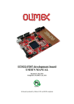
1
OMAP4460 Pandaboard ES System Reference Manual Revision 0.1 September 29, 2011 DOC-21054 OMAP4460 Pandaboard ES System Reference Manual IMPORTANT NOTICE THIS DOCUMENT This work is licensed under the Creative Commons Attribution-Share Alike 3.0 Unported License. To view a copy of this license, visit http://creativecommons.org/licenses/by-sa/3.0/ or send a letter to Creative Commons, 171 Second Street, Suite 300, San Francisco, California, 94105, USA. For more information, see http://creativecommons.org/license/results-one?license_code=by-sa For any questions, concerns, or issues submit them to [email protected] PANDABOARD ES DESIGN These design materials referred to in this document are *NOT SUPPORTED* and DO NOT constitute a reference design. Only “community” support is allowed via resources at: http://Pandaboard.org/content/community/home. THERE IS NO WARRANTY FOR THE DESIGN MATERIALS, TO THE EXTENT PERMITTED BY APPLICABLE LAW. EXCEPT WHEN OTHERWISE STATED IN WRITING THE COPYRIGHT HOLDERS AND/OR OTHER PARTIES PROVIDE THE DESIGN MATERIALS “AS IS” WITHOUT WARRANTY OF ANY KIND, EITHER EXPRESSED OR IMPLIED, INCLUDING, BUT NOT LIMITED TO, THE IMPLIED WARRANTIES OF MERCHANTABILITY AND FITNESS FOR A PARTICULAR PURPOSE. THE ENTIRE RISK AS TO THE QUALITY AND PERFORMANCE OF THE DESIGN MATERIALS IS WITH YOU. SHOULD THE DESIGN MATERIALS PROVE DEFECTIVE, YOU ASSUME THE COST OF ALL NECESSARY SERVICING, REPAIR OR CORRECTION. We mean it; these design materials may be totally unsuitable for any purposes. Pandaboard.org provides the enclosed product(s) under the following conditions: This evaluation board/kit is intended for use for ENGINEERING DEVELOPMENT, DEMONSTRATION, OR EVALUATION PURPOSES ONLY and is not considered by Pandaboard.org to be a finished end-product fit for general consumer use. Persons handling the product(s) must have electronics training and observe good engineering practice standards. As such, the goods being provided are not intended to be complete in terms of required design-, marketing-, and/or manufacturingrelated protective considerations, including product safety and environmental measures typically found in Page 2 of 82 OMAP4460 Pandaboard ES System Reference Manual Revision 0.1 September 29, 2011 DOC-21054 end products that incorporate such semiconductor components or circuit boards. This evaluation board/kit does not fall within the scope of the European Union directives regarding electromagnetic compatibility, restricted substances (RoHS), recycling (WEEE), FCC, CE or UL, and therefore may not meet the technical requirements of these directives or other related directives. Should this evaluation board/kit not meet the specifications indicated in the User’s Guide, the board/kit may be returned within 30 days from the date of delivery for a full refund. THE FOREGOING WARRANTY IS THE EXCLUSIVE WARRANTY MADE BY SELLER TO BUYER AND IS IN LIEU OF ALL OTHER WARRANTIES, EXPRESSED, IMPLIED, OR STATUTORY, INCLUDING ANY WARRANTY OF MERCHANTABILITY OR FITNESS FOR ANY PARTICULAR PURPOSE. The user assumes all responsibility and liability for proper and safe handling of the goods. Further, the user indemnifies Pandaboard.org from all claims arising from the handling or use of the goods. Due to the open construction of the product, it is the user’s responsibility to take any and all appropriate precautions with regard to electrostatic discharge. EXCEPT TO THE EXTENT OF THE INDEMNITY SET FORTH ABOVE, NEITHER PARTY SHALL BE LIABLE TO THE OTHER FOR ANY INDIRECT, SPECIAL, INCIDENTAL, OR CONSEQUENTIAL DAMAGES. Pandaboard.org currently deals with a variety of customers for products, and therefore our arrangement with the user is not exclusive. Pandaboard.org assumes no liability for applications assistance, customer product design, software performance, or infringement of patents or services described herein. Please read the User’s Guide and, specifically, the Warnings and Restrictions notice in the User’s Guide prior to handling the product. This notice contains important safety information about temperatures and voltages. For additional information on Pandaboard.org environmental and/or safety programs, please visit http://Pandaboard.org. No license is granted under any patent right or other intellectual property right of Pandaboard.org covering or relating to any machine, process, or combination in which such Pandaboard.org products or services might be or are used. Page 3 of 82 Revision 0.1 September 29, 2011 DOC-21054 OMAP4460 Pandaboard ES System Reference Manual WARRANTY: The Pandaboard ES is warranted against defects in materials and workmanship for a period of 90 days from purchase. This warranty does not cover any problems occurring as a result of improper use, modifications, exposure to water, excessive voltages, abuse, or accidents. All boards will be returned via standard mail if an issue is found. If no issue is found or express return is needed, the customer will pay all shipping costs. Before returning the board, please visit: http://Pandaboard.org/content/resources/troubleshooting. To return a defective board, please request an RMA at: http://Pandaboard.org/content/return-merchandise-authorization. Page 4 of 82 Revision 0.1 September 29, 2011 DOC-21054 OMAP4460 Pandaboard ES System Reference Manual Preface Read This First About This Manual This manual should be used by software and hardware developers of applications based on the OMAP4460 chipset. This document describes the OMAP4460 Pandaboard ES hardware. This document also gives the user information about the different interfaces on the OMAP4460 Pandaboard ES. Related Documentation OMAP4460 Technical Reference Manual OMAP4460 Pandaboard ES Schematic (750-2170-002-SCH) OMAP4460 Pandaboard ES Gerber Files (720-2170-004) OMAP4460 Pandaboard ES Bill-of-Materials (750-2170-002-EBOM) Page 5 of 82 OMAP4460 Pandaboard ES System Reference Manual Revision 0.1 September 29, 2011 DOC-21054 Revision History Revision History Rev 0.1 Changes Preliminary Release Date 29 Sept. 2011 Page 6 of 82 OMAP4460 Pandaboard ES System Reference Manual Revision 0.1 September 29, 2011 DOC-21054 Contents 1 Introduction...............................................................................................................................................11 OMAP4460 Pandaboard ES Overview .....................................................................................................12 Overview of the OMAP4460 Pandaboard ES Kit Contents......................................................................13 2 OMAP4460 Pandaboard ES Architecture.................................................................................................14 2.1 Overview of the Pandaboard ES Architecture ..........................................................................................14 2.2 System Clock Distribution ........................................................................................................................17 2.3 OMAP4460 Processor...............................................................................................................................17 2.4 TPS62361 External Power Supply (VDD_MPU) .....................................................................................18 2.5 TWL6030 Power Companion IC ..............................................................................................................18 2.5.1 TWL6030 Core SMPS Outputs ...........................................................................................................19 2.5.2 TWL6030 V1V8 SMPS Output...........................................................................................................19 2.5.3 TWL6030 V2V1 SMPS Output...........................................................................................................19 2.5.4 TWL6030 VMEM SMPS Output ........................................................................................................19 2.5.5 TWL6030 V1V29 SMPS Output.........................................................................................................19 2.5.6 TWL6030 LDO Power Resources .......................................................................................................19 2.5.7 TWL6030 Clock Circuitry...................................................................................................................20 2.6 TWL6040 Audio Companion IC ..............................................................................................................21 2.7 SYSBOOT Configuration .........................................................................................................................21 2.8 Miscellaneous Power Circuitry .................................................................................................................26 2.8.1 Input Power Circuitry ..........................................................................................................................26 2.8.2 USB/Ethernet Power Circuitry ............................................................................................................27 2.9 Standard Volatile Memory........................................................................................................................27 2.10 Debug UART Interface .............................................................................................................................28 2.11 SD/MMC Connector .................................................................................................................................28 2.12 HDMI Interface.........................................................................................................................................29 2.13 Display Interface .......................................................................................................................................31 2.13.1 Parallel Display Interface................................................................................................................32 2.13.2 DSI Display Expansion Connector Interface ..................................................................................34 2.14 Bluetooth/WLAN Interfaces .....................................................................................................................36 2.15 Audio Interfaces........................................................................................................................................38 2.16 USB Interfaces ..........................................................................................................................................39 2.16.1 USBOTG Interface .........................................................................................................................39 2.16.2 USBB1 Phy Interface......................................................................................................................40 2.17 Expansion Connectors (J3 & J6)...............................................................................................................41 2.18 Camera Expansion Connector (J17)..........................................................................................................44 2.19 JTAG Connector (J8) ................................................................................................................................45 2.20 LED Indicators..........................................................................................................................................47 2.21 User Interface Features .............................................................................................................................48 1.1 1.2 Page 7 of 82 OMAP4460 Pandaboard ES System Reference Manual Revision 0.1 September 29, 2011 DOC-21054 2.21.1 S1 – Push Button Switch.................................................................................................................48 2.21.2 S2 - Push Button Switch .................................................................................................................48 2.21.3 SW1 – Dip/Slide Switch .................................................................................................................48 2.22 I2C Device Mapping..................................................................................................................................48 2.22.1 OMAP I2C1.....................................................................................................................................48 2.22.2 OMAP I2C2.....................................................................................................................................49 2.22.3 OMAP I2C3.....................................................................................................................................49 2.22.4 OMAP I2C4.....................................................................................................................................49 3 Pandaboard ES S/W Interface...................................................................................................................50 3.1 Readable Board Revision..........................................................................................................................50 3.2 Pandaboard ES Pin Multiplexing ..............................................................................................................50 3.2.1 Panda Base Platform Pin Multiplexing................................................................................................50 3.2.2 Camera Expansion Connector Pin Multiplexing..................................................................................54 3.2.3 Expansion Connector (J3 & J6) Pin Multiplexing ...............................................................................54 3.3 OMAP4460 Pandaboard ES Key Components .........................................................................................56 3.4 OMAP4460 Pandaboard ES Key Component Datasheet URLs ...............................................................58 3.4.1 Connector Datasheets ..........................................................................................................................58 3.4.2 Key Electronic Component Datasheets................................................................................................58 4 Test/Debug Information ............................................................................................................................60 4.1 Pandaboard ES Clock Signal Access ........................................................................................................60 4.1.1 H_FREF_ALTCLK_IN_OMAP Probe Point ......................................................................................60 4.1.2 USBB1_PHY_REFCLK Probe Point ..................................................................................................61 4.1.3 CLK32K_AUD Probe Point ................................................................................................................62 4.2 Pandaboard ES Power Rail Signal Access................................................................................................63 4.2.1 TWL6030 SMPS Output Probe Points ................................................................................................63 4.2.2 VDD_CORE1 Output Probe Point ......................................................................................................63 4.2.3 VCXIO LDO Output Probe Point........................................................................................................64 4.3 Pandaboard ES Interface Signal Access....................................................................................................66 4.3.1 TWL6040 PDM Interface Probe Points...............................................................................................66 4.4 Pandaboard ES Schematic.........................................................................................................................67 4.5 Pandaboard ES Bill of Materials...............................................................................................................82 4.6 Pandaboard ES PCB Design Information .................................................................................................82 Page 8 of 82 OMAP4460 Pandaboard ES System Reference Manual Revision 0.1 September 29, 2011 DOC-21054 Figures Figure 1 – OMAP4460 Pandaboard ES Architectural Block Diagram....................................................... 15 Figure 2 – OMAP4460 Pandaboard ES (Top View) .................................................................................. 16 Figure 3 – SYSBOOT[5:0] Resistor Locations + SYSBOOT3 Switch Location....................................... 23 Figure 4 – Pandaboard ES Input Power Circuitry Block Diagram ............................................................. 26 Figure 5 – Panda UART3/RS-232 Block Diagram..................................................................................... 28 Figure 6 – Panda SDMMC1 Card Cage Block Diagram ............................................................................ 29 Figure 7 – Panda HDMI Interface Block Diagram ..................................................................................... 30 Figure 8 – Panda Display Interface Block Diagram ................................................................................... 31 Figure 9 – Pandaboard ES DSS Output Block Diagram............................................................................. 32 Figure 10 – Panda DSI Display Connector Orientation.............................................................................. 35 Figure 11 – Panda DSI Display Expansion Block Diagram ....................................................................... 36 Figure 12 – Pandaboard ES WLAN/Bluetooth Interface Block Diagram .................................................. 37 Figure 13 – Panda Audio Interface Block Diagram.................................................................................... 39 Figure 14 – Panda USBOTG Interface Block Diagram.............................................................................. 40 Figure 15 – Panda USBB1 Interface Block Diagram ................................................................................. 41 Figure 16 – Expansion Connector PCB Placement/Orientation ................................................................. 42 Figure 17 – 14-pin JTAG Connector (J8) ................................................................................................... 46 Figure 18 – Pandaboard ES LED Locations ............................................................................................... 47 Figure 19 – 38.4 MHz Input Clock Probe Point (h_FREF_ALTCLK_IN_OMAP)................................... 61 Figure 20 – USB Phy Ref Clock In Probe Point (USBB1_PHY_REFCLK).............................................. 61 Figure 21 – 32KHz Audio Clock Probe Point (CLK32K_AUD) ............................................................... 62 Figure 22 – TWL6030 SMPS Output Probe Points .................................................................................... 63 Figure 23 – VDD_CORE1 Output Probe Point .......................................................................................... 64 Figure 24 – TWL6030 VCXIO LDO Output Probe Points ........................................................................ 65 Figure 25 – TWL6040 PDM Interface Probe Points .................................................................................. 66 Page 9 of 82 OMAP4460 Pandaboard ES System Reference Manual Revision 0.1 September 29, 2011 DOC-21054 Tables Table 1: Pandaboard ES Features ............................................................................................................... 12 Table 2: SYSBOOT[5:0] Definitions – Peripheral Preferred Booting ....................................................... 24 Table 3: SYSBOOT[5:0] Definitions – Memory Preferred Booting .......................................................... 25 Table 4: HDMI GPIO Definitions .............................................................................................................. 31 Table 5: DVI-D Display GPIO Definitions ................................................................................................ 33 Table 6: LCD Expansion Connector “A” Pin Definitions (J1) ................................................................... 33 Table 7: LCD Expansion Connector “B” Pin Definitions (J4) ................................................................... 34 Table 8: DSI Display Expansion Connector Pin Definitions (J7)............................................................... 35 Table 9: WLAN/Bluetooth Module GPIO Definitions............................................................................... 38 Table 10: USB Host Port/Ethernet GPIO Definitions................................................................................. 41 Table 11: Expansion Connector “A” Pin Definitions (J3) .......................................................................... 43 Table 12: Expansion Connector “B” Pin Definitions (J6) .......................................................................... 44 Table 13: Camera Expansion Connector Pin Definitions (J17) .................................................................. 45 Table 14: JTAG Connector Pinout (J8) ...................................................................................................... 46 Table 15: OMAP I2C1 Device Addresses................................................................................................... 48 Table 16: OMAP I2C2 Device Addresses................................................................................................... 49 Table 17: OMAP I2C3 Device Addresses................................................................................................... 49 Table 18: OMAP I2C4 Device Addresses................................................................................................... 49 Table 19: Board ID Read Values ................................................................................................................ 50 Table 20: Pandaboard ES OMAP4460 Pin Multiplexing ........................................................................... 54 Table 21: Camera Expansion Connector (J17) Pin Multiplexing Options.................................................. 54 Table 22: Expansion Connector (J3 & J6) Pin Multiplexing Options ........................................................ 55 Table 23: OMAP4460 Pandaboard ES Key H/W Components.................................................................. 57 Page 10 of 82 OMAP4460 Pandaboard ES System Reference Manual Revision 0.1 September 29, 2011 DOC-21054 1 Introduction This document is the System Reference Manual for the Pandaboard ES, a low cost OMAP4460 based board supported through http://Pandaboard.org. This includes system setup and debugging. This document provides detailed information on the overall design and usage of the Pandaboard ES from the System perspective. CAUTION: The Pandaboard ES may reach elevated temperatures. handling the Pandaboard ES while power is applied. Page 11 of 82 Avoid Revision 0.1 September 29, 2011 DOC-21054 OMAP4460 Pandaboard ES System Reference Manual 1.1 OMAP4460 Pandaboard ES Overview Pandaboard ES is an OMAP4460 platform designed to provide access to as many of the powerful features of the OMAP4460 Multimedia Processor as possible, while maintaining a low cost. This will allow the user to develop software to utilize the features of the powerful OMAP4460 processor. In addition, by providing expandability via onboard connectors, the Pandaboard ES supports development of additional capabilities/functionality. See Table 1 for a listing of the Pandaboard ES features. Feature Processor POP Memory PMIC Debug Support PCB Indicators HS USB 2.0 OTG Port HS USB Host Port Audio Connectors SD/MMC Connector OMAP4460 Elpida 8Gb LPDDR2 (EDB8064B1PB-8D-F) TI (TWL6030 Power Management Companion IC) 14-pin JTAG GPIO Pins UART via DB-9 connector LEDs 4.5” x 4.0” (114.3 x 101.6 mm) 8 layers 3 LEDs (two user-controlled, one overvoltage indicator) Mini-AB USB connector, sourced from OMAP USB Transceiver Four USB HS Ports, up to 500mA current out on each, two to onboard connectors, two to expansion connectors 3.5mm, L+R out 3.5mm, Stereo In 6 in 1 SD/MMC/SDIO 4/8 bit support, Dual voltage 1-User defined button Reset Button User Interface SYSBOOT3 switch Video Power Connector Camera Expansion Connectors (not populated) Parallel LCD Expansion Connectors (not populated) DSI LCD Expansion Connector (not populated) Optional user provided plug-in display USB Power DC Power Not included, but supported via camera expansion connector DVI-D or HDMI See Paragraph 2.17 on page 41 See Paragraph 2.13.1 on page 32 See Paragraph 2.13.2 on page 34 Table 1: Pandaboard ES Features Page 12 of 82 Revision 0.1 September 29, 2011 DOC-21054 OMAP4460 Pandaboard ES System Reference Manual 1.2 Overview of the OMAP4460 Pandaboard ES Kit Contents The OMAP4460 Pandaboard ES kit contains the following items: 1 Pandaboard ES Board packing material 1 Shipping Box The following items can be used with the Pandaboard ES, but are NOT included in the kit. USB Cable (mini-AB to Type A) HDMI Cable (Type A) DB-9 Male-to-female cable (straight-through) HDMI-A Male to DVI-D Cable DC wall supply (+5Vdc, 2.0mm center pin diameter/6.5mm outer hole diameter jack) Page 13 of 82 OMAP4460 Pandaboard ES System Reference Manual Revision 0.1 September 29, 2011 DOC-21054 2 OMAP4460 Pandaboard ES Architecture This chapter explains the architecture of the OMAP4460 Pandaboard ES. 2.1 Overview of the Pandaboard ES Architecture Shown in Figure 1 is the Architectural Block Diagram of the OMAP4460 Pandaboard ES. Listed below are the major components used on the Pandaboard ES. OMAP4460 Processor TWL6030 (Phoenix) Power Management Companion Device TWL6040 (Phoenix) Audio Companion Device TPS62361 Switching Power Supply POP Mobile LPDDR2 SDRAM Memory HDMI Connector (Type A) – for OMAP4460 HDMI Transmitter output HDMI Connector (Type A) – for DVI-D output sourced via OMAP4 parallel display output Audio Input & Output Connectors (3.5mm) SD/SDIO/MMC Media Card Cage UART via RS-232 interface via 9-pin D-Sub Connector LS Research Module – 802.11b/g/n, Bluetooth The Platform also includes connectors that can be used for additional functionality and/or expansion purposes. These connectors are not populated on the platform, but can be installed by the user. They are indicated by the blue blocks in Figure 1, and include: Camera Connector (J17) Parallel LCD Expansion Connectors (J1 and J4) Generic Expansion Connectors (J3 and J6) DSI Display Expansion Connector (J7) See Figure 2 on page 16 for a top side view of the Panda Platform. The core components of the Pandaboard ES will be discussed in this section of the document. This would include the OMAP4460 Processor and its POP LPDDR2 memory, the input clock circuitry, the TWL6030 Power Companion IC, and the TWL6040 Audio Companion IC. The functional interfaces will be discussed in later sections of the document. Page 14 of 82 Revision 0.1 September 29, 2011 DOC-21054 OMAP4460 Pandaboard ES System Reference Manual RJ-45 Connector + 2x-USB(A) Host Ports (J9) 32.768 KHz crystal TWL6030 Power CLK32KG Companion IC + External LDOs CLK32KAUDIO CLK32KAO TPS62361 (Core1) Clocks 38.4 MHz USB3320C USB Phy OMAP4460 OMAP4430 Processor TWL6040 Audio PDM, I2C1 DISPC TFP410 I22C2 Companion IC Audio In LAN9514 4 USB Host Ports Ethernet Port DISPC_DAT[23:0], DISPC HSYNC, VSYNC, PCLK, DEN Audio Out 3.5mm Audio Connector (Dual Stacked) (J16) DP/DM USBB1 Input Power Conditioning Circuitry Camera (CSI2-1) DC Input Connector (P3) Camera Board Camera Board Connector (J17) Connector (J17) I C2 DVI-D Connector (P1) Display Display Expansion Expansion Connectors Connectors (J1, J4) (J1, J4) CLK32KAUDIO CLK32KAO SDMMC2, GPMC, McSPI1, I2C4, UART4 HDMI Connector (P2) DSI-2, I2C2, GPIOs HDMI DSI Display Expansion Connector (J7) Hands Free Speaker (R/L) SDMMC Card Cage (J14) Mini-AB USB Connector (J18) SDMMC1 HS-USB (USBA0) POP – LPDDR2 8 Gb/1GB SDMMC2, GPMC, McSPI1, I2C4, UART4 USB Host Ports (x2) Hands Free Speaker (L) GPIOs, VMMC2 JTAG/Trace Connector (J8) UART3 UART2, SDMMC5, McBSP2, I2C4 JTAG, EMU[1:0] CLK32KG LSLS Research Research TiWi-R2 WL1271 (BLE)Module Module (WLAN, (WLAN,BT, BT)GPS) RS-232 Female 9-pin D-Sub (P4) Figure 1 – OMAP4460 Pandaboard ES Architectural Block Diagram . Page 15 of 82 Generic Expansion Connectors (J3, J6) Revision 0.1 September 29, 2011 DOC-21054 OMAP4460 Pandaboard ES System Reference Manual SD/MMC Card Cage (J14) LED “B” LED “A” SYSBOOT3 Switch RS-232 UART3 (P4) DSI Expansion Connector (J7) – Back side of PCB Overvoltage LED Generic Expansion (J3/J6) LCD Expansion (J1/J4) Mini-USB (J18) JTAG (J8) Camera Expansion (J17) OMAP4460 Dual Audio Jack (J16) DC Input Jack (P3) Ethernet + 2X USB Host (J9) OMAP4460 HDMI (P2) OMAP4460 Parallel DSS + DVI (P1) Figure 2 – OMAP4460 Pandaboard ES (Top View) Page 16 of 82 OMAP4460 Pandaboard ES System Reference Manual 2.2 Revision 0.1 September 29, 2011 DOC-21054 System Clock Distribution The OMAP4460 Pandaboard ES implements a 38.4 MHz 1.8V CMOS square-wave oscillator that directly drives the FREF_SLICER_IN input (ball AG8) of the OMAP4460 processor and the MCLK input to the TWL6040 Audio Companion IC. This clock is used as an input to the PLLs within the OMAP4460 processor so that it can generate all the internal clock frequencies required for system operation. 2.3 OMAP4460 Processor The heart of Pandaboard ES is the OMAP4460 processor. The OMAP4460 high-performance multimedia application device is based on enhanced OMAP™ architecture and uses 45-nm technology. For more information, refer to the OMAP4460 Technical Reference Manual (TRM).The architecture is designed to provide best-in-class video, image, and graphics processing sufficient to various applications. The device supports the following functions: Streaming video up to full high definition (HD) (1920 × 1080 p, 30 fps) 2-dimensional (2D)/3-dimensional (3D) mobile gaming Video conferencing High-resolution still image (up to 16 Mp) The device supports high-level operating systems (OSs) such as: Windows™ CE, WinMobile™ Symbian OS™ Linux® Palm OS™ The device is composed of the following subsystems: Cortex™-A9 microprocessor unit (MPU) subsystem, including two ARM® Cortex-A9 cores capable of operation at 1.2GHz Digital signal processor (DSP) subsystem Image and video accelerator high-definition (IVA-HD) subsystem Cortex™-M3 MPU subsystem, including two ARM Cortex-M3 microprocessors Display subsystem Audio back-end (ABE) subsystem Imaging subsystem (ISS), consisting of image signal processor (ISP) and still image coprocessor (SIMCOP) block 2D/3D graphic accelerator (SGX) subsystem Emulation (EMU) subsystem The device includes state-of-art power-management techniques required for high-performance mobile products. Comprehensive power management is integrated into the device. The device also integrates: On-chip memory External memory interfaces Memory management Level 3 (L3) and level 4 (L4) interconnects Page 17 of 82 OMAP4460 Pandaboard ES System Reference Manual 2.4 Revision 0.1 September 29, 2011 DOC-21054 System and connecting peripherals TPS62361 External Power Supply (VDD_MPU) The VDD_MPU balls on the OMAP4460 processor that power the ARM cores are supplied by an external switch mode supply at U25. This device is a Texas Instruments TPS62361 switch mode supply that is controllable via the smart reflex I2C interface of the OMAP4460 processor. Additionally, the VSEL0 ball of the converter is controlled by an OMAP GPIO (GPIO_WK7). This part may be found on sheet 2 of the schematics. 2.5 TWL6030 Power Companion IC The TWL6030 device is a small (7 x 7 mm, 0.4mm pitch) 256 ball FBGA that provides many functions used on the Platform. Shown below is a feature list of the major functions/interfaces provided by the TWL6030 device that are utilized on the Panda platform. This list below doesn’t include all device functionality, just that which is used on the Pandaboard ES. A power management system (FSM) 1 HS-I2C interface (≤ 2.4Mbits/s) for all Phoenix Power IC GP control commands (CTL-I2C) 1 HS-I2C interface (≤ 2.4Mbits/s) for all Smart-Reflex Class 3 control commands (SR-I2C) MMC card detection mechanism A 24MHz RC oscillator A 32kHz RC oscillator for a fast device start-up A high-performance crystal oscillator, for 32.768kHz external crystal A Real Time Clock (RTC) resource Power supply resources: o 11 Low Drop Out (LDO) regulators 1 for internal purposes only (VRTC) 1 for internal and platform needs (VANA) 9 for platform needs (VAUX1, VAUX2, VAUX3, VCXIO, VDAC, VMMC, VPP, VUSB, VUSIM) o 7 buck SMPS with: DVS capability Smart-Reflex Class 3 compatible (VCORE1, VCORE2, VCORE3) 1 for I/O supply (V1V8), with specific PWMFORCE input control 1 for LDOs pre-regulation (V2V1) and Phoenix Audio features 1 for memory supply (VMEM) 1 for external modem, RF transceiver or I/Os (V1V29) 3 general-purpose enables for possible platform upgrades (REGEN1, REGEN2, SYSEN) Page 18 of 82 OMAP4460 Pandaboard ES System Reference Manual Revision 0.1 September 29, 2011 DOC-21054 2.5.1 TWL6030 Core SMPS Outputs The TWL6030 implements three Switch Mode Power Supplies (SMPS) that source two of the three main core voltage rails for the OMAP4460 processor. The default voltage of all of these supplies is 0.95V, and each should be adjusted as required by S/W for the desired processor OPP. VCORE1 is a 1200mA SMPS that is used to power the VDD_CORE balls on the OMAP4460 processor (net name VDD_VCORE3, (34 balls total) and the VDDA_DLLn_LPDDR21 and VDDA_DLLn_ LPDDR22 balls, where n=0/1 (4 balls total). VCORE2 is a 600mA SMPS that is used to power the VDD_IVA_AUDIO balls on the processor (net name VDD_VCORE2, 10 balls total). VCORE3 is a 600mA SMPS that is not used on the OMAP4460 Pandaboard ES. 2.5.2 TWL6030 V1V8 SMPS Output The TWL6030 V1V8 SMPS provides the I/O voltage for the Pandaboard ES (net name VIO_1v8). This is a 1200mA SMPS that provides a 1.8V output that is used to power many balls on the OMAP4460 processor that set the I/O voltage for the device. It also sources onboard peripherals that require an operating voltage referenced to processor I/Os. 2.5.3 TWL6030 V2V1 SMPS Output The TWL6030 V2V1 SMPS output is used by the TWL6040 Audio Companion IC as an input for some of its internal power supplies (specifically the high side and low side LDOs and the negative charge pump). It is also connected to the TWL6030 as the input voltage to the VCXIO and VDAC LDOs (net name VDD_2V1). It is a 600mA SMPS with a default output value of 2.10V. 2.5.4 TWL6030 VMEM SMPS Output The TWL6030 VMEM SMPS is not used on the OMAP4460 Pandaboard ES. The LPDDR2 power balls on the OMAP4460 that were previously connected to this rail for the OMAP4430 are connected to the V1V29 SMPS. 2.5.5 TWL6030 V1V29 SMPS Output The TWL6030 V1V29 output is a 600mA SMPS used to provide the operating voltage for the VDD2 LPDDR2 balls on the OMAP4460 processor (net name VDD_VMEM). These OMAP balls are feedthroughs to the top POP footprint on the OMAP package, where they directly connect to the LPDDR2 VDD2 balls. This SMPS is a 600mA max capacity rail. The Micron LPDDR2 device used is an S4B type device, so VDD2 is required to be 1.2V. This is set in the TWL6030 companion chip by connecting the BOOT1 input to VRTC, which causes V1V29 to be set to a default of 1.225V. 2.5.6 TWL6030 LDO Power Resources The VAUX2 LDO is a programmable LDO that is only connected to pin 1 of the LCD Expansion Connector J4. Its possible output voltage settings include 1.2V, 1.8V, 2.5V, 2.75V, and 2.8V, and its maximum output current is 200mA. The voltage to be programmed will be dependent on the board plugged into the LCD Expansion connectors, but will most likely be 2.8V. Page 19 of 82 OMAP4460 Pandaboard ES System Reference Manual Revision 0.1 September 29, 2011 DOC-21054 The VAUX2 LDO is a programmable LDO that is only connected to pin 1 of the LCD Expansion Connector J4. Its possible output voltage settings include 1.2V, 1.8V, 2.5V, 2.75V, and 2.8V, and its maximum output current is 200mA. The voltage to be programmed will be dependent on the board plugged into the LCD Expansion connectors, but will most likely be 2.8V. The VAUX3 LDO is a programmable LDO that is only connected to pin 30 of the Camera Expansion Connector, J17. Its possible output voltage settings include 1.0V, 1.2V, 1.3V, 1.8V, 2.5V, 2.8V, 3.0V, and its maximum output current is 200mA. The output voltage to be utilized would depend on the implementation of the camera module. The VCXIO LDO is a fixed 1.8V, 200mA LDO that provides a 1.8V input to certain noise sensitive OMAP4460 balls. The balls powered by this LDO include the VDDA_CSI2 balls (V28 and W28), the VDDA_DPLL balls (G13, P9 and Y16), and on this revision of the Pandaboard ES, the VDDS_DV_BANK7 ball (M28). This LDO also provides power for the onboard 38.4 MHz oscillator. The VDAC LDO is a fixed 1.8V, 50mA LDO that provides a 1.8V input to certain noise sensitive OMAP4460 balls. The balls powered by this LDO include the VDDA_HDMI_VDAC balls (A11 and G12). The VMMC LDO is a programmable LDO that provides the voltage to the VDDS_MMC1 balls on the OMAP processor (pins G7 and H7) as well as the SDMMC cardcage. This LDO is off when the board is powered on, but is turned on and set to 1.8V or 3.0V depending on card capabilities detected. The VRTC LDO is an adjustable LDO that provides internal voltages to the TWL6030 device. Its possible output voltage settings are 1.8V and 2.5V and its maximum output current is 25mA. In normal operation, it should always be set to 1.8V. The VUSB LDO is a fixed 3.3V, 35mA LDO that provides voltage to the OMAP4460 that it uses for its internal USB transceiver. The only ball powered by this LDO is the VDDA_USBA0OTG_3P3V ball (ball A5). The VPP LDO is adjustable LDO that powers the VPP_CUST and VPP_STD balls on OMAP (balls J8 and Y22). This LDO is only needed for eFuse operations and can be left disabled for normal Pandaboard ES operation. 2.5.7 TWL6030 Clock Circuitry The TWL6030 has an 32.768 KHz crystal connected across its OSC32KIN and OSC32KOUT balls. This crystal is used by the TWL6030 to generate three output 32.768 KHz, 1.8V square wave clock outputs. These outputs are: CLK32KAO: always on clock connected to the SYS32K input of the OMAP4460 processor. CLK32KAUDIO: clock connected to the CLK32K input of the TWL6040 Audio Companion IC. Page 20 of 82 OMAP4460 Pandaboard ES System Reference Manual Revision 0.1 September 29, 2011 DOC-21054 CLK32KG: a gated 32.768 clock connected to the SLOW_CLK input of the LS Research module. This clock will be off by default at reset, and must be enabled by software. 2.6 TWL6040 Audio Companion IC The TWL6040 device is a small (6 x 6 mm, 0.5mm pitch) 120 ball PBGA that provides many functions, primarily audio, used on the Platform. Shown below is a feature list of the major functions/interfaces provided by the TWL6040 device. A audio management system o PDM Interface for Audio and control o Analog Microphone Interface o Headset – speaker (32 ohm) and microphone o Earpiece Output o Aux Output o Hands-free 8 ohm driver o Dual Vibrator Misc Control o GPO o I2C (high speed) o Power on/off Power o Internal LDOs o Internal negative charge pump 2.7 SYSBOOT Configuration The OMAP4460 Processor has eight SYSBOOT inputs. These inputs are sampled after a board reset, and determine the booting and operating mode of the OMAP4460 Processor. The upper two inputs (SYSBOOT[7:6]) control the clocking modes of the part (i.e. enabling/disabling the internal oscillator to allow using a crystal input or oscillator). They are currently set to “11” and should not be changed. The lower six inputs, SYSBOOT[5:0] determine the type and order of memory or peripheral booting. SYSBOOT[5] determines whether memory or peripheral booting is preferred. The SYSBOOT definitions may be found in the OMAP4460 TRM, but are included here for convenience. See Table 2 on page 24 for the SYSBOOT definitions for peripheral preferred booting, and Table 3 on page 25 for memory preferred booting SYSBOOT definitions. The shaded row(s) in Table 2 are the default configuration of the Pandaboard ES, depending on the setting of SW1. If it is desired to change the SYSBOOT configuration, resistors may be added or removed from the SYSBOOT[5:0] lines (except for SYSBOOT3, which may be changed by changing the position of switch SW1). The SYSBOOT[5:0] lines have weak internal pull-down resistors inside the OMAP4460, so removing the onboard resistor will result in the line being sampled as a ‘0’ at reset, and installing a 3.3K Page 21 of 82 OMAP4460 Pandaboard ES System Reference Manual Revision 0.1 September 29, 2011 DOC-21054 or lower value resistor will result in the line being sampled as a ‘1’ at reset. See Figure 3 on page 23 for the location of the resistors on SYSBOOT[5:0]. These resistors are connected to OMAP4460 as follows: SYSBOOT0: R123 SYSBOOT1: R138 SYSBOOT2: R128 SYSBOOT3: N/A (controlled by switch SW1) SYSBOOT4: R137 SYSBOOT5: R139 NOTE: Do not use pull-up resistance values higher than 3.3Kohm on the SYSBOOT lines. This would create a voltage divider with the internal OMAP pulldown, potentially causing an invalid value to be internally latched for SYSBOOT. Page 22 of 82 OMAP4460 Pandaboard ES System Reference Manual Revision 0.1 September 29, 2011 DOC-21054 Figure 3 – SYSBOOT[5:0] Resistor Locations + SYSBOOT3 Switch Location Page 23 of 82 Revision 0.1 September 29, 2011 DOC-21054 OMAP4460 Pandaboard ES System Reference Manual Booting Devices Order 2nd 3rd MMC2(1) XIP XIPWAIT NAND EMIF MMC1 OneNAND OneNAND MMC2(1) MMC2(1) XIP XIPWAIT NAND EMIF MMC1 OneNAND MMC2(1) XIP XIPWAIT NAND EMIF MMC1 OneNAND UART MMC1 UART MMC1 UART MMC2(2) UART MMC1 MMC2(2) UART MMC1 MMC2(2) Reserved Reserved Fast XIP booting. Wait monitoring off USB SYSBOOT[5:0] (1) 1st USB USB USB USB USB USB USB USB UART UART UART UART UART UART UART USB-ULPI USB-ULPI USB-ULPI USB-ULPI USB-ULPI USB-ULPI USB-ULPI USB USB USB-ULPI USB UART USB USB 000000 000001 000010 000011 000100 000101 000110 000111 001000 001001 001010 001011 001100 001101 001110 001111 010000 010001 010010 010011 010100 010101 010110 010111 011000 011001 011010 011011 011100 011101 011110 011111(1) 4th MMC2(1) XIP Only on GP devices Table 2: SYSBOOT[5:0] Definitions – Peripheral Preferred Booting Page 24 of 82 NAND UART Revision 0.1 September 29, 2011 DOC-21054 OMAP4460 Pandaboard ES System Reference Manual SYSBOOT[5:0] (1) 100000 100001 100010 100011 100100 100101 100110 100111 101000 101001 101010 101011 101100 101101 101110 101111 110000 110001 110010 110011 110100 110101 110110 110111 111000 111001 111010 111011 111100 111101 111110 111111(1) Booting Devices Order 2nd 3rd USB USB USB USB USB USB USB MMC2(1) USB UART UART UART UART UART UART UART USB-ULPI USB-ULPI USB-ULPI USB-ULPI USB-ULPI USB-ULPI USB-ULPI USB UART USB UART USB-ULPI UART USB UART UART USB UART USB Reserved Reserved Fast XIP booting. Wait monitoring off USB 1st MMC2(1) XIP XIPWAIT NAND EMIF MMC1 OneNAND OneNAND MMC2(1) XIP XIPWAIT NAND EMIF MMC1 OneNAND MMC2(1) XIP XIPWAIT NAND EMIF MMC1 OneNAND MMC2(1) XIP MMC2(2) NAND MMC2(2) MMC1 MMC2(2) Only on GP devices Table 3: SYSBOOT[5:0] Definitions – Memory Preferred Booting Page 25 of 82 4th MMC1 MMC1 MMC1 UART OMAP4460 Pandaboard ES System Reference Manual 2.8 Miscellaneous Power Circuitry 2.8.1 Input Power Circuitry Revision 0.1 September 29, 2011 DOC-21054 The input power circuitry may be found on sheet 2 of the board schematic. A block diagram of this circuitry is shown in Figure 4 below. The Pandaboard ES may be run either with or without a DC wall supply plugged into the input power jack at P3. Without an external power supply plugged in, the 5Vdc input power is supplied from the mini-AB USBOTG connector at J18. This supply is only capable of providing 500mA of output current (1A if operating via a USB cable with a “Y” connection to the host), so board operations will be limited in this mode (e.g. operations could be limited, depending on current requirements). The path of current flow in this mode is designated below by the red arrow. The 5V from VBUS will be routed through the switch at U21, to the TPS54320 switching power supply at U22, which provides a 3.7V “battery” voltage for the TWL6030 and TWL6040 Companion ICs. Figure 4 – Pandaboard ES Input Power Circuitry Block Diagram Page 26 of 82 OMAP4460 Pandaboard ES System Reference Manual Revision 0.1 September 29, 2011 DOC-21054 With an external power supply plugged in, the 5Vdc input power is supplied from the input DC jack at P3. The current capability in this mode is only limited by the particular DC supply being used. The path of current flow in this mode is designated below by the blue arrows. The switch at U21 will be disabled by the insertion of the DC input jack in this mode, and the regulated 5Vdc from the wall supply will be connected to the input of the TPS54320 switching power supply at U22, which provides a 3.7V “battery” voltage for the TWL6030 and TWL6040 Companion ICs. CAUTION: only use a 5Vdc regulated power supply to power the Pandaboard ES. Connecting a supply with an output higher than +5Vdc could cause possible board damage. The supervisor IC at U19 has the DC input power tied to its VDD pin through a voltage divider. When the voltage at the VDD input of this IC exceeds 1.40V (i.e. DCIN_JACK > 5.64V), the reset output of the supervisor is negated. This will enable the two FETs at T1A and T1B, which will illuminate the red overvoltage indicator, and disable the load switch at U16, which removes input power to the onboard circuitry. The load switch at U14 that provides 5V USB Host power is enabled and disabled manually by writing GPIO_1 to a ‘1’, or a ‘0’, respectively. This load switch powers up disabled. 2.8.2 USB/Ethernet Power Circuitry There is a fixed 3.3V LDO (U11) that provides power for the LAN9514 Ethernet/USB Hub device. This device is a Texas Instruments TPS73633DBVR device which can provide up to 400mA of output current. This device may be controlled via S/W by writing OMAP4460 GPIO_1. Writing this GPIO high will enable this LDO, while writing it low will disable it (see Table 10 on page 41). This device is shown on sheet 11 of the schematic. 2.9 Standard Volatile Memory The OMAP4460 processor supports two LPDDR2 channels, accessible only via a POP memory device soldered on the 216-ball, 12x12 mm footprint on top of the OMAP4460 processor. Each channel supports up to two chip-selects, so up to four LPDDR2 memory dies are supported. The two stacked memory packages are directly connected to the two LPDDR2 EMIF4D interfaces of the OMAP4460 die. The base address for the LPDDR2 is 0x8000 0000. An 8Gb/1GB POP LPDDR2 DRAM device (Elpida P/N EDB8064B1PB-8D-F) is provided on the Pandaboard ES. The memory device has four dies, with each die being a separate 2Gb LPDDR2. Page 27 of 82 Revision 0.1 September 29, 2011 DOC-21054 OMAP4460 Pandaboard ES System Reference Manual 2.10 Debug UART Interface A single RS-232 port is provided on the Pandaboard ES via 9-pin D-sub female connector at location P4. It provides access to the UART3 interface of the OMAP4460. See Figure 5 for the implementation of the RS232 port. The TXS0104EZXUR device at U20 is a voltage translator that translates between the 1.8V logic levels required by the OMAP4460 processor to the 3.3V logic levels required by the SN75C3232EDR. The SN75C3232EDR @ U23 is an RS-232 transceiver that converts the 3.3V logic signals to/from the voltage translator to the RS-232 signal levels required (-5V to +5V). The UART port at P4 can be accessed by using Teraterm or other terminal emulation program. To use this UART interface, the serial port settings should be applied as follows: BAUD RATE: 115200 DATA: 8 bit PARITY: none STOP: 1bit FLOW CONTROL: none This port requires the use of a 9-pin D-sub Male to Female cable. Figure 5 – Panda UART3/RS-232 Block Diagram 2.11 SD/MMC Connector The OMAP4460 Pandaboard ES supports removable memory storage via onboard SD/MMC card cage. It is an eight-bit card cage that supports 1.8V or 3.0V cards. Card detect functionality is supported via the TWL6030 power companion IC. See Figure 6 for a block diagram of the interface signaling to the card cage. The resistors shown in Figure 6 below are 33 ohm series termination resistors. Page 28 of 82 Revision 0.1 September 29, 2011 DOC-21054 OMAP4460 Pandaboard ES System Reference Manual OMAP4460 6-in-1 Cardcage SDMMC1_CLK/GPIO_100 O SDMMC1_CMD/GPIO_101 IO SDMMC1_DAT0/GPIO_102 IO SDMMC1_DAT1/GPIO_103 IO SDMMC1_DAT2/GPIO_104 IO SDMMC1_DAT3/GPIO_105 IO SDMMC1_DAT4/GPIO_106 IO SDMMC1_DAT5/GPIO_107 IO SDMMC1_DAT6/GPIO_108 IO SDMMC1_DAT7/GPIO_109 IO VDDS_SDMMC1 (G7/H7) R124 I R126 R131 R127 R125 R129 R119 R120 R116 R115 I VIO_V1v8 R149 CLK IO CMD IO DAT0 IO DAT1 IO DAT2 IO DAT3 IO DAT4 IO DAT5 IO DAT6 IO DAT7 IO VCC (4, 19) O CD TWL6030 I MMC O VMMC Figure 6 – Panda SDMMC1 Card Cage Block Diagram 2.12 HDMI Interface The OMAP4460 Pandaboard ES provides a High-Definition Multimedia Interface (HDMI) via an industry-standard Type A connector at location P2. The interface is provided using the internal HDMI module provided by the OMAP4460. See Figure 7 for a block diagram of the Pandaboard ES HDMI circuitry. This interface includes a Texas Instruments TPD12S015A HDMI Port Protection/Interface device. The high-speed differential clock and data lines are connected straight from OMAP to the ESD protection device, to the connector, so that any ESD event experienced at the connector will be absorbed before damaging the OMAP4460 device I/Os. Page 29 of 82 Revision 0.1 September 29, 2011 DOC-21054 OMAP4460 Pandaboard ES System Reference Manual TPD12S015A D2- D2+ SDA_B SCL_B CEC_B HPD_B 5VOUT E E IO O IO I P D1- D1+ E E D0- D0+ E SDA_A IO E SCL_A I CLK- CEC_A IO CLK+ HPD_A O E CT_CP_HPD I E LS_OE I P (U5) R37 R36 OMAP4460 DNI DNI HDMI Connector Type A (P2) GPIO_41 O GPIO_60 O I 5Vdc HDMI_HPD/GPIO_63 I O HPLG HDMI_CEC/GPIO_64 IO IO CEC HDMI_DDC_SCL/GPIO_65 O I SCL HDMI_DDC_SDA/GPIO_66 IO IO SDA HDMI_CLOCKX O I CLK- HDMI_CLOCKY O IO CLK+ HDMI_DATA0X O IO DAT0- HDMI_DATA0Y O IO DAT0+ HDMI_DATA1X O IO DAT1- HDMI_DATA1Y O IO DAT1+ HDMI_DATA2X O IO DAT2- HDMI_DATA2Y O IO DAT2+ Figure 7 – Panda HDMI Interface Block Diagram In addition to providing ESD protection on the signals coming from the connector, this device performs voltage translation on the control signals in the HDMI interface (SCL, SDA, CEC, and HPD) from the 1.8V levels of the OMAP4460 to the 5V levels required by a TV set. It also implements a DC/DC boost converter that operates from the “battery” voltage, VBAT, and outputs a 5Vdc output that is capable of sourcing up to 55mA of current. See Table 4 for the GPIOs used on the HDMI interface and a description of their function. The direction column in this table indicates whether this device is an output from OMAP (O) or an input to OMAP (I). Page 30 of 82 Revision 0.1 September 29, 2011 DOC-21054 OMAP4460 Pandaboard ES System Reference Manual GPIO Dir Signal Name GPIO_41 O HDMI_LS_OE GPIO_60 O HDMI_CT_CP_HPD Description TPD12S015A Level Shifter and internal LDO Enable 1 = Enabled, 0 = Disabled TPD12S015A DC/DC Converter and Hot-Plug Detect Enable 1 = Enabled, 0 = Disabled Table 4: HDMI GPIO Definitions 2.13 Display Interface The Pandaboard ES provides two possible options for the usage of the OMAP4460 parallel display signals. The first option is to use the onboard TFP410 DVI transmitter, whose output feeds an onboard DVI-D connector. The second option is to use a Display Board plugged into a pair of 20-pin LCD expansion connectors (J1 and J4). Both of these possible options are discussed in the following paragraphs. Additionally, a third display option has been added to the OMAP4460 Pandaboard ES. This option is using a DSI Display Board plugged into connector J7 on the back side of the PCB. See Figure 8 for a diagram of the Pandaboard ES Display Interface options. Figure 8 – Panda Display Interface Block Diagram Page 31 of 82 Revision 0.1 September 29, 2011 DOC-21054 OMAP4460 Pandaboard ES System Reference Manual 2.13.1 Parallel Display Interface See Figure 9 for a detailed block diagram of the OMAP4460 Pandaboard ES parallel display interface. (NOTE: J1/J4 are pin-compatible with the OMAP3530 BeagleBoard, so display boards designed for it may be used with the OMAP4460 Pandaboard ES). OMAP4460 O DISPC2_DATA1/GPIO_190 O DISPC2_DATA2/GPIO_28 O DISPC2_DATA3/GPIO_27 O DISPC2_DATA4/GPIO_26 O DISPC2_DATA5/GPIO_25 O DISPC2_DATA6/GPIO_24 O DISPC2_DATA7/GPIO_23 O DISPC2_DATA8/GPIO_22 O DISPC2_DATA9/GPIO_15 O DISPC2_DATA10/GPIO_14 O DISPC2_DATA11/GPIO_168 O DISPC2_DATA12/GPIO_167 O DISPC2_DATA13/GPIO_166 O DISPC2_DATA14/GPIO_165 O DISPC2_DATA15/GPIO_164 O DISPC2_DATA16/GPIO_16 O DISPC2_DATA17/GPIO_17 O DISPC2_DATA18/GPIO_163 O DISPC2_DATA19/GPIO_162 O DISPC2_DATA20/GPIO_161 O DISPC2_DATA21/GPIO_160 O DISPC2_DATA22/GPIO_159 O DISPC2_DATA23/GPIO_158 O Parallel Display Expansion Connectors (J1 & J4) Series Terminations DISPC2_DATA0/GPIO_191 (U1) I DATA[23:0] I IDCK+ I VSYNC DISPC2_PCLK/GPIO_19 O I HSYNC I DE DISPC2_VSYNC/GPIO_20 O DISPC2_HSYNC/GPIO_18 O DISPC2_DE/GPIO_21 O GPIO_0 O I PDn GPIO_122 I O MSEN VIO_1V8 DVI-D Connector (P1) TFP410PAP TXC+ O I CLK+ TXC- O I CLK- TXD0+ O I DAT0+ TXD0- O I DAT0- TXD1+ O I DAT1+ TXD1- O I DAT1- TXD2+ O I DAT2+ TXD2- O I DAT2- R23 Voltage Translator (U3) I2C3_SCL/GPIO_130 O I SCL_L SCL_H O I SCL I2C3_SDA/GPIO_131 IO IO SDA_L SCL_L IO IO SDA 1.8v/5.0v Figure 9 – Pandaboard ES DSS Output Block Diagram Page 32 of 82 Revision 0.1 September 29, 2011 DOC-21054 OMAP4460 Pandaboard ES System Reference Manual See Table 5 for the GPIOs used on the Parallel display interface and a description of their function. This table does not include the 28 parallel display signals (DATA[23:0], PCLK, VSYNC, HSYNC, and DE). NOTE: no configuration changes are required to switch between usage of the onboard DVI connector or an external display plugged into the display expansion connectors. GPIO Signal Name GPIO_0 H_GPIO_0/ TFP410_NPD GPIO_122 DVI_MSEN Description TFP410 Device Power down (note: this GPIO goes through a voltage translator to meet the 3.3V I/O requirement of the TFP410 on this pin) 1 = Normal Operation, 0 = Power Down TFP410 Monitor Sense 0 = Powered on receiver sensed at the differential outputs 1 = No powered on receiver detected. (note: this output from the TFP410 is open-drain and has a pull-up to 1.8V, so it is connected directly to OMAP) Table 5: DVI-D Display GPIO Definitions See Table 6 and Table 7 for the pinout of the display expansion connectors. Pin# 1 2 3 4 5 6 7 8 9 10 11 12 13 14 15 16 17 18 19 20 Signal DCIN_JACK DCIN_JACK h_DSS_DAT1 h_DSS_DAT0 h_DSS_DAT3 h_DSS_DAT2 h_DSS_DAT5 h_DSS_DAT4 h_DSS_DAT12 h_DSS_DAT10 h_DSS_DAT23 h_DSS_DAT14 h_DSS_DAT19 h_DSS_DAT22 H_I2C2_SDA h_DSS_DAT11 h_DSS_VSYNC H_DPM_EMU2 GND GND I/O PWR PWR I I I I I I I I I I I I I/O I I I PWR PWR Description DC rail from the Main DC supply DC rail from the Main DC supply LCD Pixel Data bit 1 LCD Pixel Data bit 0 LCD Pixel Data bit 3 LCD Pixel Data bit 2 LCD Pixel Data bit 5 LCD Pixel Data bit 4 LCD Pixel Data bit 12 LCD Pixel Data bit 10 LCD Pixel Data bit 23 LCD Pixel Data bit 14 LCD Pixel Data bit 19 LCD Pixel Data bit 22 I2C2 Serial Data LCD Pixel Data bit 11 LCD Vertical Sync Signal DPM_EMU2/GPIO_13 Ground bus Ground bus Table 6: LCD Expansion Connector “A” Pin Definitions (J1) Page 33 of 82 OMAP4460 Pandaboard ES System Reference Manual Pin# 1 2 3 4 5 6 7 8 9 10 11 12 13 14 15 16 17 18 19 20 Signal VDD_VAUX2 VIO_1V8 h_DSS_DAT20 h_DSS_DAT21 h_DSS_DAT17 h_DSS_DAT18 h_DSS_DAT15 h_DSS_DAT16 h_DSS_DAT7 h_DSS_DAT13 h_DSS_DAT8 NUSB_PWR h_DSS_DAT9 H_I2C2_SCL h_DSS_DAT6 h_DSS_PCLK h_DSS_DEN h_DSS_HSYNC GND GND I/O PWR PWR I I I I I I I I I O I I I I I I PWR PWR Revision 0.1 September 29, 2011 DOC-21054 Description Power rail (adjustable from 1.2V to 2.8V) 1.8V system I/O voltage LCD Pixel Data bit 20 LCD Pixel Data bit 21 LCD Pixel Data bit 17 LCD Pixel Data bit 18 LCD Pixel Data bit 15 LCD Pixel Data bit 16 LCD Pixel Data bit 7 LCD Pixel Data bit 13 LCD Pixel Data bit 8 Input Power Enable LCD Pixel Data bit 9 I2C2 Serial Clock LCD Pixel Data bit 6 LCD Pixel Clock LCD Data Enable LCD Horizontal Sync Ground bus Ground bus Table 7: LCD Expansion Connector “B” Pin Definitions (J4) 2.13.2 DSI Display Expansion Connector Interface A third display option for the Pandaboard ES is to plug an external display module into the DSI display expansion connector J7. This connector is a 40-pin, 0.8mm pitch connector (Hirose P/N FX6A-40P-0.8SV91), and is mounted on the back side of the Pandaboard ES PCB. See Figure 10 below for the orientation/pin numbering of this connector as viewed from the back side of the PCB. A block diagram of the Pandaboard ES Display Expansion interface is shown in Figure 11 on page 36. Page 34 of 82 Revision 0.1 September 29, 2011 DOC-21054 OMAP4460 Pandaboard ES System Reference Manual 40 2 39 1 Figure 10 – Panda DSI Display Connector Orientation See Table 8 for the pinout of J7 and a description of the signals on the connector. Any pin not shown in Table 8 is not connected. J7 Pin # OMAP Ball # Signal Name 1,3 2,4 ----- VIO_1V8 VBAT Multiple --- DGND 10 11 13 17 18 19 20 23 24 25 29 30 31 34 35 37 38 --P3 P4 N3 C26 N4 D26 M3 D21 M4 L3 AG24 L4 B24 K3 K4 A24 PHO_PWM1 DSI1_DX0 DSI1_DY0 DSI1_DX1 h_I2C2_SCL DSI1_DY1 h_I2C2_SDA DSI1_DX2 TSC_nINT DSI1_DY2 DSI1_DX3 h_DMTIMER11_PWM DSI1_DY3 h_GPIO_102 DSI1_DX4 DSI1_DY4 H_DSI1_TE0 Signal Description VIO from TWL6030 Battery input voltage Signal Ground (connected on pins 9, 12, 15, 21, 22, 27, 32, 33, 39, and 40) PWM1 output of TWL6030 device DSI Signal Lane 0 Data X DSI Signal Lane 0 Data Y DSI Signal Lane 1 Data X I2C Clock In DSI Signal Lane 1 Data Y I2C Data I/O DSI Signal Lane 2 Data X Touchscreen Interrupt Out (GPIO_52) DSI Signal Lane 2 Data Y DSI Signal Lane 3 Data X Display PWM (GPIO_121) DSI Signal Lane 3 Data Y LCD Reset (GPIO_102) DSI Signal Lane 4 Data X DSI Signal Lane 4 Data Y Display Tearing Effect (GPIO_101) Table 8: DSI Display Expansion Connector Pin Definitions (J7) Page 35 of 82 Revision 0.1 September 29, 2011 DOC-21054 OMAP4460 Pandaboard ES System Reference Manual DSI Display Expansion (J7) OMAP4460 DSI1_DX0 O I DSI1_DY0 O I DSI_D0- DSI1_DX1 O I DSI_D1+ DSI1_DY1 O I DSI_D1- DSI1_DX2 O I DSI_D2+ DSI1_DY2 O I DSI_D2- DSI1_DX3 O I DSI_D3+ DSI1_DY3 O I DSI_D3- DSI1_DX4 O I DSI_D4+ DSI1_DY4 O I DSI_D4- DSI1_TE0/GPIO_101 O I Tearing Effect GPIO_102 O I LCD_RST GPIO_52 O I TSC_nINT DMTIMER11_PWM/GPIO_121 O I PWM_IN (A) DSI_D0+ I2C2_SCL/GPIO_128 O I SCL I2C2_SDA/GPIO_129 IO IO SDA VBAT PWM1 O VIO_1V8 P I PWM_IN (B) TWL6030 Figure 11 – Panda DSI Display Expansion Block Diagram 2.14 Bluetooth/WLAN Interfaces The Pandaboard ES provides a module (LS Research Inc. P/N TiWi-BLE) that provides a Bluetooth interface, and a 2.4 GHz 802.11b/g/n interface. This module may be found on sheet 14 of the schematics (reference designator U3). It uses Texas Instruments’ WiLinkTM 6.0 solution. Information for this module may be found at: http://www.lsr.com. See Figure 12 for a diagram of the Pandaboard ES connectivity to this module. See Table 9 on page 38 for a description of the GPIOs used to interface to the module and their function. Page 36 of 82 Revision 0.1 September 29, 2011 DOC-21054 OMAP4460 Pandaboard ES System Reference Manual The OMAP4460 interfaces are connected to the LS Research WiLinkTM module as follows: SDMMC5: WLAN SDIO interface UART2: Bluetooth Host Control Interface McBSP1: Audio Digital PCM Path OMAP4460 TiWi Module R15* Antenna Connector R14 Chip Antenna (2.4 GHz) (U3) SDMMC5_CLK/GPIO_145 O I SDIO_CLK SDMMC5_CMD/GPIO_146 IO IO SDIO_CMD SDMMC5_DAT0/GPIO_147 IO IO SDIO_D0 SDMMC5_DAT1/GPIO_148 IO IO SDIO_D1 SDMMC5_DAT2/GPIO_149 IO IO SDIO_D2 SDMMC5_DAT3/GPIO_150 IO IO SDIO_D3 ABE_MCBSP1_CLKX/GPIO_114 O I AUD_CLK ABE_MCBSP1_DR/GPIO_115 I O AUD_OUT ABE_MCBSP1_DX/GPIO_116 O ABE_MCBSP1_FSX/GPIO_117 IO R80 R7 R6 R4 I R11 AUD_FSYNC I FM_I2S_CLK O FM_I2S_DO IO I2C4_SCL/GPIO_132 O I2C4_SDA/GPIO_133 IO UART2_TX/GPIO_126 O UART2_RTS/GPIO_124 O UART2_RX/GPIO_125 I UART2_CTS/GPIO_123 I R16* R27* R10 R5 R8 R9 I FM_SCL IO FM_SDA I HCI_RX I HCI_CTS O HCI_TX O HCI_RTS I WLAN_EN GPIO_46 O I BT_EN GPIO_53 I O WLAN_IRQ O FM_IRQ I BT_FUNCT2 I FM_EN R61 I FMRFOUT O FM_I2S_DI O O FMRFIN FM_I2S_FSYNC GPIO_43 GPIO_49 I AUD_IN IO I ANT FM_ANA_L_OUT O FM_ANA_R_OUT O FM_ANA_L_IN I FM_ANA_R_IN I Figure 12 – Pandaboard ES WLAN/Bluetooth Interface Block Diagram Page 37 of 82 Revision 0.1 September 29, 2011 DOC-21054 OMAP4460 Pandaboard ES System Reference Manual GPIO Dir. Signal Name GPIO_43 O WLAN_EN GPIO_46 O BT_EN GPIO_49 GPIO_53 I I BT_WAKEUP WLAN_nIRQ Description 802.11b/g Enable 1 = Enabled, 0 = Disabled Bluetooth Enable 1 = Enabled, 0 = Disabled Bluetooth Wakeup WLAN Interrupt Input Table 9: WLAN/Bluetooth Module GPIO Definitions 2.15 Audio Interfaces See Figure 13 for a block diagram of the audio connectivity on the OMAP4460 Pandaboard ES. In this block diagram, the signals with a red background in the box specifying their direction are analog I/Os while all others are 1.8V digital I/Os. The OMAP4460 Pandaboard ES provides a stacked audio connector, which provides two 3.5mm audio jack connections. The upper jack on this stacked connector (J16A in Figure 13 below), is connected to FM Audio Left and Right inputs of the TWL6040 Audio Companion IC (AFML/AFMR). The lower jack on this stacked connector (J16B in Figure 13 below) is connected to the Headset Right and Left outputs of the TWL6040. Additionally, there is a 2nd possible connection to the TWL6040 Auxiliary outputs (AUXLP/AUXRP). To enable this alternate path, resistors R181 and R182 would need to be removed, and zero ohm, 0402 resistors should be installed at locations R160 and R164. The digital path for this audio back to the OMAP4460 processor is through the PDM interface. For expansion purposes, the left Hands-Free speaker outputs of the TWL6040 are connected to the Expansion Connector J6 (see Paragraph 2.17 on page 41 for further details). The Pandaboard ES also provisions a digital PCM path for Bluetooth audio from the module to OMAP4460 via McBSP1. Page 38 of 82 Revision 0.1 September 29, 2011 DOC-21054 OMAP4460 Pandaboard ES System Reference Manual TWL6040 Expansion Connector HFL_P I O HFL_P HFL_N I O HFL_N I AFML I AFMR (J6) OMAP4460 Upper Audio Connnector (J16A) Lower Audio Connnector (J16B) Passives/ESD Passives/ESD IO IO ABE_PDM_FRAME/McBSP3_CLKX PDMDL I O ABE_PDM_DL_DATA/McBSP3_DX PDMUL O I ABE_PDM_UL_DATA/McBSP3_DR PDMFRAME R182 O HSR PDMCLK O I ABE_CLKS/GPIO_118 R181 O HSL PDMCLKLB I O ABE_PDM_LB_CLK/McBSP3_FSX SDA IO IO I2C1_SDA R160* O AUXLP SCL I O I2C1_SCL R164* O AUXRP O ABE_McBSP1_CLKX/GPIO_114 I ABE_McBSP1_DR/GPIO_115 O ABE_McBSP1_DX/GPIO_116 IO ABE_McBSP1_FSX/GPIO_117 TiWi Module (U3) I FM_AUD_LIN I FM_AUD_RIN O FM_AUD_LOUT O FM_AUD_ROUT AUD_CLK I AUD_OUT O AUD_IN I AUD_FSYNC IO FM_I2S_CLK I FM_I2S_DO O FM_I2S_DI FM_I2S_FSYNC R7 R6 R4 R11 I IO Figure 13 – Panda Audio Interface Block Diagram 2.16 USB Interfaces The Pandaboard ES utilizes two USB interfaces. The first is a DP/DM interface from the internal transceiver within OMAP to the mini-AB connector J18. The second interface utilizes the 12-wire ULPI interface (USBB1) to an onboard USB phy, whose DP/DM I/Os are interfaced to a Hub IC which provides four downstream USB Host ports, and an Ethernet interface. Each of these interfaces will be discussed in more detail in the following paragraphs. 2.16.1 USBOTG Interface The Pandaboard ES uses the USB OTG transceiver within the OMAP4460 that is connected to an industry-standard mini-AB connector (J18) as shown in Figure 14. The VBUS from the connector is connected to the TWL6030 companion Power IC, which can provide up to 100mA in host mode (i.e. when a client device is connected). The Pandaboard ES may only be used in host mode if a +5Vdc power supply is installed in power jack P3. Page 39 of 82 Revision 0.1 September 29, 2011 DOC-21054 OMAP4460 Pandaboard ES System Reference Manual Figure 14 – Panda USBOTG Interface Block Diagram 2.16.2 USBB1 Phy Interface The Pandaboard ES uses the 12-wire OMAP4460 USBB1 ULPI interface connected to an SMSC USB3320C-EZK phy. This Phy converts the 12-wire ULPI interface to a DP/DM pair that is used as the upstream USB interface to the LAN9514 USB/Ethernet Hub IC. The Hub IC provides four downstream Host USB ports, and an Ethernet interface. Two of the USB Host Ports are available via the combo connector J9, while the other two ports are available via Expansion Connector J6. The Ethernet interface is available via a tab-up RJ-45 connector at J9. See Figure 15 for a block diagram of the Pandaboard ES USBB1 interface connectivity. Note that the reference clock to the USB3320C is sourced from the FREF_CLK3_OUT output of OMAP4460, and this OMAP output must be programmed for a clock frequency of 19.2 MHz for proper operation Page 40 of 82 Revision 0.1 September 29, 2011 DOC-21054 OMAP4460 Pandaboard ES System Reference Manual OMAP4460 USB3320C (U7) USB (2x) & RJ-45 (J9) LAN9514 (U8) USBDP2 IO USBDM2 IO USBDP3 IO USBDM3 IO USBB1_ULPIPHY_CLK/GPIO_84 I O CLKOUT USBB1_ULPIPHY_STP/GPIO_85 IO I STP USBB1_ULPIPHY_DIR/GPIO_86 IO O DIR USBB1_ULPIPHY_NXT/GPIO_87 IO O NXT USBB1_ULPIPHY_DAT0/GPIO_88 IO IO DAT0 USBB1_ULPIPHY_DAT1/GPIO_89 IO IO DAT1 DP IO IO USBDP0 IO RXN I USBB1_ULPIPHY_DAT2/GPIO_90 IO DAT2 DM IO IO USBDM0 IO IO TXP O USBB1_ULPIPHY_DAT3/GPIO_91 DAT3 IO O IO DAT4 TXN USBB1_ULPIPHY_DAT4/GPIO_92 USBB1_ULPIPHY_DAT5/GPIO_93 IO IO DAT5 USBB1_ULPIPHY_DAT6/GPIO_94 IO IO DAT6 USBB1_ULPIPHY_DAT7/GPIO_95 IO IO DAT7 FREF_CLK3_OUT/GPIO_WK31 O R47 I RXP REFCLK Volt. Trans. U4 (DNI) GPIO_62 O I I n_RESET P VDD33IO P VDD33A I USBDP4 IO USBDM4 IO USBDP5 IO USBDM5 IO Expansion Connector (J6) RESETB Voltage Translator (1.8v -> 3.3v) TPS73633 (U9) GPIO_1 O I EN OUT P Figure 15 – Panda USBB1 Interface Block Diagram See Table 10 for the definition of the GPIOs used to provide USB Host Port/Ethernet functions. GPIO Dir. Signal Name GPIO_1 O HUB_NPD/ HUB_LDO_EN GPIO_62 O HUB_NRESET/ HUB_NRESET_3V3 GPIO_WK31 O USBB1_PHY_REFCLK Description Enable to the Hub 3.3V LDO @ U9 (note: this GPIO goes through a voltage translator to provide adequate Vih margin on the LDO enable input). 1 = Enable Hub LDO 0 = Power Down Hub LDO USB/Ethernet Hub Reset 0 = Hub & Phy held in reset 1 = Normal operation. This pin needs to be used as FREF_CLK3_OUT, and programmed to output 19.2 MHz Table 10: USB Host Port/Ethernet GPIO Definitions 2.17 Expansion Connectors (J3 & J6) Page 41 of 82 OMAP4460 Pandaboard ES System Reference Manual Revision 0.1 September 29, 2011 DOC-21054 The Pandaboard ES provides locations for two 28-pin, 0.1” through-hole expansion connectors, J3 and J6, to support platform expansion (these connectors are not mounted on the current Pandaboard ES). The placement of these connectors on the Panda PCB is shown below. On both connectors, the top left pin is pin 1 and odd numbered pins are on the top row of the connector, and even numbered pins are on the bottom row. See Figure 16 for the placement and orientation of these two connectors on the Pandaboard ES. The distance between pin 1 of the two connectors is 300 mils or 7.62mm. Note that since these are through-hole connectors, boards can be designed to plug into the Pandaboard ES from either top or bottom, depending on user preference. See Table 11 for the pinout of expansion connector “A” and Table 12 for the pinout of expansion connector “B”. These tables show the primary function that is available on the connector pin, along with the alternate function that can be selected by changing the OMAP4460 pin multiplexing. Some of the OMAP I/Os have more than two possible functions, see Table 22 on page 55 for a complete list of the functions available. Figure 16 – Expansion Connector PCB Placement/Orientation Page 42 of 82 OMAP4460 Pandaboard ES System Reference Manual J3 Pin # OMAP Ball # Primary Function Secondary Function 1 2 3 4 5 6 7 ----B16 AH23 A16 AH19 D15 AG20 C15 AF23 D13 AG22 C13 AG23 D12 AE23 C12 AE22 B12 AF22 B11 D19 AH22 AG21 --E7 ----- VIO_1V8 DCIN_JACK GPMC_AD7 MCSPI1_CS3 GPMC_AD6 UART4_TX GPMC_AD5 UART4_RX GPMC_AD4 MCSPI1_CS1 GPMC_AD3 MCSPI1_SIMO GPMC_AD2 MCSPI1_CS2 GPMC_AD1 MCSPI1_CS0 GPMC_AD0 MCSPI1_SOMI GPMC_NWE MCSPI1_CLK GPMC_NOE GPMC_AD15 I2C4_SDA I2C4_SCL REGEN1 SYS_NRESPWRON DGND DGND ----SDMMC2_DAT7 GPIO_140 SDMMC2_DAT6 GPIO_156 SDMMC2_DAT5 GPIO_155 SDMMC2_DAT4 GPIO_138 SDMMC2_DAT3 GPIO_136 SDMMC2_DAT2 GPIO_139 SDMMC2_DAT1 GPIO_137 SDMMC2_DAT0 GPIO_135 SDMMC2_CMD GPIO_134 SDMMC2_CLK GPIO_39 GPIO_133 GPIO_132 --------- 8 9 10 11 12 13 14 15 16 17 18 19 20 21 22 23 24 25 26 27 28 Revision 0.1 September 29, 2011 DOC-21054 Description of Pandaboard ES Usage 1.8V I/O Power 5Vdc Input Power GPMC Address/Data Bit 7 SPI1 Chip Select 3 (also UART1_RTS) GPMC Address/Data Bit 6 UART4 Transmit Data GPMC Address/Data Bit 5 UART4 Receive Data GPMC Address/Data Bit 4 SPI1 Chip Select 1 (also UART1_RX) GPMC Address/Data Bit 3 SPI1 Slave In Master Out GPMC Address/Data Bit 2 SPI1 Chip Select 2 (also UART1_CTS) GPMC Address/Data Bit 1 SPI1 Chip Select 0 GPMC Address/Data Bit 0 SPI1 Slave Out Master In GPMC Write Enable SPI1 Clock Out GPMC Output Enable GPMC Address/Data Bit 15 I2C4 Serial Data I2C4 Serial Clock TWL6030 REGEN1 Power On Reset Digital Ground Digital Ground Table 11: Expansion Connector “A” Pin Definitions (J3) Page 43 of 82 OMAP4460 Pandaboard ES System Reference Manual J6 Pin # OMAP Ball # Primary Function Secondary Function 1 2 3 4 5 6 7 ----------------C19 D18 AF7 ----AG24 ----C18 C16 B26 D16 C25 C17 B22 D17 B25 D25 C21 C23 VBUS_3 VBUS_4 USBH3_DM USBH4_DM USBH3_DP USBH4_DP DGND DGND GPMC_AD14 GPMC_AD13 SYS_NRESWARM PB_POWER_ON HFL_P H_DMTIMER11_PWM HFL_N VDD_VAUX1 GPMC_AD12 GPMC_AD8 GPMC_WAIT0 GPMC_AD9 GPMC_NWP GPMC_AD10 GPMC_CLK GPMC_AD11 GPMC_NCS0 GPMC_NADV_ALE GPMC_NCS1 GPMC_NBE0_CLE ----------------GPIO_38 GPIO_37 ------GPIO_121 ----GPIO_36 GPIO_32 GPIO_61 GPIO_33 GPIO_54 GPIO_34 GPIO_55 GPIO_35 GPIO_50 GPIO_56 GPIO_51 GPIO_59 8 9 10 11 12 13 14 15 16 17 18 19 20 21 22 23 24 25 26 27 28 Revision 0.1 September 29, 2011 DOC-21054 Description of Pandaboard ES Usage VBUS out from USB Host Port #3 VBUS out from USB Host Port #4 USB Host Port #3 Data Minus USB Host Port #4 Data Minus USB Host Port #3 Data Plus USB Host Port #4 Data Plus Digital Ground Digital Ground GPMC Address/Data Bit 14 GPMC Address/Data Bit 13 Warm Reset Power on input to TWL6030 (ref. to VBAT) Hands Free Left Speaker Out (+) Display PWM Control Hands Free Left Speaker Out (-) VAUX1 from TWL6030 GPMC Address/Data Bit 13 GPMC Address/Data Bit 8 GPMC Wait input 0 GPMC Address/Data Bit 9 GPMC Write Protect GPMC Address/Data Bit 10 GPMC Clock Out GPMC Address/Data Bit 11 GPMC Chip Select 0 GPMC Address Valid/Address Latch Enable GPMC Chip Select 1 GPMC Byte Enable 0/Command Latch Enable Table 12: Expansion Connector “B” Pin Definitions (J6) 2.18 Camera Expansion Connector (J17) The Pandaboard ES does not provide an onboard camera sensor, but does provision for a 30-pin camera connector. This camera connector receives the five CSI-2 lanes of the OMAP4460 CSI21 camera interface as well as GPIOs for use on a plug-in camera module. See Table 13 below for the pinout of the camera expansion connector. NOTE: the GPIOs listed below don’t have specific functions defined yet, as there has been no camera module designed. These GPIOs will be user-definable per the camera module implementation. Page 44 of 82 OMAP4460 Pandaboard ES System Reference Manual J17 Pin # OMAP Ball # Signal Name 1 2 3 4 5 6 7 ----R26 V26 R25 V25 ----T26 W26 T25 W25 ----U26 B17 U25 B20 --V27 W27 T27 Y27 U27 B21 B19 AA28 B18 ----- DGND DGND CSI21_DX0 CSI21_DX3 CSI21_DY0 CSI21_DY3 DGND DGND CSI21_DX1 CSI21_DX4 CSI21_DY1 CSI21_DY4 DGND DGND CSI21_DX2 H_GPIO_40 CSI21_DY2 H_GPIO_45 DGND H_CAM_GLB_RESET H_I2C3_SCL H_CAM_SHUTTER H_I2C3_SDA H_CAM_STROBE H_GPIO_47 H_GPIO_44 H_FREF_CLK1_OUT H_GPIO_42 VBAT VDD_VAUX3 8 9 10 11 12 13 14 15 16 17 18 19 20 21 22 23 24 25 26 27 28 29 30 Revision 0.1 September 29, 2011 DOC-21054 Signal Description Signal Ground Signal Ground CSI Signal Lane 0 Data X CSI Signal Lane 3 Data X CSI Signal Lane 0 Data Y CSI Signal Lane 3 Data Y Signal Ground Signal Ground CSI Signal Lane 1 Data X CSI Signal Lane 4 Data X CSI Signal Lane 1 Data Y CSI Signal Lane 4 Data Y Signal Ground Signal Ground CSI Signal Lane 2 Data X OMAP GPIO_40 CSI Signal Lane 2 Data Y OMAP GPIO_45 Signal Ground Camera Global Reset or GPIO_83 I2C3 Serial Clock Camera Shutter or GPIO_81 I2C3 Serial Data Camera Strobe or GPIO_82 OMAP GPIO_47 OMAP GPIO_44 OMAP Camera Clock In OMAP GPIO_42 Battery Voltage In TWL6030 VAUX3 LDO (adjustable from 1.0V to 3.0V) Table 13: Camera Expansion Connector Pin Definitions (J17) 2.19 JTAG Connector (J8) The Pandaboard ES provides a 14-pin 0.1” (2.54mm) pitch through-hole connector at J8 as shown in Figure 17 below. In the figure below, pin 1 is the lower left pin and pin 2 is directly above it. Odd number pins are on the bottom side of the connector, and even numbered pins are along the top. Pin 6 is removed to comply with the keying on the JTAG pods. Page 45 of 82 Revision 0.1 September 29, 2011 DOC-21054 OMAP4460 Pandaboard ES System Reference Manual Figure 17 – 14-pin JTAG Connector (J8) See Table 14 for a description of the pins their connectivity to OMAP4460, and their function on this connector. J8 Pin # OMAP Ball # Signal Name 1 2 3 4,8,10,12 5 6 7 9 11 13 14 AH1 AH2 AE1 -------AE2 AE3 AG1 M2 N2 H_JTAG_TMS H_JTAG_NTRST H_JTAG_TDI DGND VIO_1V8 ---H_JTAG_TDO H_JTAG_RTCK H_JTAG_TCK H_DPM_EMU0 H_DPM_EMU1 Signal Description JTAG Test Mode Select JTAG Test Reset (Active low) JTAG Test Data In Signal Ground 1.8V JTAG Power N/A JTAG Test Data Out JTAG Return Clock Out JTAG Clock In Emulator I/O 0 Emulator I/O 1 Table 14: JTAG Connector Pinout (J8) Page 46 of 82 Revision 0.1 September 29, 2011 DOC-21054 OMAP4460 Pandaboard ES System Reference Manual 2.20 LED Indicators The Pandaboard ES provides three LED indicators. See Figure 18 for the location of these three LEDs on the Panda PCB. LEDs D1 and D2 are green LEDs. D1 is controlled via OMAP4460 GPIO_110 (ball AD27), while D2 is controlled via OMAP4460 GPIO_WK8 (ball AC3). For both of these LEDs, writing the GPIO high will turn on the LED, while writing it low will turn off the LED. LED D3 is a red LED that is controlled automatically via onboard circuitry. This LED being illuminated indicates an overvoltage condition on the input DC supply (i.e. a supply of greater than 5V has been plugged into P3). The supervisor IC at U19 on sheet 2 of the schematics monitors the voltage from the DC input jack (through a voltage divider to set the appropriate threshold). If a DC supply of more than 5V is plugged into the Pandaboard ES, the U19 output reset will be negated, which will turn on the red LED at D3 and disable load switch U16 on sheet 2 of the schematic, which will remove 5V power to the remainder of the Pandaboard ES circuitry. This is intended to prevent damage to onboard circuitry. Figure 18 – Pandaboard ES LED Locations Page 47 of 82 Revision 0.1 September 29, 2011 DOC-21054 OMAP4460 Pandaboard ES System Reference Manual 2.21 User Interface Features Described below are the user features that are incorporated in the OMAP4460 Pandaboard ES. 2.21.1 S1 – Push Button Switch S1 is a momentary push-button switch that may be depressed to initiate a power-on reset of the Pandaboard ES. The normal power-on output from the TWL6030 is driven through an open-collector driver, and the output of this switch is tied to the output of the output of the open-collector gate. 2.21.2 S2 - Push Button Switch S2 is a momentary push-button switch whose output is tied to GPIO_113 on the Pandaboard ES. Depressing this switch will momentarily ground GPIO_113. For proper operation of this switch, the internal pull on this signal must be enabled, and it must be set to a pull-up NOT a pull-down. 2.21.3 SW1 – Dip/Slide Switch SW1 is slide switch that is used to provide the Pandaboard ES user with the desired value on the SYSBOOT3 input into the OMAP4460. Having this switch in the open position will cause SYSBOOT3 to be sampled as a logic ‘1’ at reset, while having it in the closed position will cause SYSBOOT3 to be sampled low at reset. 2.22 I2C Device Mapping The OMAP4460 Pandaboard ES contains four different I2C busses that are provided by the OMAP4460 (I2C1, I2C2, I2C3, and I2C4). The paragraphs below detail the seven bit I2C addresses for each device on the different I2C busses. The write and read addresses are derived by adding a ‘0’ or ‘1’ respectively, to the LSB of the address given below. 2.22.1 OMAP I2C1 Device TWL6030 TWL6040 Function Phoenix Power IC Phoenix Audio IC I2C Address 0x48, 0x49, 0x4A 0x4B Table 15: OMAP I2C1 Device Addresses Page 48 of 82 Revision 0.1 September 29, 2011 DOC-21054 OMAP4460 Pandaboard ES System Reference Manual 2.22.2 OMAP I2C2 Device Display Expansion Connector (J1/J4) DSI Expansion Connector (J7) Function External LCD Control (e.g. touchscreen) DSI Connector Touchscreen I/F Control I2C Address TBD TBD Table 16: OMAP I2C2 Device Addresses 2.22.3 OMAP I2C3 Device DVI-D connector (P1) Camera Expansion connector (J17) Function Control of television set connected via P1 I2C Address Camera Module Control TBD TBD Table 17: OMAP I2C3 Device Addresses 2.22.4 OMAP I2C4 Device Expansion Connectors (J6) Function Future expansion I2C Address TBD Table 18: OMAP I2C4 Device Addresses Page 49 of 82 Revision 0.1 September 29, 2011 DOC-21054 OMAP4460 Pandaboard ES System Reference Manual 3 Pandaboard ES S/W Interface This chapter provides details of interest regarding the SW interface of the Pandaboard ES implementation. 3.1 Readable Board Revision The OMAP4460 Panda Board provides a readable PCB revision that may be read by Software to determine what board is being used. These board ID bits are shown below for the OMAP4460 and OMAP4430 Pandaboard ESs. BOARD_ID2 and BOARD_ID0 stayed on the same GPIOs (GPIO_171 and GPIO_182, respectively), but BOARD_ID1 changed from GPIO_101 on the 4430 Pandaboard ES to GPIO_48 on the OMAP4460 Pandaboard ES. This was necessary because GPIO_101 was utilized as the tearing effect signal to the new DSI Display Expansion connector at J7. Values are as shown in Table 19 below. BOARD_ID4 GPIO_2 0 N/A1 1 BOARD_ID3 BOARD_ID2 BOARD_ID1 OMAP4460 Pandaboard ES GPIO_3 GPIO_171 GPIO_48 0 0 1 OMAP4430 Pandaboard ES N/A1 GPIO_171 GPIO_101 1 0 1 BOARD_ID0 GPIO_182 1 GPIO_182 1 Table 19: Board ID Read Values 1 – GPIO_2 and GPIO_3 are unused on the OMAP4430 Pandaboard ES, and if read, will both be read back as ‘1’ 3.2 Pandaboard ES Pin Multiplexing 3.2.1 Panda Base Platform Pin Multiplexing See Table 20 for a listing of the OMAP pin multiplexing required for the OMAP4460 processor on the Pandaboard ES. This table only includes the GPIOs that are connected and required for operation of the as-shipped configuration of the Pandaboard ES. Unused pins are not included here as well as any GPIOs that go to the onboard connectors. GPIOs that are connected to the Camera Expansion connector at J17 are listed in Table 21 on page 54, while the signals connected to the Generic Expansion connectors at J3 and J6 may be found in Table 22 on page 55. GPIO 0 OMAP Mux Ball # Mode J27 3 Signal Name H_GPIO_0 Description of Pandaboard ES Usage DVI-D Transmitter (TFP410) Power Down Page 50 of 82 OMAP4460 Pandaboard ES System Reference Manual GPIO 1 2 3 11 12 14 15 16 17 18 19 20 21 22 23 24 25 26 27 28 41 43 46 48 49 53 60 62 63 64 65 66 84 85 86 87 88 89 90 OMAP Mux Ball # Mode H27 3 L27 3 K27 3 M2 0 N2 0 V1 5 V2 5 W1 5 W2 5 W3 5 W4 5 Y2 5 Y3 5 Y4 5 AA1 5 AA2 5 AA3 5 AA4 5 AB2 5 AB3 5 A18 3 A19 3 A21 3 C20 3 D20 3 C22 3 D22 3 B23 3 B9 0 B10 0 A8 0 B8 0 AE18 4 AG19 4 AF19 4 AE19 4 AF18 4 AG18 4 AE17 4 Signal Name HUB_NPD GPIO_2 GPIO_3 DPM_EMU0 DPM_EMU1 DISPC2_DATA10 DISPC2_DATA9 DISPC2_DATA16 DISPC2_DATA17 DISPC2_HSYNC DISPC2_PCLK DISPC2_VSYNC DISPC2_DE DISPC2_DATA8 DISPC2_DATA7 DISPC2_DATA6 DISPC2_DATA5 DISPC2_DATA4 DISPC2_DATA3 DISPC2_DATA2 GPIO_41 GPIO_43 GPIO_46 GPIO_48 GPIO_49 GPIO_53 GPIO_60 GPIO_62 HDMI_HPD HDMI_CEC HDMI_DDC_SCL HDMI_DDC_SDA ULPIPHY_CLK ULPIPHY_STP ULPIPHY_DIR ULPIPHY_NXT ULPIPHY_DAT0 ULPIPHY_DAT1 ULPIPHY_DAT2 Revision 0.1 September 29, 2011 DOC-21054 Description of Pandaboard ES Usage Ethernet/USB Hub LDO Power Enable Board ID Bit 4 Board ID Bit 3 JTAG Emulator 0 I/O JTAG Emulator 1 I/O Parallel Display Data Bit 10 Parallel Display Data Bit 9 Parallel Display Data Bit 16 Parallel Display Data Bit 17 Parallel Display Horizontal Sync Parallel Display Pixel Clock Parallel Display Vertical Sync Parallel Display Data Enable Parallel Display Data Bit 8 Parallel Display Data Bit 7 Parallel Display Data Bit 6 Parallel Display Data Bit 5 Parallel Display Data Bit 4 Parallel Display Data Bit 3 Parallel Display Data Bit 2 HDMI Transceiver Level Shifter Output Enable Wireless LAN Enable Bluetooth Enable Board ID Bit 1 Bluetooth Wakeup WLAN Interrupt In HDMI DC/DC-Hot Plug Enable Ethernet/USB Hub Reset HDMI Hot Plug Detect HDMI Consumer Electronic Control Display Data Channel Serial Clock Display Data Channel Serial Data USBB1 ULPI Clock (Hub) USBB1 ULPI Stop (Hub) USBB1 ULPI Direction (Hub) USBB1 ULPI Next (Hub) USBB1 ULPI Data Bit 0 (Hub) USBB1 ULPI Data Bit 1 (Hub) USBB1 ULPI Data Bit 2 (Hub) Page 51 of 82 OMAP4460 Pandaboard ES System Reference Manual GPIO 91 92 93 94 95 100 101 101 102 103 104 105 106 107 108 109 110 113 114 115 116 117 118 121 122 123 124 125 126 127 128 129 130 131 132 133 141 142 143 Revision 0.1 September 29, 2011 DOC-21054 OMAP Mux Signal Name Description of Pandaboard ES Usage Ball # Mode AF17 4 ULPIPHY_DAT3 USBB1 ULPI Data Bit 3 (Hub) AH17 4 ULPIPHY_DAT4 USBB1 ULPI Data Bit 4 (Hub) AE16 4 ULPIPHY_DAT5 USBB1 ULPI Data Bit 5 (Hub) AF16 4 ULPIPHY_DAT6 USBB1 ULPI Data Bit 6 (Hub) AG16 4 ULPIPHY_DAT7 USBB1 ULPI Data Bit 7 (Hub) D2 0 SDMMC1_CLK SDMMC Card Cage Clock (1.8v/3.0V) E3 0 SDMMC1_CMD SDMMC Card Cage Command (1.8v/3.0V) A24 3 GPIO_101 Board ID Input Bit 1 E4 0 SDMMC1_DAT0 SDMMC Card Cage Data Bit 0 (1.8v/3.0V) E2 0 SDMMC1_DAT1 SDMMC Card Cage Data Bit 1 (1.8v/3.0V) E1 0 SDMMC1_DAT2 SDMMC Card Cage Data Bit 2 (1.8v/3.0V) F4 0 SDMMC1_DAT3 SDMMC Card Cage Data Bit 3 (1.8v/3.0V) F3 0 SDMMC1_DAT4 SDMMC Card Cage Data Bit 4 (1.8v/3.0V) F1 0 SDMMC1_DAT5 SDMMC Card Cage Data Bit 5 (1.8v/3.0V) G4 0 SDMMC1_DAT6 SDMMC Card Cage Data Bit 6 (1.8v/3.0V) G3 0 SDMMC1_DAT7 SDMMC Card Cage Data Bit 7 (1.8v/3.0V) AD27 3 GPIO_110 LED D1 On/Off Control AC28 3 GPIO_113 Input from push-button switch S2 AC26 0 MCBSP1_CLKX BT Audio I2S Clock AC25 0 MCBSP1_DR BT Audio I2S Data Out AB25 0 MCBSP1_DX BT Audio I2S Data In AC27 0 MCBSP1_FSX BT Audio I2S Frame Sync AH26 0 ABE_CLKS Clock input from TWL6030 Audio Companion IC DMTIMER11_PWM_EVT Display Expansion Connector(s) PWM Control AG24 5 AH24 3 GPIO_122 DVI-D Monitor Sense Input AB26 0 UART2_CTS Bluetooth Host Control Interface Request to Send AB27 0 UART2_RTS Bluetooth Host Control Interface Clear to Send AA25 0 UART2_RX Bluetooth Host Control Interface Transmit Data AA26 0 UART2_TX Bluetooth Host Control Interface Receive Data AA27 3 GPIO_127 TWL6040 Audio Power On C26 0 I2C2_SCL I2C2 Serial Clock D26 0 I2C2_SDA I2C2 Serial Data W27 0 I2C3_SCL I2C3 Serial Clock Y27 0 I2C3_SDA I2C3 Serial Data AG21 0 I2C4_SCL I2C4 Serial Clock AH22 0 I2C4_SDA I2C4 Serial Data F27 0 UART3_CTS Debug Terminal RS-232 Clear to Send F28 0 UART3_RTS Debug Terminal RS-232 Request to Send G27 0 UART3_RX Debug Terminal RS-232 Receive Data Page 52 of 82 OMAP4460 Pandaboard ES System Reference Manual OMAP Mux Ball # Mode 144 G28 0 145 AE5 0 146 AF5 0 147 AE4 0 148 AF4 0 149 AG3 0 150 AF3 0 158 AF12 5 159 AE12 5 160 AG13 5 161 AE11 5 162 AF11 5 163 AG11 5 164 AH11 5 165 AE10 5 166 AF10 5 167 AG10 5 168 AE9 5 171 G26 3 179 B5 0 180 B4 0 181 AA28 0 182 Y28 0 183 AF6 0 184 F26 0 185 E27 0 186 E26 0 187 E25 0 188 D28 0 189 D27 0 190 AB4 5 191 AC4 5 WK5 AG8 0 WK6 AD2 2 WK7 AC2 3 WK8 AC3 3 WK9 AF8 0 WK10 AE8 0 WK31 AD4 0 GPIO Signal Name UART3_TX SDMMC5_CLK SDMMC5_CMD SDMMC5_DAT0 SDMMC5_DAT1 SDMMC5_DAT2 SDMMC5_DAT3 DISPC_DATA23 DISPC_DATA22 DISPC_DATA21 DISPC_DATA20 DISPC_DATA19 DISPC_DATA18 DISPC_DATA15 DISPC_DATA14 DISPC_DATA13 DISPC_DATA12 DISPC_DATA11 GPIO_171 USBA0_OTG_DP USBA0_OTG_DM FREF_CLK1_OUT GPIO_182 SYS_NIRQ2 SYS_BOOT0 SYS_BOOT1 SYS_BOOT2 SYS_BOOT3 SYS_BOOT4 SYS_BOOT5 DISPC2_DATA1 DISPC2_DATA0 FREF_SLICER_IN GPIO_WK6 GPIO_WK7 GPIO_WK8 SYS_BOOT6 SYS_BOOT7 FREF_CLK3_OUT Revision 0.1 September 29, 2011 DOC-21054 Description of Pandaboard ES Usage Debug Terminal RS-232 Transmit Data WLAN SDIO Clock Line WLAN SDIO Command Line WLAN SDIO Data Bit 0 WLAN SDIO Data Bit 1 WLAN SDIO Data Bit 2 WLAN SDIO Data Bit 3 Parallel Display Data Bit 23 Parallel Display Data Bit 22 Parallel Display Data Bit 21 Parallel Display Data Bit 20 Parallel Display Data Bit 19 Parallel Display Data Bit 18 Parallel Display Data Bit 15 Parallel Display Data Bit 14 Parallel Display Data Bit 13 Parallel Display Data Bit 12 Parallel Display Data Bit 11 Board ID Bit 2 Internal USB Transceiver Data Plus Internal USB Transceiver Data Minus Camera Expansion Connector Board ID Bit 0 System Interrupt from TWL6040 Audio IC SYSBOOT Input 0 SYSBOOT Input 1 SYSBOOT Input 2 SYSBOOT Input 3 SYSBOOT Input 4 SYSBOOT Input 5 Parallel Display Data Bit 1 Parallel Display Data Bit 0 38.4MHz Clock Input MSECURE output to TWL6030 (RTC related) TPS62361 VSEL0 control LED D2 On/Off Control SYSBOOT Input 6 SYSBOOT Input 7 USBB1 Phy Reference Clock (19.2 MHz) Page 53 of 82 OMAP4460 Pandaboard ES System Reference Manual Revision 0.1 September 29, 2011 DOC-21054 Table 20: Pandaboard ES OMAP4460 Pin Multiplexing 3.2.2 Camera Expansion Connector Pin Multiplexing See Table 21 for a description of the pin multiplexing possibilities for the camera expansion board signals. GPIO 40 42 44 45 47 67 68 69 70 71 72 73 74 75 76 81 82 83 130 131 181 OMAP Mux Signal Name Description of Pandaboard ES Usage Ball # Mode B17 3 GPIO_40 Camera Expansion Connector (pin 16) B18 3 GPIO_42 Camera Expansion Connector (pin 28) B19 3 GPIO_44 Camera Expansion Connector (pin 26) B20 3 GPIO_45 Camera Expansion Connector (pin 18) B21 3 GPIO_47 Camera Expansion Connector (pin 25) R26 0 CSI21_DX0 Camera Expansion Connector (pin 3) R25 0 CSI21_DY0 Camera Expansion Connector (pin 5) T26 0 CSI21_DX1 Camera Expansion Connector (pin 9) T25 0 CSI21_DY1 Camera Expansion Connector (pin 11) U26 0 CSI21_DX2 Camera Expansion Connector (pin 15) U25 0 CSI21_DY2 Camera Expansion Connector (pin 17) V26 0 CSI21_DX3 Camera Expansion Connector (pin 4) V25 0 CSI21_DY3 Camera Expansion Connector (pin 6) W26 0 CSI21_DX4 Camera Expansion Connector (pin 10) W25 0 CSI21_DY4 Camera Expansion Connector (pin 12) T27 0/3 CAM_SHUTTER Camera shutter or GPIO_81 (pin 22) U27 0/3 CAM_STROBE Camera strobe or GPIO_82 (pin 24) V27 0 CAM_GLOBALRESET Camera Expansion Connector (pin 20) W27 0 I2C3_SCL I2C3 Serial Clock (pin 21) Y27 0 I2C3_SDA I2C3 Serial Data (pin 23) AA28 0 FREF_CLK1_OUT Camera Expansion Connector (pin 27) Table 21: Camera Expansion Connector (J17) Pin Multiplexing Options 3.2.3 Expansion Connector (J3 & J6) Pin Multiplexing See Table 22 below for a listing of the IOs connected to the expansion connectors at J3 and J6. GPIOs with multiple mux modes listed have multiple functions that can be supported, depending on the requirements of the particular expansion board being utilized. Page 54 of 82 Revision 0.1 September 29, 2011 DOC-21054 OMAP4460 Pandaboard ES System Reference Manual GPIO 32 33 34 35 36 37 38 39 50 51 54 55 56 59 61 132 133 134 135 136 137 138 139 140 155 156 None None None None None None None None None None OMAP Ball # C16 D16 C17 D17 C18 D18 C19 D19 B25 C21 C25 B22 D25 C23 B26 AG21 AH22 AF22 AE22 AG22 AE23 AF23 AG23 AH23 AG20 AH19 C12 D12 C13 D13 C15 D15 A16 B16 B11 B12 Mux Mode 0/1/3/5 0/1/3/5 0/1/3/5 0/1/3/5 0/1/3/5 0/1/3/5 0/1/3/5 0/1/3/5 0/3 0/3 0/3/4 0/3/4/5 0/3/4/5 0/3 0/3 0/3 0/3 0/3 0/3 0/3 0/3 0/3 0/2/3 0/2/3 0/2/3 0/2/3 0/1 0/1 0/1 0/1 0/1 0/1 0/1 0/1 0/1 0/1 Function1 Function2 Function3 Function4 GPMC_AD8 GPMC_AD9 GPMC_AD10 GPMC_AD11 GPMC_AD12 GPMC_AD13 GPMC_AD14 GPMC_AD15 GPMC_NCS0 GPMC_NCS1 GPMC_NWP GPMC_CLK KPD_ROW0 KPD_ROW1 KPD_ROW2 KPD_ROW3 KPD_COL0 KPD_COL1 KPD_COL2 KPD_COL3 GPIO_50 GPIO_51 GPIO_54 GPIO_55 GPIO_56 GPIO_59 GPIO_61 GPIO_132 GPIO_133 GPIO_134 GPIO_135 GPIO_136 GPIO_137 GPIO_138 GPIO_32 GPIO_33 GPIO_34 GPIO_35 GPIO_36 GPIO_37 GPIO_38 GPIO_39 ------- SDMMC1_DAT0 SDMMC1_DAT1 SDMMC1_DAT2 SDMMC1_DAT3 SDMMC1_DAT4 SDMMC1_DAT5 SDMMC1_DAT6 SDMMC1_DAT7 ---------SDMMC1_CMD SDMMC1_CLK ---------------------------------------------------------------------- GPMC_NADV_ALE GPMC_NBE0_CLE GPMC_WAIT0 I2C4_SCL I2C4_SDA MCSPI1_CLK MCSPI1_SOMI MCSPI1_SIMO MCSPI1_CS0 MCSPI1_CS1 MCSPI1_CS2 MCSPI1_CS3 UART4_RX UART4_TX GPMC_AD0 GPMC_AD1 GPMC_AD2 GPMC_AD3 GPMC_AD4 GPMC_AD5 GPMC_AD6 GPMC_AD7 GPMC_NOE GPMC_NWE SLIMBUS2_CLOCK SLIMBUS2_DATA KPD_ROW8 KPD_COL8 SDMMC2_DAT0 SDMMC2_DAT1 SDMMC2_DAT2 SDMMC2_DAT3 SDMMC2_DAT4 SDMMC2_DAT5 SDMMC2_DAT6 SDMMC2_DAT0 SDMMC2_CLK SDMMC2_CMD SYS_NDMAREQ1 SYS_NDMAREQ2 SYS_NDMAREQ3 ---------------------------GPIO_139 GPIO_140 GPIO_155 GPIO_156 ------------------------------- Table 22: Expansion Connector (J3 & J6) Pin Multiplexing Options Page 55 of 82 Revision 0.1 September 29, 2011 DOC-21054 OMAP4460 Pandaboard ES System Reference Manual 3.3 OMAP4460 Pandaboard ES Key Components See Table 23 for a listing of the manufacturers and manufacturer part numbers for some of the key components used on the OMAP4460 Pandaboard ES. Device / Interface Under NDA? Manufacture P/N Yes TI OMAP4460 Application Processor Processor Memories/Storage Elpida 8Gb (POP, S4B) DDR Yes Removable card support No KingConn 6-in-One SD/MMC (8 bit Cardcage) SDMM-B0-0016 Removable card ESD protection No Texas Instruments TPD6E001RSER Power Power Management (U12) DC Input Connector (P3) USB Power Switch/LDO (U21) Input Power SMPS (U22) Input Voltage Supervisor (U19) USB/Ethernet Hub Power (U9) Clocking 38.4 MHz oscillator Video/Display HDMI Transceiver + ESD protection HDMI Connector & DVI-D Connector Yes No No No No No No No No EDB8064B1PB-8D-F Texas Instruments TWL6030 CUI, Inc. PJ-002A Texas Instruments TPS2141IPWP Texas Instruments TPS54320RHL Texas Instruments TPS3803G15DCKR Texas Instruments TPS73633DBVR TXC 7X-38.400MBB-T Texas Instruments TPD12S015AYFFR FCI Connectors 10029449-001RLF Page 56 of 82 Revision 0.1 September 29, 2011 DOC-21054 OMAP4460 Pandaboard ES System Reference Manual DVI-D Transmitter No Texas Instruments TFP410PAP Audio Audio Management Yes Dual Stacked Audio Jack No TI TWL6040 Kycon STX-4235-3/3-N MCS No LS Research, Inc. LS240-WI-01-A20 Ethernet + 2x USB Host Port Connector No Tyco (6620004-1) Belfuse (08C2-1X1T-03) ULPI USB Phy No SMSC USB3320C-EZK USB/Ethernet Hub Controller No SMSC LAN9514-JZX USB OTG ESD Protection No Texas Instruments TPD4S012DRYR No Samtec TFM-115-32-S-D-A WilinkTM6 Module USB/Ethernet Camera Expansion 30-pin Camera Expansion Connector Display Expansion DSI Display Expansion (40 pin SMT, 0.8mm pitch) No Parallel Display Expansion (2x 20 pin TH, 0.050” pitch) No Hirose FX6A-40P-0.8SV91 Samtec SFMC-110-T1-F-D Generic Expansion Generic Expansion (2x 28 pin TH, 0.050” pitch) No Major League Electronics LSWSS-114-D-02-T-LF Table 23: OMAP4460 Pandaboard ES Key H/W Components Page 57 of 82 Revision 0.1 September 29, 2011 DOC-21054 OMAP4460 Pandaboard ES System Reference Manual 3.4 OMAP4460 Pandaboard ES Key Component Datasheet URLs Shown below for convenience are links to datasheets for key Pandaboard ES components. 3.4.1 Connector Datasheets Combo Ethernet/2x USB Host Port Connector (J9) o http://www.tycoelectronics.com/catalog/products/en?q=6620004-1 Power Input Connector (P3) o http://products.cui.com/adtemplate.asp?brand=electroniccomponents&invky=7106&catky=619701&subcatky1=447353&subcatky2=632366&sub catky3=405514 Dual Audio Jack (J16) o http://domino2.kycon.com/catalog_PDF/STX4235.pdf DVI-D & HDMI Connectors (P1 & P2) o http://portal.fciconnect.com/portal/page/portal/FcicntPublic/Product_Type?appname=cat Landing Camera Expansion Connector (J17) o http://www.samtec.com/documents/webfiles/pdf/TFM_SM.PDF DSI Display Expansion Connector (J7) o http://www.hirose-connectors.com/connectors/H205SeriesGaiyou.aspx?c1=FX6&c3=3 3.4.2 Key Electronic Component Datasheets DVI Transmitter (U1) o http://focus.ti.com/docs/prod/folders/print/tfp410.html HDMI Companion Chip – ESD, Level Translator, Charge Pump (U5) o http://www.ti.com/product/tpd12s015a USB Power Switch w/ Integrated LDO (U21) o http://focus.ti.com/docs/prod/folders/print/tps2141.html Switching Power Supply, 3A (U22) o http://www.ti.com/product/tps54320 Page 58 of 82 Revision 0.1 September 29, 2011 DOC-21054 OMAP4460 Pandaboard ES System Reference Manual Single Output LDO, 400mA (U9) o http://www.ti.com/product/tps73633 Single Voltage Detector, (U19) o http://www.ti.com/product/tps3803g15 USB ULPI Phy (U7) o http://www.smsc.com/index.php?tid=143&pid=211 USB/Ethernet Hub Controller (U9) o http://www.smsc.com/index.php?tid=300&pid=135&cid=&tab=5 WilinkTM6 Module (U3) http://www.lsr.com/products/radio_modules/802.11_BGN_BT/tiwi.shtml Page 59 of 82 OMAP4460 Pandaboard ES System Reference Manual Revision 0.1 September 29, 2011 DOC-21054 4 Test/Debug Information This chapter contains information to allow easier debug access to signals on the OMAP4460 Pandaboard ES. 4.1 Pandaboard ES Clock Signal Access The following sections show where various clock signals on the Pandaboard ES may be accessed. 4.1.1 H_FREF_ALTCLK_IN_OMAP Probe Point This signal is the input clock to OMAP and the TWL6040 Audio Companion IC from the onboard 38.4 MHz oscillator. It may be probed at TP9 in the area above OMAP as shown in Figure 19 below. . Page 60 of 82 OMAP4460 Pandaboard ES System Reference Manual Revision 0.1 September 29, 2011 DOC-21054 Figure 19 – 38.4 MHz Input Clock Probe Point (h_FREF_ALTCLK_IN_OMAP) 4.1.2 USBB1_PHY_REFCLK Probe Point The 19.2 MHz reference input clock to the USBB1 Phy device may be probed at R47-1 or U4-4 as shown below in red. These parts are located directly below the 14-pin JTAG connector J8. Figure 20 – USB Phy Ref Clock In Probe Point (USBB1_PHY_REFCLK) Page 61 of 82 OMAP4460 Pandaboard ES System Reference Manual Revision 0.1 September 29, 2011 DOC-21054 4.1.3 CLK32K_AUD Probe Point The 32.768KHz input clock to the TWL6040 Audio Companion IC may be probed at TP14 as shown in Figure 21. This testpoint may be located between the TWL6040 device at U19 and the TWL6030 Power Companion device at U12. CLK32K_AUD Figure 21 – 32KHz Audio Clock Probe Point (CLK32K_AUD) Page 62 of 82 Revision 0.1 September 29, 2011 DOC-21054 OMAP4460 Pandaboard ES System Reference Manual 4.2 Pandaboard ES Power Rail Signal Access 4.2.1 TWL6030 SMPS Output Probe Points The outputs of the seven Phoenix SMPS output supplies may be probed around the TWL6030 IC at U11 as shown in Figure 22 below. Figure 22 – TWL6030 SMPS Output Probe Points 4.2.2 VDD_CORE1 Output Probe Point The output of the TPS62361 external supply used to power the VDD_MPU inputs of the OMAP4460 may be probed on the back side of the PCB at L23-1 as shown in Figure 23 below. Page 63 of 82 Revision 0.1 September 29, 2011 DOC-21054 OMAP4460 Pandaboard ES System Reference Manual VDD_VCORE1 Figure 23 – VDD_CORE1 Output Probe Point 4.2.3 VCXIO LDO Output Probe Point The outputs of the TWL6030 VCXIO LDO may be probed around the bottom of the OMAP4460 and near the oscillator Y3 as shown in Figure 24 below. The possible probe points are at C123-2, C125-2, R145-1, C109-2, C86-2, C127-2, or C105-2 as shown highlighted in red from left to right in Figure 24. Page 64 of 82 Revision 0.1 September 29, 2011 DOC-21054 OMAP4460 Pandaboard ES System Reference Manual Figure 24 – TWL6030 VCXIO LDO Output Probe Points Page 65 of 82 Revision 0.1 September 29, 2011 DOC-21054 OMAP4460 Pandaboard ES System Reference Manual 4.3 Pandaboard ES Interface Signal Access 4.3.1 TWL6040 PDM Interface Probe Points The PDM interface which is the digital audio interface between the OMAP4460 and the TWL6040 Audio Companion IC, may be probed at testpoints above the TWL6040 IC at U18 as shown in Figure 25 below. H_PDM_UL_DATA H_PDM_FRAME H_PDM_CLK H_PDM_DL_DATA H_ABE_CLKS Figure 25 – TWL6040 PDM Interface Probe Points Page 66 of 82 Revision 0.1 September 29, 2011 DOC-21054 OMAP4460 Pandaboard ES System Reference Manual 4.4 Pandaboard ES Schematic The following pages contain the PDF schematics for the production Pandaboard ES. The schematics are included in this document for convenience, and this manual will be periodically updated, but for the latest information be sure and check on the Pandaboard.org website. OrCAD 16.3 source files are provided for the Pandaboard ES at the following URL: http://Pandaboard.org/content/resources/references These design materials are *NOT SUPPORTED* and DO NOT constitute a reference design. Only “community” support is allowed via resources at http://Pandaboard.org/content/community/home. THERE IS NO WARRANTY FOR THE DESIGN MATERIALS, TO THE EXTENT PERMITTED BY APPLICABLE LAW. EXCEPT WHEN OTHERWISE STATED IN WRITING THE COPYRIGHT HOLDERS AND/OR OTHER PARTIES PROVIDE THE DESIGN MATERIALS “AS IS” WITHOUT WARRANTY OF ANY KIND, EITHER EXPRESSED OR IMPLIED, INCLUDING, BUT NOT LIMITED TO, THE IMPLIED WARRANTIES OF MERCHANTABILITY AND FITNESS FOR A PARTICULAR PURPOSE. THE ENTIRE RISK AS TO THE QUALITY AND PERFORMANCE OF THE DESIGN MATERIALS IS WITH YOU. SHOULD THE DESIGN MATERIALS PROVE DEFECTIVE, YOU ASSUME THE COST OF ALL NECESSARY SERVICING, REPAIR OR CORRECTION. We mean it; these design materials may be totally unsuitable for any purposes. Page 67 of 82 OMAP4460 Pandaboard ES System Reference Manual Revision 0.1 September 29, 2011 DOC-21054 Page 68 of 82 OMAP4460 Pandaboard ES System Reference Manual Revision 0.1 September 29, 2011 DOC-21054 Page 69 of 82 OMAP4460 Pandaboard ES System Reference Manual Revision 0.1 September 29, 2011 DOC-21054 Page 70 of 82 OMAP4460 Pandaboard ES System Reference Manual Revision 0.1 September 29, 2011 DOC-21054 Page 71 of 82 OMAP4460 Pandaboard ES System Reference Manual Revision 0.1 September 29, 2011 DOC-21054 Page 72 of 82 OMAP4460 Pandaboard ES System Reference Manual Revision 0.1 September 29, 2011 DOC-21054 Page 73 of 82 OMAP4460 Pandaboard ES System Reference Manual Revision 0.1 September 29, 2011 DOC-21054 Page 74 of 82 OMAP4460 Pandaboard ES System Reference Manual Revision 0.1 September 29, 2011 DOC-21054 Page 75 of 82 OMAP4460 Pandaboard ES System Reference Manual Revision 0.1 September 29, 2011 DOC-21054 Page 76 of 82 OMAP4460 Pandaboard ES System Reference Manual Revision 0.1 September 29, 2011 DOC-21054 Page 77 of 82 OMAP4460 Pandaboard ES System Reference Manual Revision 0.1 September 29, 2011 DOC-21054 Page 78 of 82 OMAP4460 Pandaboard ES System Reference Manual Revision 0.1 September 29, 2011 DOC-21054 Page 79 of 82 OMAP4460 Pandaboard ES System Reference Manual Revision 0.1 September 29, 2011 DOC-21054 Page 80 of 82 OMAP4460 Pandaboard ES System Reference Manual Revision 0.1 September 29, 2011 DOC-21054 Page 81 of 82 Revision 0.1 September 29, 2011 DOC-21054 OMAP4460 Pandaboard ES System Reference Manual 4.5 Pandaboard ES Bill of Materials The Bill of Material for the OMAP4460 Pandaboard ES is provided at the following location: http://Pandaboard.org/content/resources/references These design materials are *NOT SUPPORTED* and DO NOT constitute a reference design. Only “community” support is allowed via resources at http://Pandaboard.org/content/community/home. THERE IS NO WARRANTY FOR THE DESIGN MATERIALS, TO THE EXTENT PERMITTED BY APPLICABLE LAW. EXCEPT WHEN OTHERWISE STATED IN WRITING THE COPYRIGHT HOLDERS AND/OR OTHER PARTIES PROVIDE THE DESIGN MATERIALS “AS IS” WITHOUT WARRANTY OF ANY KIND, EITHER EXPRESSED OR IMPLIED, INCLUDING, BUT NOT LIMITED TO, THE IMPLIED WARRANTIES OF MERCHANTABILITY AND FITNESS FOR A PARTICULAR PURPOSE. THE ENTIRE RISK AS TO THE QUALITY AND PERFORMANCE OF THE DESIGN MATERIALS IS WITH YOU. SHOULD THE DESIGN MATERIALS PROVE DEFECTIVE, YOU ASSUME THE COST OF ALL NECESSARY SERVICING, REPAIR OR CORRECTION. We mean it; these design materials may be totally unsuitable for any purposes. 4.6 Pandaboard ES PCB Design Information The PCB Design information (including the Cadence Allegro 16.3 Board file (.brd file) and PCB Gerber design files) are provided at the following location: http://Pandaboard.org/content/resources/references These design materials are *NOT SUPPORTED* and DO NOT constitute a reference design. Only “community” support is allowed via resources at http://Pandaboard.org/content/community/home. THERE IS NO WARRANTY FOR THE DESIGN MATERIALS, TO THE EXTENT PERMITTED BY APPLICABLE LAW. EXCEPT WHEN OTHERWISE STATED IN WRITING THE COPYRIGHT HOLDERS AND/OR OTHER PARTIES PROVIDE THE DESIGN MATERIALS “AS IS” WITHOUT WARRANTY OF ANY KIND, EITHER EXPRESSED OR IMPLIED, INCLUDING, BUT NOT LIMITED TO, THE IMPLIED WARRANTIES OF MERCHANTABILITY AND FITNESS FOR A PARTICULAR PURPOSE. THE ENTIRE RISK AS TO THE QUALITY AND PERFORMANCE OF THE DESIGN MATERIALS IS WITH YOU. SHOULD THE DESIGN MATERIALS PROVE DEFECTIVE, YOU ASSUME THE COST OF ALL NECESSARY SERVICING, REPAIR OR CORRECTION. We mean it; these design materials may be totally unsuitable for any purposes. Page 82 of 82