1
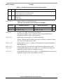
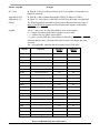
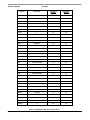
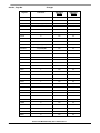
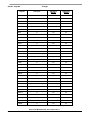
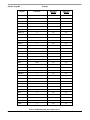
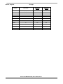
Freescale Semiconductor
Addendum
Document Number: MPC850UMAD
Rev. 1.7, 06/2010
Errata to the MPC850 Family User’s
Manual, Rev. 1
This errata document describes corrections to the MPC850 Family User’s Manual, Revision 1. For
convenience, the section number and page number of the errata item in the reference manual are provided.
Items with section and page numbers in bold are new since the last revision of this document.
To locate any published updates for this document, refer to the world-wide web located on the last page of
this document.
Section/Page
Changes
1, 1-2
For the MPC850DSL part in Table 1-1, change ‘Time-slot assigner, SMC2, and
I2C are not supported.’ to the following:
Time-slot assigner and I2C are not supported.
11.1.3.1, 11-3
Add the following note:
NOTE
The PLL loss of lock detection does not have a specification for the
detection threshold. Therefore, it should be used solely as a debug tool and
not in production systems. Characterization of the threshold value over
temperature and operating voltages has shown that the threshold can be
triggered when clock out to clock in phase differences are 1.8 ns or more.
11.3.1.1, 11-9
In Figure 11-8, change the field description for bit 2 to BBE (boot burst enable)
and the field description for bit 15 to CLES (core little-endian swap).
Add the following description to Table 11-3:
© 2010 Freescale Semiconductor, Inc. All rights reserved.
Section, Page No.
Changes
Table 11-3. Hard Reset Configuration Word Field Descriptions
Bits
Name
Description
2
BBE
Boot burst enable
0 The boot device does not support bursting.
1 The boot device does support bursting.
15
CLES
Core little-endian swap. Defines core access operation following reset.
0 Big endian
1 Little endian
14.2.2.3, 14-8
Replace Table 14-2 with the following:
Table 14-2. XFC Capacitor Values Based on PLPRCR[MF]
MF Range
Minimum Capacitance
1 ≤ (MF + 1) ≤ 4 XFC = [(MF + 1) × 425] – 125
(MF + 1) > 4
15.4.1,15-9
15.4.2, 15-11
15.8.4, 15-55
18.6.3, 18-13
21.2.1, 21-9
21.2.1, 21-9
XFC = (MF + 1) × 520
Maximum Capacitance
Unit
XFC = [(MF + 1) × 590] – 175
pF
XFC = (MF + 1) × 920
pF
In Figure 16-6, BR0, add the following footnote:
Since the base address value is unknown at reset, program BR0 before
programming OR0 to ensure proper operation.
Replace the text after Figure 16-7 with the following:
At reset, OR0 has specific default values and is read-only, as shown in Figure
15-8. After reset, OR0 becomes R/W.
Remove Section 15.8.4.1, “Address Incrementing for External Synchronous
Bursting Masters.”
Remove Table 18-10 as well as the sentence before and the sentence after.
In the MODE field (bits 28–31) of Table 21-2, V.14 RAM microcode is not
supported. Thereby, mode 0111 should be reserved.
In the MODE field (bits 28-31) of Table 21-2, DDCMP RAM microcode is not
supported. Thereby, mode 1001 should be reserved.
Errata to the MPC850 Family User’s Manual, Rev. 1
2
Freescale Semiconductor
Section, Page No.
21.2.4, 21-10
21.3, 21-11
22, 22-1
22.16, 22-14
27.7, 27-9
27.21, 27-23
28.8, 28-7
31.4.1.2, 31-9
34.1, 34-2
34.3, 34-8
34.5.1.2, 34-18
35.2.1, 35-4
Changes
In Figure 21-5, change the TODR register access from R/W to W (write only).
Also, in Table 21-3, revise the second sentence of bit setting 1 in the TODR[TOD]
description to read “TOD is cleared automatically after one system clock cycle,
but...”
In addition, in Table 21-3, “TODR Field Descriptions,” in TOD field description,
change “TOD is cleared automatically after one serial clock...” to say “TOD is
cleared automatically after 1 system clock...”
Under third bullet point, change “For an RxBD, the value must be even,” to say,
“For an RxBD, the value must be mod 4 aligned.”
The last sentence in the last paragraph should be removed.
In the RZS field (bit 7) of Table 22-9, for selection 1, the second sentence in the
paragraph (making reference to V.14 applications) should be removed.
Add superscript number 2 after PADDR1_H, PADDR1_M, PADDR1_L,
TADDR_H, TADDR_M, and TADDR_L. Add the corresponding footnote 2 at the
end of Table 27-1 with the following statement:
The address should be written in little endian, not Motorola’s big-endian format,
that is, physical address 112233445566 should be written PADDR_L = 6655,
PADDR_M = 4433, and PADDR_H = 2211. The TADDR should be written in the
same way as the PADDR.
In step 26, change the last sentence to read, “Then write 0x000E to
TxBD[Data... .”
In Table 28-5, change the third sentence in the Transmitter Underrun description
to read as follows:
Underrun in transparent mode occurs when the CPM or SDMA is experiencing a
latency issue and cannot keep up with the transmission rate.
In the last sentence of Example 1, change the order of the string for REV = 1 to
the following:
first
j_klmn_r_stuv
last
In the last sentence of Example 3, change the order of the string for REV = 1 to
the following:
first
r_stuv_ghij_klmn last
Inside the second bullet, add a footnote at the end of the sentence that states:
At power on reset, port pins are not defined in any particular state until CLKOUT
is present for two clocks.
In Table 34-6, add RTS2 to PB18, PBPAR[DDn] = 1, and PBDIR[DRn] = 1.
In Table 34-19, in the description of bits 3–15, add the following footnote to the
definition of setting to 1 (The corresponding signal is an output):
PD8 and PD10 will function as open drain.
The first bullet should reflect SPS = 0, and the second bullet should reference SPS = 1.
Errata to the MPC850 Family User’s Manual, Rev. 1
Freescale Semiconductor
3
Section, Page No.
B.3.1, B-4
Appendix B, B-4
Appendix F, F-2
Global
Legend:
Changes
In Table B-1, the row making reference to SCC in Profibus (seventeenth row)
should be removed.
In Table B-1, add a column showing that USB is 24 Mbps at 25 MHz.
In Figure F-1, add a line over the block for SMC2 to show that it is supported.
The following table is provided to clarify/correct the power-on reset value of
many of the MPC850 registers and lists whether each register is affected by
HRESET and/or SRESET.
x or X = ‘don’t care’ in either bits, nibbles, or the entire register.
0 = a single zero indicates the entire register is reset to zeros.
( ) = isolates bits of a nibble of the register.
? = a don’t care for POR, but if this register is affected by HRESET or SRESET,
indicates that the value will remain the same as what it was before the reset
occurred.
NA = not applicable, indicates that this register has no POR value.
POR Value
Affected by
HRESET
Affected by
SRESET
SIUMCR
01200000
Yes
No
SYPCR
FFFFFF07
Yes
No
SWSR
0
Yes
Yes
SIPEND
0000xxxx
Yes
Yes
SIMASK
0000xxxx
Yes
Yes
SIEL
0000xxxx
Yes
No
SIVEC
(xx11)(11xx)xxxxxx
Yes
Yes
TESR
XXXX0000
Yes
Yes
SDCR
0
Yes
No
PBR0
x
No
No
POR0
x
No
No
PBR1
x
No
No
POR1
x
No
No
PBR2
x
No
No
POR2
x
No
No
PBR3
x
No
No
POR3
x
No
No
PBR4
x
No
No
POR4
x
No
No
PBR5
x
No
No
POR5
x
No
No
Register
Errata to the MPC850 Family User’s Manual, Rev. 1
4
Freescale Semiconductor
Section, Page No.
Changes
POR Value
Affected by
HRESET
Affected by
SRESET
PBR6
x
No
No
POR6
x
No
No
PBR7
x
No
No
POR7
x
No
No
PGCRA
0
Yes
No
PGCRBf
0
Yes
No
PSCR
x
No
No
PIPR
??00??00
Yes
Yes
PER
0
Yes
Yes
BR0
XXXXX(??00)0(000?)
Yes
No
OR0
00000FF4
Yes
No
BR1
XXXXXX(xx00)0
Yes
No
OR1
XXXXXXX(xxx0)
Yes
No
BR2
XXXXXX(xx00)0
Yes
No
OR2
XXXXXXX(xxx0)
Yes
No
BR3
XXXXXX(xx00)0
Yes
No
OR3
XXXXXXX(xxx0)
Yes
No
BR4
XXXXXX(xx00)0
Yes
No
OR4
XXXXXXX(xxx0)
Yes
No
BR5
XXXXXX(xx00)0
Yes
No
OR5
XXXXXXX(xxx0)
Yes
No
BR6
XXXXXX(xx00)0
Yes
No
OR6
XXXXXXX(xxx0)
Yes
No
BR7
XXXXXX(xx00)0
Yes
No
OR7
XXXXXXX(xxx0)
Yes
No
MAR
x
No
No
MCR
(xx00)0(x000)0(xxx0)X(00xx)X
Yes
No
MAMR
xx001000
Yes
No
MBMR
xx001000
Yes
No
MSTAT
0
Yes
No
MPTPR
0200
Yes
No
MDR
x
No
No
TBSCR
0
Yes
No
Register
Errata to the MPC850 Family User’s Manual, Rev. 1
Freescale Semiconductor
5
Section, Page No.
Changes
POR Value
Affected by
HRESET
Affected by
SRESET
TBREFA
x
No
No
TBREFB
x
No
No
RTCSC
00(000x)(000x)
Yes
Yes
RTC
x
No
Yes
RTSEC
x
No
Yes
RTCAL
x
No
No
PISCR
0
Yes
No
PITC
x
No
No
PITR
x
N/A
N/A
SCCR
0(000?)(?000)(0??0)0000
Yes
No
???0(0100)000
Yes
Yes
RSR
0
Yes
Yes
TBSCRK
x
Yes
Yes
TBREFAK
x
Yes
Yes
TBREFBK
x
Yes
Yes
TBK
x
Yes
Yes
RTCSCK
x
Yes
Yes
RTCK
x
Yes
Yes
RTSECK
x
Yes
Yes
RTCALK
x
Yes
Yes
PISCRK
x
Yes
Yes
PITCK
x
Yes
Yes
SCCRK
x
Yes
Yes
PLPRCRK
x
Yes
Yes
RSRK
x
Yes
Yes
I2MOD
0
Yes
Yes
I2ADD
x
No
No
I2BRG
FFFF
Yes
No
I2COM
0
Yes
Yes
I2CER
0
Yes
Yes
I2CMR
0
Yes
Yes
SDAR
x
No
No
SDSR
0
Yes
Yes
Register
PLPRCR
Errata to the MPC850 Family User’s Manual, Rev. 1
6
Freescale Semiconductor
Section, Page No.
Changes
POR Value
Affected by
HRESET
Affected by
SRESET
SDMR
0
Yes
Yes
IDSR1
0
Yes
Yes
IDMR1
0
Yes
Yes
IDSR2
0
Yes
Yes
IDMR2
0
Yes
Yes
CIVR
0
Yes
Yes
CICR
0
Yes
No
CIPR
0
Yes
Yes
CIMR
0
Yes
Yes
CISR
0
Yes
Yes
PADIR
0
Yes
No
PAPAR
0
Yes
No
PAODR
0
Yes
No
PADAT
x
No
No
PCDIR
0
Yes
No
PCPAR
0
Yes
No
PCSO
0
Yes
No
PCDAT
x
No
No
PCINT
0
Yes
No
PDDIR
0
Yes
No
PDPAR
0
Yes
No
PDDAT
x
No
No
TGCR
0
Yes
Yes
TMR1
0
Yes
Yes
TMR2
0
Yes
Yes
TRR1
FFFF
Yes
Yes
TRR2
FFFF
Yes
Yes
TCR1
0
Yes
Yes
TCR2
0
Yes
Yes
TCN1
0
Yes
Yes
TCN2
0
Yes
Yes
TMR3
0
Yes
Yes
TMR4
0
Yes
Yes
Register
Errata to the MPC850 Family User’s Manual, Rev. 1
Freescale Semiconductor
7
Section, Page No.
Changes
POR Value
Affected by
HRESET
Affected by
SRESET
TRR3
FFFF
Yes
Yes
TRR4
FFFF
Yes
Yes
TCR3
0
Yes
Yes
TCR4
0
Yes
Yes
TCN3
0
Yes
Yes
TCN4
0
Yes
Yes
TER1
0
Yes
Yes
TER2
0
Yes
Yes
TER3
0
Yes
Yes
TER4
0
Yes
Yes
CPCR
0
Yes
Yes
RCCR
0
Yes
No
RCTR1
NA
Yes
Yes
RCTR2
NA
Yes
Yes
RCTR3
NA
Yes
Yes
RCTR4
NA
Yes
Yes
RTER
0
Yes
Yes
RTMR
0
Yes
Yes
BRGC1
0
Yes
No
BRGC2
0
Yes
No
BRGC3
0
Yes
No
BRGC4
0
Yes
No
GSMR_L1
0
Yes
Yes
GSMR_H1
0
Yes
Yes
PSMR1
0
Yes
Yes
TODR1
0
Yes
Yes
7E7E
Yes
Yes
SCCE1
0
Yes
Yes
SCCM1
0
Yes
Yes
SCCS1
0
Yes
Yes
GSMR_L2
0
Yes
Yes
GSMR_H2
0
Yes
Yes
PSMR2
0
Yes
Yes
Register
DSR1
Errata to the MPC850 Family User’s Manual, Rev. 1
8
Freescale Semiconductor
Section, Page No.
Changes
POR Value
Affected by
HRESET
Affected by
SRESET
0
Yes
Yes
7E7E
Yes
Yes
SCCE2
0
Yes
Yes
SCCM2
0
Yes
Yes
SCCS2
0
Yes
Yes
GSMR_L3
0
Yes
Yes
GSMR_H3
0
Yes
Yes
PSMR3
0
Yes
Yes
TODR3
0
Yes
Yes
7E7E
Yes
Yes
SCCE3
0
Yes
Yes
SCCM3
0
Yes
Yes
SCCS3
0
Yes
Yes
GSMR_L4
0
Yes
Yes
GSMR_H4
0
Yes
Yes
PSMR4
0
Yes
Yes
TODR4
0
Yes
Yes
7E7E
Yes
Yes
SCCE4
0
Yes
Yes
SCCM4
0
Yes
Yes
SCCS4
0
Yes
Yes
SMCMR1
0
Yes
Yes
SMCE1
0
Yes
Yes
SMCM1
0
Yes
Yes
SMCMR2
0
Yes
Yes
SMCE2
0
Yes
Yes
SMCM2
0
Yes
Yes
SPMODE
0
Yes
Yes
SPIE
0
Yes
Yes
SPIM
0
Yes
Yes
SPCOM
0
Yes
Yes
PIPC
0
Yes
No
PTPR
0
Yes
No
Register
TODR2
DSR2
DSR3
DSR4
Errata to the MPC850 Family User’s Manual, Rev. 1
Freescale Semiconductor
9
Section, Page No.
Changes
POR Value
Affected by
HRESET
Affected by
SRESET
PBDIR
xxx(xx00)0000
Yes
No
PBPAR
xxx(xx00)0000
Yes
No
PBODR
0
Yes
No
PBDAT
x
Yes
Yes
SIMODE
0
Yes
Yes
SIGMR
0
Yes
No
SISTR
0
Yes
No
SICMR
0
Yes
Yes
SICR
0
Yes
No
SIRP
0
Yes
Yes
Register
Errata to the MPC850 Family User’s Manual, Rev. 1
10
Freescale Semiconductor
How to Reach Us:
Home Page:
www.freescale.com
Web Support:
http://www.freescale.com/support
USA/Europe or Locations Not Listed:
Freescale Semiconductor, Inc.
Technical Information Center, EL516
2100 East Elliot Road
Tempe, Arizona 85284
1-800-521-6274 or
+1-480-768-2130
www.freescale.com/support
Europe, Middle East, and Africa:
Freescale Halbleiter Deutschland GmbH
Technical Information Center
Schatzbogen 7
81829 Muenchen, Germany
+44 1296 380 456 (English)
+46 8 52200080 (English)
+49 89 92103 559 (German)
+33 1 69 35 48 48 (French)
www.freescale.com/support
Information in this document is provided solely to enable system and software
implementers to use Freescale Semiconductor products. There are no express or
implied copyright licenses granted hereunder to design or fabricate any integrated
circuits or integrated circuits based on the information in this document.
Freescale Semiconductor reserves the right to make changes without further notice to
any products herein. Freescale Semiconductor makes no warranty, representation or
guarantee regarding the suitability of its products for any particular purpose, nor does
Freescale Semiconductor assume any liability arising out of the application or use of
any product or circuit, and specifically disclaims any and all liability, including without
limitation consequential or incidental damages. “Typical” parameters which may be
provided in Freescale Semiconductor data sheets and/or specifications can and do
vary in different applications and actual performance may vary over time. All operating
parameters, including “Typicals” must be validated for each customer application by
customer’s technical experts. Freescale Semiconductor does not convey any license
Japan:
Freescale Semiconductor Japan Ltd.
Headquarters
ARCO Tower 15F
1-8-1, Shimo-Meguro, Meguro-ku
Tokyo 153-0064
Japan
0120 191014 or
+81 3 5437 9125
[email protected]
under its patent rights nor the rights of others. Freescale Semiconductor products are
Asia/Pacific:
Freescale Semiconductor China Ltd.
Exchange Building 23F
No. 118 Jianguo Road
Chaoyang District
Beijing 100022
China
+86 10 5879 8000
[email protected]
claims, costs, damages, and expenses, and reasonable attorney fees arising out of,
For Literature Requests Only:
Freescale Semiconductor
Literature Distribution Center
1-800 441-2447 or
+1-303-675-2140
Fax: +1-303-675-2150
LDCForFreescaleSemiconductor
@hibbertgroup.com
Document Number: MPC850UMAD
Rev. 1.7
06/2010
not designed, intended, or authorized for use as components in systems intended for
surgical implant into the body, or other applications intended to support or sustain life,
or for any other application in which the failure of the Freescale Semiconductor product
could create a situation where personal injury or death may occur. Should Buyer
purchase or use Freescale Semiconductor products for any such unintended or
unauthorized application, Buyer shall indemnify and hold Freescale Semiconductor
and its officers, employees, subsidiaries, affiliates, and distributors harmless against all
directly or indirectly, any claim of personal injury or death associated with such
unintended or unauthorized use, even if such claim alleges that Freescale
Semiconductor was negligent regarding the design or manufacture of the part.
Freescale, the Freescale logo, and PowerQUICC, are trademarks of
Freescale Semiconductor, Inc. Reg. U.S. Pat. & Tm. Off. All other product
or service names are the property of their respective owners. The Power
Architecture and Power.org word marks and the Power and Power.org logos
and related marks are trademarks and service marks licensed by
Power.org.
© 2010 Freescale Semiconductor, Inc.