1
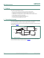
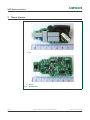
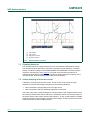
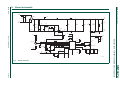
UM10474 SSL2103 230 V 12 W E27 retrofit LED driver demo board Rev. 1 — 19 July 2011 User manual Document information Info Content Keywords SSL2103, LED driver, main dimmable, non-isolated, AC/DC Abstract User manual for the SSL2103 12 W Buck demo board UM10474 NXP Semiconductors SSL2103 230 V 12 W E27 retrofit LED driver demo board Revision history Rev Date Description v.1 20110719 first issue Contact information For more information, please visit: http://www.nxp.com For sales office addresses, please send an email to: [email protected] UM10474 User manual All information provided in this document is subject to legal disclaimers. Rev. 1 — 19 July 2011 © NXP B.V. 2011. All rights reserved. 2 of 21 UM10474 NXP Semiconductors SSL2103 230 V 12 W E27 retrofit LED driver demo board 1. Introduction WARNING Lethal voltage and fire ignition hazard The non-insulated high voltages that are present when operating this product, constitute a risk of electric shock, personal injury, death and/or ignition of fire. This product is intended for evaluation purposes only. It shall be operated in a designated test area by personnel qualified according to local requirements and labor laws to work with non-insulated mains voltages and high-voltage circuits. This product shall never be operated unattended. This SSL2103 user manual is intended for 230 V applications of 12 W demo boards of E27-type (and similar type) retrofit light sources. The circuit implements a Boundary Conduction Mode (BCM) buck converter. It is mains dimmable for both forward phase (triac) dimmers, and reverse phase (transistor) dimmers. It is designed for demonstrating high performance and high efficiency. It produces a 400 mA regulated output current to drive 10 LEDs at a 230 V (AC) input. With the help of an external MOSFET, an efficiency of up to 85 % can be achieved. This demo board is connected to a high AC voltage (up to 265 V). Avoid touching the demo board during operation. An isolated housing is obligatory when used in uncontrolled, non-laboratory environments. Galvanic isolation of the mains phase using a fixed or variable transformer (Variac) is always recommended. These devices are recognized by the symbols shown in Figure 1. 019aab174 019aab173 a. Isolated Fig 1. UM10474 User manual b. Not isolated Variac isolation symbols All information provided in this document is subject to legal disclaimers. Rev. 1 — 19 July 2011 © NXP B.V. 2011. All rights reserved. 3 of 21 UM10474 NXP Semiconductors SSL2103 230 V 12 W E27 retrofit LED driver demo board 2. Features Key reference board features include: • • • • • • Buck converter operating in Boundary Conduction Mode (BCM) Designed to operate with an input voltage of 230 V at 50 Hz, 10 % Optimized for an output power of 12 W (10 LEDs) at 400 mA output current Active damper and inrush current limiter Main dimmable with leading and trailing dimmers Intrinsically protected against short circuit 3. Connecting the board The board is designed for a 230 V (AC), 50 Hz mains supply. This application is optimized for a 12 W LED load (10 LEDs), the output voltage must not exceed 35 V. Do not supply the board without the LED load because this damages the protection Zener diode (D8, see Figure 5). LED+ neutral LED- line 019aac542 Fig 2. Board connections Place the galvanic isolated transformer between the AC source and the dimmer/demo board. Connect the string of 10 LEDs as shown in Figure 2. UM10474 User manual All information provided in this document is subject to legal disclaimers. Rev. 1 — 19 July 2011 © NXP B.V. 2011. All rights reserved. 4 of 21 UM10474 NXP Semiconductors SSL2103 230 V 12 W E27 retrofit LED driver demo board 4. Specifications Table 1 gives the specifications for the SSL2103 12 W LED driver. Table 1. UM10474 User manual Specifications Description Value Comment AC line input voltage 200 V (AC) to 260 V (AC) optimized for 230 V (AC) with 10 % variation output voltage (LED voltage) 31 V (DC) load = 10 LEDs output voltage protection 36 V (DC) by Zener diode output power (LED power) 12.5 W load = 10 LEDs efficiency > 85 % at Tamb = 25 C, nominal input voltage (see Figure 9). power factor > 0.8 at nominal input voltage (See Figure 8). output current (LED current) 400 mA at Tamb = 25 C, nominal input voltage. load current accuracy/ input voltage dependency < 10 % at Tamb = 25 C; Vi = 230 V (AC), 10 % (see Figure 7) output current ripple 120 mA see Figure 12 switching frequency 30 kHz nominal frequency dimming range 100 % to 10 % for triac dimmer board dimensions (l w h) 63 mm 32 mm 18 mm operating temperature 0 C to 70 C EMC compliance EN55015 All information provided in this document is subject to legal disclaimers. Rev. 1 — 19 July 2011 conducted emissions © NXP B.V. 2011. All rights reserved. 5 of 21 UM10474 NXP Semiconductors SSL2103 230 V 12 W E27 retrofit LED driver demo board 5. Board photos 019aac543 a. Top 019aac544 b. Bottom Fig 3. UM10474 User manual Board photos All information provided in this document is subject to legal disclaimers. Rev. 1 — 19 July 2011 © NXP B.V. 2011. All rights reserved. 6 of 21 UM10474 NXP Semiconductors SSL2103 230 V 12 W E27 retrofit LED driver demo board 6. Dimmers NXP Semiconductors has tested numerous dimmers for compatibility. The dimming performance of the board may vary as different dimmers have different specifications. Table 2 and Table 3 show the range of dimmers that have been tested and found to be compatible with the board. Table 2. Manufacturer Type Voltage (V (AC)) Power range Load (W) Berker 2819 230 60 to 400 incandescent Berker 2873 230 20 to 500 halogen/incandescent Bush-Jaeger 2250U 230 60 to 600 halogen/incandescent Bush-Jaeger 2200U 230 60 to 400 incandescent Ehmann T10 230 60 to 300 incandescent Gira 0300 230 60 to 400 incandescent Gira 1184 230 60 to 400 incandescent Opus 852.390 230 60 to 400 incandescent Table 3. UM10474 User manual TRIAC dimmers Transistor dimmers Manufacturer Type Voltage (V (AC)) Power range Load (W) Jung 243 EX 230 20 to 360 halogen/incandescent Jung 225 TDE 230 20 to 525 halogen/incandescent Berker 2874 230 20 to 525 halogen/incandescent Berker 286710 230 20 to 360 halogen/incandescent Bush-Jaeger 6513U 230 40 to 420 halogen/incandescent Gira 0307 230 20 to 525 halogen/incandescent PEHA 433 HAB 230 20 to 315 halogen/incandescent Legrand 784.06 230 40 to 300 halogen/incandescent All information provided in this document is subject to legal disclaimers. Rev. 1 — 19 July 2011 © NXP B.V. 2011. All rights reserved. 7 of 21 UM10474 NXP Semiconductors SSL2103 230 V 12 W E27 retrofit LED driver demo board 7. Functional description The IC SSL2103 is an extension to the SSL2101/SSL2102 platform and gives designers the flexibility to use any power level by controlling external switches. In this application, it controls the buck converter part and ensures proper dimmer operation. One of these switches controls the buck operation and is opened when the voltage on the SOURCE pin exceeds 0.5 V. When dimmers are used, the circuit detects the rectified voltage change and reduces the duty cycle and oscillator frequency to reduce the output current. The circuit has a bleeding circuit that can drive two external current sinks: the weak bleeder (pin WB_DRV) and the strong bleeder (pin SB_DRV). When the voltage on the HVDET pin drops below a certain value (52 V typical), the strong bleeder command is on. This state provides a current path that loads the dimmer during zero voltage crossing. The dimmer timer is reset. When the voltage on the HVDET pin exceeds 52 V and the voltage on pin ISENSE exceeds 100 mV, the weak bleeder command switches on. This provides a current path that loads the dimmer while the converter draws insufficient current to stabilize the dimmer latching. In this application, both bleeder commands activate the same bipolar transistor (T1) using two different base currents to drive it. 50 mA for the strong bleeder and 20 mA for the weak bleeder. The strong bleeder always switches while the weak bleeder does not switch on until the output power drops in a dimmed operation. It allows the system to operate with the majority of field installed dimmers. Figure 4 shows the bleeder drive outputs in a dimmed operation. UM10474 User manual All information provided in this document is subject to legal disclaimers. Rev. 1 — 19 July 2011 © NXP B.V. 2011. All rights reserved. 8 of 21 UM10474 NXP Semiconductors SSL2103 230 V 12 W E27 retrofit LED driver demo board (1) (2) (3) (4) 019aac545 (1) Input voltage (2) Input current (3) WB_DRV command (4) SB_DRV command Fig 4. Dimmed bleeder operation 7.1 Dimming detection The dimming reference voltage is derived from a non-buffered rectified mains voltage. The dimming range is detected by sensing the average rectified voltage by a resistive divider. Use the the voltage on pins BRIGHTNESS and PWMLIMIT to set the converter duty factor and frequency (see Figure 5). The peak current through the inductor is reduced by balancing the voltage levels at these two inputs before the frequency of the converter drops, thus eliminating audible noise from the winding. 7.2 Active damping and inrush current A damper is required to limit inrush current. Inrush current occurs when the input capacitors encounter fast voltage changes as in the following situations: • When the board is hot-plugged into an AC input source. • When the board is fed from a leading-edge phase cut dimmer. There are many ways to perform damping. A single resistor is the cheapest solution but it can lead to thermal issues and low efficiency. The damper resistor has a major impact on the power losses of the system. At low power ratings (< 10 W), a serial resistor is suitable because the losses are acceptable. At higher power ratings, an active circuit becomes the preferred solution to achieve high efficiency. UM10474 User manual All information provided in this document is subject to legal disclaimers. Rev. 1 — 19 July 2011 © NXP B.V. 2011. All rights reserved. 9 of 21 UM10474 NXP Semiconductors SSL2103 230 V 12 W E27 retrofit LED driver demo board The solution applied here is an active damper using a MOSFET transistor (T3). T3 is used to bypass damping resistors R5 and R6 following inrush current. The MOSFET is ON when the current in the circuit is low enough to keep the bipolar transistor Q1 from pulling down the gate of the MOSFET (T3) (see Figure 5). UM10474 User manual All information provided in this document is subject to legal disclaimers. Rev. 1 — 19 July 2011 © NXP B.V. 2011. All rights reserved. 10 of 21 xxxxxxxxxxxxxxxxxxxxx xxxxxxxxxxxxxxxxxxxxxxxxxx xxxxxxx x x x xxxxxxxxxxxxxxxxxxxxxxxxxxxxxx xxxxxxxxxxxxxxxxxxx xx xx xxxxx xxxxxxxxxxxxxxxxxxxxxxxxxxx xxxxxxxxxxxxxxxxxxx xxxxxx xxxxxxxxxxxxxxxxxxxxxxxxxxxxxxxxxxx xxxxxxxxxxxx x x xxxxxxxxxxxxxxxxxxxxx xxxxxxxxxxxxxxxxxxxxxxxxxxxxxx xxxxx xxxxxxxxxxxxxxxxxxxxxxxxxxxxxxxxxxxxxxxxxxxxxxxxxx xxxxxxxx xxxxxxxxxxxxxxxxxxxxxxxxx xxxxxxxxxxxxxxxxxxxx xxx TP1 line F1 1A C4 220 nF (310 V) D5 MBS6 C6 470 pF TP3 neutral Vrect R15 2.2 kΩ 2W L2 D7 TP4 LED+ ELC10D182E RS1J R33 82 kΩ R32 82 kΩ D10 SMAJ400A D12 R30 BAV21WS-V 300 kΩ Q1 MMBT2222A D11 BZX84-C15 C17 1 nF RGND C18 100 nF C2 150 nF (300 V) 3 2 1 C20 47 nF R10 R6 120 Ω 2W R18 2 4 2 A R19 43 kΩ BAS28 R16 2 3 SB_DRV 3.9 kΩ 1 4 WB_DRV R23 56 kΩ C19 1.5 nF 3 R11 100 Ω A R7 R26 C12 D6 BZX384-C4V7 C7 10 nF RC 220 kΩ R29 6.8 kΩ 330 pF RC2 BRIGHTNESS PWMLIMIT C9 1 nF R20 22 kΩ 100 Ω ISENSE D3 1 kΩ C14 D1 R1 BAV21WS-V 100 Ω U1 1 Vrect Vrect D9 R27 180 kΩ BZD27C 150P 200 kΩ 9.1 kΩ R28 13 kΩ C13 4.7 μF (25 V) VCC 3 2 7 12 6 11 5 8 R24 14 13 9 R25 R22 5 100 nF C15 R14 TP2 LED- 1 CSV-RM6S_1S-6P-G VCC 100 nF 1 L1 3 R5 120 Ω 2W 2 R35 10 kΩ 10 Ω R4 560 Ω 1W 4 D8 BZG03C36 C10 1000 μF (35 V) D4 ES2G T3 BSP298 1 3 R3 560 Ω 1W PBHV8140Z C3 100 nF (310 V) 4 10 GND HVDET DRAIN PWR_DRV VCC C1 47 μF (25 V) D2 BZX384-C24 R21 10 Ω AUX R9 10 Ω T2 R17 2 1 IPD60R385CP 10 Ω SOURCE 3 AUX R2 47 kΩ R13 1.5 Ω R8 1.2 Ω R12 1.2 Ω C8 100 pF AUX 1 kΩ C16 1 nF C11 1 nF 019aac546 Board schematic UM10474 11 of 21 © NXP B.V. 2011. All rights reserved. SSL2103 230 V 12 W E27 retrofit LED driver demo board Rev. 1 — 19 July 2011 All information provided in this document is subject to legal disclaimers. Vrect C5 100 nF (310 V) R31 1 kΩ 2.2 Ω Fig 5. NXP Semiconductors UM10474 User manual 8. Board schematic UM10474 NXP Semiconductors SSL2103 230 V 12 W E27 retrofit LED driver demo board 9. Bill Of Materials (BOM) Table 4. Bill of materials Part Ref. Value no. Power Tolerance Voltage (W) (%) (V) Package SMD Type Manufacturer 1 1A - - N 0263001.HAT1L Littelfuse F1 - - 2 R1 100 0.5 5 200 1206 Y - - 3 R2 47 k 0.25 5 150 0805 Y - - 4 R3 560 2 5 350 - N MFP2 Welwyn 5 R4 560 2 5 350 - N MFP2 Welwyn 6 R5 120 2 5 350 - N MFP2 Welwyn 7 R6 120 2 5 350 - N MFP2 Welwyn 8 R7 100 0.5 5 200 1206 Y - - 9 R8 1.2 0.5 5 200 1206 Y - - 10 R9 10 0.25 5 150 0805 Y - - 11 R10 2.2 0.5 5 200 1206 Y - - 12 R11 100 0.5 5 200 1206 Y - - 13 R12 1.2 0.5 5 200 1206 Y - - 14 R13 1.5 0.5 5 200 1206 Y - - 15 R14 56 k 0.1 1 50 0603 Y - - 16 R15 2.2 k 2 5 300 - Y - - 17 R16 3.9 k 0.1 1 50 0603 Y - - 18 R17 10 0.25 5 150 0805 Y - - 19 R18 10 0.5 1 400 2010 Y - - 20 R19 43 k 0.1 1 50 0603 Y - - 21 R20 22 k 0.1 1 50 0603 Y - - 22 R21 10 0.25 5 150 0805 Y - - 23 R22 180 k 0.25 5 150 0805 Y - - 24 R23 1 k 0.1 1 50 0603 Y - - 25 R24 1 k 0.1 1 50 0603 Y - - 26 R25 9.1 k 0.1 1 50 0603 Y - - 27 R26 220 k 0.1 1 50 0603 Y - - 28 R27 200 k 0.25 5 150 0805 Y - - 29 R28 13 k 0.1 1 50 0603 Y - - 30 R29 6.8 k 0.1 1 50 0603 Y - - 31 R30 300 k 0.1 1 50 0603 Y - - 32 R31 1 k 0.1 1 50 0603 Y - - 33 R32 82 k 0.5 5 200 1206 Y - - 34 R33 82 k 0.5 5 200 1206 Y - - 35 R35 10 k 0.25 5 150 0805 Y - - 36 C1 47 F - 10 25 2917 N TR3D476K025C0150 Vishay 37 C2 150 nF - 20 300 Poly N BFC233841154 Vishay 38 C3 100 nF - 20 300 Poly N BFC233841104 Vishay UM10474 User manual All information provided in this document is subject to legal disclaimers. Rev. 1 — 19 July 2011 © NXP B.V. 2011. All rights reserved. 12 of 21 UM10474 NXP Semiconductors SSL2103 230 V 12 W E27 retrofit LED driver demo board Table 4. Bill of materials …continued Part Ref. Value no. Power Tolerance Voltage (W) (%) (V) Package SMD Type Manufacturer 39 C4 220 nF - 20 310 Poly N BFC233922224 Vishay 40 C5 100 nF - 20 300 Poly N BFC233841104 Vishay 41 C6 470 pF - 10 250 2211 Y GA352QR7GF471KW01L Murata 42 C7 10 nF - 10 50 0603 Y - - 43 C8 100 pF - 10 50 0603 Y - - 44 C9 1 nF - 10 50 0603 Y - - 45 C10 1000 F - 20 35 Radial N EEUFM1V102 Panasonic 46 C11 1 nF - 10 50 0603 Y - - 47 C12 330 pF - 10 50 0603 Y - - 48 C13 4.7 F - 10 25 0805 Y - - 49 C14 100 nF - 10 50 0603 Y - - 50 C15 100 nF - 10 50 0603 Y - - 51 C16 1 nF - 10 50 0603 Y - - 52 C17 1 nF - 10 50 0603 Y - - 53 C18 100 nF - 10 50 0603 Y - - 54 C19 1.5 nF - 10 50 0603 Y - - 55 C20 47 nF - 10 50 0603 Y - - 56 L1 1 mH - - - RM6 N 3C90 - 57 L2 1.8 mH - - - Radial N ELC10D182E Panasonic 58 D1 0.2 A 0.2 - 250 SOD323 Y BAV21WS Vishay 59 D2 24 V 0.3 5 - SOD323 Y BZX384-C24 NXP Semiconductors 60 D3 signal 0.25 - 85 SOT143 Y BAS28 NXP Semiconductors 61 D4 2A - - 400 SMB Y ES2G Vishay 62 D5 0.5 A - - 600 TO269AA Y MB6S Vishay 63 D6 4.7 V 0.3 5 - SOD323 Y BZX384-C4V7 NXP 64 D7 1A - - 600 SMA Y RS1J Vishay 65 D8 36 V 3 - - SMA Y BZG03C36 Vishay 66 D9 150 V 0.8 - - DO-219AB Y BZD27C150P Vishay 67 D10 400 V 400 5 400 DO-214AC Y SMAJ400A Littelfuse 68 D11 15 V 0.3 5 - SOD-323 Y BZX384-C15 NXP 69 D12 0.2 A 0.2 - 250 SOD-323 Y BAV21WS Vishay 70 Q1 NPN 0.25 - 40 SOT23 Y MMBT2222A NXP Semiconductors 71 T1 NPN - - 400 SOT223 Y PBHV8140Z NXP Semiconductors 72 T2 MOSFET - - 600 DPAK Y IPD60R385CP Infineon 73 T3 MOSFET - - 400 SOT223 Y BPS298 Infineon 74 U1 - - - SO-14 Y SSL2103 NXP Semiconductors UM10474 User manual - All information provided in this document is subject to legal disclaimers. Rev. 1 — 19 July 2011 © NXP B.V. 2011. All rights reserved. 13 of 21 UM10474 NXP Semiconductors SSL2103 230 V 12 W E27 retrofit LED driver demo board 10. Inductor specification Figure 6 shows the Inductor schematic: 12.7 7.62 3 4 3 2 L1 5 Ns 1 6.5 + 0.15 5 2 019aac547 8.5 1 6 0.7 min. a. Schematic Fig 6. 019aac548 b. Bottom view Inductor schematic 10.1 Winding specification Table 5. Number 1 Winding specification Section Wire Layers Turns Pin Begin End L1 0.355 - 80 2 1 2 tape ISO 0.1 - - - - 3 Ns 0.2 - 40 3 5 4 tape ISO 0.1 - - - - 10.2 Electric characteristics Table 6. Inductance Section Inductance (5 % at 100 mA) L1 1024 H Ns 256 H 10.3 Core and bobbin • Core: RM6S-3C90-AL160 • Bobbin: CSV-RM6S-1S-6P-G UM10474 User manual All information provided in this document is subject to legal disclaimers. Rev. 1 — 19 July 2011 © NXP B.V. 2011. All rights reserved. 14 of 21 UM10474 NXP Semiconductors SSL2103 230 V 12 W E27 retrofit LED driver demo board 11. Appendix 11.1 Output current 019aac552 500 Io (mA) 400 300 200 100 190 Fig 7. 210 230 250 Vi (RMS) 270 Output current as a function of input voltage 11.2 Power factor 019aac550 0.88 PF 0.84 0.80 0.76 0.72 0.68 180 Fig 8. UM10474 User manual 200 220 240 Vi (RMS) 260 Power factor as a function of input voltage All information provided in this document is subject to legal disclaimers. Rev. 1 — 19 July 2011 © NXP B.V. 2011. All rights reserved. 15 of 21 UM10474 NXP Semiconductors SSL2103 230 V 12 W E27 retrofit LED driver demo board 11.3 Efficiency 019aac551 95 η (%) 91 87 83 79 75 190 Fig 9. 210 230 250 Vi (RMS) 270 Efficiency as a function of input voltage 11.4 Dimming curve 019aac549 500 Io (mA) 400 300 200 100 0 110 150 190 230 Vi (RMS) 270 Fig 10. Output current as a function of input voltage UM10474 User manual All information provided in this document is subject to legal disclaimers. Rev. 1 — 19 July 2011 © NXP B.V. 2011. All rights reserved. 16 of 21 UM10474 NXP Semiconductors SSL2103 230 V 12 W E27 retrofit LED driver demo board 11.5 Input current (1) (2) 019aac553 (1) Input voltage (2) Input current Fig 11. Input current and input voltage 11.6 Output ripple current (1) (2) 019aac554 (1) LED current (2) Output voltage Fig 12. Output current and output voltage UM10474 User manual All information provided in this document is subject to legal disclaimers. Rev. 1 — 19 July 2011 © NXP B.V. 2011. All rights reserved. 17 of 21 UM10474 NXP Semiconductors SSL2103 230 V 12 W E27 retrofit LED driver demo board 11.7 Start-up time (2) (1) 019aac555 (1) Input voltage (2) LED current Fig 13. Start-up time to nominal output current: 210 ms 11.8 Conducted EMI Test results per standard EN55015 019aac556 Fig 14. Conducted emissions for line: AC input = 230 V at 50 Hz UM10474 User manual All information provided in this document is subject to legal disclaimers. Rev. 1 — 19 July 2011 © NXP B.V. 2011. All rights reserved. 18 of 21 UM10474 NXP Semiconductors SSL2103 230 V 12 W E27 retrofit LED driver demo board 019aac557 Fig 15. Conducted emissions for neutral: AC input = 230 V at 50 Hz UM10474 User manual All information provided in this document is subject to legal disclaimers. Rev. 1 — 19 July 2011 © NXP B.V. 2011. All rights reserved. 19 of 21 UM10474 NXP Semiconductors SSL2103 230 V 12 W E27 retrofit LED driver demo board 12. Legal information 12.1 Definitions Draft — The document is a draft version only. The content is still under internal review and subject to formal approval, which may result in modifications or additions. NXP Semiconductors does not give any representations or warranties as to the accuracy or completeness of information included herein and shall have no liability for the consequences of use of such information. Export control — This document as well as the item(s) described herein may be subject to export control regulations. Export might require a prior authorization from national authorities. 12.2 Disclaimers Limited warranty and liability — Information in this document is believed to be accurate and reliable. However, NXP Semiconductors does not give any representations or warranties, expressed or implied, as to the accuracy or completeness of such information and shall have no liability for the consequences of use of such information. In no event shall NXP Semiconductors be liable for any indirect, incidental, punitive, special or consequential damages (including - without limitation - lost profits, lost savings, business interruption, costs related to the removal or replacement of any products or rework charges) whether or not such damages are based on tort (including negligence), warranty, breach of contract or any other legal theory. Notwithstanding any damages that customer might incur for any reason whatsoever, NXP Semiconductors’ aggregate and cumulative liability towards customer for the products described herein shall be limited in accordance with the Terms and conditions of commercial sale of NXP Semiconductors. Right to make changes — NXP Semiconductors reserves the right to make changes to information published in this document, including without limitation specifications and product descriptions, at any time and without notice. This document supersedes and replaces all information supplied prior to the publication hereof. Suitability for use — NXP Semiconductors products are not designed, authorized or warranted to be suitable for use in life support, life-critical or safety-critical systems or equipment, nor in applications where failure or malfunction of an NXP Semiconductors product can reasonably be expected to result in personal injury, death or severe property or environmental damage. NXP Semiconductors accepts no liability for inclusion and/or use of NXP Semiconductors products in such equipment or applications and therefore such inclusion and/or use is at the customer’s own risk. Applications — Applications that are described herein for any of these products are for illustrative purposes only. NXP Semiconductors makes no representation or warranty that such applications will be suitable for the specified use without further testing or modification. Customers are responsible for the design and operation of their applications and products using NXP Semiconductors products, and NXP Semiconductors accepts no liability for any assistance with applications or customer product design. It is customer’s sole responsibility to determine whether the NXP Semiconductors product is suitable and fit for the customer’s applications and products planned, as well as for the planned application and use of customer’s third party customer(s). Customers should provide appropriate design and operating safeguards to minimize the risks associated with their applications and products. UM10474 User manual NXP Semiconductors does not accept any liability related to any default, damage, costs or problem which is based on any weakness or default in the customer’s applications or products, or the application or use by customer’s third party customer(s). Customer is responsible for doing all necessary testing for the customer’s applications and products using NXP Semiconductors products in order to avoid a default of the applications and the products or of the application or use by customer’s third party customer(s). NXP does not accept any liability in this respect. Evaluation products — This product is provided on an “as is” and “with all faults” basis for evaluation purposes only. NXP Semiconductors, its affiliates and their suppliers expressly disclaim all warranties, whether express, implied or statutory, including but not limited to the implied warranties of non-infringement, merchantability and fitness for a particular purpose. The entire risk as to the quality, or arising out of the use or performance, of this product remains with customer. In no event shall NXP Semiconductors, its affiliates or their suppliers be liable to customer for any special, indirect, consequential, punitive or incidental damages (including without limitation damages for loss of business, business interruption, loss of use, loss of data or information, and the like) arising out the use of or inability to use the product, whether or not based on tort (including negligence), strict liability, breach of contract, breach of warranty or any other theory, even if advised of the possibility of such damages. Notwithstanding any damages that customer might incur for any reason whatsoever (including without limitation, all damages referenced above and all direct or general damages), the entire liability of NXP Semiconductors, its affiliates and their suppliers and customer’s exclusive remedy for all of the foregoing shall be limited to actual damages incurred by customer based on reasonable reliance up to the greater of the amount actually paid by customer for the product or five dollars (US$5.00). The foregoing limitations, exclusions and disclaimers shall apply to the maximum extent permitted by applicable law, even if any remedy fails of its essential purpose. Safety of high-voltage evaluation products — The non-insulated high voltages that are present when operating this product, constitute a risk of electric shock, personal injury, death and/or ignition of fire. This product is intended for evaluation purposes only. It shall be operated in a designated test area by personnel that is qualified according to local requirements and labor laws to work with non-insulated mains voltages and high-voltage circuits. The product does not comply with IEC 60950 based national or regional safety standards. NXP Semiconductors does not accept any liability for damages incurred due to inappropriate use of this product or related to non-insulated high voltages. Any use of this product is at customer’s own risk and liability. The customer shall fully indemnify and hold harmless NXP Semiconductors from any liability, damages and claims resulting from the use of the product. 12.3 Trademarks Notice: All referenced brands, product names, service names and trademarks are the property of their respective owners. All information provided in this document is subject to legal disclaimers. Rev. 1 — 19 July 2011 © NXP B.V. 2011. All rights reserved. 20 of 21 UM10474 NXP Semiconductors SSL2103 230 V 12 W E27 retrofit LED driver demo board 13. Contents 1 2 3 4 5 6 7 7.1 7.2 8 9 10 10.1 10.2 10.3 11 11.1 11.2 11.3 11.4 11.5 11.6 11.7 11.8 12 12.1 12.2 12.3 13 Introduction . . . . . . . . . . . . . . . . . . . . . . . . . . . . 3 Features . . . . . . . . . . . . . . . . . . . . . . . . . . . . . . . 4 Connecting the board . . . . . . . . . . . . . . . . . . . . 4 Specifications. . . . . . . . . . . . . . . . . . . . . . . . . . . 5 Board photos . . . . . . . . . . . . . . . . . . . . . . . . . . . 6 Dimmers . . . . . . . . . . . . . . . . . . . . . . . . . . . . . . . 7 Functional description . . . . . . . . . . . . . . . . . . . 8 Dimming detection . . . . . . . . . . . . . . . . . . . . . . 9 Active damping and inrush current . . . . . . . . . . 9 Board schematic . . . . . . . . . . . . . . . . . . . . . . . 11 Bill Of Materials (BOM) . . . . . . . . . . . . . . . . . . 12 Inductor specification . . . . . . . . . . . . . . . . . . . 14 Winding specification . . . . . . . . . . . . . . . . . . . 14 Electric characteristics . . . . . . . . . . . . . . . . . . 14 Core and bobbin . . . . . . . . . . . . . . . . . . . . . . . 14 Appendix . . . . . . . . . . . . . . . . . . . . . . . . . . . . . 15 Output current. . . . . . . . . . . . . . . . . . . . . . . . . 15 Power factor . . . . . . . . . . . . . . . . . . . . . . . . . . 15 Efficiency . . . . . . . . . . . . . . . . . . . . . . . . . . . . 16 Dimming curve . . . . . . . . . . . . . . . . . . . . . . . . 16 Input current . . . . . . . . . . . . . . . . . . . . . . . . . . 17 Output ripple current . . . . . . . . . . . . . . . . . . . . 17 Start-up time . . . . . . . . . . . . . . . . . . . . . . . . . . 18 Conducted EMI Test results per standard EN55015. . . . . . . . . . . . . . . . . . . . . . . . . . . . . 18 Legal information. . . . . . . . . . . . . . . . . . . . . . . 20 Definitions . . . . . . . . . . . . . . . . . . . . . . . . . . . . 20 Disclaimers . . . . . . . . . . . . . . . . . . . . . . . . . . . 20 Trademarks. . . . . . . . . . . . . . . . . . . . . . . . . . . 20 Contents . . . . . . . . . . . . . . . . . . . . . . . . . . . . . . 21 Please be aware that important notices concerning this document and the product(s) described herein, have been included in section ‘Legal information’. © NXP B.V. 2011. All rights reserved. For more information, please visit: http://www.nxp.com For sales office addresses, please send an email to: [email protected] Date of release: 19 July 2011 Document identifier: UM10474