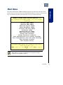
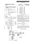
1
Looking for more information?
Visit us on the web at http://www.artisan-scientific.com for more information:
• Price Quotations • Drivers· Technical Specifications. Manuals and Documentation
Artisan Scientific is You~ Source for: Quality New and Certified-Used/Pre:-awned ECJuiflment
• Fast Shipping and DelIve1y
• Tens of Thousands of In-Stock Items
• Equipment Demos
• Hundreds of Manufacturers Supported
• Leasing / Monthly Rentals
Service Center Repairs
Experienced Engineers and Technicians on staff in our
State-of-the-art Full-Service In-House Service Center Facility
• Consignment
InstraView Remote Inspection
Remotely inspect equipment before purchasing with our
Innovative InstraView-website at http://www.instraview.com
We bUy used equipment! We also offer credit for Buy-Backs and Trade-Ins
Sell your excess. underutilized. and idle used equipment. Contact one of our Customer Service Representatives todayl
Talk to a live person: 88EM38-S0URCE fB88-887-68721 I Contact us by email: [email protected] I Visit our website: http://www.artisan-scientific.com
The Endeavor Plus™
Single Board Computer
User’s Guide
Manual PN: 931-0000-03-A
February 2002
Customer Service
Mailing Address:
Post-Sales
Technical Support:
Visit our site at:
ICS Advent
6260 Sequence Drive
San Diego, CA 92121-4371
858-677-0877, option 1
800-480-0044, option 1 (in the U.S. and Canada)
+44 1243 523505 (UK)
0800-91-29-04 (France)
0800-18-30-095 (Germany)
www.icsadvent.com
Information in this document is subject to change without notice.
© 2000 ICS Advent, a California Corporation. All rights reserved.
The information in this document is provided for reference only. ICS Advent does not assume
any liability arising out of the application or use of the information or products described herein.
This document may contain or reference information and products protected by copyrights or
patents and does not convey any license under the patent rights of ICS Advent, nor the rights of
others.
ICS Advent is a Trademark of ICS Advent. All trademarks and registered trademarks are the
property of their respective owners. All rights reserved. Printed in the United States of America.
No part of this publication may be reproduced, stored in a retrieval system, or transmitted, in
any form or by any means, electronic, mechanical, photocopying, recording, or otherwise,
without the prior written permission of the publisher.
Contents
Preface
How to Use This Guide . . . . . . . . . . . . . . . . . . . . . . . . . . . xi
Customer Comments . . . . . . . . . . . . . . . . . . . . . . . . . . . . xii
Advisory Conventions . . . . . . . . . . . . . . . . . . . . . . . . . . . xiii
Safety Instructions . . . . . . . . . . . . . . . . . . . . . . . . . . . . . xiv
When Working Inside a Computer. . . . . . . . . . . . . . xiv
Protecting Against Electrostatic Discharge. . . . . . . xvi
When Operating a Computer . . . . . . . . . . . . . . . . . xvii
Rack Stability . . . . . . . . . . . . . . . . . . . . . . . . . . . . . xviii
Safety Standards. . . . . . . . . . . . . . . . . . . . . . . . . . . xviii
Regulatory Compliance Statements . . . . . . . . . . . . . . . . xix
Guarantee and Warranty Policy. . . . . . . . . . . . . . . . . . . xx
Guarantee . . . . . . . . . . . . . . . . . . . . . . . . . . . . . . . . . xx
Limited Warranty . . . . . . . . . . . . . . . . . . . . . . . . . . . xx
Return Procedure . . . . . . . . . . . . . . . . . . . . . . . . . . . xxi
Limitation of Liability. . . . . . . . . . . . . . . . . . . . . . . xxii
Chapter 1
Introduction
System Features . . . . . . . . . . . . . . . . . . . . . . . . . . . . . . . 1-3
Checklist . . . . . . . . . . . . . . . . . . . . . . . . . . . . . . . . . . . . . 1-6
Product Specifications . . . . . . . . . . . . . . . . . . . . . . . . . . . 1-7
System Architecture . . . . . . . . . . . . . . . . . . . . . . . . . . . 1-10
System Block Diagram . . . . . . . . . . . . . . . . . . . . . . . . . 1-12
Chapter 2
Hardware Settings
Overview . . . . . . . . . . . . . . . . . . . . . . . . . . . . . . . . . . . . .
Jumpers . . . . . . . . . . . . . . . . . . . . . . . . . . . . . . . . . . . . . .
CPU Jumper Settings . . . . . . . . . . . . . . . . . . . . . . . .
Connectors . . . . . . . . . . . . . . . . . . . . . . . . . . . . . . . . . . . .
Pin Assignments . . . . . . . . . . . . . . . . . . . . . . . . . . . .
Manual PN: 931-0000-03-A, February 2002
2-3
2-3
2-4
2-6
2-9
iii
Chapter 3
System Installation
Overview . . . . . . . . . . . . . . . . . . . . . . . . . . . . . . . . . . . . . 3-3
Socket 370 Celeron/Pentium III Processor . . . . . . . . . . 3-3
Installing a CPU. . . . . . . . . . . . . . . . . . . . . . . . . . . . 3-3
Removing a CPU . . . . . . . . . . . . . . . . . . . . . . . . . . . 3-3
Configuring the System Bus . . . . . . . . . . . . . . . . . . 3-4
Main Memory . . . . . . . . . . . . . . . . . . . . . . . . . . . . . . . . . 3-5
Installing the Single Board Computer. . . . . . . . . . . . . . 3-6
AIC-7892 Ultra-160/m SCSI Host Adapter. . . . . . . 3-6
Onboard Intel 810e Graphics Controller. . . . . . . . . 3-7
Intel 82559 Fast Ethernet Controller . . . . . . . . . . . 3-7
Onboard LED Indicator . . . . . . . . . . . . . . . . . . . . . . 3-8
810e Chipset & ATA-66 . . . . . . . . . . . . . . . . . . . . . . 3-8
Winbond Hardware Doctor Software . . . . . . . . . . . 3-9
Flash BIOS . . . . . . . . . . . . . . . . . . . . . . . . . . . . . . . . 3-9
M-systems Flash Disk . . . . . . . . . . . . . . . . . . . . . . . . . 3-10
Installing DiskOnChip (DOC) . . . . . . . . . . . . . . . . 3-10
Watchdog Timer (WDT) Programming . . . . . . . . . . . . 3-11
Enable WDT Function . . . . . . . . . . . . . . . . . . . . . . 3-11
Initialize, Re-trigger, and Stop WDT . . . . . . . . . . 3-11
Clear CMOS Operation . . . . . . . . . . . . . . . . . . . . . . . . 3-12
Power Switch Setup . . . . . . . . . . . . . . . . . . . . . . . . . . . 3-13
Chapter 4
BIOS Setup Information
Overview . . . . . . . . . . . . . . . . . . . . . . . . . . . . . . . . . . . . . 4-3
Entering Setup . . . . . . . . . . . . . . . . . . . . . . . . . . . . . . . . 4-3
Main Menu . . . . . . . . . . . . . . . . . . . . . . . . . . . . . . . . . . . 4-5
Advanced CMOS Setup Reference Tables . . . . . . . . . . . 4-6
Standard CMOS Setup Menu. . . . . . . . . . . . . . . . . . . . 4-17
Advanced CMOS Setup Menu . . . . . . . . . . . . . . . . . . . 4-17
Advanced Chipset Setup Menu . . . . . . . . . . . . . . . . . . 4-20
Power Management Setup Menu. . . . . . . . . . . . . . . . . 4-23
ACPI Standby State . . . . . . . . . . . . . . . . . . . . . . . . 4-23
S1 Sleeping State . . . . . . . . . . . . . . . . . . . . . . . . . . 4-23
S3 Sleeping State . . . . . . . . . . . . . . . . . . . . . . . . . . 4-23
PCI/Plug-n-Play (PnP) Setup . . . . . . . . . . . . . . . . . . . . 4-27
Peripheral Setup . . . . . . . . . . . . . . . . . . . . . . . . . . . . . . 4-29
Hardware Monitor Setup . . . . . . . . . . . . . . . . . . . . . . . 4-32
iv
BIOS POST Check Point List . . . . . . . . . . . . . . . . . . . .
Uncompressed Initialization Codes . . . . . . . . . . . .
Bootblock Recovery Codes . . . . . . . . . . . . . . . . . . .
Uncompressed Initialization Codes . . . . . . . . . . . .
Flash BIOS Utility. . . . . . . . . . . . . . . . . . . . . . . . . . . . .
4-33
4-34
4-35
4-36
4-43
Chapter 5
Troubleshooting
Overview . . . . . . . . . . . . . . . . . . . . . . . . . . . . . . . . . . . . .
BIOS Settings . . . . . . . . . . . . . . . . . . . . . . . . . . . . . . . . .
Loading the Default Optimal Setting . . . . . . . . . . .
Auto Detect Hard Disks . . . . . . . . . . . . . . . . . . . . . .
Improper Disable Operation. . . . . . . . . . . . . . . . . . .
OS Diagnostics. . . . . . . . . . . . . . . . . . . . . . . . . . . . . . . . .
ACPI Function in Windows 98 . . . . . . . . . . . . . . . . .
Display Setup . . . . . . . . . . . . . . . . . . . . . . . . . . . . . .
Network Setup . . . . . . . . . . . . . . . . . . . . . . . . . . . . .
5-3
5-3
5-3
5-3
5-4
5-6
5-6
5-6
5-6
Appendix A
WDT Programming
General Description. . . . . . . . . . . . . . . . . . . . . . . . . . . . A-3
Related CR for WDT Programming . . . . . . . . . . . . . . . A-5
WDT Programmimg Guide . . . . . . . . . . . . . . . . . . . . . . A-6
v
This page intentionally left blank.
vi
Figures
Figure 1-1. Endeavor Plus . . . . . . . . . . . . . . . . . . . . . . . . . . 1-5
Figure 2-1. Endeavor Plus Jumper Locations . . . . . . . . . . . 2-3
Figure 2-2. Endeavor Plus Connectors . . . . . . . . . . . . . . . . 2-6
Figure 3-1. JP3, AT/ATX Power Select, Jumper Pins. . . . 3-13
Figure 3-2. JP3, AT/ATX Power Select, Jumper Pins. . . . 3-14
vii
This page intentionally left blank.
viii
Preface
Contents
How to Use This Guide . . . . . . . . . . . . . . . . . . . . . . . . . . . ix
Customer Comments . . . . . . . . . . . . . . . . . . . . . . . . . . . . . x
Advisory Conventions . . . . . . . . . . . . . . . . . . . . . . . . . . . . xi
Safety Instructions . . . . . . . . . . . . . . . . . . . . . . . . . . . . . xii
When Working Inside a Computer. . . . . . . . . . . . . . xii
Protecting Against Electrostatic Discharge . . . . . . xiv
When Operating a Computer . . . . . . . . . . . . . . . . . . xv
Rack Stability . . . . . . . . . . . . . . . . . . . . . . . . . . . . . . xvi
Safety Standards. . . . . . . . . . . . . . . . . . . . . . . . . . . . xvi
Regulatory Compliance Statements . . . . . . . . . . . . . . . xvii
Guarantee and Warranty Policy. . . . . . . . . . . . . . . . . . xviii
Guarantee . . . . . . . . . . . . . . . . . . . . . . . . . . . . . . . . xviii
Limited Warranty . . . . . . . . . . . . . . . . . . . . . . . . . . xviii
Return Procedure . . . . . . . . . . . . . . . . . . . . . . . . . . . xix
Limitation of Liability. . . . . . . . . . . . . . . . . . . . . . . . xx
This page intentionally left blank.
x
Preface
How to Use This Guide
Note: Additional technical information, BIOS updates, and
drivers are available from the ICS Advent Web site,
www.icsadvent.com, under “Technical Support”.
Preface
This manual describes how to configure your Endeavor Plus single board computer
to meet various operating requirements.
The following is a summary of the chapter contents:
t
Chapter 1: Introduction provides an overview of the system
features, product specifications, and basic system architecture.
t
Chapter 2: Hardware Configuration Setting provides definitions
and locations of jumpers and connectors.
t
Chapter 3: System Installation describes how to properly mount the
CPU, main memory, and DiskOnChip for safe installation and provides
a programming guide for the Watchdog Timer.
t
Chapter 4: BIOS Setup Information provides definitions of setup
parameters and describes how to get advanced BIOS performance and
update the BIOS with the new release available from the ICS Advent
Web site. In addition, a POST checkpoint list is provided to help with
troubleshooting.
t
Chapter 5: Troubleshooting provides a few helpful tips to quickly
get the Endeavor Plus single board computer running without failure
and some operating system (OS) diagnostics.
t
Appendix A: WDT Programming provides a general description of
watchdog timer programming, configuration register definitions, and
and some guidelines.
How to Use This Guide
xi
Customer Comments
If you experience any problems with this manual or just want to provide some
feedback, please send us a message using the online form under “Contact Us” on
our Web site (www.icsadvent.com) under “Technical Support.” Detail any errors
you find. We will correct the errors or problems as soon as possible and post the
revised manual in our online Support Library. Thank you.
Note: You may also use the online form on our Web site to
submit comments or concerns about our products, or request
technical support.
xii
Preface
Advisory Conventions
Preface
Three types of advisories are used throughout the manuals to provide helpful
information or to alert you to the potential for hardware damage or personal
injury. They are Notes, Cautions, and Warnings. The following is an example of
each type of advisory. Use caution when servicing any electrical component.
Note: A Note indicates information that will help you make
better use of the system.
.
CAUTION
A CAUTION indicates potential damage to hardware
and tells you how to avoid the problem.
WARNING
A WARNING indicates the potential for bodily harm
and tells you how to avoid the problem.
Disclaimer: We have tried to identify all situations that may pose a warning or
caution condition in this manual. However, ICS Advent does not claim to have
covered all situations that might require the use of a Caution or Warning.
Advisory Conventions
xiii
Safety Instructions
Before handling the Endeavor Plus single board computer, read the following
instructions and safety guidelines to prevent damage to the product and to ensure
your own personal safety. Refer to the “Advisories” section for advisory
conventions used in this manual, including the distinction between Warnings,
Cautions, and Notes.
t
Always use caution when handling/operating the computer. Only
qualified, experienced, authorized electronics service personnel should
access the interior of the computer. The power supplies produce high
voltages and energy hazards, which can cause bodily harm.
t
Use extreme caution when installing or removing components. Refer to
the installation instructions in this manual for precautions and
procedures. If you have any questions, please contact ICS Advent
Post-Sales Technical Support.
WARNING
High voltages are present inside the chassis when the
unit’s power cord is plugged into an electrical outlet.
Turn off system power, turn off the power supply, and
then disconnect the power cord from its source before
removing the chassis cover. Turning off the system
power switch does not remove power to components.
When Working Inside a Computer
Before taking covers off a computer, perform the following steps:
1) Turn off the computer and any peripherals.
2) Disconnect the computer and peripherals from their power sources to
prevent electric shock or system board damage.
xiv
Preface
3) Follow the guidelines provided in “Protecting Against Electrostatic
Discharge” on the following page.
In addition, take note of these safety guidelines when appropriate:
t
To help avoid possible damage to system boards, wait five seconds after
turning off the computer before removing a component, removing a
system board, or disconnecting a peripheral device from the computer.
t
When you disconnect a cable, pull on its connector or on its strain-relief
loop, not on the cable itself. Some cables have a connector with locking
tabs. If you are disconnecting this type of cable, press in on the locking
tabs before disconnecting the cable. As you pull connectors apart, keep
them evenly aligned to avoid bending any connector pins. Also, before
connecting a cable, make sure both connectors are correctly oriented
and aligned.
Preface
4) Disconnect any telephone or telecommunications lines from the computer.
CAUTION
Do not attempt to service the system yourself except as
explained in this manual. Follow installation and
troubleshooting instructions closely.
Safety Instructions
xv
Protecting Against Electrostatic Discharge
Static electricity can harm system boards. Perform service at an ESD workstation
and follow proper ESD procedure to reduce the risk of damage to components.
ICS Advent strongly encourages you to follow proper ESD procedure, which can
include wrist straps and smocks, when servicing equipment.
You can also take the following steps to prevent damage from electrostatic
discharge (ESD):
xvi
Preface
t
When unpacking a static-sensitive component from its shipping carton,
do not remove the component’s antistatic packing material until you
are ready to install the component in a computer. Just before
unwrapping the antistatic packaging, be sure you are at an ESD
workstation or grounded.
t
When transporting a sensitive component, first place it in an antistatic
container or packaging.
t
Handle all sensitive components at an ESD workstation. If possible,
use antistatic floor pads and workbench pads.
t
Handle components and boards with care. Don’t touch the components
or contacts on a board. Hold a board by its edges or by its metal
mounting bracket.
When Operating a Computer
When operating a computer, observe the following operating guidelines:
To help prevent electric shock, plug computer power cables into
properly grounded power sources. Use cables equipped with
three-prong plugs to ensure proper grounding. Do not use adapter
plugs or remove the grounding prong from the cable.
t
Be sure nothing rests on chassis cables and that cables are not located
where they can be stepped on or tripped over.
t
Keep objects out of chassis openings. This can cause fire or electric
shock by shorting out interior components.
t
Keep chassis away from radiators and heat sources. Do not block
cooling vents or place chassis in a closed-in wall unit.
t
To help protect chassis from sudden, transient increases and decreases
in electrical power, use a surge suppressor, line conditioner, or
uninterruptible power supply (UPS).
t
Consideration should be given to the connection of the equipment to the
supply circuit and the effect that circuit overloading might have on
overcurrent protection and supply wiring. Appropriate consideration of
equipment nameplate ratings should be used when addressing this
concern.
t
The ambient temperature within the rack may be greater than room
ambient temperature. Installation should be such that the amount of
air flow required for safe operation is not compromised. Consideration
should be given to the maximum rated ambient temperature.
Safety Instructions
Preface
t
xvii
Rack Stability
Installation should be such that a hazardous stability condition is not achieved due
to uneven loading. The chassis should be secured to the rack frame with retaining
screws when it is slid in the rack. This will prevent the chassis from sliding
forward on the slide rails if the cabinet is tilted or vibrated, resulting in possible
mechanical or electrical damage to the system or injury to personnel.
WARNING
There is a real danger of a rack toppling if a heavy
chassis is extended on its slide rails from the rack. ICS
Advent strongly recommends you anchor the mounting
rack to the floor or wall to prevent this from
happening.
Safety Standards
The product(s) described in this manual has met the safety
requirements of Underwriters Laboratories (UL) for the US and
Canadian market based on UL’s published Standards for Safety.
xviii
Preface
Regulatory Compliance Statements
FCC Compliance Statement for Class A Devices
The product(s) described in this manual has been tested and found to comply with
the limits for a Class A digital device, pursuant to Part 15 of the FCC Rules. These
limits are designed to provide reasonable protection against harmful interference
when the equipment is operated in a commercial environment. This equipment
generates, uses, and radiates radio frequency energy and, if not installed and used
in accordance with the instructions, may cause harmful interference to radio
communications. Operation of this equipment in a residential area is likely to
cause harmful interference, in which case the user will be required to correct the
interference at his or her own expense.
Preface
This section provides the FCC compliance statement for Class A devices and
describes how to keep the system CE compliant.
Changes or modifications not expressly approved by the party responsible for
compliance could void the user's authority to operate the equipment.
Note: The assembler of a personal computer system may be
required to test the system and/or make necessary
modifications if a system is found to cause harmful interference
or to be noncompliant with the appropriate standards for its
intended use.
CE Certification
The product(s) described in this manual complies with all applicable
European Union (CE) directives. For computer systems to remain CE
compliant, only CE-compliant parts may be used. Maintaining CE
compliance also requires proper cable and cabling techniques. Although ICS
Advent offers accessories, the customer must ensure that these products are
installed with proper shielding to maintain CE compliance. ICS Advent does not
offer engineering services for designing cabling systems. In addition, ICS Advent
will not retest or recertify systems or components that have been reconfigured by
customers.
Regulatory Compliance Statements
xix
Guarantee and Warranty Policy
Guarantee
A thirty day money-back guarantee is provided on all standard products sold.
Special order products are covered by our Limited Warranty, however they may not
be returned for refund or credit. EPROMs, RAM, Flash EPROMs or other forms of
solid electronic media are not returnable for credit - but for replacement only. An
extended warranty is available. Consult the factory.
Refunds
In order to receive a refund on a product for the purchase price, the product must
not have been damaged by the customer or by the common carrier chosen by the
customer to return the goods and the product must be returned complete (meaning
all manuals, software, cables, etc.) within 30 days of receipt and in an as-new and
resalable condition. The “Return Procedure” must be followed to assure a prompt
refund.
Restocking Charges
Product returned after 30 days, and before 60 days, of the purchase will be subject
to a minimum 20% restocking charge and charges for any damaged or missing
parts. Products not returned within 60 days of purchase, or products which are not
in an as-new and resaleable condition, are not eligible for a credit return and will
be returned to the customer.
Limited Warranty
Effective April 1, 1998, all products carry a 2-year limited warranty. Within
2 years of purchase, ICS Advent will repair or replace, at our option, any defective
product. ICS Advent will service the warranty for all standard catalog products for
the first two years from the date of shipment. Please note: The 2-year warranty
may not apply to special promotion items. Please consult the factory for warranty
verification.
xx
Preface
No agent, dealer, distributor, service company, or other party is authorized to
change, modify, or extend the terms of this Limited Warranty in any manner
whatsoever. ICS Advent reserves the right to make changes or improvements in
any product without incurring any obligation to similarly alter products previously
purchased.
Preface
The limited warranty is void if the product has been subjected to alteration,
neglect, misuse, or abuse; if any repairs have been attempted by anyone other than
ICS Advent or its authorized agent; or if the failure is caused by accident, acts of
God, or other causes beyond the control of ICS Advent or the manufacturer.
Neglect, misuse, and abuse shall include any installation, operation, or
maintenance of the product other than in accordance with the user’s manual.
Return Procedure
For any Guarantee or Limited Warranty return, please contact ICS Advent
Customer Service at 800-480-0044 or 858-677-0877 and obtain a Return Material
Authorization (RMA) Number. All product(s) returned to ICS Advent for service or
credit must be accompanied by a Return Material Authorization (RMA) Number.
Freight on all returned items must be prepaid by the customer who is responsible
for any loss or damage caused by common carrier in transit. Returns for Warranty
must include a Failure Report for each unit, by serial number(s), as well as a copy
of the original invoice showing the date of purchase.
To reduce risk of damage, returns of product must be in an ICS Advent shipping
container. If the original container has been lost or damaged, new shipping
containers may be obtained from ICS Advent Customer Service at a nominal cost.
ICS Advent owns all parts removed from repaired products. ICS Advent uses new
and reconditioned parts made by various manufacturers in performing warranty
repairs and building replacement products. If ICS Advent repairs or replaces a
product, its warranty term is not extended.
ICS Advent will normallly return your replacement or repaired items via Second
Day Air. Overnight delivery or delivery via other carriers is available at an
additional charge.
Shipments not in compliance with this Guarantee and Limited Warranty Return
Policy will not be accepted by ICS Advent.
Guarantee and Warranty Policy
xxi
Limitation of Liability
In no event shall ICS Advent be liable for any defect in hardware, software, loss, or
inadequacy of data of any kind, or for any direct, indirect, incidental, or
consequential damages in connection with or arising out of the performance or use
of any product furnished hereunder. ICS Advent’s liability shall in no event exceed
the purchase price of the product purchased hereunder. The foregoing limitation of
liability shall be equally applicable to any service provided by ICS Advent or its
authorized agent.
Some sales items and customized systems are not subject to the guarantee and
limited warranty. However in these instances, any deviations will be disclosed
prior to sales and noted in the original invoice. ICS Advent reserves the right
to refuse returns or credits on software or special order items.
xxii
Preface
Chapter 1
Introduction
Contents
System Features . . . . . . . . . . . . . . . . . . . . . . . . . . . . . . . 1-3
Checklist . . . . . . . . . . . . . . . . . . . . . . . . . . . . . . . . . . . . . 1-6
Product Specifications . . . . . . . . . . . . . . . . . . . . . . . . . . . 1-7
System Architecture . . . . . . . . . . . . . . . . . . . . . . . . . . . 1-10
System Block Diagram . . . . . . . . . . . . . . . . . . . . . . . . . 1-12
System Features
The Endeavor Plus all-in-one single board computer accepts either a Celeron or a high
performance Socket-370 Pentium III based CPU and is compatible with high-end computer
systems with PCI Local Bus architecture. It is designed to meet today’s demanding speeds,
while maintaining complete compatibility with hardware and software designed for the IBM
PC/AT. It is perfect for building up high performance systems. The onboard Ultra-160/m SCSI
adapter, 3D Graphics display, and fast Ethernet interface provides full functionality and high
performance to all segments of the PC market.
Introduction
The Endeavor Plus single board computer will work with Intel Celeron and Pentium III
processors, and supports up to 512MB of DIMM memory. The enhanced onboard PCI/IDE
interface can support four drives up to PIO mode 4 and Ultra DMA/33/66 sync mode. The
onboard Super I/O Chipset integrates one floppy controller, two serial ports, one keyboard
controller, one hardware monitor, one IrDA port, and one parallel port. Two high performance
16C550-compatible UARTs provide 16-byte transmit/receive FIFOs, and the multi-mode
parallel port supports SPP/EPP/ECP function. In addition, two USB (Universal Serial Bus)
ports provide high speed data communications between peripherals and the computer.
The Endeavor Plus works with standard PICMG and Legacy ISA backplanes. The onboard
32-pin DIP socket supports the M-systems DiskOnChip (DOC) 2000 product up to 144MB. The
Watchdog Timer function can monitor your system status. Two 6-pin Mini-DIN connectors are
provided to connect PS/2 compatible mice and keyboards. The Flash ROM BIOS can be easily
updated in the field. A standard 5.25-inch drive power connector is reserved for more power for
large power applications, and the additional 5-pin shrouded connector is provided for
connecting to a keyboard interface on certain backplanes. The high precision Real Time Clock/
Calendar is built-in for accurate scheduling and storing configuration information. One 4-pin
header is designed to support ATX power function on certain backplanes. All of these features
make the Endeavor Plus excellent for stand-alone applications.
System Features
1-3
There are three models related to the Endeavor Plus, as shown below:
Table 1-1.Endeavor Plus Family
Feature
Onboard 7892
Ultra 160/m
SCSIHost Adapter
Onboard 10/100
BaseT 82559
Ethernet Controller
Onboard PCIto-ISA Bridge ,
DOC, and ISA
BUS support,
video 810
chipset
Endeavor Plus VES
Yes
Yes
Yes
Endeavor Plus VE
No
Yes
Yes
Endeavor Plus V
No
No
Yes
Model
1-4
Introduction
Two 168-pin DIMM sockets
SCSI connector
(optional)
Two IDE
connectors
Parallel port connector
Floppy drive connector
Two
serial
ports
Socket 370 for Pentium® III
or Celeron processor
Ultra 160 SCSI
controller
PS/2
keyboard
PS/2
mouse
Introduction
Socket for
Disk-On-Chip
Intel 810E chipset
VGA
display
Intel 82559 10/100
Base-T Ethernet
(optional)
10/100 Base-T
Ethernet (optional)
Figure 1-1. Endeavor Plus
System Features
1-5
Checklist
The Endeavor Plus package includes the following basic items:
t
One Endeavor Plus single board computer
t
One 26-to-DSUB25 Parallel cable
t
One Serial cable with two COM ports
t
One FDC cable
t
One ATA/66 IDE cable
t
One Dual USB Port Cable
t
One USB connector filler panel
t
One Ultra-160/m SCSI 68-pin cable with SE/LVD terminator (VES model only)
t
One CD with the 810e Graphic drivers (supporting Windows 95/98/NT 4.0,
Linux, OS/2, Windows 3.1), LAN driver (supporting Windows 95/98/NT 4.0),
and SCSI drivers
t
Four diskettes for SCSI drivers (supporting Windows 95/98/NT 4.0, Linux)
(VES model only)
If any of these items are damaged or missing, contact ICS Advent and save all packing
materials for future replacement and maintenance.
1-6
Introduction
Product Specifications
Main processor: Intel Celeron 333/366/400/433/466/500/533MHz processor or
Intel Pentium III FC-370 500/550/700/800/850MHz processor.
t
CPU Front Side Bus Clock: 66/100MHz
t
CPU Core/Bus Clock Ratio: x2 to x8
t
BIOS: AMI system BIOS with 4Mbit Firmware Hub to support DMI, PnP, APM,
and ACPI
t
Main Memory: Two 168-pin DIMM sockets, supporting 3.3V SDRAM up to
512MB (system will run ECC but will not utilize the ECC advantage; the system
will not POST if a registered (buffered) DIMM is installed )
t
Chipset: Intel 810e Chipset
t
Bus Interface: Follows PICMG standard (32-bit PCI and 16-bit ISA ), fully
complies with PCI bus specification V2.1
t
PCI IDE Interface: Supports two enhanced IDE ports up to four HDD devices with
PIO mode 4 and Ultra DMA/33, Ultra DMA/66 mode transfer
t
Floppy Drive Interface: Supports up to two floppy disk drives, capacities of 360K
to 2.88MB
t
Serial Ports: two high speed 16C550 compatible UARTs with 16-byte
T/R FIFOs
t
IR Interface: one 6-pin header for serial standard infrared wireless communication
t
Parallel Port: Supports SPP, Bi-direction, EPP/ECP mode
t
USB Interface: two USB (Universal Serial Bus) ports for high speed I/O
peripheral devices
t
PS/2 Mouse and Keyboard Interface: two 6-pin Mini-DIN connectors and one
5-pin shrouded connector for PS/2 mouse, keyboard, and backplane connections
(on Legacy backplanes only)
Product Specifications
Introduction
t
1-7
1-8
t
ATX Power Control Interface: One 4-pin header to support ATX power control
with Modem Ring-On and Wake-On-LAN function
t
Auxiliary I/O Interfaces: System reset switch, external speaker, keyboard lock
and HDD activity LED
t
Real-Time Clock/Calendar (RTC): Real-Time Clock/Calendar with battery
backup for 7-year data retention
t
Watchdog Timer: 1, 8, 16, 32 second and 1, 10, 30, 60 minute time-out intervals
through BIOS setting or 255 intervals from 0.5 sec/min to 254.5 sec/min through
software programming
t
DiskOnChip (DOC) Feature: Reserves one 32-pin socket for M-systems Flash
Disk up to 144MB
t
System Monitoring Feature: Monitors CPU and system temperature, operating
voltage, and fan status
t
High Driving Capability: Supports high driving capability for multi-slot ISA bus
t
External Power Connector: Supports one standard 5.25-inch disk power
connector to enhance power driving
t
Onboard VGA: Intel 82810E integrated graphics controller with 4MB display
cache
t
Onboard Ultra-160/m SCSI: Uses Adaptec AIC-7892 Ultra-160/m SCSI
controller to support one 68-pin interface
t
Onboard Ethernet: Utilizes Intel 82559 Fast Ethernet controller to support RJ-45
interface at 10/100 BASE-T speed
t
Power Good: Onboard power good generator with 300ms to 500ms reset duration
t
MTBF: 100,000 hours
Introduction
t
Endeavor Plus Physical and Environmental Requirements:
Outline Dimension (L X W) : 338.5mm (13.32”) X 121.5mm (4.78”)
s
PCB Layout: Six layers
s
Power Requirements: +5V @ 6.0A (typ.), +12V @ 100mA, -12V @ 30mA
s
Operating Temperature: 0 oC to 60 oC (32 oF to 140 oF)
s
Storage Temperature: -20 oC to 80 oC (-68 oF to 176 oF)
s
Relative Humidity: 5% to 95%, non-condensing
Introduction
s
Product Specifications
1-9
System Architecture
The Endeavor Plus provides a highly integrated system solution. The latest system architecture
of the Endeavor Plus includes two main VLSI chips, 82810E GMCH (Graphics and Memory
Controller Hub), and 82801AA ICH (I/O controller hub) to support Celeron and Pentium III
processors, SDRAM, 3D graphics display, PCI bus interface, APM, ACPI compliant power
management1, USB port, SMBus communication, and Ultra DMA/33/66 IDE Master. The
onboard super I/O chip, W83627HF, supports a PS/2 keyboard/mouse, two UARTs, FDC,
Hardware Monitor, Parallel Port, Watchdog Timer, and Infrared interface. In addition, two
onboard devices (such as SCSI and LAN) give the user a more flexible and reliable application
in a highly integrated environment.
The CPU socket adopts the Socket 370 type to support high availability, reliability, and easy
operation in general industry applications.
The 82810E Hub provides an integrated memory controller and graphics capability
(Direct AGP). To deliver AGP class graphics performance to computers at a reduced cost. It
dynamically allocates and de-allocates system memory for complex 3D textures, preserving the
benefits of standard AGP add-in solutions. Its 64-bit AGTL+ based host bus interface,
optimized 64-bit DRAM interface supports two 3.3V DIMMs at the maximum bus frequency
of 100 MHz. The 32-bit PCI bus interface supports four PCI masters for external backplane
support.
The 82801AA Hub employs the Accelerated Controller Hub architecture which makes a direct
connection from the graphics and memory to the IDE controllers, the Dual USB ports, and the
PCI cards. It supports two-channel dedicated Ultra DMA-33/66 IDE master interfaces, full
Plug-n-Play compatibility, APIC (Advanced Programmable Interrupt Controller) interface, and
internal real-time clock (RTC) to maintain the time and date of a system. It also supports a twoport USB (Universal Serial Bus) interface and PCI 2.1 Compliance operation. The Hub fully
supports Operating System Directed Power Management via the Advanced Configuration and
Power Interface (ACPI) specification. It is also linked via the Firmware Hub Link bus to
82802AB Firmware Hub to support BIOS read/write access. Through the PCI bus, the
PC87200 PCI-to-ISA bridge is built as a highly integrated PCI-to-ISA bridge solution for the
best industry applications.
1
1-10
This option is available with Omnix backplanes only. This option must be disabled in 7000, 8000, and 9000
Series systems.
Introduction
The Super I/O chip W83627HF integrates two high speed serial ports, one parallel port, an SIR
interface, a Watchdog Timer (WDT) which is enabled by jumper settings and triggered by
software, H/W monitoring, FDD interface, and an 8042 keyboard controller with PS/2 mouse
ports. This parallel port supports one PC-compatible printer port (SPP, bi-direction), Enhanced
Parallel Port (EPP), and Extended Capabilities Port (ECP).
The PCI-to-ISA bridge supports a standard 16-bit ISA bus interface. The Endeavor Plus
supports the DiskOnChip (DOC) for the M-systems Flash Disk, ISA buffer driving for special I/
O applications and multi-ISA slots.
Introduction
In addition, an advanced feature is used on the Endeavor Plus to support detection and
monitoring of the system temperature, operating voltage, and fan status.
The 82802 Firmware Hub stores system BIOS and video BIOS, eliminating a redundant,
non-volatile memory component.
There are two onboard PCI devices (VES model only): the Ultra-160/m SCSI interface and the
Fast Ethernet port. These devices support the full functionality of the Endeavor Plus all-in-one
single board computer. The onboard SCSI device uses an Adaptec AIC-7892B Ultra-160/m
SCSI controller to support one 68-pin condensed connector with 160MB/sec maximum data
transfer. The other onboard PCI device (VE and VES models only), the LAN port, is powered
by the Intel 82559 10/100 Ethernet Controller supports Fast Ethernet interface through the RJ45 port.
The 810e built-in Graphics Controller supports high end graphics accelerators. It is
implemented with high performance SGRAM 4MB to support color depths and high resolution
up to 1600 x 1200 with 256 colors.
System Architecture
1-11
System Block Diagram
AGTL+
TERM.
CELERON or
PENTIUM III
PROCESSOR
(Socket-370)
CLOCK GENERATOR
HOST BUS
82810E
GMCH
(421 BGA)
DISPLAY
Cache
Memory
MEMORY 2 1
2
SDRAM DIMM
Hub Link
ULTRA 66 Dual Channel
82801AA
ICH
IDE Bus Master
IDE 1
(241 BGA)
IDE 2
PCI BUS
AIC-7892 ULTRA160/m SCSI
Intel 82559
10/100 BASE-T
TWO USB PORTS
PC87200
PCI-to-ISA
Bridge
82802AB
FWH
2UART/LPT/FDD/IR
Keyboard
Mouse
1-12
Introduction
LPC
DiskOnChip
SUPER I/O W83627HF
WDT
Hardware
Monitor
BUFFER
ISA BUS
Golden Connectors
Chapter 2
Hardware Settings
Contents
Overview . . . . . . . . . . . . . . . . . . . . . . . . . . . . . . . . . . . . .
Jumpers . . . . . . . . . . . . . . . . . . . . . . . . . . . . . . . . . . . . . .
CPU Jumper Settings . . . . . . . . . . . . . . . . . . . . . . . .
Connectors . . . . . . . . . . . . . . . . . . . . . . . . . . . . . . . . . . . .
Pin Assignments . . . . . . . . . . . . . . . . . . . . . . . . . . . .
2-3
2-3
2-4
2-6
2-9
Overview
This chapter provides jumper, header, and connector definitions and positions. Default settings
from the factory are marked with an asterisk (*).
Jumpers
In general, jumpers on the Endeavor Plus single board computer are used to select feature
options (Figure 2-1). Some jumpers are designed to be user-configurable, allowing for system
enhancement. The others are used for testing purposes only and should not be altered.
SCSI Termination (JP8)
FWH Write Protection (JP7)
Safe Mode (JP6)
SCSI Enable/Disable (JP4)
2 3
1 2 1 2 1 2
CMOS Clear Function (JP1)
2
ATX Power Button (JP2)
2
82810E
AT/ATX Power Select (JP3)
2 4 6
AIC-7892B
W83627HF
82801AA
3 5
82559
Socket 370
PC87200
Ethernet (JP15)
2 3
Hardware Settings
DIMM2
DIMM1
2 4 6 8
Disk-On-Chip (JP12)
Watchdog Timer (JP16)
2
3 5
Figure 2-1. Endeavor Plus Jumper Locations
Overview
2-3
CPU Jumper Settings
Note: There is no hardware jumper for CPU core/bus ratio. This
configuration is handled through the BIOS.
(Hardware Monitoring Setup Menu)
Note: To enable the Watchdog Timer (WDT), and have WDT ready for
trigger, cover the jumper cap for JP16 then configure the “Watchdog
Timer Controller” option in BIOS Advanced Chipset Setup to determine
when the first WDT trigger should be activated. Please refer to Chapter 3
for details.
Note: The FWH (Firmware Hub) Write Protection option jumper
enables/disables the BIOS chip as a flashable ROM.
Note: Refer to Chapter 3 for correct clear CMOS operation.
Note: Enabling JP6 will force the system to run with x2 core/bus ratio.
Note: Enabling JP8 will produce a SCSI termination onboard.
2-4
Hardware Settings
JP3: AT/ATX Power Select
3-5, 4-6:Select ATX Power Supply
1-3, 2-4: Select AT Power Supply*
JP4: Onboard SCSI Enable/Disable
1-2: Enable*
2-3: Disable
JP4: Onboard SCSI Enable/Disable
1-2: Enable*
2-3: Disable
JP6: Safe Mode Enable/Disable
Short: Enable
NA: Disable*
JP7: FWH Write Protection
Short: Disabled (flashable)*
NA: Enabled (non-flashable)
JP8: SCSI Termination
Short: Disable
NA: Enable*
JP12: DiskOnChip Settings
1-2: D8000-D9FFF*
3-4: DA000-DBFFF
5-6: DC000-DDFFF
7-8: DE000-DFFFF
JP15: Onboard Ethernet Enable/Disable
1-2: Enable*
2-3: Disable
JP16: Watchdog Timer Enable/Disable
Short: Enabled hardware WDT function
NA: Disabled hardware WDT function*
JP2: ATX Power Button Interface
1: Power Button Control Signal
2: Momentary Switch Control Signal
Jumpers
Hardware Settings
JP1: CMOS Clear Function
NA: Normal operation*
Short: Clear CMOS contents
2-5
Connectors
Connect the optional I/O peripheral devices and the Flash disk to the following connectors and
the DOC socket on the Endeavor Plus.
CAUTION
Your Endeavor Plus single board computer will be
permanently damaged if you install USB cables
backwards into the two-port USB connector. Refer to
the drawing below for the correct orientation. Note red
wires should be on opposite sides.
IDE 2 (Secondary) (J6)
IDE 1 (Primary) (J3)
SCSI Interface (J2)
Speaker (J5)
1
2
1
2
3
4
1
2
COM1 (J9)
DIMM2
DIMM1
COM2 (J10)
ATX Power Cntrl (J11)
82810E
3
IDE1/IDE2/SCSI
Active LED (J12)
Parallel Port (J7)
Floppy Drive (J4)
IrDA (infrared) (J13)
1
6
AIC-7892B
4
5
1
2
W83627HF
82801AA
82559
VGA (J15)
Socket 370
PC87200
CPU Fan Pwr (J20)
PS/2 mouse (J17)
2
3
PS/2 keyboard (J22)
External USB (J16)
9
(Red) 1
10 (Red)
2
M-systems Flash Disk (U38)
5.25” Drive Pwr (J19)
Chassis Fan Pwr (J21)
2 3
PS/2
keyboard
VGA display
10/100 Base-T
Ethernet
(optional)
PS/2 mouse
Figure 2-2. Endeavor Plus Connectors
2-6
Hardware Settings
Table 2-1. Connector Descriptions
Connector
Function
Remark
J1
System reset
J2
Onboard Ultra-160/m SCSI interface
J3
IDE 1 (Primary) interface
J4
Floppy connector
J5
External speaker interface
J6
IDE2 (Secondary) interface
J7
Parallel port connector
J8
Keyboard lock and power indicator
J9
COM1 serial port
2 x 5 shrouded header
J10
COM2 serial port
2 x 5 shrouded header
J11
ATX power control interface
Connect to ACPI
compliant backplane
JP2
ATX power button interface
J12
IDE1/IDE2/SCSI Active LED Header
J13
IrDA (infrared) port
J14
Onboard Ethernet interface connector
RJ-45 (VE and VES
models only)
J15
Onboard VGA connector
D-SUB 15
J16
Two-port USB interface
Optional cable not
included
J17
PS/2 mouse connector
6 pin Mini-DIN
One 68-pin connector
(VES model only)
Hardware Settings
LED Indicator
Connectors
2-7
Connector
Remark
J18
External keyboard interface
Connect to backplane
(Legacy backplane
only with special cable)
J19
Standard 5.25-inch disk drive power
Connector
Connect to power
supply
J20
CPU Fan power connector
J21
Chassis Fan power connector
Monitors one tach fan.
J22
PS/2 keyboard connector
6 pin Mini-DIN
U28
Socket 370 PGA/FCPGA
Celeron/P-III CPU
U38
M-system Flash Disk
DIP 32 pin chip
DIMM socket
3.3V SDRAM
PC 100
DIMM 1 – 2
2-8
Function
Hardware Settings
Pin Assignments
J1: Reset Header
Pin
1 Reset
Pin
2 Ground
J3/J6: IDE 2/IDE 1 Interface Connector
Pin
Pin
1 RESET#
2 Ground
3 Data 7
4 Data 8
5 Data 6
6 Data 9
7 Data 5
8 Data 10
9 Data 4
10 Data 11
11 Data 3
12 Data 12
13 Data 2
14 Data 13
15 Data 1
16 Data 14
17 Data 0
18 Data 15
19 Ground
20 NA
21 DMA REQ
22 Ground
23 IOW#
24 Ground
25 IOR#
26 Ground
27 IOCHRDY
28 Pull-down
29 DMA ACK#
30 Ground
31 INT REQ
32 NA
33 SA1
34 NA
35 SA0
36 SA2
37 HDC CS0#
38 HDC CS1#
39 HDD Active#
40 Ground
Connectors
Hardware Settings
J2: Ultra-160/m SCSI Connector (high density
68-pin)
Pin
Pin
1 LVDP12
2 Data 0
3 Data
4 Data 2
5 Data 3
6 Data 4
7 Data 5
8 Data 6
9 Data 7
10 Acknowledge #
11 Busy
12 Paper Empty
13 Printer Select
14 Auto Form Feed #
15 Error #
16 Initialization #
17 Printer Select IN # 18 Ground
19 Ground
20 Ground
21 Ground
22 Ground
23 Ground
24 Ground
25 Ground
26 NA
27 LVSELP
28 LVCDP
29 LVREQP
30 LVIOP
31 LVDP8
32 LVDP9
33 LVDP10
34 LVDP11
35 LVDP12
36 LVDP13
37 LVDP14
38 LVDP15
39 LVDPHM
40 LVDM0
41 LVDM1
42 LVDM2
43 LVDM3
44 LVDM4
45 LVDM5
46 LVDM6
47 LVDM7
48 LVDPLM
49 Ground
50 SENSE_A(Pull-up)
51 LVTRMPWR
52 LVTRMPWR
53 NA
54 Ground
55 LVATNM
56 Ground
57 LVBSYM
58 LVACKM
59 LVRSTM
60 LVMSGM
61 LVSELM
62 LVCDM
63 LVREQM
64 LVIOM
65 LVDM8
66 LVDM9
67 LVDM10
68 LVDM11
2-9
2-10
J4: FDC Interface Controller
Pin
Pin
1 Ground
2 Density Select
3 Ground
4 NA
5 Ground
6 NA
7 Ground
8 Index#
9 Ground
10 Motor ENA#
11 Ground
12 Drive Select B#
13 Ground
14 Drive Select A#
15 Ground
16 Motor ENB#
17 Ground
18 Direction#
19 Ground
20 Step#
21 Ground
22 Write Data#
23 Ground
24 Write Gate#
25 Ground
26 Track 0#
27 Ground
28 Write Protect #
29 NA
30 Read Data #
31 Ground
32 Head Select #
33 NA
34 Disk Change #
J7: Parallel Port Connector
Pin
Pin
1 Strobe #
2 Data 0
3 Data 1
4 Data 2
5 Data 3
6 Data 4
7 Data 5
8 Data 6
9 Data 7
10 Acknowledge #
11 Busy
12 Paper Empty
13 Printer Select
14 Auto Form Feed #
15 Error #
16 Initialization #
17 Printer Select IN# 18 Ground
19 Ground
20 Ground
21 Ground
22 Ground
23 Ground
24 Ground
25 Ground
26 NA
J5: External Speaker Header
Pin
1 Speaker signal
2 NA
3 Ground
4 +5V
J8: Keyword Lock Header
Pin
1 +5V (220 ohm pull-up for power LED)
2 NA
3 Ground
4 Keyboard inhibit
5 Ground
J9/J10: Serial Port 2x5 Shrouded Connector
Pin
Pin
1 Data Carrier Detect 2 Receive Data
(DCD)
(RXD)
3 Transmit Data
4 Data Term Ready
(TXD)
(DTR)
5 Ground
6 Data Set Ready
(GND)
(DSR)
7 Request to Send
8 Clear to Send
(RTS)
(CTS)
9 Ring Indicator
10 NA
(RI)
J11: ATX Power Control Connector
Pin
1 ATX Power Good Signal
2 ATX 5 V Standby
3 ATX Power On Control
4 Ground
Hardware Settings
J13: Standard IrDA Header
Pin
1 VCC ( +5V)
2 IOVSB
3 IRRX
4 Ground
5 IRTX
6 NA
J14: Ethernet RJ-45 Interface Connector
Pin
1 TX+
2 TX3 RX+
4 Termination to Ground
5 Termination to Ground
6 RX7 Termination to Ground
8 Termination to Ground
J15: VGA DSUB-15 Connector
Pin
1R
2G
3B
4 NA
5 Ground
6 Ground
7 Ground
8 Ground
9 NA
10 Ground
11 NA
12 MONID1
13 HSYNC
14 VSYNC
15 MONID2
J16: External USB Interface Connector
Pin
Pin
1 +5V 2NA
3 SBD0- (USBP0-)
4 Ground
5 SBD0+ (USBP0+)
6 SBD1+ (USBP1+)
7 Ground
8 SBD1- (USBP1-)
9 NA
10 +5V
J17: PS/2 Mouse Connector (6-pin MiniDIN)
Pin
1 Mouse Data
2 NA
3 Ground
4 +5V
5 Mouse Clock
6 NA
J18: External Keyboard Connector
Pin
1 Keyboard Clock
2 Keyboard Data
3 NA
4 Ground
5 +5V
J19: Standard 5.25-inch Disk Drive
Connector
Pin
Pin
1 +12V
2 Ground
3 Ground
4 +5V
Connectors
Hardware Settings
J12: IDE 1/IDE 2/SCSI Active LED Header
Pin
1 +5V (470 ohm pull-up for HDD LED)
2 HDD Active # (LED cathode terminal)
2-11
J20: CPU Fan Power Connector
Pin
1 Ground
2 +12V
3 FAN_status (pull-up 5V)
J22: PS/2 Keyboard Connector (6-pin
Mini-DIN)
Pin
1 Keyboard Data
2 NA
3 GND
4 +5V
5 Keyboard Clock
6 NA
2-12
Hardware Settings
J21: Chassis Fan Power Connector
Pin
1 Ground
2 +12V
3 FAN status (pull-up 5V)
Chapter 3
System Installation
Contents
Overview . . . . . . . . . . . . . . . . . . . . . . . . . . . . . . . . . . . . . 3-3
Socket 370 Celeron/Pentium III Processor. . . . . . . . . . . 3-3
Installing a CPU . . . . . . . . . . . . . . . . . . . . . . . . . . . . 3-3
Removing a CPU . . . . . . . . . . . . . . . . . . . . . . . . . . . . 3-3
Configuring the System Bus. . . . . . . . . . . . . . . . . . . 3-4
Main Memory. . . . . . . . . . . . . . . . . . . . . . . . . . . . . . . . . . 3-5
Installing the Single Board Computer . . . . . . . . . . . . . . 3-6
AIC-7892 Ultra-160/m SCSI Host Adapter . . . . . . . 3-6
Onboard Intel 810e Graphics Controller . . . . . . . . . 3-7
Intel 82559 Fast Ethernet Controller . . . . . . . . . . . 3-7
Onboard LED Indicator . . . . . . . . . . . . . . . . . . . . . . 3-8
810e Chipset & ATA-66 . . . . . . . . . . . . . . . . . . . . . . 3-8
Winbond Hardware Doctor Software . . . . . . . . . . . . 3-9
Flash BIOS . . . . . . . . . . . . . . . . . . . . . . . . . . . . . . . . 3-9
M-systems Flash Disk . . . . . . . . . . . . . . . . . . . . . . . . . . 3-10
Installing DiskOnChip (DOC) . . . . . . . . . . . . . . . . 3-10
Watchdog Timer (WDT) Programming . . . . . . . . . . . . 3-11
Enable WDT Function . . . . . . . . . . . . . . . . . . . . . . 3-11
Initialize, Re-trigger, and Stop WDT . . . . . . . . . . . 3-11
Clear CMOS Operation . . . . . . . . . . . . . . . . . . . . . . . . . 3-12
Power Switch Setup. . . . . . . . . . . . . . . . . . . . . . . . . . . . 3-13
Overview
This chapter describes how to set up and configure the Endeavor Plus single board computer,
M-systems Flash Disk, onboard PCI devices, and the onboard Watchdog Timer (WDT).
Socket 370 Celeron/Pentium III
Processor
Installing a CPU
After shutting down the system, disconnecting power, and taking the CPU board to an ESD
workstation, follow the these steps:
1) Lift the lever of the CPU socket outwards and upwards to the fully open position.
2) Align the processor pins with the pin holes on the socket. Make sure that the notched
corner or dot mark (pin 1) of the CPU corresponds to the socket’s bevel end. Then
press the CPU gently until it fits into place. If this operation is not easy or smooth,
don’t do it forcibly.
3) Push down the lever to lock the processor chip (CPU) into the socket.
4) Follow the installation guide for the CPU cooling fan or heat sink to mount the fan or
heat sink on the CPU surface and lock it on the socket 370.
After shutting down the system, disconnecting power, and taking the CPU board to an ESD
workstation, follow the these steps:
1) Unlock the cooling fan first.
2) Lift the lever of the CPU socket outwards and upwards to the fully open position.
Overview
System Installation
Removing a CPU
3-3
3) Carefully lift up the existing CPU to remove it from the socket.
4) Follow the steps of installing a CPU to install another one, or push the handling bar
down to close the opened socket.
Configuring the System Bus
Please note that the Endeavor Plus will automatically detect the system bus based on the CPU
used.
3-4
System Installation
Main Memory
The Endeavor Plus has two 168-pin DIMM slots that hold up to 512MB of 3.3V SDRAM.
Memory must be a PC100-compliant memory chip at a FSB clock frequency of 100MHz.
For best compatibility, procure tested memory modules from ICS Advent. If you need to source
memory from an outside vendor, choose well known suppliers such as Micron, Kingston, or
Crucial. A single or double-sided DIMM can be used. The two DIMMs can be any size up to
256MB.
Ensure adequate memory module contact and lock integrity with the DIMM socket. This will
impact the system reliability. Follow the normal procedure to install an SDRAM module into
the memory socket. Before locking the DIMM into place, make sure that the module has been
fully inserted into the DIMM slot.
Note: (1) For maintaining system stability, do not change any of the
SDRAM parameters in BIOS setup to upgrade your system performance
without acquiring technical information. (2) Due to the Intel 810e chipset,
ECC or buffered (registered) SDRAM is not supported. If ECC SDRAM
is used, the system will respond with a warning message indicating that
this type of SDRAM will not benefit the system. Buffered (registered)
SDRAM will simply freeze up the system if installed.
System Installation
Main Memory
3-5
Installing the Single Board Computer
CAUTION
Be sure to take proper care electrostatic precautions
before starting any work.
CAUTION
Ensure the single board computer is properly inserted and
secured to the chassis so contacts remain in place.
To install the Endeavor Plus single board computer into a standard chassis or a proprietary
environment, perform the following steps:
1) Ensure that all jumper settings are in their proper position.
2) Install and configure the CPU and memory module(s) in the right position.
3) Place the Endeavor Plus into the determined position in your system.
4) Attach cables to existing peripheral devices as appropriate and secure them to the
chassis with the screw on the L-bracket.
AIC-7892 Ultra-160/m SCSI Host Adapter
The following table shows how to enable and disable the onboard Ultra-160 SCSI function
using JP4. The 7892 SCSI driver is in the SCSI directory of the Endeavor Plus CD.
3-6
System Installation
JP4
FUNCTION
1-2
Enable onboard SCSI
2-3
Disable onboard SCSI
Onboard Intel 810e Graphics Controller
The Intel 810e chipset is the result of a new design approach to optimize the shared memory
architecture while maintaining the cost benefits of integration through Direct AGP and
Dynamic Video Memory Technology.
If no additional VGA card is inserted in any of the ISA/PCI slots, the onboard Intel 810e
graphics controller will provide the system display output. However, the system will, by default,
switch to an external VGA adapter if one is present.
The VGA driver is in the VGA directory of the Endeavor Plus CD.
t
For Windows 95/98, use the installation files in Drivers\Graphics\Win9x. Execute
“setup.exe” to complete driver installation.
t
For Windows NT 4.0, user the installation files in Drivers\Graphics\Winnt4.
Execute “setup.exe” to complete driver installation.
Intel 82559 Fast Ethernet Controller
The following table shows how to enable and disable the onboard Intel 82559 LAN function
using JP15. The 82559 LAN driver is in the Ethernet directory of the Endeavor Plus CD.
FUNCTION
1-2
Enable onboard LAN
2-3
Disable onboard LAN
Installing the Single Board Computer
System Installation
JP15
3-7
Onboard LED Indicator
The Endeavor Plus has three LED indicators for LAN interface status.
LAN speed LED (left side) :
ON = 100Mbps activity
OFF = 10Mbps activity
LAN active LED (middle) :
ON = Tx/Rx activity
OFF = no activity
LAN Link Integrity LED (right side) :
ON = link is good in either 10 or 100 Mbps
OFF = link is bad
810e Chipset & ATA-66
A few hardware features of the 810e chipset are, by default, not recognized by Windows 95/98.
Load the 810e INF (Incremental Fix) patches to bring up the drivers so the operating system
will recognize these hardware features.
The INF driver is in the IDE/INF directory of the Endeavor Plus CD. (Note: This driver only
supports Windows 95, Windows 98, and Windows 98 Second Edition). Execute “setup.exe” to
complete the driver installation.
Also, the 810e chipset supports the ATA-66 mode, which requires the ATA-66 driver for the
real ATA-66 to function properly. The ATA-66 driver is in the IDE directory.
After installation, simply select from the Windows Start menu as “Program / Intel Ultra ATA
Storage / Companion” to bring up the user interface. Click on the device available at the left
pane and it will simply prompt the corresponding device information at the right pane.
Note: (1) This driver only supports Windows 98, Windows 98 Second
Edition, and Windows NT 4.0. (2) For correct operation of ATA-66, use
an 80-pin IDE cable instead of a 40-pin IDE cable for IDE devices to
avoid unstable performance.
3-8
System Installation
Winbond Hardware Doctor Software
The hardware monitor software, “HWDOCTOR”, is provided on the CD. This software detects
system information and reports it through a GUI. Information detected includes:
t
CPU Vcore, Vcc1.8, Vcc3.3, and system DC voltage
t
System and CPU temperature
A warning message and beeping will occur if the current reading is outside of the upper and
lower boundary values. System information, may be monitored and boundary values can be
configured online through the graphical user interface (GUI).
This software works with Windows 95/98 and Windows NT 4.0.
Flash BIOS
The following table shows how to enable and disable the Firmware Hub protection using JP7.
To flash in a new BIOS file into the BIOS chip, disable the protection first.
JP7
FUNCTION
NA
Enable protection
Short
Disable protection
System Installation
Installing the Single Board Computer
3-9
M-systems Flash Disk
The Endeavor Plus includes one 32-pin DIP socket for installing an M-systems Flash Disk from
2MB to 144MB.The DiskOnChip is not a Plug-n-Play device; its address must be manually
selected using JP12. Before installing, make certain that the memory window address jumper
setting (JP12) is set on the right position to prevent system conflicts. Follow the DOC
(DiskOnChip) installation procedure below. Otherwise, the Flash chip may be damaged due to
incorrect installation.
Installing DiskOnChip (DOC)
Align the DiskOnChip (DOC) with the pin holes on the socket. Ensure that the notched corner
or dot mark (pin 1) of the DOC corresponds to the notched corner of the socket. Press down on
the DOC gently until it fits into place. If the installation procedure is correctly performed, the
Flash disk can be viewed as a normal hard disk to access read/write data.
CAUTION
Ensure that the DOC is inserted properly. Inserting the DOC
backwards will damage it.
The Endeavor Plus will instruct the user to install and utilize DOC for practical application. If
you want to boot from this Flash disk, refer to the application note from M-systems. You can
easily get relatively advanced information from M-systems’ shipping package (such as the
product manual) or their Web site http://www.m-sys.com.
3-10
System Installation
Watchdog Timer (WDT) Programming
System will reset if no retrigger signal has been given after the set time interval
Enable WDT Function
The following table shows how to enable and disable the Watchdog Timer (WDT) circuit using
JP16.
JP16
FUNCTION
Short
Enable WDT
NA
Disable WDT
This will prepare the WDT circuit to be ready for the trigger. The WDT is now in standby mode.
Without adding this jumper, the WDT circuit is always turned off.
Initialize, Re-trigger, and Stop WDT
With the WDT enabled, you may configure the “Watchdog Timer Controller” option in BIOS to
determine when the WDT will be initialized.
Enabled = Automatically initialize WDT when booting up.
Disabled = Manually initialize WDT by software at run-time
There are two methods to program the time-out interval. One is to specify it in the BIOS
(Advanced Chipset Setup) and the other is through software programming over the super I/O
W83627HF chip. The first way is recommended and easier but has fewer choices of time-out
intervals. BIOS provides only eight possible ranges of timeout intervals ranging from 1 second
to 60 minutes. The second method is more difficult and complicated, but provides more choices
of time-out intervals.
System Installation
After you initialize the WDT, the system will reboot if no re-trigger signal is given within a
time-out interval.
A test program is available in Appendix A, "WDT Programming". The program allows
users to specify a refresh interval and the system will simply stay on if the selected refresh
interval is less than the time-out interval specified in BIOS. Otherwise, the system will reboot.
A programming guide is also included in Appendix A.
Watchdog Timer (WDT) Programming
3-11
Clear CMOS Operation
The following table will show you how to enable and disable the CMOS Clear Function
hardware circuit using JP1.
JP1
FUNCTION
NA
Normal Operation
Short
Clear CMOS
To correctly operate the Clear CMOS function, apply a jumper over JP1. This will not consume
any power. Then configure the (Advanced Chipset Setup) CMOS RAM Clear Function in the
BIOS to Enabled. Reboot the system to produce a “CMOS Check Sum Error” message and
hold up the system. You may then follow the displayed message to load the BIOS default
setting.
3-12
System Installation
Power Switch Setup
Momentary Power Switch Setup*
To configure the single board computer to accommodate Omnix chassis with a
momentary on/off switch, follow these steps:
1) Select jumper pins 3-5 and 4-6 on JP3, AT/ATX Power Select (Figure 3-1).
2) Connect JP2, ATX Power Button Interface, to the momentary power switch
on the chassis.
3) Route ATX signals from the power supply to J11, ATX Power Control
Connector.
JP3
2
4
6
1
3
5
Select Jumper Pins 3-5 and 4-6
Figure 3-1. JP3, AT/ATX Power Select, Jumper Pins
System Installation
* See “Wiring Diagrams” in your chassis user’s guide.
Power Switch Setup
3-13
On/Off Power Switch Setup*
To configure the single board computer to accommodate Omnix chassis with an
on/off switch, follow these steps:
1) Select jumper pins 1-3 and 2-4 on JP3, AT/ATX Power Select (Figure 3-2).
2) Make sure that JP2, ATX Power Button Interface, is not connected.
3) Make sure that J11, ATX Power Control Connector, is not connected.
JP3
2
4
6
1
3
5
Select Jumper Pins 1-3 and 2-4
Figure 3-2. JP3, AT/ATX Power Select, Jumper Pins
* See “Wiring Diagrams” in your chassis user’s guide.
3-14
System Installation
Chapter 4
BIOS Setup Information
Contents
Overview . . . . . . . . . . . . . . . . . . . . . . . . . . . . . . . . . . . . . 4-3
Entering Setup. . . . . . . . . . . . . . . . . . . . . . . . . . . . . . . . . 4-3
Main Menu. . . . . . . . . . . . . . . . . . . . . . . . . . . . . . . . . . . . 4-5
Advanced CMOS Setup Reference Tables . . . . . . . . . . . 4-6
Standard CMOS Setup Menu . . . . . . . . . . . . . . . . . . . . 4-17
Advanced CMOS Setup Menu . . . . . . . . . . . . . . . . . . . 4-17
Advanced Chipset Setup Menu. . . . . . . . . . . . . . . . . . . 4-20
Power Management Setup Menu . . . . . . . . . . . . . . . . . 4-23
ACPI Standby State . . . . . . . . . . . . . . . . . . . . . . . . 4-23
S1 Sleeping State . . . . . . . . . . . . . . . . . . . . . . . . . . 4-23
S3 Sleeping State . . . . . . . . . . . . . . . . . . . . . . . . . . 4-23
PCI/Plug-n-Play (PnP) Setup . . . . . . . . . . . . . . . . . . . . 4-27
Peripheral Setup . . . . . . . . . . . . . . . . . . . . . . . . . . . . . . 4-29
Hardware Monitor Setup . . . . . . . . . . . . . . . . . . . . . . . 4-32
BIOS POST Check Point List . . . . . . . . . . . . . . . . . . . . 4-33
Uncompressed Initialization Codes . . . . . . . . . . . . 4-34
Bootblock Recovery Codes . . . . . . . . . . . . . . . . . . . 4-35
Uncompressed Initialization Codes . . . . . . . . . . . . 4-36
Flash BIOS Utility. . . . . . . . . . . . . . . . . . . . . . . . . . . . . 4-43
Overview
BIOS Setup
The Endeavor Plus is equipped with the AMIBIOS, stored in Flash ROM. This BIOS has a
built-in setup program that allows users to modify the basic system configuration. This type of
information is stored in CMOS RAM so that it is retained during power-off periods. When the
system is turned on, the Endeavor Plus communicates with peripheral devices and checks its
hardware resources against the configuration information stored in the CMOS memory. If any
error is detected, or the CMOS parameters need to be initially defined, the diagnostic program
will prompt the user to enter the Setup program. Some errors are significant enough to abort the
startup.
Entering Setup
Turn on or reboot the computer. When the message “Hit [DEL] if you want to run SETUP”
appears, press the [Del] key immediately to enter BIOS Setup program.
If the message disappears before you respond, but you still wish to enter Setup, please restart the
system to access “COLD START” again by turning the system OFF and then ON or touch the
[RESET] button. You may also restart from “WARM START” by pressing the
[Ctrl+Alt+Delete] keys simultaneously. If you do not press the keys at the same time the system
will not boot, and the following error message will be displayed and you will again be asked to,
Press [F1] to Run Setup or Resume
In HIFLEX BIOS Setup, the keyboard can be used to choose among options or modify the
system parameters to match the options with your system. The table below will show you all of
the keystroke functions in BIOS Setup.
Overview
4-3
Table 4-1. Keystroke Functions in BIOS Setup
EDITING KEYS
[Tab]
FUNCTION
Move to the next field
Move the next field to the left, above, below,
or right
[Enter]
Select in the current field
[+ / -]
Increases / Decreasess a value
[Esc]
Close the current operation and return to
previous level
[PgUp]
Returns to the previous option
[PgDn]
Advances to the next option
[F2]/[F3]
[F10]
4-4
BIOS Setup Information
Select background color
Shows “Save current settings and exit (Y/N)”
in main menu
Main Menu
AMIBIOS HIFLEX SETUP UTILITY-VERSION 1.23
(C) 1999 American Megatrends , Inc. All Rights
Reserved
BIOS Setup
Once in the Endeavor Plus AMIBIOS CMOS Setup Utility, the main menu will appear. From
the main menu you can select from eleven Setup functions and two exit choices. Use the arrow
keys to switch the items and press the [Enter] key to accept or enter the sub-menu.
Standard CMOS SETUP
Advanced CMOS SETUP
Advanced Chipset SETUP
Power Management SETUP
PCI/Plug and Play SETUP
Peripheral SETUP
Hardware Monitor SETUP
Auto-Detect Hard Disks
Change User Password
Change Supervisor Password
Auto Configuration with Optimal Settings
Auto Configuration with Fail Safe Settings
Save Settings and Exit
Exit Without Saving
Standard CMOS SETUP for changing time, date,
hard disk type, etc.
ESC : Exit ??: Sel F2/F3 : Color F10 : Save &
Exit
Note: Note: It is strongly recommended to reload Optimal Setting if
CMOS is lost or the BIOS is updated.
Main Menu
4-5
Advanced CMOS Setup Reference Tables
These Setup reference tables include all of the Optimal, Failsafe, and Other Options settings in
each BIOS Setup item. It is very easy to cross reference. For details, you can refer to the item
description in the sub-section.
Table 4-2. Advanced CMOS Setup Defaults
BIOS Setup Items
Optimal Default
Failsafe
Default
Quick Boot
Enabled
Disabled
1st Boot Device
IDE-0
IDE-0
Other Options
IDE-1, IDE-2,
IDE-3, Floppy,
CDROM,
ATAPI ZIP,
LS-120, SCSI,
SetupNetwork
2nd Boot Device
Floppy
Floppy
IDE 1,
CDROM
3rd Boot Device
CDROM
CDROM
IDE-1, ATAPI
ZIP
4th Boot Device
Disabled
Disabled
IDE-1,
CDROM
Try Other Boot Device
Yes
Yes
No
S.M.A.R.T. for Hard
Disks
Disabled
Disabled
Enabled
BootUp
On
On
Off
PS/2 Mouse Support
Enabled
Enabled
Disabled
System Keyboard
Absent
Absent
Present
Num-Lock
Primary Display
4-6
BIOS Setup Information
VGA/EGA
Absent
VGA/EGA,
Mono
Table 4-2. Advanced CMOS Setup Defaults
(Continued)
Optimal Default
Failsafe
Default
Other Options
Password Check
Setup
Setup
Always
Boot To OS/2 > 64MB
No
No
Yes
L1 Cache
WriteBack
WriteBack
WriteThru,
Disabled
L2 Cache
WriteBack
Disabled
WriteThru
System BIOS
Cacheable
Enabled
Disabled
C000, 16K Shadow
Cached
Cached
Enabled,
Disabled
D000, 16K Shadow
Disabled
Disabled
Cached,
Enabled
Advanced CMOS Setup Reference Tables
BIOS Setup
BIOS Setup Items
4-7
Table 4-3. Advanced Chipset Defaults
4-8
BIOS Setup Items
Optimal
Default
Failsafe
Default
Other Options
USB Function
Disabled
Disabled
Enabled
USB Keyboard
Legacy Support
Enabled
Enabled
Disabled
DRAM Page Closing
Policy
Closed
Closed
Open
Memory Hole
Disabled
Disabled
15MB-15MB
DRAM Tras/Trc Cycle
Time
5/7
5/7
6/8
Address Setup Time
(SCLKs)
1s
1
0
CAS# Latency
3 SCLKs
3 SCLKs
2 SCLKs
SDRAM RAS# to CAS#
delay
2 SCLKs
2 SCLKs
SDRAM RAS# Precharge
2 SCLKs
2 SCLKs
3 SCLKs
Graphics Mode Select
UMA 1MB
UMA 1MB
UMA 512MB
Display Cache
Window Size
64MB
64MB
32MB
ICH Delayed Transaction
Disabled
Disabled
Enabled
Local Memory Frequency
100 Mhz
100 Mhz
133 Mhz
BIOS Setup Information
3 SCLKs
BIOS Setup Items
Optimal
Default
Failsafe
Default
Other Options
Initialize Display Cache
Memory
Enabled
Enabled
Disabled
Paging Mode Control
Open
Open
Close
RAS-to-CAS
Default
Default
Override
CAS Latency
Slow
Slow
Fast
RAS Timing
Slow
Slow
Fast
RAS Precharge Timing
Slow
Slow
Fast
Watch Dog Timer
Controller
Disabled
Disabled
Enabled
Watch Dog Timer Setting
8 sec.
8 sec.
BIOS Setup
Table 4-4. Display Cache Function
16 ,32 sec.,
1,10,30,60
min.
CMOS RAM Clear
Function
Disabled
Disabled
Enabled
Advanced CMOS Setup Reference Tables
4-9
Table 4-5. Power Management Setup Defaults
BIOS Setup Items
Optimal Default
Failsafe
Default
Other Options
ACPI Standard State
Disabled
S1/POS
S3/STR
Power Management /
APM
Disabled
Disabled
Video Power Down
Mode
Suspend
Disabled
Stand By
Hard Disk Power
Down Mode
Stand By
Disabled
Stand By
Standby Time Out
(Minutes)
Disabled
Disabled
1, 2, 4, 8, 10,
20, 30, 40, 50,
60 Min.
Suspend Time Out
(Minutes)
Disabled
Disabled
1, 2, 4, 8, 10,
20, 30, 40, 50,
60 Min.
Throttle Slow Clock
Ratio
50 %
50 %
12.5%, 25%,
37.5%, 62.5%,
75%, 87.5%
4-10
Keyboard & PS/2
Mouse Access
Monitor
Monitor
Ignore
FDC/LPT/COM Ports
Access
Monitor
Monitor
Ignore
Primary Master IDE
Access
Monitor
Monitor
Ignore
Primary Slave IDE
Access
Ignore
Ignore
Monitor
Secondary Master IDE
Access
Monitor
Monitor
Ignore
BIOS Setup Information
Table 4-5. Power Management Setup Defaults
(Continued)
Optimal Default
Failsafe
Default
Other Options
Secondary Slave IDE
Access
Ignore
Ignore
Monitor
PIRQ[A] IRQ Active
Ignore
Ignore
Monitor
PIRQ[B] IRQ Active
Ignore
Ignore
Monitor
PIRQ[C] IRQ Active
Ignore
Ignore
Monitor
PIRQ[D] IRQ Active
Ignore
Ignore
Monitor
Power Button Function
On / Off
On / Off
Suspend
Resume On Ring
Enabled
Enabled
Disabled
PME Function Support
Disabled
Disabled
Enabled
Resume On RTC
Alarm
Disabled
Disabled
Enabled
RTC Alarm Date
15
15
1-14, 16-31
RTC Alarm Hour
12
12
0-11, 13-23
RTC Alarm Minute
30
30
0-29, 31-59
RTC Alarm Second
30
30
0-29, 31-59
Advanced CMOS Setup Reference Tables
BIOS Setup
BIOS Setup Items
4-11
Table 4-6. Peripheral Setup Defaults
BIOS Setup Items
Optimal
Default
Failsafe
Default
OnBoard IDE
Both
Both
Other
Options
Primary,
Secondary,
Disabled
OnBoard FDC
Auto
Auto
Enabled,
Disabled
OnBoard Serial Port A
Auto
Auto
3F8h/COM1,
2F8h/COM2,
3E8h/COM3,
2E8h/COM4,
Disabled
Onboard Serial Port B
Auto
Auto
3F8h/COM1,
2F8h/COM2,
3E8h/COM3,
2E8h/COM4,
Disabled
Serial Port B Mode
Normal
Normal
IrDA 1.6us,
ASK-IR,
IrDA 3/16
Baud
IR Duplex Mode
Half Duplex
Half Duplex
Full Duplex
IR Pin Select
IRRX/IRTX
IRRX/IRTX
SINB/SOUTB
Onboard Parallel Port
Auto
Auto
Disabled,
378h, 278h,
3BCh
Parallel Port Mode
4-12
BIOS Setup Information
Bi-Dir
Bi-Dir
EPP, ECP,
Normal
Table 4-6. Peripheral Setup Defaults
(Continued)
Optimal
Default
Failsafe
Default
EPP Version
N/A
N/A
Parallel Port IRQ
Auto
Auto
Parallel Port DMA Channel
N/A
N/A
Mouse Power On Function
Disabled
Disabled
Other
Options
1.7 , 1.9
Auto
BIOS Setup
BIOS Setup Items
(Continued)
Left-button,
Right-button
Keyboard Power On
Function
Disabled
Disabled
Any key,
Power Key,
Specific Key
Specific key for Power On
N/A
N/A
Password
Advanced CMOS Setup Reference Tables
4-13
Table 4-7. PCI/PnP Setup Defaults
4-14
BIOS Setup Items
Optimal
Default
Failsafe Default
Other Options
Primary Graphics
Adapter
Add-on VGA
Add-on VGA
OnBoard VGA
PCI VGA Palette
Snoop
Disabled
Disabled
Enabled
PCI IDE BusMaster
Disabled
Disabled
Enabled
PCI Slot1 IRQ Priority
Auto
Auto
3, 4, 5, 7, 9, 10,
11
PCI Slot2 IRQ Priority
Auto
Auto
3, 4, 5, 7, 9, 10,
11
PCI Slot3 IRQ Priority
Auto
Auto
3, 4, 5, 7, 9, 10,
11
PCI Slot4 IRQ Priority
Auto
Auto
3, 4, 5, 7, 9, 10,
11
DMA Channel 0
PnP
PnP
ISA/ EISA
DMA Channel 1
PnP
PnP
ISA/ EISA
DMA Channel 3
PnP
PnP
ISA/ EISA
DMA Channel 5
PnP
PnP
ISA/ EISA
DMA Channel 6
PnP
PnP
ISA/ EISA
DMA Channel 7
PnP
PnP
ISA/ EISA
IRQ3
PCI/ PnP
PCI/ PnP
ISA/ EISA
IRQ4
PCI/ PnP
PCI/ PnP
ISA/ EISA
IRQ5
PCI/ PnP
PCI/ PnP
ISA/ EISA
IRQ7
PCI/ PnP
PCI/ PnP
ISA/ EISA
BIOS Setup Information
Table 4-7. PCI/PnP Setup Defaults
(Continued)
Optimal
Default
Failsafe Default
Other Options
IRQ9
PCI/ PnP
PCI/ PnP
ISA/ EISA
IRQ10
PCI/ PnP
PCI/ PnP
ISA/ EISA
IRQ11
PCI/ PnP
PCI/ PnP
ISA/ EISA
IRQ12
PCI/ PnP
PCI/ PnP
ISA/ EISA
IRQ14
PCI/ PnP
PCI/ PnP
ISA/ EISA
IRQ15
PCI/ PnP
PCI/ PnP
ISA/ EISA
Advanced CMOS Setup Reference Tables
BIOS Setup
BIOS Setup Items
(Continued)
4-15
*
Table 4-8. Hardware Monitor Setup Defaults
BIOS Setup Items
Optimal
Default*
Failsafe
Default
Other
Options
CPU Ratio Selection
5.0x
2.0x
(Safe)
3-4.5x,
5.5-8x
**** System Hardware Monitor ****
Current CPU Temperature
Current System Temperature
Current CPU Fan Speed
Current Chassis Fan Speed
CPU VID
Vcore
Vcc1.8
Vcc3.3
+ 5.000V
+12.000V
-12.000V
- 5.000V
Vbat
+5V SB
* Optimal default depends on the CPU and is set to Auto detect
4-16
BIOS Setup Information
Standard CMOS Setup Menu
Follow the command keys in the CMOS Setup tables to change Date, Time, Drive type, and
Boot Sector Virus Protection Status.
BIOS Setup
This Setup page includes all the items in a standard compatible BIOS. Use the arrow keys to
highlight the item and then use the [PgUp]/[PgDn] or [+/-] keys to select the value or number
you want in each item and press the [Enter] key to certify it.
Advanced CMOS Setup Menu
This Setup includes all of the advanced features in the system. The detailed descriptions are
specified below.
Quick Boot
Select Disabled for normal booting, or for quicker booting, select Enabled, to skip minor BIOS
test items.
Boot Up Sequence
Six items determine which drive the computer searches for to find the Disk Operating
System (DOS).
The default ARMD (ATAPI Removable Media Device) emulation type is set to popular drive
type LS-120 and ATAPI ZIP. There are many devices available to boot up the system:
Disabled, IDE-0, IDE-1, IDE-2, IDE-3, Floppy, LS-120, ATAPI ZIP, CD-ROM, SCSI, and
NETWORK.
Boot Up Num-Lock
Select On to enable the numeric function of the numeric keypad, or Off to disregard it.
PS/2 Mouse Support
Select Enabled to enable the PS/2 mouse function, or Disabled to make the IRQ12 interrupt
available to other ISA-bus I/O devices.
Standard CMOS Setup Menu
4-17
System Keyboard
This option is used to override a keyboard error message. Choose the Absent setting in BIOS
Setup when the system has no keyboard attached.
Primary Display
Choose Absent, VGA/EGA, CGA40x25, CGA80x25, or Mono to set your monitor type. If you
select Absent, the “CMOS Display Type Wrong” message will be ignored despite the
mismatched display card.
Password Check
This option checks the system during boot up or CMOS Setup. It only takes effect after
changing the setting Supervisor Password.
t
Entering the current user password in “Change User Password” will force the
system to check the password before running Setup. The system will be able to
boot, but will deny access to Setup.
t
The password prompt appears every time the system boots up. The system will
not boot and will deny access to Setup with an invalid password. Clear CMOS or
try reloading BIOS Setup to boot up the system.
Boot to OS/2>64MB
Set this option to Yes to support the OS/2 environment.
L1 Cache
This option turns the CPU’s Level 1 built-in cache on or off.
L2 Cache
This option turns the CPU’s Level 2 built-in cache on or off.
4-18
BIOS Setup Information
System BIOS Cacheable
Shadow Memory
Each segment provides three options for a faster adapter’s ROM execution: Disabled, Enabled,
and Cached. This shadow function is chipset-oriented and depends on your system’s hardware
features. In general, C000 64K will be allocated for VGA BIOS and set to Cached to get higher
display performance by shadowing and caching feature. If you choose the Enabled setting, only
the BIOS shadow function is active.
Advanced CMOS Setup Menu
BIOS Setup
This option enhances the system’s performance by shadowing and caching the system BIOS.
When disabled, this BIOS shadow function will be ignored.
4-19
Advanced Chipset Setup Menu
This Setup is very important to maintain system stability. If you are not a technical person, do
not attempt to change any parameters. The optimal default setting is recommended.
USB Function
This option enables the on-chip Universal Serial Bus (USB) function to support the USB
peripheral devices when the Enabled setting is selected.
USB Keyboard Legacy Support
This option is only available when the USB Function option is set to Enabled. Enabling this
option provides support for a USB keyboard without the auxiliary driver in the DOS
environment.
DRAM Page Closing Policy
This option controls whether the graphics and memory controller hub will pre-charge one or all
banks after a page miss.
Memory Hole
This option allows the end user to specify the location of a memory hole for memory space
requirements from ISA-bus cards.
DRAM Tras/Trc Cycle Time (SCLKs)
This option controls the number of SDRAM clocks (SCLKs) used per access cycle.
Address Setup Time (SCLKs)
This option controls the SDRAM address Setup delay time.
CAS# Latency (SCLKs)
This option controls the number of SCLKs between the time a read command is sampled by the
SDRAMs and the time the GMCH samples transfer the data from the SDRAMs.
4-20
BIOS Setup Information
SDRAM RAS# to CAS# delay (SCLKs)
SDRAM RAS# Precharge
This option controls the number of SCLKs for RAS# precharge. If your system installs good
quality SDRAM, you can set this option to 2 SCLKs to obtain better memory performance.
BIOS Setup
This option controls the number of SCLKs (SDRAM Clocks) from a row that activate a
command to Read or Write. If your system has good quality SDRAM, you can set this option to
2 SCLKs to obtain better memory performance. Normally, the option is set to 2 SCLKs.
Graphics Mode Select
This option selects memory space that is used by the video BIOS for handling support of VGA
when no GMCH graphics driver is present (e.g., a DOS boot).
Display Cache Window Size
This option allows you to select the size of mapped memory for AGP graphical data.
ICH Delayed Transaction
Choose the Enabled option to obtain higher PCI bus performance for I/O controllers and bridges
in the system.
ClkGen Spread Spectrum
This option turns the spread spectrum for EMI control on or off.
Local Memory Frequency
This option selects the operating frequency for the Local Memory Controller.
Initialize Display Cache Memory
This option enables or disables Display Cache Memory.
Advanced Chipset Setup Menu
4-21
Paging Mode Control
This option controls the GMCH memory controller, which tends to close open pages.
RAS-to-CAS
This option indicates the RAS#-to-CAS# delay in units of display cache clock periods.
CAS# Latency
This option selects clock periods in units of local memory.
RAS# Timing
This option controls the RAS# active to precharge, and refresh to RAS# active delay.
RAS# Precharge Timing
This option controls the RAS# precharge in local memory clocks.
Watchdog Timer Controller (WDT)
This option turns the Watchdog Timer on or off.
Watchdog Timer Setting
This option selects the WDT Timeout Interval Setting.
CMOS RAM Clear Function
If your system supports Y2K RTC, set this option to Enabled to support hardware CMOS
clearing operation.
4-22
BIOS Setup Information
Power Management Setup Menu
ACPI Standby State
BIOS Setup
This APM (Advanced Power Management) determines how much power can be saved by
setting the items below to handle the system power resource. The following descriptions specify
the definition of each item in detail.
This option supports ACPI standby state S1(POS) and S3(STR) and is not supported by Legacy
backplanes.
S1 Sleeping State
Places the processor into the STPCLK grant state.Throttles the processor’s input clock to run
the duty cycle (See Throttle Slow Clock Ratio), placing the processor into the stop clock state.
The system clocks (PCI and CPU) continue to run during the sleeping state. Any wakeup event
should cause the hardware to de-assert the STPCLK# signal to the processor.
S3 Sleeping State
All devices on the computer are turned off except for the system RAM.
Power Management/APM
Advanced Power Management (APM) controls the system’s power resources. Set this option to
Enabled to enable the power management function. It will operate based on parameter settings.
This option is not supported by Legacy backplanes.
Video Power Down Mode
This option activates the power-conserving state that the VESA VGA video subsystem enters
after the specified period of display inactivity.
Power Management Setup Menu
4-23
Hard Disk Power Down Mode
This option specifies the power management state that the HDD enters after the specified
period of hard drive inactivity. This is similar to the video power control function. If the user
chooses Standby or Suspend, it will depend on the period specified in the parameters Standby
Timeout or Suspend Timeout.
Standby Time out (Minutes)
This option specifies the length of time the system is inactive while the computer is in its fullon power state before the computer is placed in Standby mode. When this time expires, the
computer enters Standby Timeout state. In Standby mode, some power use is curtailed.
Suspend Timeout (Minutes)
This option is the same as the Standby Timeout function. These two features must monitor the
power of sub-items Display Activity, Serial Port, Parallel Port, Floppy”, Pri-HDD, and SecHDD independently. It is also used to control the CPU throttle running function. None of the
sub-items will operate when either Stanby Timeout or Suspend Timeout are disabled, even if
they are selected in the BIOS Setup menu.
Throttle Slow Clock Ratio
This option indicates whether the speed at which the system clock runs in system power-saving
modes. The settings are expressed as a duty cycle of the STPCLK# signal. This duty cycle
indicates the percentage of time the STPCLK# signal is asserted in the throttle mode.
Display Activity
This option specifies if the BIOS is set to monitor activity on the display monitor for power
conservation purposes. If it is set to Monitor and the computer is in a power saving state, BIOS
watches for video display activity. The computer enters the full-on power state if any activity
occurs. BIOS reloads the Standby and Suspend timeout timers if activity occurs on the specified
IRQ lines. If set to Ignore, video display monitor activity is not monitored.
4-24
BIOS Setup Information
When set to Monitor, these options enable event monitoring on the specified hardware device. If
set to Monitor and the computer is in a power saving state, BIOS watches for activity on the
device with the specified IRQ line. The computer enters the full-on power state if any activity
occurs. BIOS reloads the Standby and Suspend timeout timers if activity occurs on the specified
device. No monitoring activity occurs if the option is set to Ignore. The settings for each of
these options are Monitor or Ignore.
BIOS Setup
Keyboard & PS/2 Mouse, FDC/LPT/COM Ports, Pri/Sec HDD
Access
PIRQ [A/B/C/D] IRQ Active
When set to Monitor, these options enable event monitoring on the specified IRQ. If set to
Monitor and the computer is in a power saving state, BIOS watches for activity on the device
with the specified IRQ line. The computer enters the full-on power state if any activity occurs.
BIOS reloads the Standby and Suspend timeout timers if activity occurs on the specified IRQ.
No monitoring activity occurs if the option is set to Ignore. The settings for each of these
options are Monitor or Ignore.
Power Button Function
This item is used to handle Soft Power On/Off regardless of time counting (generally speaking,
it is 4 sec) if you set it to on/off. You can easily turn the system on/off by pressing the power
button (toggle switch) directly. This feature is only available on a system with an ATX power
control interface. If a standard AT power supply is used, this option will be ignored. However,
if you choose the Suspend setting, the system will be forced into suspend mode when you turn it
off, unless you can continuously press the power button for more than 4 seconds to access the
Soft Off function.
Resume On Ring
This item will be used to wake up the system from the remote ringing control under the Soft Off
function. If you choose the Disabled setting, the system will not be resumed by a modem ring.
PME Function Support
Enable this option to allow your computer to be booted from another computer via a network,
by sending a wake-up frame or signal.
Power Management Setup Menu
4-25
Resume On RTC Alarm
This option controls an unattended or automatic system power up.
4-26
t
RTC Alarm Date
t
RTC Alarm Hour
t
RTC Alarm Minute
t
RTC Alarm Second
BIOS Setup Information
PCI/Plug-n-Play (PnP) Setup
All of the options described in this section are important and technically complex. It is strongly
recommended that only experienced users make changes to the default settings.
BIOS Setup
This section describes configuring the PCI bus system. PCI (Peripheral Component
Interconnect) is a system which allows I/O devices to operate at speeds nearing the CPU’s speed
when they communicate with their own special components.
Plug-n-Play Aware O/S
Set this option to “Yes” if the operating system installed in the computer is Plug-n-Play aware.
BIOS only detects and enables PnP ISA adapter cards that are required for system boot. The
Windows 95 operating system detects and enables all other PnP-aware adapter cards. Windows
95 is PnP-aware. Set this option to “No” if the operating system (such as DOS, OS/2, Windows
3.x) does not use PnP. You must set this option correctly or PnP-aware adapter cards
installed in your computer will not be configured properly.
Clear NVRAM
This option is used to clear NVRAM and to check or update ESCD (Extended System
Configuration Data) data after a System Power On. Set this option to “No”; it will not clear
NVRAM. The operation of update ESCD is effective in a different ESCD data comparision. If
you select the “Yes” setting, the BIOS will update ESCD each time the system powers on.
PCI Latency Timer (PCI Clocks)
This option is used to control the PCI latency timer period (follow the PCI clocks). Based on
PCI specification 2.1 or later and the PCI bus frequency in the system, users can select different
timers to meet their PCI bus environment.
Primary Graphics Adapter
This option allows you to specify a primary VGA display from two options: Onboard VGA or a
PCI VGA card.
PCI/Plug-n-Play (PnP) Setup
4-27
PCI VGA Palette Snoop
Some display cards that are nonstandard VGA, such as graphics accelerators or MPEG video
cards, may not show colors properly. Choose the Enabled setting to correct this display
mis-match problem. The computer requires VGA palette snooping to support any ISA adapter
card installed.
PCI IDE BusMaster
Set this option to Enabled to specify that the IDE controller on the PCI local bus has a
bus-mastering capability.
PCI Slot 1/2/3/4 IRQ Priority
These options specify the IRQ priority to be used for any PCI devices installed in PCI
expansion slots 1 through 4. The settings are (IRQ) 3, 4, 5, 7, 9, 10, 11, and Auto (AMIBIOS
automatically determines the IRQ priority).
DMA Channel 0/1/3/5/6/7\
These options specify whether the named DMA channel is available for use on the ISA/EISA
bus or PnP (Plug-n-Play).
IRQ 3/4/5/7/9/10/11/12/14/15
These options specify the bus that the named interrupt request lines (IRQs) are used on. These
options allow you to specify IRQs for use by legacy ISA adapter cards. These options
determine if AMIBIOS should remove an IRQ from the pool of available IRQs passed to
devices that are configurable by the system BIOS. The available IRQ pool is determined by
reading the ESCD NVRAM. If more IRQs must be removed from the pool, the end user can use
the PCI/PnP Setup to remove the IRQ by assigning the option to the ISA/EISA setting. All
IRQs used by onboard I/O are configured as PCI/PnP.
4-28
BIOS Setup Information
Peripheral Setup
Onboard IDE
This option specifies the onboard IDE controller channels that will be used. The settings are
Disabled, Primary, Secondary, and Both.
BIOS Setup
This section describes I/O resource assignments for all onboard peripheral devices.
Onboard FDC
If you want to install a different add-on super I/O card to connect floppy drives, set this field to
Disabled. Otherwise, set it to Auto to have BIOS automatically determine if the floppy
controller should be enabled.
Onboard Serial Port A/Port B
These fields control the resource assignments of two onboard serial interfaces SIO1 and SIO2.
The following lists show current options in Onboard Serial Port A/ Port B :
Auto à cannot set serial I/O resources by manual operation
Disabled à indicates onboard COM port function is ineffective
3F8h/COM1 à assign I/O address 3F8h to COM1
2F8h/COM2 à assign I/O address 2F8h to COM2
3E8h/COM3 à assign I/O address 3E8h to COM3
2E8h/COM4 à assign I/O address 2E8h to COM4
Serial Port B Mode
This option controls the resource assignments of onboard Serial Port B. The Serial Port B Mode
Select has four settings: Normal, IrDA 1.6us, IrDA 3/16 Baud, and ASK IR.
IR Duplex Mode
IR Duplex Mode has two settings: Half Duplex and Full Duplex.
IR Pin Select
IR Pin Select has two options: IRRX/IRTX and SINB/SOUTB.
Peripheral Setup
4-29
Onboard Parallel Port
There are four optional parallel port modes used to control the onboard parallel port interface
when the user selects the I/O base address manually: Parallel Port Mode, EPP Version, Parallel
Port IRQ, and Parallel Port DMA Channel. The following are available options of the onboard
parallel port:
Auto à user can not control all of LPT port I/O resources
Disabled à onboard parallel port function is ineffective and NA
378h à locate IRQ7 for this default I/O address
278h à assign this I/O address to LPT1
3BCh à assign this I/O address to LPT1
Parallel Port Mode:
This option specifies the Parallel Port Mode. ECP and EPP are both bidirectional data transfer schemes that adhere to the IEEE P1284
specifications. This Parallel Port Mode includes four options: Normal, BiDir, EPP, and ECP.
Table 4-9. Parallel Port Settings
Setting
4-30
Description
Normal
Uni-directional operation at normal speed
Bi-Dir
Bi-directional operation at normal speed
EPP
The parallel port can be used with devices that adhere to
the Enhanced Parallel Port (EPP) specification. EPP uses
the existing parallel port signals to provide asymmetric bidirectional data transfer driven by the host device.
ECP
The parallel port can be used with devices that adhere to
the Extended Capabilities Port (ECP) specification. ECP
uses the DMA protocol to achieve data transfer rates up to
2.5MB per second. ECP provides symmetric
bi-directional communication.
BIOS Setup Information
Parallel Port IRQ :
This option is only valid if the Onboard Parallel Port option is not set to
Disabled. This option sets the IRQ used by the parallel port.
BIOS Setup
EPP Version :
This option is only valid if the Parallel Port Mode option is set to EPP.
This option specifies the version of the Enhanced Parallel Port specification
that will be used by AMIBIOS.
Parallel Port DMA Channel :
This option is only available if Onboard Parallel Port is set to a fixed I/O
address and the setting of Parallel Port Mode is ECP. This option sets the
DMA channel used by an ECP-capable parallel port.
Mouse/Keyboard Power On Function
This option enables either a mouse click or keystroke to power up the computer in Soft Off
mode.
Peripheral Setup
4-31
Hardware Monitor Setup
This Setup describes current system status detected by the hardware monitor controller. The
status showed on the screen will include:
t
CPU Ratio Selection
s
4-32
This option is for unlocked processors only. If your socket 370 processor’s
Frequency Multiple is locked, setting the Frequency Multiple here will have
no effect. This option sets the Frequency Multiple between the CPU’s
internal and external frequencies. This must be set in conjunction with CPU
Bus Frequency to match the speed of your CPU.
t
Current System Temperature (Generally indicates the inside temperature of the
chassis or surface temperature of the SBC)
t
Current CPU Fan Speed
t
Current Chassis Fan Speed, if connected to a tach fan
t
System operating voltage (choices include “CPU Vcore”, “CPU Vtt”, “Vcc3”,
“+5V”, “+12V”, “-12V”, and “-5V”.)
BIOS Setup Information
BIOS POST Check Point List
Whenever a recoverable error occurs during the POST, the system BIOS will display an error
message describing the message and explaining the problem in detail so that the problem can be
corrected.
BIOS Setup
AMIBIOS provides all IBM standard Power On Self Test (POST) routines as well as enhanced
AMIBIOS POST routines. The POST routines support CPU internal diagnostics. The POST
checkpoint codes are accessible via the Manufacturing Test Port (I/O port 80h).
During the POST, the BIOS signals a checkpoint by issuing one code to I/O address 80H. This
code can be used to establish how far the BIOS has executed through the power-on sequence
and what test is currently being performed. This is done to help troubleshoot a faulty system
board.
If the BIOS detects a terminal error condition, it will halt the POST process and attempt to
display the checkpoint code written to port 80H. If the system hangs before the BIOS detects
the terminal error, the value at port 80H will be the last test performed. In this case, the terminal
error cannot be displayed on the screen. The following POST checkpoint codes are valid for all
AMIBIOS products with a core BIOS date of 07/15/95 version 6.27 (Enhanced).
BIOS POST Check Point List
4-33
Uncompressed Initialization Codes
The uncompressed initialization checkpoint hex codes are listed in order of execution:
Table 4-10.Uncompressed Initialization Codes
Code
D0
Description
NMI is disabled. CPU ID saved. INIT code check sum verification will
be started.
D1
Initializing the DMA controller, performing the keyboard controller BAT
test, starting memory refresh, and going to 4GB flat mode.
D3
Beginning memory sizing.
D4
Returning to real mode. Executing any OEM patches and setting the stack
next.
D5
Passing control to the uncompressed code in shadow RAM at
E000:0000h. The INIT code is copied to segment 0 and control will be
transferred to segment 0.
D6
Control is in segment 0. Next, checking that [Ctr+Home] was pressed and
verifying the system BIOS check sum.
If either [Ctrl+Home] was pressed or the system BIOS checksum is bad,
go to checkpoint code E0h.
Otherwise, go to checkpoint code D7h.
4-34
D7
Passing control to interface module.
D8
Main BIOS runtime code is to be decompressed.
D9
Passing control to the main system BIOS in shadow RAM.
BIOS Setup Information
Bootblock Recovery Codes
Table 4-11.Bootblock Recovery Codes
Code
Description
E0
The onboard floppy controller, if available, is initialized. Beginning the base
BIOS Setup
The bootblock recovery checkpoint hex codes are listed in order of execution:
512kB memory test.
E1
Initializing the interrupt vector table.
E2
Initializing the DMA and Interrupt controllers.
E6
Enabling the floppy drive controller and Timer IRQs. Enabling internal
cache memory.
ED
Initializing the floppy drive.
EE
Looking for a diskette in drive A: and reading first sector of the diskette.
EF
A read error occurred while reading the floppy disk in drive A: .
F0
Searching for the AMIBOOT.ROM file in the root directory.
F1
The AMIBOOT.ROM file is not in the root directory.
F2
Reading and analyzing the floppy diskette FAT to find the clusters
occupied by the AMIBOOT.ROM file.
F3
Begin reading AMIBOOT.ROM file, cluster by cluster.
F4
The AMIBOOT.ROM file is not the correct size.
F5
Disabling internal cache memory.
FB
Detecting the type of Flash ROM.
FC
Erasing the Flash ROM.
FD
Programming the Flash ROM
FF
Flash ROM programming was successful. Restarting the system BIOS.
BIOS POST Check Point List
4-35
Uncompressed Initialization Codes
The following runtime checkpoint hex codes are listed in order of execution. These codes are
uncompressed in F0000h shadow RAM.
Table 4-12.Uncompressed Initialization Codes
Code
Description
03
The NMI is disabled. Checking for a soft reset or a power on condition.
05
The BIOS stack has been built. Disabling cache memory.
06
Uncompressing the POST code.
07
Initializing the CPU and the CPU data area.
08
The CMOS checksum calculation.
0B
Performing any required initialization before the keyboard BAT
command is issued.
0C
The keyboard controller input buffer is free. Issuing the BAT
command to the keyboard controller.
0E
The keyboard controller BAT command result has been verified.
Performing any necessary INIT after the K/B controller BATcommand
test.
0F
The keyboard command byte is written.
10
Issuing pins 23 and 24 for blocking and unblocking commands.
11
Checking if the [End] or [Ins] keys were pressed during power on.
12
To initialize CMOS if the initialize CMOS RAM in every boot is set or the
[End] key is pressed. Disabling DMA and Interrupt controllers.
13
The video display has been disabled. Port B has been initialized.
Initializing the chipset.
4-36
14
The 8254 timer test.
19
The 8254 timer test is over. Starting the memory refresh test.
BIOS Setup Information
Table 4-12.Uncompressed Initialization Codes
Description
1A
The memory refresh line is toggling. Checking the 15us on/off time.
23
Reading the 8042 input port and disabling the MEGAKEY Green PC
feature. Making the BIOS code segment writable and performing any
necessary configuration before initializing the interrupt vectors.
24
BIOS Setup
Code
(Continued)
The configuration or Setup required before interrupt vector initialization
has completed. Interrupt of vector initialization is about to begin.
25
Interrupt vector initialization is done. Clearing the password if the POST
DIAG switch is on.
27
Any initialization before setting video mode.
28
Going for monochrome mode and color mode settings.
2A
Bus initialization system, static, output devices, if present.
2B
Passing control to the video ROM to perform any required configuration
before the video ROM test.
2C
To look for optional video ROM and transfer control.
2D
The video ROM has returned control to BIOS POST. Performing any
required processing after the video ROM had control.
2E
Completed post-video ROM test processing. If the EGA/VGA controller
is not found, perform the display memory read/write test.
2F
EGA/VGA not found. Display memory R/W test is about to begin.
30
Display memory R/W test passed. Look for retrace checking.
31
Display memory R/W test or retrace checking failed. Perform alternate
display retrace checking.
32
Alternate display memory R/W test passed. Look for the alternate display
retrace checking.
34
Video display test is over. Setting the display mode.
BIOS POST Check Point List
4-37
Table 4-12.Uncompressed Initialization Codes
Code
(Continued)
Description
37
The display mode is set. Displaying the power on message.
38
Initializing the bus input, IPL, and general devices, if present.
39
Displaying bus initialization error message.
3A
The new cursor position has been read and saved. Displaying the “Hit
[DEL]” message.
40
Preparing the descriptor tables.
42
Entering protected mode for the memory test.
43
Entered protected mode. Enabling interrupts for diagnostics mode.
44
Interrupts enabled if the diagnostics switch is on. Initializing data to
check memory wraparound at 0:0.
45
Data initialized. Checking for memory wrap-around at 0:0 and finding the
total system memory size.
46
The memory wrap-around test has been completed. The memory size
calculation has been done. Writing patterns to test memory.
47
The memory pattern has been written to extended memory. Writing
patterns to the base 640 kB memory test.
48
Patterns written in base memory. Determining the amount of memory
below 1MB.
49
The amount of memory below 1MB has been found and verified.
Determining the amount of memory above 1MB memory.
4B
The amount of memory above 1MB has been found and verified.
Checking for a soft reset and clearing the memory below 1MB for the soft
reset. If this is a power on situation, go to checkpoint 4Eh next.
4C
The memory below 1MB has been cleared via a soft reset. Clearing the
memory above 1MB.
4-38
BIOS Setup Information
Table 4-12.Uncompressed Initialization Codes
4D
Description
The memory above 1MB has been cleared via soft reset. Saving the
memory size. Going to checkpoint 52h.
4E
The memory test started, but not as the result of a soft reset. Displaying
the first 64kB memory size.
4F
BIOS Setup
Code
(Continued)
Memory size display started. This will be updated during the memory
test. Performing the sequential and random memory test.
50
Memory testing/initialization below 1MB completed. Adjust displayed
memory size for relocation and shadowing.
51
The memory size display was adjusted for relocation and shadowing.
Testing the memory above 1MB.
52
The memory above 1MB has been tested and initialized. Saving the memory size information.
53
The memory size information and the CPU registers are saved. Entering
real mode.
54
Shutdown was successful. The CPU is in real mode. Disabling the Gate
A20 line, parity, and the NMI.
57
The A20 address line, parity, and the NMI are disabled. Adjusting the
memory size depending on relocation and shadowing.
58
The memory size was adjusted for relocation and shadowing. Clearing
the “Hit [DEL]” message.
59
The “Hit [DEL]” message is cleared. The “[WAIT…]” message is
displayed. Starting the DMA and interrupt controller test.
60
The DMA page register test passed. DMA#1 base register test.
62
DMA#1 base register test passed. DMA#2 base register test.
65
DMA#2 base register test passed. To program DMA unit 1 and 2.
66
DMA unit 1 and 2 programming over. Initializing the 8259 interrupt
controller.
BIOS POST Check Point List
4-39
Table 4-12.Uncompressed Initialization Codes
Code
(Continued)
Description
7F
Extended NMI sources enabling is in progress.
80
The keyboard test has started. Clearing the output buffer and checking for
stuck keys. Issuing the keyboard reset command.
81
A keyboard reset error or stuck key was found. Issuing the keyboard
controller interface test command.
82
The keyboard controller interface test completed. Writing the command
byte and initializing the circular buffer.
83
Command byte written, Global data initialization done. Check for locked
key.
84
Locked key checking is over. Checking for a memory size mismatch with
CMOS RAM data.
85
The memory size check is done. Displaying a soft error and checking for
a password or bypassing Setup.
86
Password checked. About to do programming before Setup.
87
The programming before Setup has completed. Uncompressing the Setup
code and executing the AMIBIOS Setup utility.
88
Returned from CMOS Setup program and screen is cleared.
Programming after Setup.
89
The programming after Setup has completed. Displaying the power on
screen message next.
8B
The first screen message has been displayed. The “[WAIT…]” message
is displayed. Performing the PS/2 mouse check and extended BIOS data
area allocation check.
4-40
8C
Programming the Setup options next.
8D
Going for hard disk controller reset.
8F
Hard disk controller reset done. Floppy Setup is next.
BIOS Setup Information
Table 4-12.Uncompressed Initialization Codes
91
Description
The floppy drive controller has been configured. Configuring the hard
disk drive controller.
95
Initializing the bus option ROMs from C800.
96
Initializing before passing control to the adaptor ROM at C800.
97
Initialization before the C800 adaptor ROM gains control has been
BIOS Setup
Code
(Continued)
completed. The adaptor ROM check is next.
98
The adaptor ROM had control and has now returned control to BIOS
POST. Performing any required processing after the option ROM
regained control.
99
Any initialization required after the option ROM test has completed.
Configuring the timer data area and printer base address.
9A
Return from setting the timer and printer base address. Setting the RS-232
base address.
9B
Returned from setting the RS-232 base address. Performing any required
initialization before the coprocessor test.
9C
Required initialization before the coprocessor test is over. Initializing the
coprocessor.
9D
Coprocessor initialized. Performing initialization after coprocessor is
tested.
9E
Initialization after the coprocessor test is complete. Checking the
extended keyboard, keyboard ID, and Num Lock key. Issuing the
keyboard ID command.
A2
Displaying any soft errors.
A3
Soft error display complete. Going to set keyboard typematic rate.
A4
Keyboard typematic rate set. Programming memory wait states.
BIOS POST Check Point List
4-41
Table 4-12.Uncompressed Initialization Codes
Code
A5
(Continued)
Description
Memory wait state programming is over. Clearing the screen and
enabling parity and the NMI.
A7
NMI and parity enabled. Performing any initialization required before
passing control to the adaptor ROM at E000.
A8
Initialization before passing control to the adaptor ROM at E000h
completed. Passing control to the adaptor ROM at E000h.
A9
Returned from adaptor ROM at E000h control. Performing any
initialization required after the E000 option ROM had control.
AA
Initialization after E000 option ROM control has completed. Displaying
the system configuration.
AB
Building the multiprocessor table, if necessary.
AC
Uncompressing the DMI data and initializing DMI POST.
B0
The system configuration is displayed.
B1
Copying code to specific areas.
00
Code copying to specific areas is done. Passing control to INT 19h boot
loader.
4-42
BIOS Setup Information
Flash BIOS Utility
Note: Remark or delete any installed Memory Management Utility (such
as HIMEM.SYS, EMM386.EXE, QEMM.EXE, etc.) in the
CONFIG.SYS files before running the Flash BIOS programming utility.
Flash BIOS Utility
BIOS Setup
Utilize the AMI Flash BIOS programming utility to update the onboard BIOS for future BIOS
versions. Please contact ICS Advent to get this utility if necessary.
4-43
Chapter 5
Troubleshooting
Contents
Overview . . . . . . . . . . . . . . . . . . . . . . . . . . . . . . . . . . . . .
BIOS Settings . . . . . . . . . . . . . . . . . . . . . . . . . . . . . . . . .
Loading the Default Optimal Setting . . . . . . . . . . .
Auto Detect Hard Disks . . . . . . . . . . . . . . . . . . . . . .
Improper Disable Operation. . . . . . . . . . . . . . . . . . .
OS Diagnostics. . . . . . . . . . . . . . . . . . . . . . . . . . . . . . . . .
ACPI Function in Windows 98 . . . . . . . . . . . . . . . . .
Display Setup . . . . . . . . . . . . . . . . . . . . . . . . . . . . . .
Network Setup . . . . . . . . . . . . . . . . . . . . . . . . . . . . .
5-3
5-3
5-3
5-3
5-4
5-6
5-6
5-6
5-6
Overview
This chapter gives you a few useful tips to quickly get the Endeavor Plus single board computer
running without failure. Since basic hardware installation is addressed in Chapter 3, this chapter
focuses on system integration issues in terms of backplane setup, BIOS settings, and Operating
System diagnostics.
BIOS Settings
To ensure a successful first-run with the Endeavor Plus, it is recommended that you proceed to
the boot-up sequence, by pressing the [DEL] key and entering the BIOS Setup menu to set up a
stable BIOS configuration.
Troubleshooting
It is assumed that the user has correctly adopted the modules and connected all the device cables
required before turning on AT power. The CPU, the CPU fan, the CPU fan power cable, the
168-pin SDRAM, the keyboard, the mouse, the floppy drive, the IDE hard disk, the printer, the
VGA connector, the device power cables, ATX accessories, and P8/P9 power cables are good
examples. With no assurance that these modules and devices are properly accomodated, it is
very possible to have system failures that result in the malfunction of any devices applied.
Loading the Default Optimal Setting
When prompted with the main setup menu, please scroll down to “Auto Configuration with
Optimal Settings”, press [Enter] and [Y] to load the default optimal BIOS Setup. This will
force your BIOS setting back to the initial factory configuration. This is recommended to ensure
that the system is running with the BIOS setting that ICS Advent has highly recommended. A
user can load the default BIOS setting any time the system appears to be unstable in the boot-up
sequence.
Auto Detect Hard Disks
It is common for a user to proceed with “Auto Detect Hard Disks” to read the hard drive status
information into BIOS memory to reduce the time spent in the boot-up hard disk detection
process. However, if this is done and another hard drive is applied without redoing the “Auto
Detect Hard Disks” procedure, the system will fail to identify the hard disks that are actually
connected. A quick way to fix this problem is to enter the BIOS Setup menu for the second time
and redo “Auto Detect Hard Disks”.
Overview
5-3
There is also another way to prevent this detour. Go to “Standard CMOS Setup” and tune in
the hard disk status, the “Primary Master”, and “Primary Slave” to “Auto” with their “32 bit
mode“ being tuned to “ON”. This will force your system to automatically detect the current
attached hard disks during each boot-up sequence. It is then no longer necessary to manually
detect the hard disks each time the boot-up sequence is tried.
Note that loading the default optimal BIOS setting will not change the hard disk detection
status back to “Auto”. You may find that when you load the default BIOS setting, the hard disk
detection status remains unchanged.
Additionally, it is also recommended to double check the hard disk or CD-ROM setting in the
event of connecting two IDE devices through one IDE port. One of these two devices needs to
be configured as a slave device to prevent a detection failure of the IDE devices. There cannot
be two IDE devices configured as the master devices at the same time.
Improper Disable Operation
There are many occasions in BIOS Setup where users disable a certain device/feature in one
application, but do not enable it before manipulating another application where the disabled
device is needed. Users fail to detect this device/feature and end up with a system failure.
Please check the BIOS setting so that the devices or ports that you need are not disabled. These
include the floppy drive, COM1/COM2 ports, parallel port, USB ports, external cache, and
on-chip VGA display mode.
It is also very common that users would like to disable a certain device/port to release IRQ
resources. A few good examples are:
5-4
t
Disable COM1 serial port to release IRQ #4
t
Disable COM2 serial port to release IRQ #3
t
Disable parallel port to release IRQ #7
t
Disable PS/2 mouse to release IRQ #12
Troubleshooting
A quick review of basic IRQ mapping is given below.
Table 5-1. Basic IRQ Mapping
IRQ #
Description
System Counter
1
Keyboard
2
Cascade IRQ
3
COM2
4
COM1
5
Nothing
6
Floppy Disk Controller
7
Printer Port (Parallel Port)
8
CMOS Clock
9
Nothing
10
Nothing
11
Nothing
12
PS/2 mouse
13
Data Processor
14
Primary IDE Controller
15
Secondary IDE Controller
Troubleshooting
0
Note: Onboard PCI devices will occupy resources as assigned
by BIOS or the operating system. It is very easy to find out which
IRQ resource is ready for additional peripherals. If IRQ resources are
insufficient, disable some of the devices listed above to release
additional resources.
BIOS Settings
5-5
OS Diagnostics
This is a brief guide to properly storing the driver for any Microsoft Windows 95/98/NT
device, as well as starting special functions in a specific operating system. For other operating
systems, please refer to the the operating system (OS) manual/guidebook.
ACPI Function in Windows 98
Windows 98/2000 are the only operating systems that supports the ACPI function, in terms of
activating the suspend-to-RAM feature. This feature is not supported by ICS Advent Legacy
backplanesTo enable Windows 98 to search for this feature, a special installation command is
required :
(1) setup
(standard installation)
(2) setup [space] /p [space] j
(support ACPI feature)
Display Setup
By default, any Windows Operating System starts with a resolution of 640 x 480 pixels and a
16-color display. Please load the display driver provided in the Endeavor Plus CD to maximize
the VGA performance. If you are using a monitor that Windows cannot identify, you will need
to set up a system monitor to correctly retrieve display output, found in the display setup menu.
For Windows NT 4.0 users, as the Endeavor Plus provides an AGP type on-chip display
feature, Service Pack 3.0 or above is required to activate the AGP VGA display feature.
Network Setup
Windows 95/98 users – Perform the following steps:
1) Install an ISA/PCI network card into an ISA/PCI slot.
2) Start Windows 95/98 and let Window 95/98 automatically detect your network
adapter.
3) Provide the driver and complete installation.
4) After you come back to Windows, restart your Windows system.
5-6
Troubleshooting
5) Go to Control Panel > System > Device Manager and verify your network adapter has
been installed properly. A warning sign will be displayed if the network adapter has
not been installed properly.
6) If the network adapter has not been installed properly, remove this network device
from the system Setup menu and restart Windows to detect the network adapter again.
Windows NT 4.0 users – Perform the following steps:
1) If there is no onboard ethernet capability, or to install a second network interface card
(NIC), insert the NIC into the backplane or single board computer.
2) Install the network adapter manually in the Control Panel > Network > Adapter
directory. Drivers are required at this stage.
Troubleshooting
7) When the hardware installation is completed, go to Control Panel > Network to set up
the networking configuration. This includes DNS, IP, and Gateway. Appropriate
protocols are required to carry out networking activities. Refer to your system
administrator for additional assistance.
3) Proceed “Binding” after you load the driver.
4) Change to Protocol Label and load the desired protocols (generally, TCP/IP).
Configuring IP, gateway, and DNS is required for TCP/IP protocol.
5) When the protocol loading is complete, proceed again to “Binding”.
6) Restart the system.
7) If there is a situation where the installed network adapter is not working anymore, or
the old network driver stays in the system after the network card is changed, remove all
the network adapters and protocols from the network setup menu and reload the driver
and protocols again. Network setup within Windows NT 4.0 is not as easy as within
Windows 95/98. Special familiarity and care are required to have a successful
installation.
8) Reapply Service Pack.
OS Diagnostics
5-7
Appendix A
WDT Programming
Contents
General Description. . . . . . . . . . . . . . . . . . . . . . . . . . . . A-3
Related CR for WDT Programming . . . . . . . . . . . . . . . A-5
WDT Programming Guide . . . . . . . . . . . . . . . . . . . . . . A-6
General Description
Winbond has a WDT feature inside its W83627HF chip. There are many configuration
Registors (CR ) in the W83627HF. The following sequence must be followed for CR
programming:
1) Enter the extended function mode.
2) Configure the configuration registers.
3) Exit the extended function mode.
For instance:
1) Enter extended function mode.
; disable interrupt
WDT Programming
MOV DX,3F0H
MOV AL,87H
CLI
OUT DX,AL
JMP $+2
OUT DX,AL
STI
; enable interrupt
2) Configurate logical device 1, configuration register CRF0.
MOV DX,3F0H
MOV AL,07H
OUT DX,AL
MOV DX,3F1H
MOV AL,01H
OUT DX,AL
;
MOV DX,3F0H
MOV AL,0F0H
OUT DX,AL
MOV DX,3F1H
MOV AL,3CH
OUT DX,AL
; point to Logical Device Number Register
; select logical device 1
; update CRF0 with value 3Ch
General Description
A-3
3) Exit extended function mode.
MOV DX,3F0H
MOV AL,0AAH
OUT DX,AL
The Configuration Register (CR) Definition :
A-4
t
Chip (Global) Control Register (CCR): CR02 -->CR2F.
CR07 = Logical Device Number Register (LDNR)
t
Logical Device 0 (LD0) = FDC , with CR: CR30 -->CRF5 .
t
When LDNR (= CR07) = 00h , you can program the CR30 --CRF5 related to
FDC feature .
t
Logical Device 1 (LD1) = Parallel Port, with CR: CR30 -->CRF0.
t
LD2 = UART A (Serial Port 1) , with CR :CR30 -->CRF0.
t
LD3 = UART B (Serial Port 2) , with CR :CR30 -->CRF0.
t
LD5 = KBC, with CR: CR30 -->CRF0.
t
LD6 = IR , with CR: CR30 -->CRF0.
t
LD7 = GP I/O Port I, with CR: CR30 -->CRF1.
t
LD8 = GP I/O Port II, with CR: CR30 -->CRF4.
t
LD9 = GP I/O Port III, with CR: CR30 -->CRF1.
t
LDA = ACPI, with CR: CR30 -->CRFF.
WDT Programming
Related CR for WDT Programming
CR2C-Bit 3,2
; [1,0] for WDT function
LD8-CRF2
; WDT time-out period ,
00h = disabled
01h = 30 seconds
02h = 1.5 minutes
03h = 2.5 minutes
04h = 3.5 minutes
05h = 4.5 minutes
..........
FEh = 253.5 minutes
FFh = 254.5 minutes
When writing a non-zero value to LD8-CRF2 , this value will be loaded into WD counter
and start to count down .Read this register can not get the WDT time-out period (the orginal
one written into), but the current value in WD counter .
Disable WDT: program LD8-CRF2 with 00h.
LD8-CRF4- Bit 0 : WDT Status
1 = WDT time-out happened
0 = WDT counting
Related CR for WDT Programming
WDT Programming
Enable and Refresh WDT : program LD8-CRF2 a non-zero value.
A-5
WDT Programming Guide
1) Enter extended function mode as mentioned on the previous page.
2) Program WDT related CR:
a) CR2C-b[3,2]P[1,0]
; Set pin output as WDT function
b) CR07-P08h
; Point to LD8
c)
; Program WDT time-out period and start count down.
CRF2-Pxyh
xy = 00 ; No WDT time-out and counting
xy = 01 ; WDT time-out = 30 sec. and starts counting
............
d) Read CRF4-b0 if needed;
0 : WDT counting
1 : WDT time-out happened
3) Exit extended function mode as mentioned on the previous page.
Example ( ENABLE WDT AND SET WDT time-out = 1.5 minutes )
Step 1.
MOV DX,3F0H
MOV AL,87H
CLI
; disable interrupt
OUT DX,AL
JMP $+2
OUT DX,AL
STI
; enable interrupt
A-6
WDT Programming
Step 2 .
MOV DX,3F0H
MOV AL,2CH
OUT DX,AL
MOV DX,3F1H
IN AL,DX
OR AL,08H
AND AL,0FBH
MOV AH,AL
MOV DX,3F0H
MOV AL,2CH
OUT DX,AL
MOV DX,3F1H
MOV AL,AH
OUT DX,AL
; CR2C-b[3,2]P[1,0]
; point to Logical Device Number Register
; select logical device 8
WDT Programming
MOV DX,3F0H
MOV AL,07H
OUT DX,AL
MOV DX,3F1H
MOV AL,08H
OUT DX,AL
;
MOV DX,3F0H
MOV AL,0F2H
OUT DX,AL
MOV DX,3F1H
MOV AL,02H
OUT DX,AL
; READ CR2C
; LD8-CRF2-P02h
WDT Programmimg Guide
A-7
Step 3 . Exit extended function mode
MOV DX,3F0H
MOV AL,0AAH
OUT DX,AL
REMARK:
**** I/O PORT 3F0h --> Index port for programming CR .
3F1h --> Data port for programming CR .
**** LD8-CRF2-P02h : Program CR index F2h of Logical Device 8
with the value "02h" .
A-8
WDT Programming
Declaration of Conformity
Information Technology Equipment
6260 Sequence Drive
San Diego, CA 92121-4371
800 523-2320 / 858-677-0877
The product(s) covered by this declaration:
Endeavor Plus™ single board computer:
– model numbers SBC-SCPIII-V, SBC-SCPIII-VE, and SBC-SCPIII-VES
The European Union directives covered by this declaration:
EMC Directive 89/336/EEC and Low Voltage Directive 73/23/EEC
The basis on which conformity is declared:
EN 50081-1:1992 Emissions, Generic Requirements
-EN 55022 Limits and Methods of Measurement of Radio Disturbance
Characteristics of Information Technology Equipment
EN 50082-1:1992 Immunity, Generic Requirements
- EN61000-4-2: 1995 Electrostatic Discharge (ESD) Immunity
- EN61000-4-3: 1995 Radiated RF Field Immunity
- EN61000-4-4: 1995 EFT Immunity for AC and I/O Lines
EN 60950:1992 Safety of Information Technology Equipment
The technical documentation required to demonstrate this product meets the requirements of the EMC Directive
and the Low Voltage Directive has been compiled by ICS Advent and is available for inspection by the relevant
enforcement authorities.
Attention
The attention of the specifier, purchaser, installer, or user is drawn to special measures and limitations for use
which must be observed when the product is taken into service to maintain compliance with the above directives.
Details of these special measures and limitations are in the product manual.
Mr. Jim Jameson
President & Chief Executive Officer
ICS Advent Europe
Ben Turner Industrial Estate
Oving Road
Chichester, West Sussex
PO19 4ET, UK
Looking for more information?
Visit us on the web at http://www.artisan-scientific.com for more information:
• Price Quotations • Drivers· Technical Specifications. Manuals and Documentation
Artisan Scientific is You~ Source for: Quality New and Certified-Used/Pre:-awned ECJuiflment
• Fast Shipping and DelIve1y
• Tens of Thousands of In-Stock Items
• Equipment Demos
• Hundreds of Manufacturers Supported
• Leasing / Monthly Rentals
Service Center Repairs
Experienced Engineers and Technicians on staff in our
State-of-the-art Full-Service In-House Service Center Facility
• Consignment
InstraView Remote Inspection
Remotely inspect equipment before purchasing with our
Innovative InstraView-website at http://www.instraview.com
We bUy used equipment! We also offer credit for Buy-Backs and Trade-Ins
Sell your excess. underutilized. and idle used equipment. Contact one of our Customer Service Representatives todayl
Talk to a live person: 88EM38-S0URCE fB88-887-68721 I Contact us by email: [email protected] I Visit our website: http://www.artisan-scientific.com