1
InterSystems Series II Z-80 Processor
fot the 5-100 Bus
User's Manual
Copyright.
79 by
Ithaca InterSystems,
hiterSystems Publication 2000'~L
Ser5.E~~"3
II
InterSystems Series II
eta
the first integrated oomputer system
designed entirely to IEEE S·,,100 StandaJi'd:s.
As such w i t represents a
pOiiJerful and versatile family of COlU1.put.ers and aecessories you can apply to
virtual
any computing task,
With Series II you have considerable flexibi
in systems
beoause the Series II architecture is modular and not tied to any partioular
type of computirlg.
This modular and structur"al stability enables you to
adapt y·ol.U~ system eas
to YOUA~
computing needs.
As ,41th ;al1 InterSystems Series II Products 9 the Series II Z-80 has been
designed to take full advantage of the extensions and enhancements of the
new IEEE 5-100 bus specification l and
remain compatible with the
majority of pre-standard 5-100 boards.
This oiNner! s manual haJJ
to ac;quaj.nt you with your processor'
and to serve as an aid in achieving its
use. Section 1 intr~duce5
the Ser"1es II
and prov1des some general inf(u'mation; Sectl.on 2
desm~ibes the use of the board' in a system! hOoN' to use the memm'y management
unit, vectored inter"x"upt controller' and othel~ board feature,'S, and
progrsllll'Iling examples
SeeUon 3 is a step~by"·step gUide to
of the
boa.rd. rOle operatlon in your
em~
and
remaining seeU.ons
technical details,
list, and
d
Your Series II pJrocessox' has been fully tested and burned in a.t tbe
InterSystew.s factory ~ and should W\lOd, the fi.rst. tim.e in your system.
If
you have any problems with the unit in your system, give us a oall at (607)
257·,,0190; our technical support personnel "rill be glad to assist you.
r d :i. -1:, :i. 01"'1
:I.
i1a':!
T h €~ f () 1. ]. D C,J i
1"1 :.:.{
m~:~ t
t:! Y'
:r. iIi :J.
1.,,1 :i.
J:I.
I:.. r·; I; 1'1 T h
~
/. ... U0
:L ':;)}'
:I. J
t1
d II U .••
J
:L '/UO
b f·., :i. 1-, COY' F' 0
Y' ;;1
t.. ~:' (.j
i
I"i t
C)
I:.. ,.:.1 i t. :I. C 1"\
.,..
of the Z-80 II Manual.
LPF:UM ,.Jum:··,p Y'
CJF·t:l.
C,II"\:::
T h (,,'
C h ~1 1" t
cl t
the t. D F' C) f F' iIi '.:j, ';:'.' j~ '!) :i.::: :i. n E·!":" roy' i:::::; r E·:' :;,:: .:::: Y' d·:::. t, j"·I":·.'
,,;E' t t. in'."; C)'I:' thf·. .!f1·..· J ;;In d
-..I('\ .... :?
,.iUIYJ:::" e r·,::. ~
t. i'''1C':'.
.;::. ,:;: 11'1 ('.'.'
c: h a r' t :i. ,,:.
'
r!:.,' P rodu C t:·.' d
cit
t hf')
hot to m ()·f F" a:':.~t~! ~:.;? a 1"\ ij :i. '::.:::.:i. Ii'i :i. J .;:,: Y' :I. '::;: :i.1"1
error.
The standard setup table on pa~e 55 has the S2me
ThE') C h art 0 n p a '.'.{ (.) 4 6 i:' n d F" 2 ;:.,,; ."" ~:.;.::.. ~:; h C) 1,.1 .I. i:.) b c·:·, i:, .: :
(;.) r T' () r •
'fDll[)~J<:; ~
TYPE
"lA·..·:!.
2708
2758
BC
BC
BC
AB
2716
2J32
BC
BC
AB
AB
( N() EY f;: () t1?
NONE
JI::..... 1
BC
.J l.J Mr:'
BC
(bTf)NDI'1nI! ""
STANDARD BC
Th(0
~:;~;)tt:i.n£{s
S;(0tUP
r0)ad
tablE!
**
*
)V
I'
i'".
f{C
TU MFi 1.
* hf
270H
BC
Be
i<
h
..11::..... )
(')
'.'
r:
BC
C
":1 .."
1"C
C
BU LJ N1.1 (') 1': y )
C
Y.)
f:
C
>1::
FOOO He\)
DC.:
oft h c J
('I .... J ii; n d J A.... ::~ ~j U H, :.::. ';;'.' 1" ·c:.
:I. I"!
the ~:. t. a n ij d 1" iJ
on paSe 55 (under the "[PROM:" hesdinS) Should
~
Jh··.. :I. Y . .1f'I·.. ·2 .... I:'C
1
(; C) rT, '.:' 1", c
"f h f'~
?: -- E'; 0 1 I t1 U ~:'. 1"' d
most IntersYstoms'
J,~;
l"' Q
-f c:~
1~
r c: ('j
1
00"
t u
1.1 T' C'
d~;
t h c!
II
lll"'U
UO
I I :i, ;::. d t·' <;:. i ~.{ I""! t:' d tom ;:,' t 0)) \.,) :i, t h <:i of rOI'"l t }':, d
..,. F' :i, I"! nIP c a r:.\ 1 (,~ •
l h (::~ ? 0 -.. :.,' :I. 1"1 Li .I. F" C ;:i t,\ J (.:, i ,,,.
i n F' rod U Co' t ion (-l U i:! n t i. t i. t:' '::; .:::: t t hi':::. t, i. iii \;:\ !I ;::; n d
:i. 1"1
T h t:' Z ... 80
f)
I'
II
literature.
~:? ()
:I. "/ ]. a.:::, :l. ,~:, ....
<:; 'v' .::~ :i. J .:::: \':.\ :I. (:)
IT! 0 ,,,. t
c U ). f' C,' 1"1 t
1"'1 (.:.)
I"! C) t.
applications
the
16-pin DIP
cable
is
used.
The socket
provided on the /-80 II card is, however,
a
20-pin socket,
providin~
fa
upward
compatibility whel~ 20-Pln DIP cables
f.) ~:.~ com E:~ a '·1 a :i. 1 a r:J .I. (-." •
T h c' :1. {:. .... r, :i, r', C i31·:.< 1. t." ~::. h 0 u J d b (',1)
I) ';:. ~:~ ...-.;
j, I-, t h ], ':;
so ck t·) t
F{ I Ci HT
ju~:: t:i. f :i, e('\ "., ,",. t.h<:; -1:,
i ~;; ~ h 0:1. cl 1 n ~:~ t, il t) h!::'U·..,b 0 C: .'::; rU
i t h t h (,:)
h"" J 00
c Cl nne c t D r
F' 0 i 1"1 t :i. 1'"1 ::'.~
d () "II"! :'
1 () 0 I<. i. n,,~
;:; t t j"j fl
COI1IP(JI"iE'nt E::i.d(:.' u-f-' th(-." t'iDdl"dl' tht:·) :!.()····r::i.n c:::;b.l.£, ,,;hol..-'].'.:) ~:!() :i.l'ltD
t h (';' h (':., <3 C.1 (-"" Y' ':; 0 L' k (,,) t ~:; D t hat i t J:i 1""1 (:,\ ':;. U :." IA]. t. h t·j·j (':'.' r' 1 :J h t, :-:::i, C.) C~ 01:
t h (-: :'
h t" i:; d (.:.: r'
soc 1--:. (-.':' t 1
;" ri d
:I. (:'\ a 'v' (':,' .::; f u U Y' F' :i. n F' 0 ',; :i. t :i. 01"1 ',; e IYJ :.: t. ':! .:: t
"I
the left side of the hCdder socket.
r ':;. '::; -::; t (." Hi ':; .f."' run t. F" ;:; r', (?:I." I.:- h (-.'
l' J F'
co::: ~J .I. . .:.,
will
be
properlY 21i~ned if no tWIst is introduced into it
,." .... t, hat i ~,;, :i. f th(·.o' r :i. ::,;~h t ':;:i. f.:lf.' u f' t h (.',' LIT Ii,' '::·oc k fl tun t hI:.:: f' Y' C) 1"1 t.
F' ant·: 1 :i. :::' 0':1. t') c t r' i c a J 1 '::1 con n t:·) c t (.:.) cl tot. h f' r ]. ::-:~ h t ':;,:i. Cl c,~ u .r:' t h (,:' X,I J F:'
~:;ocl--:. (,,) t
on t h"," l-·· !JO I I c <,1. r'd "
{\':::,]"' l:~~;.j;:; r d '::;. 0 t 1"'1 f.' r f Y' 0 n t
r:' dl"i e.l. -:: . ~
con n t:.' c t
t h (-.0' Ii IF:' C ii; b 1 F' s; 0
t h ,:;l t d;:; t i3 b j. t. z (,.) ]"' 0 :::10 C:.' ~::' t (1 t h (:,:
r i ~2{ h t -::; i ;:.1 E' 0 F t h f'~ Ii I F' :;; 0 c k (,:: ton t h (.:.~ 7. .... U(1 J I ~ . :.1 d t i:; bit :J. :::,; :;;) t:·::::
t o t h (,,) n E\ >; t F':i. n t Cl t h (:: :I. 0: .1'.' t ~ 2; 1'"1 d ',I. CJ f D r th "
I
I""i
t hi::"
C
a -::; t)'
Cl
f
t hi":" J 1"'1 t
C')
TABLE OF CONTENTS
1.0
Introduction and General InformatIon
1.1
1.2
2.0
Introducing the Series II 2-80
Service InformaUon
He
otlan
Factory Servlce
Contacting InterSystems
Series II 2-80 Architecture
2.1
2.2
System Design Overview
Address Management for La~ge Systems
Hemor'y Management Subroutines
Interrupt Handling with the Series II 2-80
Z-80 Processor Interrupt Modes
Mode 0
Hode 1
Hade 2
2.5
2.6
Interrupt Controller Architecture
Interrupt Controller
Operating Options
Fixed or Rotating Priorities
Common amI Individual Vectoring
Polled
Haster Mas.!.;::
Status Register
Interrupt Service Register (ISH)
5
{)
7'
12
16
18
18
18
19
19
20
21
22
2.2
22
23
2}-I
Informs tion Transfers
24
Comma.nds to the Tnt
Controller
Using the Interrupt Controller
Series II Bus Interface
2.10 Direct Memory Acoess Operations
28
36
Board Setup·
39
3.1 Bus Interface ~etup
Selecting the Processor Speed
Selecting the Latch Mode
Adding Single Wait States
Non-Maskable Interrupt Setup
The On-Board EPROM and Automatic Bootstrap
EPROM Type Selection
EPHON and .Jtlmp Address Selection
Enabling the EPROM and ,Jump
EPROM Walt States for )-1 Hhz Operation
InterSystems Standard EPROM Configuration
)-11
2.7
2.8
2.9
3.0
2
3
·3
3
4
24
37
42
42
43
43
45
4.5,;
46
47
47
}~7
48
3.3
3.4
3.5
3.6
3.7
3.8
3.9
4.0
Input/Output Port Setup
I/O Base lddress Selection
Vectored Interrupt
Controller Setup
Using an Off-Board Interrupt Controller
Memory Management Setup
Locating the Address Translator
Standard Memory Management Configuration
Front-Panelless Operation
Memory Write Strobe Generation
Front-Panel Control Strobes
The Header in'Front Panelless Systems
Summary of the Standard Setup
Jumper Summary
Installing the Board
Technical Reference
4.1
4.2
4.3
S-100 NDEF Lines
Testing Modes
Board Timing Diagrams
49
50
50
51
51
52
53
53
53
54
55
57
60
61
62
63
65
5.0
Parts List and Placement
69
6.0
Revisions and Manual Applicability
73
7' .0
Schemati,c Diagram
75
Ithaca Intersystems Limited Warranty
77
SecLlon 1
Introduction and General Information
'·.1 lritroducing the Series II 2-80
1.2 Service
Ir~ormation
Receiving Inspection
Replacement Parts
Factory Service
Contacting InterSystems
1.1 Introducing the InterSystema Series II
80
The InterSystems Series II Z-80 board is t~e first S-100 processor board to
take full advantage of the recent ~EEE specification. It has many speoial
features that make it both powerful and easy to use. Among these features
are:
1)
3-100 bus cyole generator creates IEEE standard bus cyole timing
for all bus operations to guarantee compatibility wl th all IEEE
S-·'OO products.
2)
A slmple address management system provides two 4 kilobyte
segments relocatable ariywhe!~e in the first megabyte of the 16
megabytes of the 3-100 address space. Four light··emitting-diodes
indicate the four most-significant address bits.
Interrupt Controller gives sophisticated! high speed.
handling 'ifJi th indiv:Ldual masking p fixed or rotating
priorities. and optional polled operation.
Vectored
.i.l:1Itel~rupt
4)
5)
2 or 4 mHz processor speed is on-board pin-jumper selectable.
PHON
monitor socket w.i11 accept 2708. 2716, 2758. or 2132
and a reset jump is pX'Cnrided to the PROM. The PROM may
be addressed at any 1 K boundary in the 64 K address space.
EF'Rm1i s
6)
On-board wait generator optionally adds a single wait state to
any Instruction Fetch. Memory Reference, Input/Output Reference,
or oDo-board PROM Reference.
7)
On-board circuit conducts the IEEE specified nested bus transfer
fOl~ glitch-f'l~ee DMA operations v and DHA controllers need not
duplicate the oircuit.
8)
Operation ltJithout a front panel is supported both by optional
gener.ation~
and. by a specially designed front-panel
connector which inoludes the Reset~ Jump Enable~ and GND signals
from the processor card.
H}lRT
9)
Special engineering features include 2 self-test modes for qUick
circuit debugging and Address and Status latching to reduce bus
noise and ~nprove reliability.
SERIES II Z-80 CPU
_. 2 _.
1 .2 Service Informs tion
Receiving Inspection
Hhen your InterSystems 'Processor Nodule ar1'1 yes ~ 1Dspect both the equipg!l~ni~
and the shipping carton immediately for evidence of damage during transit.
If the shipping carton is damaged or ~'IIater-,stained, request the caJ~rier i is
agent" to be pr'esent lAlhen tb,e cal~ton is opened"
If the carrier's agent is
not present when the oarton is opened, and the contents of the carton are
damaged 9 save the CiiH~ton and packing material for the agent! s inspection.
Shipping dBlllages should be immedi.ately
ed to the carrier, Do not
attempt to servioe the board yourself as this will void the warranty.
We advise that in any case you shOUld save the shipping container for use in
returning the module tel" Inte1 Systems, should it become necessary to do.
4
Factory Service
Inte~'Systems provides 8. factory' repalr service fOl~ all of its products,
Before returning the module to InterSystems , first obtain a Return
Authorization NU1l1bE~1~ from our Sales Dept,.
This may be done by calling us,
sending us a TWX, or by wri
to us.
After the return has been
authorized, prooeed as follows:
1)
Write a letter desoribing the problem as best you oan.
2)
Del:3cribe
your
system
to
us ~
list
boards by Hanu.fact1.lrer and
name.
3)
Include Xerox copies of the schematics of boards by manufacturers
other than InterSystems.
4)
Inolude the Return Authorization Number.
5)
Pack the above informatiqn in a container suitable to the method
of shipment.
6)
Ship prepaid to InterSystems.
be repai).~ed as soon as poss.ibls after receipt and return
shipped to you prepaid.
Your module w:lll
SERIES II Z-80 CPU
Contacting
InterSystems~
The following apply both for correspondence and service.
Ithaca InterSystems Inc.
1650 Hanshaw Rd.
P.O. Box 91
Ithaca N.Y. U.S.A.
14850
Telephone
TWX
(601) 257-0190
510
255 .. 4346
In Europe:
Ithaca InterSystems (U.K.) Ltd.
58 Crouch Hall Rd
London N8 8HG. U.K.
Telephone
Telex
SERIES II Z-BO CPU
.~
01-341,-2441
299568
4 ..
Section 2.0
Series II Z-80 Architecture
2.1
System Design Overvie'oN
2.2
Address Management for Large Systems
Memory Management Subroutines
2.3
Interrupt Handling with the Series II
2.4
z-80 Processor Interrupt Modes
r·1ode 0
rejode 'j
Mocle 2
2.5
Interrupt Controller Architecture
2.6
Interrupt Controller Operating Options
Fixed or Rotating Priorities
Common and Indiv.idual Vectoring
Polled Mode
Haster Nask
Status Regist.er
Interrupt Service Register
Information. Transfers
2.7
Commands to the Interrupt Controller
2.8
Using the Interrupt Controller
Vectored Interrupt Controller Handlers
2.9
Series II Bus Interface
z~80
2.10 Direct Hemory Access Operations
SERIES II Z-80 CPU
The Series II architecture supports a full range of system requirements~
from small" ded.icated applications to complex, lIiU.l ti·"·tasking systems, As a
modUlar computing system, it. is a flexible base fl~om which to build a
system tailored to your computing needs and achieve;'
lI!f
Outstanding p:r5.ce!perforroance for all size systems.
•
High standards of re
and serviceability through the use
of proven technologies. close adherence to the IEEE S-100
standard. and modular construction.
Expandability to meat your future needs.
2.1 System Design Over'vielJ'J
InterSystems Series I I offers an :Lntegrated hardware and software system
developed fOJ(' the IEEE S=,1 00 bus.
At the core of the system are tvw
compatible processors, the Series II Z-80 and the Series II Z-8000, offering
the most sophisticated proca
ava.Hable for both 8 b1. t and 16 bit
computer systems,
Helllory requirements for both 8 and 16 bit compatible systems are handled by
two new Series II memory boards, a 16 Ie static Demory board and a 64 K
dynamic memory board. Both these unJ.que memories may be 118f)() in either 8 or
16 bit IEEE systems without modification and without wait states; the memory
data bus automaUeally adjusts itself to the wor'd width requested by the
processor.
Series II Input/Output boards complete the hardware side of the system, Our
raul tiple I/O board provid.es extremely versatile. connection to all kinds of
peripheral devi6es,
The board provides 2 full RS-232 serial ports p 4
parallel portss plus 8 b:Lt addressable I/O lines for event sensing and
control, and on-board interrupt prioritization.
Other Series II I/O boards include a high speed DMA floppy disk controller,
capable of both single and double de.nsity p and an 8 bit ~ 8 channel Analog
Input/Output board~ as well as a forthcoming 12 bit analog I/O system.
These sophisticated Input/Output systems are designed to contri.bute to the
to~al efficiency of the Series I I system, offering a flexible? modular
approach for bUilding your computJ.ng facil.ity to weet your needs now and
well into the future.
Software support for the Series I I system revolves around our unique
compiler~ PASCAL/Z, available now for Oul' 8·-bit 2--80 system and available
SERIES II 2-80 CPU
soon for the 16
industry standard
bit
f01~
2·.. 8000 system.
PASCALi?: :is rapidly becoming
high speed;, l)ig11 efficiency Pascal programming.
the
Unlike most single card computer boards -- typically optimized for dedicated
process control rather'than for system support -- the Series II Z-80 offers
a set of features that provide the core of a powerful general~puJ~POSe
computer system.
Instead. of an·-board random access memory the Serles II
2.-80' provides
segmen.ted
memory
management.
Instead
of'
OD·-board
InputiOutput? t),18 Sel~:les II provide:3 Vectored Interrupt Contr y1 for
most efficlent use of all system Input/Outpu.t.
Instead of str:Lpp:i.. ng
the S-'IOO bus .interface to 'Use the fewest parts~ the Seri.es II Z>cax'ds
are designed to produce the most reliable and consistent bus
j
2.2 Address Nanagement for Large Systems
A dual segment address translator permits the Series II Z-80 to address
memory beyond tb.e 64 Kilobytes dJred:ly addressed by the processor chip
itself.
In this mode the Series II 2-80 card generates addresses that a.l~e
20 bits long, allowing access to any location in the first megabyte of the
16 megabyte S-'100 addre,ss field.
The extended address bits generated by
the Series II 2-80, A16 throuh Alg, are visually indioated by the four LEDls
in the upper left corner of the board. These lights indicate the complement
of the address asserted on the bUS, that is, a zero on the bus is indicated
by a lighted LED,
(The Series II :Z>80 card al\"ays asserts the highest four
address bit,s of the IEEE 2 J-I hit extended address range ...- A20 throughA23
-~ as zeros).
The address translator .is configured as an 8 K SlwindolilT" in the normal 6 1+ K
address space; the location of the window is set on the board with juopers.
When this window is addressed by the processor) the most significant four
bits of the processor's address are replaced vdth a new four bits; in
add! t:Lon~ four extended b:L ts al"e also asserted.
The ramai.ning 101llT address
bits -- AD through A11 -- pass through the translator unchange~.
This' ne1r,f, extended address can access memory throughout a 1 t-!egabyte addl~e;3S
space.
The value of the "loeplaoement i! address ."- the 8 most sJ.gnificant
bits A12 to A.19 -~. is set dyna.mi,
on the card, by storing data i.n
registers provided for this purpose.
There are two such Slrelocation n
registers, and the 8 K nwindow n is in fact split into two 4 K sections, so
that twa entirely different ;:u~eas of the 'j !'1egabyte address space CaD be
accessed convenient
The address translation process is shown in Figure
2-1.
SERIES II Z-80 CPU
FIGURE 2-1
.
~~ .r~::!l~.."."'''_'h''''-"""",,;=o.=--.-_._,=,,-==<~._-::::..=-_=_=_=_.=:=====
RELOCATION
AOOHESS
.REGISTER
Note that the area of main memory designated as the "window" is not lost to
the processor; the relocation registers may be loaded such that the
translated address is equal to the address generated by the processor before
translation, thus providing "transparent" address mapping.
Some programming examples will help to illustrate the operation of the
address translator.
While the "1I'lindow U! area may be hardw'are addressed to
any 8 K boundarYl for the pur'pose of these examples we will assume that the
8 K window oocupies the addresses from the 41st K to the 48th K(hex AOOO
to BFFF).
This XJeans that the first segment, SEc.; 0 1 is addressed from
address AOOO to AFFF, and the second segment~ SEG 1~ is addressed from BOOO
to BFFF (the card is shipped with the window addressed in this area).
As a first example~ suppose lrJe wish to move the fi.rst 2 K bytes of main
storage (address 00,0000 t.o OO,07FF) to a bloc'k begi.nning in the extended
storage area, say at address 04,9000 (hex).
This may be easily done by
loading the SEG 0 ~elooation register with the address 49 (hex) and
transfering the data from locations 0 to 1FF to locations AOOO to A7FF. The
processor address i!Axxx li (";){,Ii is used to df.m.ote an arbitrary hex digit)
selects the segment 0 translation,
The top four b.i.ts of the processor's
address (IV A111) are replaced by the contents of the relocation register ~ in
this case 49 hex, and the low 12 bits of the processoris address are passed
to the bus unchanged: The resu.l ting bus address is 04 i 9xxx hex. See Figure
2-2.
SERIES II Z-Bo CPU
FlOOR E 2'-;Ii
f.)(iM\IIR..E~
I\'IELOCA71OI'J
ADORfS3
As a second example, su.ppose we l,rish to move a 1 K block of data bebJean two
separate areas in the extended address space. say from 04,9000 to OA,COOO.
If we load the SEG 0 relooation register with 49 and the SEG 1 register with
AC, the transfer is accomplished by moving the contents of 100at:ioo.3 AOOO
thru. AjFF' to BOOO thru B3FF" In this case the seg.ll1ent () designator (address
Axxx) is replaoed by address 49xxx l and tb.e segment 1 designator (address
Bxxx) ~s replaced by address ACxxx. (Figure 2-3)
- 9
~.
SERIES II
CPU
flGURE 2-:5
,.....
~...E2
. ~_J
Programs may also be run in the extended stol"age area.
In this ki.nd of
operation the two segments may be grouped consecutively, giving a single 8K
segment for the progl"Clm.
Programs should be assembled to run at address
AGOO and should be less than 8K bytes in. length unless checking is done to
assure that the program counter lrJon' t overf.lov,r back into m2.in. storage.
Even with these restrictions" this technj.que is extY'emely powerful for
managing a set of oVel~lays for a sophist:Lcated progran.
All overlay
programs may be assembled to f'llD at address AOOG ~ .but any nuwber of overlays
may be stored at random in the extended address space.
Any of the stored
overlays may be actlva,ted by load5.ng the reloc2,tion rebi.sters id,th the
appropr.iate pointers? and calling the overlay at address 11.000 ... Note that
any location in the main storage area may be directly referenced by the
curtent overlay, but that calls to other overlays should be routed through a
kernel which w.i11 switch the requested overlay tnto the Qap area, and switch
the first overlay back in on the return froID the requested funotion.
The !'ollowing programs are a simple set of subroutines which open either of
the segments onto the specified areas of the system memory.
note that the
routines do not limit the mappings to the extended storage area; any
location in the first megabyte of memory may be accessed by these routines.
For the purposes of simpliCity, these subroutines will al~ays consider the
zero segment as an :!.nput file and the on€~ segment as an output file, though
SERIES II 2-80 CPU
- 10 ".,
there is no physical reason why both the segments may not simultaneously be
input and output files.
The routines below initialize the ceoory management unit; open the input and
the output files, get the next byte from the input file; put the next byte
to the output file; check for window overflow and correct the relocation
pointers if overflow occurs; and will move up to 64 K bytes from any
location in memory to any other.
These simple routines could easily be combined with others to provide
muI tiple open files. searchi.ng. sorti.ng, overlay management, dynamic meJ:ilory
allocation. and a variety of other sophisticated system functions.·
SERIES II
Z~8() CPfT
MEHORY ~1ANAGEMENT SUBROUTINE;S
; DEFINITIONS
IOBASE
REGO
REGl
EQU
EQU
EQU
BASE
KEYO
KEn
,
EQD
BQU
,
EQU'
DEOA
;BASE ADDRESS OF ON-BOARD I/O
IOBASE+2;ADDRESS OF RELOCATION REGISTER a
IOBASE+3;ADDRESS OF RELOCATION REGISTER 1
OAR
;HELOCATION POINTER FOR INITIALIZATION
DAGB
;SEGHENT 0 ADDRESSED AT AGOO HEX
OBOR
;SEGHENT 1 ADDRESSED AT BODO HEX
;ENTRY POINTS AND VARIABLES
INIT :
OPNIN:
OPNOT:
GETB:
PUTB:
NOVBLK:
,]HP
,JHP
INITO
OPNINO
OPNOTO
,JHP
GETBO
JHP
..H lP
PUTBO
1:-10VBKO
.H1P
~
;.INPUT VARIABLES
INBASE DS
3
OTBASE DS
3
LEN
DS
2
;LOCAL VARIABLES
SEGO
DS
1
SEGl
DS
1
INPTR
DS
2
OTPTR
DS
2
SEG
DS
; SUBROUTINE INIT: INITIALIZE THE HEtmRY t1AlJAGEtlENd' UNIT
; SUCH THAT THE SEGHElJTS POINT TO THE SA1,JE AREAS THEY PHYSICALLY
;OCCUPY IN THE BAIN HEHORY, IN THIS 1t.TAY THE RELOCATION DEVICE
;IS LOGIALLY TRANSPARENT TO THE SYST~l"
;USE A
INITO~
IN!
OUT
INR
OUT
RET
SERIES II Z-80 CPU
Il,BASE
REGO
A
REG1
; LOAD A "\rUTH BASE Jl.DDRESS OF SEG1·lENT 0
; SETU P SEGHENT 0
;A=BASE ADDRESS OF SEGHENT 1
; SETUP SEGHENT '1
;EXIT
-
12 -
;SUBROUTINE OPNIN: OPEN AN INPUT FILE IN THE EXTENDED ADDRESS
;AREA p BEGINNING AT THE ADDRr;;SS GIVEN IN THE H£feIORY LOCATIONS
; CALLED INBASE. SET THE SEGNEIJT 0 HEGISTER InTH THE APPROPRIATE
;OFFSET AIm SAVE AT SEGO. IlIPJiTR IS THE POIliTER TO THE FIRST
;BYT£ OF THE INPUT FILE.
;USE AjF~DpEsHpL
;FOru~T OF INB11.S£ IS INBASE=LEAST SINIFICANT BYTE, INBASE+l=
;NID-SIGNIFICANT BYTE p INBASE+3=MOST SIGNIFICANT BYTE (NOTE
;THA'f BITS 4 THRU 7 OF THE NSB NUS! BE O~S)
OPNINO: LDED
LDA
CALL
STA
OUT
HOlT
OHI
NOV
SHLD
RET
INBASE
;1..,OAD DC !dlTH TlrJO LOVi ORDER ByTES OF
;INBASE
INBASE+2;A::::HSB OF IUBASE
SPNT
;CALCULATE SEG AND OFFSET FROM A~D~E
SEGD
;SAVE SEGMENT POINTER AT SEGD
REGG
;SETUP THE SEG~ffiNT REGISTER
A,H
KEYO
;INPNTR = AOOO+OFFSET
H,A
INPTR
;SAVE AT INPN'l'H
;EXIT
,
; SUBROUTINE OPNOT: OPEN AlJ OUTPUT FILE BEGIlWING AT THE ADDRESS
; CONTAINED AT OTBASE. SET THE SEGUEIJT 1 REGISTER HITH THE
;RELOCATION ADDRESS AND SAVE AT LOCATION SEG1. THE POINTER
;AT OTPTH IS THE .OFFSET THAT POINTS TO THE FIRST BYTE OF THE
;OUTPUT FILE.
;USE A.F~D,EpH,L
OPNOTO: LDED
LDA
CALL
STA
OUT
110V
ORr
nov
SHLD
RET
OTBASE
OTBASE+2;LOAD A~D1E WITH ADDRESS IN OTBASE
SPUT
;CALCULATE RELOCATION AND OFFSET
SEG 1
; SAVE RELOCA TI ON POINTER
REGl
; LOAD HELOCATION REG FOR SEGl1ENT
A$H
KEY1
; OFFSETl1-BOOO KEYS FOR SEGl1ENT 1
H~A
OTPTR
;SAVE AT OTPTH
;EXIT
SERIES II Z-80 CPU
;SUBROUTINE SPNT: CALCULATE THE RELOCATION P0I1~TER AND THE
;OFFSET FOR LOADING TO THE HEHORY MANAGE~1EHT UNIT FROM THE
;20 BIT JillDRESS CONTAINED IN A1 D,E (HSB TO LSB) ,
;RETURN THE RELOCATION POINTER IN A AND THE OFFSET IN HL.
;USE: A~F1DjE,H,L
1
SPNT:
LXI
1'10V'
HHD
ANI
HOV
HOV
ILDA
HET
OFH
H,A
L1£
SEG
; HL POINT TO SEG
;SEG GETS MID-BYTE OF BASE ADDRESS
;ROTATE DIGITS USING A AND SEG
;MASK BITS 4-7 OF OFFSET
;HL GET OFFSET
;A GETS RELOCATION POINTER
;EXIT
1
;SUBROUTINE GETB: GET THE NEXT BYTE FROM THE INPUT FILE,
,AND INCREMENT THE INPUT POINTER, INPTR. CHECK FOR ~JINDO~i
;OVERFLOW AND RECALCULATE THE OFFSET AND SEGMENT RELOCATION
;ADDRESS ON OVERFLOW.
;USE A1 F,HL,DE
,RETURN THE BYTE IN A.
GETBO:
LHLD
HOV
INX
MOV
cpr
JNZ
EXGET:
NVI
LDA
INR
STA
OUT
SHLD
MOV
RET
SERIES II Z-80 CPU
INPTR
;HL POINT TO NEXT BYTE
;BYTE IN D
D?M
H
;INPNTR=INPNTR+1
A?H
KEYO+10H;CHECK FOR SEG~ffiNT OVERFLO\r,l
EXGET
; NO OVRFLlJ
H,KEYO jOVRFLW, RESET INPNTR
SEGO
A
;SEGO:::SEGO+1
SEGO
;SAVE AT .SEGO
REGO
; LOAD RELOCA nON REGISTER ~nTH NEW VALUE
. INPTR
;SAVE POINTER TO NEXT BYTE
; RESULT IN A
A?D
;EXIT
- 14 -
;SUBROUTINE PUTB: PUT THE BYTE IN A INTO THE OUTPUT FILE.
;INCREMENT THE OUTPUT FILE POINTER, OTPTR. AND CHECK FOR
;OVERFLOl,L IF THE POINTER IS OUT OF THE 4K ~iINDO\'l. RECALCULATE
;THE RELOCATION POINTER AND THE OFFSET.
;USE A,H.L
PUTBO:
LHLD
MOV
INX
MOV
cpr
JNZ
MiTI
LDA
INR
STA
OUT
EXPUT:
SHLD
RET
OTPTH
MiA
H
;HL POINT TO INSERT POSITION
;STORE THE BYTE
;OTPTR::::OTPTH+1
A,B
KEY1+10H
; OVERFLOW?
EXPUT
;NO, GO ON
H,KEY1 ;RESET OFFSET ON OVRFLW
SEGl
A
; SEG1;;: SEG1+1 ON OVRFLVl
SEGl
;SAVE NEIll RELOCATION POINTER
REGl
; LOAD THE RELOCATION REGISTER
OTPTR
;SAVE NEH OFFSET
;EXIT
;SUBROUTINE MOVBLK: MOVE A BLOCK OF DATA OF THE LENGTH GIVEN IN
; LEN FRON THE ADDRESS GIVEN IN INBASE TO THE ADDRESS GIVEl~ IN
;OTBASE. UP TO 64K BYTES MAY BE MOVED.
;USE A,F,B,C,D,E1H,L
HOVBKO: CALL
CALL
LBeD
OPNIN
OPNOT
LEN
;OPEN THE INPUT FILE AT INBASE
; OPEIJ THE OUTPUT FILE AT OTBASE
;Be GET LEHGTH COUNTER
NLP:
GETB
PUTB .
; GET THE NEXT BYTE
;STORE THE BYTE IN THE OUTPUT FILE
;LEN:::LEN-1
CALL
CALL
DCX
MOV
ORA
JNZ
RET
B
A,e
B
;BC;~O?
HLP
;NO~
GO ON
;YES, EXIT
SERIES II 2-80 CPU
2.3 Interrupt Handling with the Series II 2-80
All processor systems must transfer information to and from the user of the
systeo p as well as process that information whi.le it is j.n the system.
Often computer' systems have a number of per:Lpheral devices connected to
them, each with different requirements with regard to the frequency,
uf'ganey, and cowplexity of service needed froo the system processor.
FIGURE 2-4
BASIC INTERRUPT PROCEDURE
-"
-----1
MAIN PR'(lGRAM
I-~
/
....---I-i\i-sr-R.UCT'
. . -: "
l
iNTERRUPT
SERVICE.
ROIJTINE
/"r-_.~-A_--""
HARDWARE
iNTffiRUP.T
-~~
'~P
L~-'-T:: I
L.-_ _
INSTRUCTION M+2
}_
!!NST~UCT:::I
---- -~
. _ _J
-0
INTERRUPT
ACKNOWLEDGE
~
INSTRUCTION M+3
'--
!
-----l
~~~CT'ON~
[==r=-l
INSTRUCTI0::::J
-
INSTRUCTIO~
----__J
INSTRuCTION-=:J
1
SERIES II Z-BO CPU
- 16 ...
I
There are two general methods for coordinating these service requirements of
assorted peripheral devices in a computer system: program controlled
servioe routines, and interrupt driven servioec
In a pr'ogram controlled' service system, the processor' is responsible for the
initiatIon and control of all peripheral device transfers, while in an
interrupt driven system the peripherals themselves signal the pk~ocessor that
they 'require servicec
This signal. called an interrupt. modifies the
sequence of instruct.ions that the processor executes to include a serv1ce
routine for the signaling peripheralc
As the number of system peripherals grows 9 or as the comple::d ty of the
service they require of the system increases!, software polling techniques
for coordinating device service become increasingly inefficient; the polling
program becomes 'lTel~y timeconsuming 1 and qUickly consumes a signif:i.cant
fraction of the processing resource.
Even more disastrous to the overall
efficiency of the system is that it becomes impossible to guarantee that a
particular device will be serviced within a given amount of time, unless the
attention
of
the
processor
is
tota.lly
devoted
to
such
a
ti.me
critical-event.
Interrupt driven systems, on the other hand, enhance the total throughput of
the system by eliminating the need for softltlare polling procedures 1 and have
the additional advantage of priority resolution among simultaneous requests
for processor service c A basic interrupt procedure is shown in Figure 2-4
(above) .
The instruction sequence of the main program is a1 tered by the
occurrence of a hardware interrupt at instruction lt~2.
The processor
acknowledges the intel~rupt after the cOKJpletJ.on of the instruction, and
branches to the interrupt service rout1ne.
When the interrupt service has
been completed 1 the processor is free to return to the maj,n program and
continue execution.
The Series II Z-80 has been designed to support interrupt driven systems by
the inclusion of a sophisticated vectored interrupt controllerc
The
controller manages the masking of individual interrupts under software
control, prior1ty resolution among sj..mul taneous service requests, and the
vectoring for the 8 interrupt levels of the S-100 bus.
Additional features of the interrupt controller provide either a ftxed
priority mode for the resolution of Qultiple service requests~ or a rotating
mode such that all devices have, over time~ equal priorities.
The direct
vectoring capability of the interrupt controller may also be bypassed and a
polled mode option invoked under software control.
The integral mask register allows incliv:Ldual interrupts to be disabled or
enabled by . the processor.
The ILI2.sk register may be loaded either .in
parallel. by the processor, or individual bits in the mask register may be
controlled.
The bus interrupt inputs to the controller use pUIse~catching
SERIES II Z-80 CPU
cireui t,'.:> to ;:~Iense interrupt l~eq ue s ts ~ so tbat both one·-shot and stable
requests will be accepted by the system. Narrow noise pulses, however, are
ignored.
With this combination of featu1.'es p ' interrupt systems of any complexity may
easily be implemented.
The following sections desoribe the internal
arch.itecture of the interrupt controller'. it,s command ;3tructure, and provide
a sample :i.nterrlll:lt servlce handler.
2.4 Z-80 Processor Interrupt Modes
The Z-BO processor chip has three basic modes of interrupt operation. which
may be changed under software cant'ra1o The Series II Interrupt Controller
may be programmed to opera.te in anyone of these modes; Hade 2 ~ h01l1ieV(~r, is
by far the most powerful and vel,"'satile~ and our programming examples will be
confi,ned to it
0
Hode 0
Uode 0 is identical to the interl"'upt response mode of the 8080 processor
chip.
In this mode the interrupttng dev:Lce places an instruction on the
processor's data bus during the Interrupt Acknowledge cycle. The processor
then executes this instructlon instead of the next :Lnstruction in memory.
In theory an;ir instruetion may be placed on. the data bus? but in practice
only single byte instructions shol.11d be used because the 2-80 only produces
an interrupt acknowledge cycle on the first byte of a multiple byte
instruction"
The singlo byte call instructions! called Restarts, are the
instructions most often used in interrupt mode O.
These instructions
execute a call to one of eight fixed ~ocations in low memory, depending on
the particular eoding of the instruotion.
The interrupt controller may be
programmed to supply any of the Resta.rt ins'crucU,ons ion response to any
interrupt"
Hode
1tJhen interrupt mode 1 has been selected by the programmel'~ all interrupts in
the system 1"ri11 be responded to by a caLL to lo:::ation 066 Hex.
A cowman
service routine and dispatch table should begin at that location if mode 1
is selected.
SERIES II 2-80 CPU
- 18 _
!'-lode 2
Mode 2 is the most powerrul interrupt response mode: a single byte response
from the interrupt contr~ller and an indirect call is made to any location
:In main memory,
In mod~ 2 w the progran1m,er ma.i.nta:Lns a table of 16 -bit starting addresses for
all of the system's interrupt service routines. The table. called ITAB in
the prograxIlming examples ~ may be located anywher-8 in memory, as lOl1,g as It
does not Cross a 256
bou.ndary,.
IiIhen an interrupt is aceepted~ a 16
bit pointer to t.he tabJJ:?o is formed
the processor from the contents of a
special
ster. the I
ster, which
the most significant B bits
of the pointer, and the iTe(~tor s
by the inter'Y'upt controller'
the acknowledge
e.
supplies the least significant 8 bits of the
pointer
The Z~80 then fetches the serviee routine starting address from
the table entry selected
the
9
and perfon:ns a call to the senric:e
routine.
0
DESIHED STARTING .I:;DDP.ESS
IN1ERHUPT
SERVICE
HIGH ORDER
ROUTINE
STARTlfIIG
ADD,'tt:SS
TABLE
I REG
7 BITS FROM
PEf:;:IPHERAL
(IT/I,B)
Note that the_ address table;, I'l'AB? wL1st be located in IJe.llwry such that the
16 bit service addreSses -ahl~ys' "start on even addresses. and th.at the least
s.ign.ifi.cant b5. t from the i,nterr'upt controller is all"rays a 00
Figure
illustrates the operation of mode 2 interrupts.
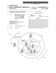
2.5 Interrupt Controller AY"chitecture
FigUJ.~e 2~6 g.ives a block d1agram of the 1nter'rupt controller used on the
Serie,'3 II Z··80
Interrupt requests are captured by the interrupt request
register (IRR) where noise spikes are filtered out and the interrupt
requests are latchec,L
requests that are not masked by tbe interrupt
rJask regJ.ster (H1H) are passed to the priori
control cireul
where
0
SERIES II 2-80 CPU
wIll cause a group interrupt to be genera ted. Uhen the processor accepts
the interrupt ~ .it Issues an interrupt acknowledge signal which causes (1)
the priority of all pending interrupt requests to be resolved. and (2) the
byte from the vector response memory associated. 11ll th the highest priority
request to be asserted on the proces~oris data bus. The Z-80 processor useS
this response vector as a pointer to a table of service routine addresses,
fetches the appropriate address from the table, and executes a subrolLtine
call to that address.
fiGURE 2-6
INTERRUPT CONTROLLER BLOO( DIAGRAM
-
[;MODE
[~~
R~GISrl:R
REGISTER
{
_.
.
,.
J.
f-
I
~~IS;~_-
STATUS]
~
11'
BUS
""
7-
:<
B'~~
.~
~
[ AUTO CLEAR
REGISTER
'Ij
INTERRUPT INTF..RRUPT
CONTROL
AO<
Ii
~
~
I
"
,
~
i'
I ! IN-SERVi~
r R:~::l
REGISTER
'"
ih
~
2>
l
A
--
PRIORITY CONTROL
.'"
AJ
'-~
4
.1\ ~
,
~ l?
ill
I
VECTOR
RESPONSE
MEMORY
GROUP INTERRUPT
-r---"-
-
INTERRUPT INTERRUPT
AREQUEST
REGISTER REQUESTS
.~
..
.
.
I
Other interrupt management functions are controlled by the Auto Clear
register, the interrupt service register, and the mode register. All setup
and programming of the interrupt controller is exercised through the
command register, and the internal state of the .controller is available in
the status register.
2.6 Interrupt Controller Operating Options
The interrupt controller I s mode register is used to establish the basic
operating conditions and options for constructing an interrupt driven
system.
SERIES I1.Z-80 CPU
- 20 -
Fixed or Rotating Priorities
1~.1t 110
in thE: r~orje re Bter .spec5.fJ.e.s T.lfJether tr10 interrupt cODtrol1er
operates in the fixed priority mode or in the rotating priority mode. The
fixed prlority mode (MO=O) assigns the
interrupt request inputs the
priority they are assigned on the S,,·, 100 blls that is, the VI 7 line is the
highest priority interrupt 1n the system and the VI 0 line 1s the leac'Jt
significant ilfterrupt In the system. This 1,s sho'l-JD in F,igm'e 2-"'/"
FIGURE 2-1
@--@---@--(~}--~(~'-@'--'--'0-~-~)
tOWEST
!·'iH-iHt.::i'
fiXED
MIVI
PRIORITY
PRIORITY
MODE
II\1TERRUPT
PRIOR!TY
MODES
ROTATiNG
PRIORITY
MODE
The fixed priority mode is the one most often used. although there exists a
possibility that low priority interrupts may never be serviced in a heavily
loaded system.
The indivj.dual masking feature~ however! may be used to
modify the effecti.ve priorHy str'ucture of the interrupt controller to
guarantee service to all peripherals.
In th~ fixed priority mode interrupts are normally masked such that only an
interrupt of a priority higher than the interrupt being servioed may
generate a new group interrupt to the processor. With the Series II Z-80,
each interrupt may be specified to erect such a masking "fence" or not to,
by setting the oorresponding bit in the Auto Clear register 9 al1ol"rir.lg a
great deal of flexibility in the effective system priorities of each
interrupting device.
If the eight interrupts have similar prior1ty and bandwidth requirements,
one effective solution is to select the rotating priority option (NO:1). As
shown in the· figure l the relative priorities tn the system Y'emain. the same,
except that the ohain 1s closed into a circle. In rotating priority mode
however p the lO1"iBst priori
poai Lion is assigned by hardware to t;he last
interrupt se~'viced.
This rotaUng priori.ty scheme prevents any s1
e
interrupt from dominating the systemc
It assures that any inter'rupt will
SERIES r I
Z~>80
CPU
not have to 111!"ait more than seven lnterrupt oycles before be.ing servioed.
Note that th~~re 1.s no nesting of interrupt,?} in the rotating mode; aLL
pending interrupts are masked from the processor while an interrupt is being
serviced.
Common and Indiv.:Ldual Vectoring
Bit M1 in the mode register specifies whether the individual interrupts will
branch to different lOCations upon i.:"l,ceeptance of an interrupt I Ol~ whether
all interrupts wtl! branch to the 1:HUlle lOCEit:lon.
the eOlIunon vectorlng
mode~
the response associated
th IREQO (VI 7 'w:Ul be asserted upon
interl~upt
aekno"Tledge~
regardless
of
y,rhieh
interrupt
is
being
acknowledged,
The common vectoring mode j.s useful if aU service routines
save the total machine sta te bef"ore entering the actual device service
routine, In such a case~ the processor branches to the common register save
routine, . then polls the interrupt controller to discover the highest
priority interrupt pending.
and branches to the appropriate service
procedure.
This approach avoids duplication of the register save routine,
Bi,t M1::::0 selects the individ.ual vectOl~j,ng mode 'irJhHe ~1"1;;;: 1 selects common
vectoring.
Polled Node
Bit 2 of the mode l~egister allmllTs the system to d1sable the group interrupt
output from the interrupt oontroller.
In the polled mode the processor may
read the status register in the interrupt controller to see if any
interrupt requests are pending. and which request has the highest priority.
Interrupt request bits may be cleared by software.
The polled Qode option
then bypasses the hal.. . dHare interrupt. the vectoring and fencing functions of
the interrupt controller while the request latching p masking, and priority
resolution remain unaffected.
Bit H2::::0 selects the interrupt L1ode~ H2:::1
selects the polled mode.
Haster Bask
Bit 7 of the mode register specifies the status of the caster mask bit of
the interrupt controller,
When the master mask bit j.s set, (1'17::::0) the
controller is disarmed just a,s if all the mask blts in the mask register had
been set.
lrJhen hit 7 is a 1 ~ thE:) chip is artJed and any unmasked actj,ve
requests will cause an interrupt output.
The remaining bits of the mode register specify (1) the polarity of the
group interrupt output~. which is always aetive lOIN on the Sel~ies II Z-·80
(1'-13::::0); (2) the polal~ity of the interrupt request signaJ.s~ '\,lh1ch is alHays
active low in S-·100 systems (M4=O); and (3) the register pre-selection
address.
These bits select whioh of the internal registers will be rea.d by
SERIES II Z-80 CPU
the prooessor during a data read
of the data transfer to and froJJJ
section.
A Su.ITlElary
contrallEn'.
controller is g.iven .in a .later'
['com the
the
Status Registe,r
The Status 1"'egister descrJbes
the lntel"nal state of
controller I as sur.m:narlzf.'d. i . n T h e
bits of the sta t.U[3
reflect the opera
described above, and indicate the
priority unmasked int
that is
Status bits SO-S2 oontain the
cOl1J.plement of the b;,irlar:v' vector"
the
st
in.ter'ru
pending.
The field should be cons:\.dered in,valid u.n1e38 the status btt
(the group interl"'upt bit) :U, set ( ::.:1)? indioating that at least one of
the interrupt request bits is set and unmasked. Status bit
indicates the
condition of the master mask in the Mode register. S3 equals 0 indicates
that the chip is disaJt'l.nedr.
33 equals
'p,
ar1J1ed~
ir1dieates th.e chip 1.3
t
indicates whether the oontroller is in interx'upt mode or polled mode, and
bi t S5 lndicates \Mhether' tbe priori
resolution is i.n fixed or rota
mode. Fj_nally~ bit 36 .is not used in this implementation.
F!GlilRE 2-ftl,
~ ~~;.rA~"'i!lll,;""T""Il.""~;,G;;""'=1MOm1=;"",_,,,,,,,,,,,,,,,,,~",,,,,,",,,,,,,,,,~_,_,,,_,,,,,,,,,,,,,,,m~,~~:'~~~,,=---;::;-...;T.~~...~"_~.--:.:="":l~:l<.:~~~
-
ll,,"'T;;Tl~0 ~~~l
-1 ,-":;3
1
'
il
".
L
f
!l
~
i~1I"Jh.nlV '/[CV(lIiJ WJDiC~\1iIB!'1i
rMUl~~1r.~i
~(O[l[
1111lC
M n~'t! HHlP"l@::nrf ~H'MVrf\f
I>MMASIl[,1' an 'HMl' ~~ o\lCi' n~ 11'U'l,
I!I
I
VlliUD !l)NU1' \iM1£fM @'JI'n@
n
C~-;l!fl
I ,;.oMMOl' VH.'"/ ()If,
AB'IMW
1-
I I"OLL[O
~··_--....---l.aM1:
I ACli,f/: HIGM
rW·f.f\'TH\~Q
----Ul.£lJJ POI..ARI1''If
@ ACWIE lAW
INPtfi
~
@ ~~If" DIS-!\!lL[!l
I
eN11" [N,lIIilI..!D
mil
/Jor
Il'/llil
~ @ ~NIT.P.AtJ1lO1·
PtEoour:r
~fJ.f:lS1Ud
1....-·_.._-..- . - _..-~-_ ..·_.--.MAlSl1EfI 1<'..$1( IlIO
tollQIX£ ~I$'l"[M
is
1
:,' .,'
I I ,\lITO Ct.f.J\1l 1'liJ);1:r00l
leI!! flJ£1j'
The Status register
controller's control
il'HGH
G'fI[S[U,:C:lflO1ll
Iftrr£fIHlo'Pi 5lD1hflOf ~t:,\UjTff~~
gil INI!:.,flVi"f f"Wi¥. Iq€GiS11W!
1l!ll :;[1
lU,ST ~
UNM£SMf.~
t1.C1~V[
~(?!
- - - - · - - - - - - - -.. I';Il\l\i,fill IIH[flfllJl"I·
II 110 IJWMJ\!"'1EJTh
(;J
P'OI.M'lln
!l ACHv( !JJW
<1~[1l
.---·--·--·-----<!!MflI.1C
&~OD[
@ INffl'llh.lN
----~--~Il:mln MODi:
l
·,NIEI'IF%Jn
MOO'lE
D l"Ol!\[!l
~
~,n.cC'10'l
I1i II~IIIO'"""" V[CTM
III 1i\l1[1I'I(~1j6"'F
!l\
jj()1'AYI~«,
L _ _ 'l,CI'O~
"--MAmr~ IMU,i\ £\II¥
iii ~,~ ilISMM[!lJ
~-'--.---lloIn~~\li"7r
~II\HI
/iI)
CHIP !lISllf'lMf.D
I.
CHIP AfIl'&tT,
read direct
executing a read
it does not require any preselection.
SERIES II
from
the
CPU
Interrupt Service Register (ISH)
The ISH is eight bits leng and is used to st~re the acknowledge status of
the interl~upt requests.. lr1hen an inter'loupt is acknowledged, the controller
clears the associated l"equest bit and. sets the eorresp<md.ing bit in the
ISH.
When the ISH bit is pr'ogrammed for' automatic clearj.ng~ t.he ISR bit
will be cleared before the end of the aclmoHledge sequence.
If i t is not
set for auto-cll~cn'~ the ISB hit must be cleared by command from the Z=·80
0
Internally, the controller uses the ISH to erect a "masking fence n • When an
ISR bit is set and the fixed priority mode is selected, only an interrupt of
higher' priority than the one being r.~1erviced "llil cause a J:1eltl interrupt
output, nesttng the lnterrupt irout:ines, and moving the masking fence up to
the new leveL
NejA! interrupt requests of' a priority lower' than t,he one
being serviced will be masked untn thE) ISH i8 cleared
the Z-80. When
the Auto Clear is specified. no masking fence is erected, since the ISH bit
is cleared during the ackno'loJledge sequence. The Auto-Clear funotion may be
. specified for each interrupt individually. by setttng the ,s,ssociated bit in
the Auto Clear register (ACR).
Information Transfers
There are two input/output ports associated with the interrupt controller -a control port and a data port. A read operation executed from the control
port will always read the status register, and a write to the control port
Hill ahlays 'loIl:"ite into the cmnmand register.
IIhen a read or wri.te is
executed. to the da.ta port~ l:lO"ilTever» the j.nfoI'Y.nation transfered depends on
which of the internal registers has been pre-selected by the preceding
command.
During read operations» the Interrupt Request Register (IBR), the
Interrupt Serv.ice Register (ISH). the Interrupt Mask Register (IMR), or the
Auto Clear Register (ACR) are pre-selected for reading by the bits N5 and
M6 of the mode Register.
For writing into these registers, specific
. commands must be issued to the controller; the 1-15 a.nd 116 bits do not
preselect registers for writing.
2.7 Commands to the Interrupt Controller
The interrupt controller!s command set allows the Z~80 processor to select
and alter all the operating modes desoribed 'above, to customize the
controller for (lif'fere,nt applications,
Coruma.nds are entered into the
command register by writing to the control pm-"/::.. In the cor.:u:nands described
below» lix,g indicates a IRdon! t care" btt position,
SERIES II Z-80 CPU
RESET
o a
The
reset conmand est;'";:,bli.shes a
000 000
:internal condition in the int"""',r'iU"II'".
kXlO:;W
controller~
~,
Fixed
prlor:U,;y [I
indivldual
veetol~B~
interrupt (non-polled)
ope.ration~ interrupt i
s and Ow
In the active low sense (normal) ~ ISH
preselected for
w (:hip dj"sar'ID,"~d by master lilask.
110de
1MR
= all
= all
ones, all requests are masked.
zeros, no auto clear B
ISH and IBH are cleared of all old requests.
ACR
CLEAR IBR AND Itm'
Coding~
000 1 0 X X X
hits in the Inten'upt Request Register and the Hask
cleared, no interrupts pending, no interrupts masked.
All
Registel~
are
CLEAR SINGLE 1MB AND rEB BIT
Coding:
0 0 0 1 1 B2 Bl BO
nrn and the
single bIt i.::; cleared in the
three bit field B2-BO where~
fA.
IRR,
The bit is specified
B2
Bl
BO
BIT SPECIFIED
()
0
0
0
0
0
1
1
1
0
0 ( LSB)
1
2
1.
0
"I
0
1
1
0
1
by "the
3
4
r,"
.)
6
or (HSB)
0
1
CLEAR 1MB
o OJ
bits in the IHE are cleared to
unmasked.
All
0 (]
xX x
zeros~
- 25 -
thus all interrupt requests are
SERrR~~
TT 7_Afl
0ml
CLEAR SINGLE 1MB BIT
Codlng~
A single
82-BO.
b.a
o0
1 0 1 B2 B1
ao
:l.n the mask reglster :is cleared p
as speci.f:ied :in the field
SET 1MB
Cod.ing~
00 1
~\
OXXX
All bits in the mask register are set to ones. thus masking all interrupt
requests.
SET SINGLE
nm
BIT
Coding~
o0
'! 1 1 82 81 80
A single mask bit is set. corresponding to the bit specified in the three
bit field.
The corresponding
is then masked out of the priority
resolution circuitry.
CLEAR IHR
Coding:
O'iOOOXXX
All bits in the request register are cleared to zeros. New transitions on
the .interrupt inputs 1J>l.ill be necessary to cause" an interrupt.
CLEAR ,sINGLE IRR BIT
Coding~
o
1 0 0 1 82 B1 BO
A single request bit is cleared to zero, specified by 82-BO.
SET IRR
Coding:
010'10XXX
All the request bits are set
interrupt output. Useful in te
to ones,
any tU1masked
bit ,,,il1 cause
an
SET SINGLE IRR 8IT
o
Coding:
A single
request
bit 1s set,
1 01 1 B2 81 BO
corl~esponding
to the bit specified by 82-BO"
CLEAR ISH
Coding~
01110XXX
All Service register bits are oleared to zero, fencing is eliminated.
SERIES II Z-81J CPU
CLEAR HIGHEST PRIORITY ISR BIT
Coding~
0 1 lOX X X X
The highest priority bit in the servioe register 1s cleared. Caution should
be exercised In us:lng 'this command if the auto clear option is specifJed!
since the bit cleared by this command may not be the bit intended.
CLEAR SINGLE ISR BIT
Coding~
The bit specified
o
five
low
all
B2 B1 BO
'fHROUGH
o
Coding~
contl~o13
1;
B2-BO is cleared in the service register.
LOAD HODE BITS
The
1 1 1
0
H2 Hl iVlO
This command
order bi,ts of the mode register are loaded.
options
except
the
Haster I1ask and read
operating
preseleotion.
CONTROL HODE BITS H5 p1'16 ~r17
Coding:
1 0 1 0 H6 H5 N1 NO
The field in the command 18 loaded into the regj_ster preselect bits in the
mode register.
The Nl ~ NO field in the command controls the master mask as
follows~
N'l
NO
0
0
0
NO CHANGE TO 1-17
1
SET
1
1
0
1
CLEAR N7
( ill(~gal)
PRESELECT IHR FOR IflUTE
Coding:
1 0 1 1 X X X X
The next write to the controller I s data port will load the mask register"
Various read opera.tions may be inserted betlrleen this coI'Il.tJ.and an,d the irlri te
operation.
PRESELECT ACR FOR WRITE
Coding~
1 1 0 0 X X X X
The auto olear register will be loaded on the next write to the data port.
PRESELECT :RESPOnSE l'-mHORY FOR WRITE
Coding:
1 1 1
a
0 L2 L1 LO
The vector response memory is preselected for writing. the byte which will
serve as B pointer to the Z-BO's ~ervice jump table will be loaded on the
next write to the data port into the level specified by L2-LO where:
L2
Ll
10
1
1
1
o
1
1
1
o
o
o
o
o
o
1
1
o
o
BUS INTERRUPT (VI #)
VI
VI
VI
VI
VI
VI
VI
VI
1
1
o
1
o
1
o
0
1
2
3
4
5
6
'7
2.8 Using the Interrupt Controller
Before the IntE~rrupt Controller carl do useful 11:ork it must be ini tiali.zed
under control of the Z·-80 processor. Because of the many opeY'ating options
available with the interrupt controller~ the controller may be programmed
using many different approaches. .The folloWing is but one of these ways to
construct a basic initialization and service routine.
1)
2)
3)
4)
5)
6)
7)
8)
9)
Disable Processor interrupts
Reset the interrupt controller
Setup vector response memory
Load operating options into the mode register
Load the mask conditions into the IHR
Clear the IRR
Cleai the master mask
Set processor interrupt mode to mode 2 i and load the service jump
table.
Enable interrupts.
The follo1tling simple program uses the 2-80 interrupt Dode 2 i and is intended
to both serve as a test of the interrupt controller and an example program
for using the interrupt controller.
SERIES II
Z~80
CPU
- 28 -
HAJJDLE,nS
"
~
;; 'tHE
FOLLO~iJIl>JG
JrliOftflCIIIlJ:!;!.3
'1"0 'TlfVZ:
Sg,"'UF,~
VEGE,:SSA,RY PHClGRAl,)J"iIHG
OF VECTOHED
ON
p
~ nVD IV IDllftL
; CONTROL.
REGISTERS IN THE MAIN
; SAVE:D UPON E1Ml"FlJC T'O [IN
;UPON EXIT FROH
.nn"EHHUPT"
.1:,\ \\.)"1",1""",,11.»),\;:';'
~
THE ZCPU AHE
llND HESJ:,'O,HED
~
~ DE,FINITIONS
IOBjL'3l:'~
OEOH
ICON
I0Ji3ASKfl·1 ;
BASE:
AIJDHESS ON Z-·80 BOAHD
ID,A,'I'
(
AND
FOE ~rEST HOU'I'INE:
J'BST HOUTINE;
l?P
STK
1000H
HERE.
HESTH'l'
; ENTRY POI!\iTS
OH(;,
,H1P
,J1>iP
,)"NP
SE~T'UPO
HaDE::
POLL:
,JHP
SEHV:
SAVE:
<JFJP
,,:I I'll'
SAVEO
EXT';' ~
,JNP
E){]CTO
DB
;00
MODE
~,
DB
00
.INT NODE
8, POLLED HODE
PHIOlUTY $, POI.LED HODE
INTERRUPT IN THE
I
00
DATA?~~VIO
IOlJ~lIJLL
r:OHHESPONDIlifG INT: DA
AUTO CLEAR
ETC.
SEHI:E;S II
CPU
;TBE LOCATIONS OF THE INTERROPT SERVICE ROUTINES ARE STORED IN
;THE JUMP TABLE BELOW" ITAB. CARE MUST BE TAKEN ~JHEH ORGiING
;THE PROGRAM SUCH THAT ITAB NEVER OVERFLOWS A 256 BYTE BOUNDARY
; IN MEMORY" AND THAT ITAB BEGINS AT AN EVEIl llEHORY LOCATION.
NOW
DB
o
SET"
$/2
NOW*2
TEMP2
ORG
SET
SET
SET
IF
ORG
ENDIF
!TAB:
))t1f
TEHPO
TEHP1
D\<J
D1IJ
Dill
DW
DW
Dl~
DW
SERIES II 2-80 CPU
SO ITAB GOES
;AT RIGBT PLACE.
,PSEUDO~OPS
;=EV£N ADDRESS.
$+OEH
;LAST LOCATION OF TENTATIVE ITAB.
TEMPO&OFFOOH
;ISOLATE 2 MSBso
$&OFFOOH
;IF THEY'RE TIiE SAME~
TEMP1~TEHP2
;DON'T ASSEMBLE THIS CODE.
TEMP1
;OTHERWISE~
USE BOUNDARY
;FOR ORIGIN.
INTO
INT1
INT2
INT3
INT4
1NT5
INT6
INT7
;JMP LOCATION FOR VI 1 ROUTINE
CORRESPONDS TO LEVEL 0 AT
VECTORED INTERmlPT CONTROLLER
AND SO ON.
- 30 -
; SETUP SUBROUTINE:
THE SETUP
;LOADS THE OPERATING OPTIONS
SUIBHOUTINE INITIALIZES THE 9519 ~
IN THE VARIABLES~ LOADS
;THE RESPONSE HElMIOHY WITH VECTORS TO 'TIlE JU11P TABLE (ITAB) ~
AND
;SETS THE 2-80 TO INTERRUPT MODE 20
SETUPO: D1
; DISABLE JPHOCESSOR INTERRUPTS
;SE1'
PT ~~DE 2
H12
LXI
HOV
STA1
XRA
LDMEM:
H,ITAB
A~H
A
OUT
ICON
CALL
HODEO
HilI
HVI
B·,OEOll
C,B
MOV
OUT
MOV
OUT
INR
INR
INR
DCR
B
; COHHANDS
PRESELECT 11E~lORY LEVEL
;LEVEL COUNTER : : : 8
; A : : : PHESE:LECT NEXT LEVEL CONNAND
ICOJl.~
;PHESELECT NEXT LEVEL
A1,L
;.A ~: L011J PNTR TO ,JUHP TABLE
;IIJJUTE THIS MEHORY LEVEL
IDAT
JL
L
B
JNZ
LDHEM
HVr
OUT
HVr
OUT
NVr
OUT
A,
; ,:rm1,p TABLE PNTR : : : NEXT ENTRY
~ NE)(T LE'".EL,~
; DECna1:E:tJT LEVEL COUNTER
;DONE FILLING K-fBHORY?
nm
;CLE:AH
ICON
A~
OB
;CLEAR ISH
Ai OA9H
ICON
E1
RET
HODEO:
,HL
THE JUMP TABLE
; HIGH BYTE TO ACCUHULATOR.
;1 REGISTER
AINS HIGH ORDER PNTR
; 11.:;:0
i 11£S£'1' ') 9
;S£1 THE CONTROLLER OPERATING MODES
,CLEAR HASTER BASK PRESELECT IRR
; ENABLE PfiOCESSOR INTERRUPTS
;EXIT
LDA
MODES
, A~. ,". , •. " " ."-'.1'.'
ORI.
OUT
ICON
;HAKE INTO NODE SET COMNAND
;SET MODE
MVI
A»OBOH
OUT
ICON
HASKS
IDAT
;;HRITE THE t-:iASK
HVI
A 1 0C011
; A - AUTO CLEAR PRESELECT COMl\IAND
OUT
ICON
CLEARS
;; A
LDA
OUT
LDA.
OUT
RET
IDAT
; A := PH:l~SELECT £'1ASK COHHAND
;; PHESELE\;T THE !1ASK REGISTER FOR HRITE
; A. ~: !:'ll\.SK
ACH
.~
AUTO CLEAR PATTERN
ptoJk~ITE AUTO CLEAR REGISTER
;EXIT
"~
311
~"
SERIES II
Z~80
CPU
; HaDE 1 IS A SUBROUTINE WHICH CHANGES THE OPERATING HODES TO THE
;VALUES CONTAINED IN THE VARIABLES AND RBINITIALIZES THE
; CONTROLLER. IT IS TO BE USED DYNAHICALLYo CHANGE THE VALUES
;AT MODgs" NASKS, AND CLEARS AND CALL r,lODE. THIS WILL CHANGE
;1'HE OPERATING OPTIONS WITHOUT AFFECTTIl\lG rRR OR ISH"
,.
MODE1
~
D1
CALL
E1
MODED
;DISABLE INTERRUPTS
; SET ~10j)E:S
;ENABLE INTERRUPTS
;Exrr
RET
; THE FOLLOiHNG SUBROUTINES ARE USED IF THE POLLED HODE
;OF OPEHATION HAS BEEN SELECTED. A CALL TO POLL HILL RETURN
; THE CARRY BIT CLEAR IF AN INTERRUPT REQUEST IS PENDING.
; OTHERWISE THE CARRY WILL BE SET.
;A CALL TO SERV WILL SERVICE THE HIGHEST PRIORITY INTERRUPT
;THAT LS PENDING IN THE SYSTEM AND RETURN.
; POLL. USES A &: F
;SERV USES A»F,DE,HL
.
"
POLLO;
TN
ICON
;INPUT CONTROLLER STATUS BYTE
; PUT INTERRUPT PENDING FLAG IN CARRY
; EXIT
ICON
;INPUT STATUS BYTE
;r1ASK FOR LEVEL
fiLe
RET
SERVO~
IN
ANI
BLA
LXI
ADD
l-lOV
HOV
INX
MOV
XCHG
PCHI..,
SERIES II Z-80 CPU
01H
;OFFSET~LEVELlI\i2
l-l"ITflB
L
L»A
; HL POINT TO JUHP TABLE
;HL+OFFSET=VECTOR
; HL~~ VECTOR
E~H
l-l
D»H
;DE=ROUTIN~
ADDRESS
;HL::::DE
; JU)l.IP
TO SERVICE ROUTINE
- 32 -
;ROUTINES SAVE MID EXIT: THESE ROUTINES ARE INTERRUPT SERVICE
THE SAVE .ROUTINE SAVES THE MAIN REGISTER
;BANK IN THE PROCESSOR CHIP~ RE.E:NABLES DJTERRUPTS 9 AND RETURNS
;TO THE SERVICE ROUTINE" IT' NUST BE CALLED AT THE BEGINNING
; OF EVEHY SERVICE' ROUTINE _.~
;
START:
SAVE
;TBE EXIT ROiJTINE SIGNALS nm INTERRUPT CON'TROLLER nUT THE
;SERVICE ROUTINE IS FINISHED p HESTORES THE HACHINE STATE~ AND
! RETURNS TO TIlE INTERRUPTED PHOGRiU1 p OR: IN THE CASE OF POLLED
;OPERATION~ THE: CALLING PROGRAH,
EXIT SHOULD BE ENTERED BY A
;Jl1P INSTRUCTION p ~nTH THE LoEVEL OF THE INTERRUPT BEING
;SERVICED IN THE A REGISTER. SERVICE ROUTINES SHOULD BE
;STRUCTURED p THEN;
ST ART; CALL
SAVE
;SUPPORT ROUTINES"
(MAIN SERVICE ROUTINE)
.. 33 -
SERIES II Z-80 CPU
;TEST PROGRAM~ THESE TEST PROGRAMS USE THE ABOVE ROUTINES TO
;TEST THE OPERATION OF THE CONTROLLER IN.A SYSTEM. THE ROUTINES
;LIGHT A BIT ON THE PROGI(lUifo1ED OUTPUT PORT OF THE
;INTERSYSTEl:1S FRONT PANEL CORRESPONDING TO THE HOST RECENT
;INTERRUPT SERVICED. THE S~1
VI "7 LINE COHRESPONDS TO A
,LEVEL 0 INTERRUPT AT THE INTERRUp'r CONTROLLER, AND SHOULD
;LIGHT FHONT PANEL PORT LIGHT O. A SHIPLE TEST OF THE
; INTERRUPT SYSTEM IS TO RUN TEST AND GROUND EACH VI LINE IN
;TURN, CHECKING THE PROPER FRONT PANEL LIGHT.
JTHE TEST ROUTINES EXIT TO RESTRT 1tJHEN THE HOST SIGNIFICANT
;FRONT PANEL SWITCH IS SENSED LO\'Il. PLTSTO IS THE POLLED
;VERSION OF THE TEST ROUTINE WHICH OPERATES SI1"11LARLY.
;THE STATE OF THE NEXT~'l'O-MOSl'-SIGNIFICANT FRONT PANEL
; SWITCH DETERl'1INES WHICH ROUTINE RUNS -'- HIGH :;:; INTERRUPT TEST,
; l.OW :':: POLLED TEST.
TESTO~
HALT:
LXI
XRA
OUT
STA
CALL
IN
:liLC
,·HJC
HLC
Z~80
A
FI'
MODES
SETUP
FI'
RESTRT
,JNC
ltrL T
POLTST
,J~/1P
HALT
PLTSTO: LXI
IIT\lI
STA
CALL
XRA
OUT
1'1,TST1 : IN
RL'C
JNC
RLC
,JC
CALL
eNC
"HiP
SERIES II
SP!STK
CPU
SP!STK
1\1 4
HODES
SETUP
A
FP
FI?
f{ESTRT
TEST
POLL
SERif
PLTSTl
;SET STACK POINTER
; ACCUHULATOR GETS o.
; CLEAR FRONT PANEL LIGHTS
; INTERRUPTS AND FIXED PRIORITY.
; SETUP CONTROLLER.
;GET S\HTCHES.
;PUT D7 INTO CARRY,
; AND EXIT IF LOt;).
;PUT D6 INTO CARRY.
;DO OTHER TES1~ IF D6 IS LOH.
;HALT & WAIT FOR IlnERRUI'T
;CONTINUE FOREVER
;=FIXED
;1\
:=
PRIORITY~
POLLED HODE
o.
;BLANK LIGHTS"
,GET SW ITCliE~:L
,PUT D7 INTO CARHY.
;EXIT IF SVJITCH IS LOW. OTHERWISE,
;PUT D6 INTO CARRY.
;GO TO OTHER TEST IF SHITCH IS UP.
,CHECK IF ANYTHING N~itl •
;YES? GO DO IT.
;REPEAT,
; INTERRU PT SERVICE ROUTINES ~
INTO:
INT1:
CllLL
SAVE
;SAVE EllVIBOWlENT FIRST.
HVI
BVI
JHP
CALL
BVI
A p 01H
B~O
;.11. GETS LIGHT PATTERN
;B GETS LEVEL iff
;BRANCH TO CONHOH SERVICE ROUTINE
1-1"1
INT2:
INT3:
INT~:
1NT5:
INT6:
INT7:
INT:
JHP
CALL
MVI
MIT I
JHP
CALL
MVI
MVI
JHP
CALL
MV1
BVI
JHP
CALL
NV1
BVI
,JHP
CALL
HVI
HVI
JHP
CALL
INT
SAVE
A~02H
B w1
INT
SAVE
A 9 04H
Bp 2
INT
SAVE
A?08H
B9 3
INT
SAVE
Ap 10H
B~4
INT
SAVE
A p 20H
B,5
INT
SAVE
A,40H
B~6
INT
SAVE
!-lV1
Ap BOH,
MIT I
JHP
B,1
INT
OUT
FP
ApB
EXIT
HOV
JHP
END
;UPDATE LIGHTS
; A GETS LEVEL 11
; RESTORE ~,lACHIJ.IlE STATE
2.9 Series II
BUB
Interface
Thfl SelR"iee II Z~80 provides a numbel~ of' operaUng options lrlhich g.ive the
uJ!er
Borne
control over the procBssor-ta··buB :1.nterface 1 while still
aorrssponding to the IEEE bus . specification.
These options include
proceSsor Bpe~~d selection of 2 or 4 ~mz and optional ad.d! tion of a single
wait state to all instruction fetch cycles (the instruction fetch oyc~e of
the Z-BO processoI' is shorter than other memory cycles of the processor p and
represents the worst case for memory access timea). all memory cycles, Or
all I/O cyolEH:I.
In addition to these basic options a special feature has been included to
allowl the implementation of extremely h:Lgh rel.iability systems. In order to
meet the IEEE standard for S~100 bus devices using a Z-80 processor, all bus
address and status signals should be latched. This is because the z-80 chip
can change its effective address at the end of an instruction fetch cycle
while the bus read strobe is still valid. The IEEE specification oorreotly
P!~ohibits such timing ambiguities.
To comply with this specification the
Series II Z-BO includes hardware latches on all address and status lines to
the S-100 bus.
There are two modes of operation of these latches: Partial Latching and Full
Latching.
Th~= Full Latch mode is designed for extremel;'( high reliability
systems w or operaUon in electrically noisy environments.
The Full Latch
mode halves the number of signal transitions On the bus and restricts all
changes In address and status signals to specific, non-criUcal parts of
the bus cycle ~ thus drastically reducing btl.s noise and signal crosstalk.
The Full Latch mode decreases the effective merlOry access tiIJe of the
processor'j requiring that either very fast memory boards be used (160 nsee.
worst case board access for Ml cycles requires chip speed of approx.
125
nsee in a typical design), or that a single wait state be added to all Ml
cycles j slowing the processor approxim~tely 10'.
Other system parameters 1111111 usually reduce the vlai t state requirement to
insignifioance, but the occasional necessity for the faster Ml cycle can be
sattsfied with the Partial Latoh mode. This m'ode does not control signal
transitions as does the Full Latch mode p but provides for operation at 4 mHz
without wait states if proper cycle triggerring is employed.
All
InterSystems Series II memory boards 1,dl.l support no-walt operation at )-1
11Hz using the Part.ial La.tch mode.
SERIES II
Z~80
CPU
- 36 -
2010 Direct
~1emory
Access Opera 1:10ns
The last major feature of the Series II 2-80 concerns the relationship of
the processor to Direct Memory Access devices on the bus.
The !:E:EE bus speoificatiOl.1 defines a special protoool f'Or the transfer' of
bus oontrol from a permanent bus master, in this case your Series II 2-80,
to a' temporary bus master suob as a DNA device or attached peripheral
processor.
This protocol involves a specially timed and overlapped
transfer of the various signal groups on the bus such that the DNA devloe
and the CPU are both d1~iving the most cri.tical bus lines in given i.nacUve
states during the transfer operation.
The circuit which controls this Uming could be included on. el ther the
processor board or on the DMA board. It has been included on the Series II
2-80 board. for two reasons: Fj.rst~ if it is included on the processor
board.~ it need not be duplicated on every DHA board .in the system~ and
second$ sj.Dce no currently existing DBA boards include such. a c.ircuit~ :!.t
is much easier to modify an existing board to meet the S-·100 standard H
this circuit 1s centralized on the processor board.
The
the
to
may
and
Series II 2-80 board~ then" contains a circuit which will conduct all
timing of the bus transfer~ and tri·-state its own bus drivers according
the IEEE specifica.tion (sections 2.8.2.1 through 2.8.2,,4). m!A devices
sense the two bus transfer signa13~ XFER I and XFER II? on the SDSB line
the CDSB line respectively,
The 2-80 also includes pull-up R~esistors on the four DBA arbitration lines p
30 that they need not appear else~lhere in the system, and 10 ohm resistors
in series 'itlith the control output lines, to prevent dr:Lver fatigue a.nd
glitches during the overlapped bus transfer.
- 31 -
SERIES II 2-80 CPU
SERIES II 2-80 CPU
- 38 -
Sect.ion 3.0
Board Setup
3.1
Bus Interface Setup
Selecting the Processor Speed
Selecting the Latch Mode
Adding Single Wait States
Non-Maskable Interrupt Setup
Standard Bus Interface Configuration
3.2
The On-Board EEPROH and Automatic Bootstrap
EPROM Type Select
EPROM and Jump Address Selection
Enabling the EPROH and .Jump
EPROM Wait States for 4 mHz. Operation
InterSystems Standard EPRrn1 Configuration
3.3
Input/Output Port Setup
I/O Base Address Selection
3.4
Vectored Interrupt Controller Setup
Using an Off-Board Interrupt Controller
3.5
Memory Management Setup
Locating ·the Address Translator in Nain Hemory
Standard Hemory Nanagement Configuration
3.6
Front-Panelless Operation
Memory Mrrite Strobe Generation
Front-Panel Control Strobes
Front Panel Header in Front Panelless Systems
3.7
Summary of the Standard Setup
3.8
Jumper Summary
3.9
Installing the Board in Your System
- 39 ..
SERIES II Z-BO CPU
====..
11
I
0::
o
W
....J
O::....J
"'(§~
-1:011 Z
ttu0
0-
>
SERIES II Z-80 CPU
This section or the manual describes how to set up the Series II Z-80 for
operation in your system.
Ce!~tain jumpers on your board are only used in
aiSsembly or in testing'w and these will be described only in the
reference section.
Figure 3-1 shows the board location of the jtllIJpers we are concerned
this section.
~d th
in
3.1 Bus Interface Setup
The first and most important ohoice in the setup of the 2-80 board is the
selection of processor speed.
Either 2 HHz or )-\ HHz operation ma.y be
selected 'iJlfith the
jumper ,1G"
The choj.ce of processor speed is a
complicated decision iJr.l'\fOlvJ.ng the access times of the other boards in the
system~ the latch control mode selected w and the use of wait states o
Table 3-1 gives the various acoess times associated with the different types
or processor cycles at 2 ?J.Jd 4 t'1Hz l' for the full and partial la tchi.ng
modes,
Note also that the effecttve access time differs fOj:' static and
dynamic or edge.·triggered devices, This is because an edge-aotivated device
such as a dynamic memory must. Ha1t to begin its cycle untH certa:Ln
information is guaranteed to be valid, whEe static devices respond to
address changes as fast as possible. and do not require a strobe signal to
begin their cycle.
Table 3-1
Processor Access Times (in nsee.)
Cycle Type
2 NHz
')
c:
IIf/wait
)~
tHz
4 whrlaH
~---~~-~---~~~~-~--~-----~-~~~~~~~~-----~~~~~---~~-~
Nl Stat.
H1 Stat.
H2 Stat.
H2 Stato
H1 Dyn,
H1 Dyn,
X'J/2 Dyn.
Hc~ Dyn"
I/O F 01"
Platch
Flatch
Platch
Platab.
Platen
Flatcb.
P.latch
Flaten
Platch
280
220
530
1020
1280
1070
'1520
395
645
810
1310
310
560
580
220
1170
410
810
6l.j·O
1080
910
1310
1140
270
560
520
900
1 1100
).[00
650
780
410
160
310
lno
Hhelre ~
AIl tJm8s a.re j.n na.noseoonds, HI rE,fers to an instruction fetch
cycle" H2 refers to all other memory cycles, Platch refers to the partial
latching mode, and Flaten refers to tb.e full latch mode.
It sJ:lOuld be noted that these are board level access times, rather than
level aocess times. that is, no account has been taken of logic or buffer
SERIES I I Z,-tlO CPU
delays on the memory board but full worst case delays on the processor have
been included in the calculations.
It CBn be BeeD that the correct choice of bus cycle depends on a variety of
The most reliable bus cycle is the fully latched cycle. but access
timee Bra considerably Shorter, especially for H1 cycles which are already
l~hort in the Z=80.
It is therefore recommended that if the full latch wade
is used at 4 MHz; a wait state be added to all M1 cycles. This will slow
the operation of the processor approximately 10%. but. allows the use of 300
nsee.
static memory boards and 250 nsec. dynamic menory boards with ease.
Adding a wait state to all memory cycles and using, the full latch mode
allows the USl;; of less expensive ,1~50 nsee.
static or 1+00 nsee. dynamic
memory boards~ but slm~s the processor by 25%.
t~ctor~.
Full speed 4 HHz operation should' use 'the partial latch mode. HhHe this
mode creates somewhat mOl~e bus noise than the full latch mode~ it allows
the use of 250 nsee.
static memory boards~ and 200 nsec.
dynamic or
edge-activated memories without wait states.
(Note: The above calculations
for edge-activated and dynamic memory boards in the partial latch mode are
derived using the rising edge of the PSYNC signal as an address valid strobe
to start the tlemory cycle, aborting the cycle later if it is an I/O cycle.
In the full latch mode the start cycle trigger is the IEEE address and
status strobe. STVAL.)
Selecting the Processor Speed
Pin-jumper JG selects the processor speed.
of the board between U5 and U10.
It is located on the right side
Processor Speed, JG
2 HHz.
4 NHz.
B to C
A to B
Selecting the Latch Mode
The latch mode of the processor is selected at pin-Jumper JH-1, located on
the right side of the board between U12 and U13.
Latch
Mode~
Full latch
Partial latch
SERIES II Z-80 CPU
JH-l
B to C
A to B
Adding Single Wait States
A single wai t state may be added to any instruction fetch. any l11emo!'y
(lncluding lnstruction fetch cycles). any 1/0 cycle, and any referen(:~e to
the on-board EPROM.
'The addition of these wait states is controlled by
pin~juxllpel~s ,JH-2 through ,JH-5. also located betv,reen U12 and U13,
It should
be noted that~ for 4 MHz operation 9 all standcu'd EPHOI1 cO:cJponents urill
require a wait state for correct operation.
Wait State Selection.
Cyole Type
,,Jumper
JH-2 thru JH-5
1 waH
no-wait
----~~~~~~~~--~-------~-~---~~-~-~~~~-~-~
I'll
,JH·-2
,JH-3
All Hemory
JH-!'!
All I/O
On-board EPROM ,JH-5
A
fA
A
A
to B
to B
to B
to B
B to C
B to C
B to C
B to C
Non-Maskable Interrupt Setup
The last setup we are ooncerned wHh in the bus interface section is the
connection of the non-maskable interrupt line. This line, as yet unused in
most 3-100 systems, may be conneoted to either the 111'11 line on the S-,100
bus, Or to the Power Fail Pending line, or disconnected from the system.
If you are uslng a Pot·,rer Fail anticipation c j.rcuH, and support the cirouit
with software routines that respond to an NI:-11 as a power fail p then connect
1IT1I to Power Fail.
If you have some other use' for the Non-Maskable Interrupt, then it should be
Connected to its Oim pin on the bus.
If you do not use the line in your
system p disconnect the NfI-U line from the bus entirely by removing the shunt
from the IN pin-jumper.
Non-Maskable Interrupt, IN
mlI to NM1
NMI to Power Fail
No NHI to Bus
A to B
B to C
OPEN
SERIES II 2-80 CPU
InterSystems Standard Bus Interface Configuration
Figure 3-2
Sh0101S
the standard configuration for
board 1s shipped from
following options:
~
*
*
~
the
faotory.
This
the
bus interface as the
oonfiguration represents the
4 ~Hz operation
Full latch mode
Single wait for M1 and on-board
NMI connected to NMI
EPRa4
Note that whil<:l the wait for the on-board EPROH is enabled? a wait state
w:lll not be added to the cycle until the EPROH is enabled with the EPROH
enable jumper~ to be described later.
fIGURE ,1-;::
STANOIIRO (jUS
INTE!1f~
_
8.
l-ao
SERIES IIZ-80 CPU
3.2 The On-Board EPRON and Autowa tic Bootstrap
The on--board EPRON Bocke t may be oonfigured to accept any of the t'ollm·,ini
standard parts~ or ;,:my compatible parts;
EPROH TYPES
Hanufacturer
Intel
Part ff
Size
2'708
2'758
2'716
1 K
1 K
2 K
)4 K
27
Addressed at
1 K boundary
1 K
2 K
1! K
The on-board EPRON and the reset jump functions are addressed at the SBJ118
location in memory ~ which may be at any 1. 2, or 1.* K boundary (depending on
jumper set-up) in the 64k primary address space.
lIlhen a EPRON is in the
system and enabled. and the Reset jump is enabled? a reset to the computer
system will be acoompanied by a jump to the first byte of the on··board
EPRON. This operation is referred to as the l1auto-bootstrapil, If the EFRON
is disabled and the Reset Jump is enabled. the processo~ will jump to the
location in main memory that is set at the EPROl·l address jumpers,
EPROM Type Select
The follOWing table gives the settings for the EPROM type and size jl~pers.
Jumpers JA and JB are in the upper left hand corner of the board, and JE is
in the up-center region. The "NONE" row gives the proper settings for using
the Reset Jump funotion t,rithout. usj.ng the on-board EPROH.
The i'STANDARDiV
row gives the settings for using the InterSystems ' 2708 bootstrap EPROM at
address FOOD hex,
-
J.j5
-
SERIES II Z-80 CPU
EPRm1 Type Select ,Jumpers
TYPE
,JB-5
JA-2
,J A···'
,JB-6
JE-l
JE-2
---~~.~-~~-~-~-~=~~~~~~--~-~~-~~~~--~-~----------------
2708
2758
2716
2732
AB
AB
AB
';Ii
*
A
A
AB
B
'*
"*
Me
AB
Be
Be
c
Be
Be
Be
BC
(NO EPROl'1, J'UMP TO ANY 1 Ie BOUNDARY)
NONE
lIB
STANDARD AB
i
AB
*
(STANDARD=. 2708 AT FOOD
AB
BC
Be
\lhere fII*n indj.eates that
for this EPROM type.
the
jump~r
B
B
c
C
C
A
A
HEX)
participates in the address selection
EPROH and Jump Addl"ess Selection
Once the EPROH type has been selected 9 j.t may be addressed in the 64 K
primary address space of the processor using the jumpers at JB that lliere
not previously assigned in type selecti.on, The Ju.mp and EPROH are addressed
by defining a matching address for the starting loce.tion with jllIJpers JB.
Connecting A to B will match a lione ll on the corresponding address bit, and
connecting 13 to C will match a "zero n •
The standard location for
InterSystems bootstrap EPROHs is FOOO heJL
The Std.
column gives the
jt~per settings for use with the standard boot EPROM.
EPROH and ,Jump Addressing
,Juraper
Address Bit
"0 ne "
"Zerol!
Std.
-~~~-~~~-~-~------~~~--~-~~~~--------~~~---~~
,JB-·l
A 15
AB
Be
,JB-2
,JB-3
A
11~
1\.B
1\.13
Be
Be
Be
BC
BC
,JB··4
,JB-5*
,JB-6~H'r
A 13
1\. 12
A. n
A 10
AB
1\...'3
AB
1\.13
AB
1\.13
AB
Be
Be
*' Not used in the addressing of 2732 EPROUs .
•• Not used in the addressing of 2732 or 2716 EPRals.
SERIES II 2-80 CPU
-
lj·6 .-
Enabling the EPROH and ,Jump
Onoe the EPRON type and addreSB have been selected. tIle EPROH may be enabled
by appropriate connection of the EPROM enable jumper ,JJ-1, located on the
right aide of the board between U 24 and U 25.
I f you do not wish to use
the on-boal.~d EPROM~ or 1f you w:lsh to use the Reset jump without the
on-board EPROM~ JJ-1 should be used to disable the EPROM.
The Reset jump is enabled ldtb jumper JK? located on the right side of the
board just below U 25.
The following table gives the different
associated with the settings of these jumpers.
EPROH and Jump Enables
Funct:Lon
No EPROM, No Jump
EPROM enabled ~ No ,Jump
JJ·-·l
AB
AB
AD
BC
BC
Auto-Boot
(EPROM and Jump enabled)
Jump to Off-board memory
BC
EPROM Wait States for 4 MHz Operation
It should be noted again that for 4 l~H.Z operation all currently avaHable
EPROH's of the 2708 fam:Lly us(~d on the Series I I 2-80 will require a ii/aft
sta te added to any memory cycle \1h].oh references the EFRON. A pin-·jumper
to add a wait state to EPROH cycles only has been described above. I f th1s
jumper~ JH~5 ~ 1s connected. frow A to E, and the EPROM is enabled, a single
wait state will b·e added to all references to the EFRON.
InterSystems Standard EPRor·j Configura. tlon
The
standar'd configuration for the jLUllpers associated iorith the EPRml are
This configuration of jUrJpers represents the following
shotm in FiGure 3··30
options:
*
2708 EPRON type.
'" EPROll address is FOOO hex, location of InterSystems
*
bootstrap.
EPROM disabled.
• Reset jump disabled.
• Single wait state added to EPROM cycles.
use the EPROH 9 simply insert your FOOO InterSystems Boot EPROl"!
position U 21 ~ and enable the EPROM by connecting JJ-1 from A to B.
To
at
A
SERIES II 2-80 CPU
single wait state will be added to EPROn cycles once the EPRON is
ana.bled. (The EPROM wait sta te should be disabled for 2 rIHZ opera.tion).
If' you wish to use the Auto-Boot feature 1 whereby a ,jump to the Bootstra.p
program is executed upon Reset~ connect jUDper .JK from B to C-
3.3 Input/Output Port Setup
Four I/O ports are used on the Series II Z-80 board; they may be addressed
at any four-port boundary within the 256 possible system I/O ports. These
I/O ports are used to set up and control the Vectored Interrupt Controller
and to load the relocation registers of the memory management system.
The base address of the on"·board I/O ports~ called BASE, is selected with
pin-jumpers .JD-1i throue:;;h JD-6! located bebJeen U 2 and. U 3. The on-board
I/O ports are assigned the following functions:
SERIES II Z-80
CPU
- 48 -
Ta,ble 3··3
I/O Port Functions
Function
IN
[lASE
Read VI Controller Data Port (reads
OUT BJ\..SE
BASE+l
BASE+1.
Write to VI Controller Data Port
Read VI Controller Status Port
Write to VI Controller Control Port
BASE+2
BASK+-2
(not assigned)
Write to Page 0 Relocation Register
Pre-selected VI register)
IN
OUT
IN
OUT
IN BASE+3
OUT BASE+3
lAT~rite to
(not assigned)
Page 1 Relocation RegisteX'
I/O Base Address Selection
Tbe I/O base
significant
between tl1e
address are
settings for
address is selected by defining a matcbing address for the most
6 bits of the processors g I/O address,
The correspondence
various S8 t tings of the JD jurn.pers and the processor I/O
given in the following table.
The "Std. flU coluEln gives the
tbe InterSystems' standard I/O base address p EO hex.
LID Port Selection, JD
Jumper
JD-1
,JD-2
JD-3
JD-4
JD-5
JD-6
Address BH
A 7
A 6
AS
A 4
A 3
A 2
"lero"
"Cne"
Be
AB
BC
BC
BC
Be
Be
AB
.AB
AB
AB
AB
Std. (EO)
AB
AB
'Be
Be
illustrates the jumper ~ettings for the standard I/O base
address of EO.
InterSystems software will use this configuration. and we
strongly recommend that unless a specific conflict develops~ you use the
standar>d configuratiol1 p as softMare exchange ~lill be greatly facilitated.
Figure
3-4
- }.J9 -
SERIES II l-80 CPU
Port assignments for the standard configuration are;
EO _ VI Data Port
El = VI Control/Status Port
E2 - Page 0 Relocation Register
E3 = Page 1 Relocation Register
3.4 Vectored Interrupt Controller Setup
Once
the
base address has been selected? the Vectored Interrupt
may be enabled.
The enable for the controller is jUIJper JJ~2~
located between U 24 and U 25 on the right side of the board.
110
Contl~ol1er
VI Controller Master Enable
JJ-2
,JJ-2
VI Enabled
VI Disabled
Using an Off·-Board Int.errupt Controller
The board may be configured suoh that the on-board interrupt controller is
bypassed and the 2-80 processor responds to the group interrupt and issues
interrupt acknmdedge cycles to the 3-100 bus.
The vectored interrupt
controller must be removed from the board, and jumpers JF and JI should be
adjusted.
should be
JF is in
right side
(Caution: the 95'19 Controller Ie is a. static-sensitive chip, and
stored in anti-static foam, or wrapped in a.lUt:linUlll foiL) Jumper
the center' of the board next to the 2-80 chip, and JI is on the
of the board, between U 11 and U 23.
SERIES II Z-80 CPD
Bus Interrupt Enables
Function
Local
Controller
Into Accept
Bus Int, Assert
BUB
Conventional
Interrupts
11 to C
fA to B
B to G
A to B
If these jumpers are not installed, or if they are connected from B to C,
they enable the
vectored-interrupt controller circuitry.
3.5 Nemo.ry Managem1:,mt· Setup
A number of options
(1) Eitber a single 4
pages may be selected.
in main memory.
(:3)
disabled with a master
exist in the setup of the address translator:
K relocatIon page or 2 independant 11 K relocation
(2) The relocation lIirlindow" may be located anywhere
The EH1tlre address translator may be enabled or
enable jwoper.
The following table gives the settings for the number of pages and the
master enable jumper. The InterSystems standard configuration is to enable
both !.j K pages.
Address Translator Size and Enable
Function
,JC-5
JC-6
Single 11·[ pagE)
THO i.j.I{ p"lges
AB
BC
Be
Be
Translator Disabled
X
X
AB
iff:
Be
lilhel"e iH{;Vf indicates that th1s jw:n];')er' participates in the address decoding 9
and "X n indioates a "don't care" setting.
Looating the Address Translator in Main Memory
Once the size of the translation window has been selected, it may be lOCated
in main memory on any Ii K boundary if the window size is 4 Ie, or on any 8 K
boundary if both ij K pages have been enabled. If the translator has been
disabled
the master enable jtUDpex', JC,-6 1 the setting of these adclre,ss
jumpers is insignificant.
The translator is addressed by defining a match address for the first byte
of the window area with JC-1 through JC-~. The following table gives the
SERIES II
CPU
6orrespondence between address bits and the jumper settings, as well as the
InterSystems standard location for thl:" address translat.ion 'i<lrindow" AOOO
hex.
Address Translator Addressing
Jumper
Addre:;:H~
J'e,", »
A 15
JC-2
A III
A 13
A '12
JC-3
JC-4*
Bit
"Gns uu
~!Zeroml
Std"
AB
Be
AB
AB
Be
Be
~ NOTE: The J'e'"·lI jumper is only used in the address decoding if a single }-i K
page has been enabled.
If both translation pages a.re enabled~ ,JC-1.I is
always connected B to C.
InterSystems Standard Hemorjl' f1anagement Configuration
The board is sb.ipped fk'orn the faetory 1i1T1 ttl the
*
fo11o~.oJing
options selected:
Base Address is AOOO hex.
• 2 pages seleoted. but the unit is disabled.
To use the unit in the standard
()onfigul'a tion,
siDlply enable the
unj,t by conneoting JC·_·6 from B to
C.
The enabled configuration is
shown j.D Figure 3-5.
j'leDory from
AOOa to klFFF will be relocated as
Page 0, and memory from BODO to BFFF
t,ri11 be relocated as Page 1. Note
that once the memory L2anageDent unit
is enabled. it must be initialized
fOJ:' proper opera tioD., inasmuch as it
t'll1J. coos up at reset l1lith both
registers referencing OO,OOOOH
the bottom 4 K of wain memory.
SERIES II 2-80 CPU
The Serles II Board s.upports f1l'ont-panelless operation Tilri th a number of'
jumper seleotable features. These include:
*
H\\1RT Hemmoy Write Strobe Generation for all bus
dev.tces.
• Front-Panel Control Strobes, Data In Disable and
Sense Switoh Disable disconnect from the bus.
~
Reset, Jump Enable, and Ground available at a 20 pin
DIP header for simple controloonnections.
Memory Write Strobe Generation
The generation of the Hemory Write Strobe., HhmT, has traditiona11y bE)8n the
function of front panel devices in S~·100 systems~ where it is implemented as
prooessor memory Tt.rrite OR front-,panel deposito
In a front-panelless system the generation of the merJory .write strobe
beoomes the respons.ibility of the twocessor.
The prooessor must generate
the MWRT signal not only for' its own cycles, bu.t also for any Dil~ect l-lemoK'y
Aocess Device that may have temporary control of the system bus. A circuit
to perform this function is included on the Series II processor board~ and
may be ena.bled. for use in fr'ont-panelless systems !!lith pin-jumper JO.
strobe generation mu~t be disabled in front panel systems to prevent
conflict with the front panels' generation of the strobe.
tfWRT Generation, JO
l1t'l1RT enabled
HllmT disabled
The
Sel~les
II board is shipped w.ith the t\HRT strobe disabled.
Front-Panel Control Strobes
The front panel data control strobes should be disconneoted when the board
is used 1n front-panel1ess systems to avoid possible conflicts and noise.
These
lines
have
been
inoluded
1.n the
bus interfaee to insure
retro,;.,oompatibili tyl'IT.i th pre-IEEE 3-· WO systems 9 and may be disabled with
jumper J,J, 3. The lin~,s 1\\ihich are disabled with this jumper are the Data In
Disable signal on bUB line 2'~ and the Sense Switch Disable Signal on bus
line 53...
Nei ther of these Ii-nes i-s included in the IEEE 3-100
speciflcatic)lD.
rn
SERIES II
CPU
Front Panel Control Strobes$ JJ-3
Bus strobes disabled
A to B
Bus strobes enabled
B to C
Use of the Front Panel Header in Front Panelless Systems
The 20 pin DIP header which is used to impose data and instructions from the
front panel onto the processor W s data bus has been designed to ease the
connection of basic machine control switches in front panelless systems.
The processor RESET line is available at pin '10 of the header ~ the Reset
Jump Enable 11.ne is available at pin 9, and a GROUND line is available at
pin 11.
The Connection of these lines is
shown in Figure 3-6. When the Boot
swi teh is closed and the Reset
pushbutton
is
depressed,
the
processor will jump to the on-board
PROH if i t is enabled 1 or to the
location in main f'ler:J.ory set at the
PRm1 address jumpers if the on-board
PHON j.s disabled.
If the Boot
switch is open and the Beset button
depressed! the processor will reset
to location 0000.
SERIES II Z-80 CPU
- 54 -
3.1 Summary of the Standard Setup
As
the
board is shipped from the'factory the following options are Bet on
the Z-80 board:
StandaK'd Setup
Jumpers
Function
BUS
~.
INTEHFAGE~
MHz operation
Full latch mode
Ml wait
No other mem, or 10 ~Nai ts
EPROM wait state'
NMI to pin 12
F:t'ont panel operation
No MWRT genenration
EPROM:
2708 EPROH type
1 K EPROM size
EP1wH address at FOOD
JH-,3 ~
JG
JH-l
JH-2
JH-!.l
JH-5
IN
::
;::;
::;;
::::
::::
J<J·~3
;::;
,JO
;;::
JE-l. JE-2
JA-1 ~ JA~·2
JB-I. JB-2, JB-3. JB-4
JB-5. JB-6
EPROM dlsabled
Reset ,Jump disabled
::;;
::::
;;::
::::
-,
AB
Be
AB
Be
AB
AB
BC
BC
A
AB
A8
Be
JJ-1 -- Be
,JK :::: AB
llLEHORY MANAGEMENT:
Bot.h II K page.s .selected.
11\1ind01IJ address at AOOO
JC··I. JC--3 ... AB
JC-2, JC-4. JC-5
::::
Be
JC-6
-
AB
Unit d:l.sabled
I/O PORTS:
I/O address at EO
JD-l. JD-2. JD-3 :::: AB
JD--4. JD-5. JD-6 .. Be
VI CONTROLLER:
On-board VI eon troller
ITI controller enabled
OTHER:
No test modes selected
JJ-4~
J1. JF'
JJ-2
::::
::::
Be
AB
.JL. ,JH
::::
AB
The Standard setup desoribed above is illustrated in Figure 3-7.
~
55 ,-
SERIES II Z-80 CPU
~Ol:",..",.,
;;:ii:\l
__
.,l
m__
gl>jjJ
~-e:'.:}.,
trn'I.
!~I
l!1'I
!l?,~
@11l
.,.
SERIES II
~O~-=-'J
a...'),"""~"'''''''.,
~O_O~
;m;~!g
Iii:!!
~o f.",.".,.m,,_.,.,~_~~
!i~
CPU
'm
m~
ml~
~O
..."'"
~o ""'"--_.-1
~o~o
jm
i C::"':"'~.-~,.:J
:§
Bus Interrupt Enables
Jumper
Local Cont.
Int. via Bus
Bus Int. Aocept
~TF
Bus In t" Asstert
B to C
B to C
A to B
en
Function
A to B
Address Translator S12:,e and Enclble
Function
JC_·1~
JC-5
eJC-6
Be
AB
BC
Be
X
AB
Single 4K page
Two 4K pages
Translator Disabled
*
x
Be
Used in addre.ss:i.ng
t Ci':l.re
X :::; Donn
Address Translator Addressing
Jumper
JC-1
JC-2
Address Bil;.
AB
AB
A 15
A 1)~
,JC-3
A 13
A13
.JC-4*
A 12
AB
Be
Be
BC
Be
AB
BC
AB
Be
Hll1RT Generation" ,JO
HIHlT enabled
HtllRT disabled
A to B
B to C
Front Panel Control Strobes" JJ-3
Bus strobes disabled
Bus strobes enabled
- 59 -
A to B
B to C
SERIES II 2-80 CPU
3.9 Ins talHng the Boar'd
Once you have selected the operating options ·for your processor board, you
rna:>" install the board :tn your system. He reeoQIllend that, for initi21 check
out w you d:lsable th·(~ AddresiS Translator by setting <IC··6 to AB.
If' your
sYfltern depends on bus intEH'JrLRpta usl-ng the S~1 00 s.i.gnals pINT and INTA, you
should consult section 3.4 of this manual regarding disabling theon-board
vectored interrupt controller.
With the systerr- power off p insert the board tnto the 03··100 bus, taking care
not to skeiN th(~ card flngers ",ri th respec t to the ed.ge connecto.r (1 t is
possible \l1.ith some card edge connector sockets to skew the board such that
the gold fingers on the boar'd seat between the brushes of the socket).
Your processor board has been extensively tested before shipment from the
InterSystem::> plant~ and. should. ,,<;.Tork the first time.
If you nevertheless
experienoe difficulties~ here are some pointers~
Power down the system. DON'T remove any card irr~ediately; wait a minute for
the power supply· capacitor's to discharge. Check the fol1owing~
1)
Is the board seated in the edge oonnector properly?
2)
Has one of the chips on the board been Jarred loose in shipping?
3)
How~ 8
volts~
4)
your pO\'lier supply'?
If the
this could be the problem.
118
volt Ii
bus is less than '7
Are the jumpers set properly?
If none of the above sol va your problem, or if you need. any assistance
Whatsoever, give us a call at (607) 257-0190.
SERIES II Z-80 GPU
- 60 -'
SecU.. on
4.0
Technical Reference Section
4.1
S-100 Not-to-be-Defined. Lines
lL2
Test lc10des
403
Board Timing Diagraos
- 61 -
SERIES II 2-80 CPU
_.0 Technical Reference
This
section
of
the
user's
manual
describes
our
overall
~'Not-t{)~be-Defined Llnes Ii
on
the
S-" 100
bus~)
relat1onsh1pa~ and the basic board testing modes.
4.1
S-100
Not-to~be-Defined
use
board
of
the
timing
Lines (NDEFs)
The
S-100
bus
specification
inoludes
3 lines which are oalled
Not-to-be-Defined Lines f]:llDEFs.'.
Ea,,'"h
eo'"
\,
.I
.. ,.
u~'laj'll'f"'c"'I'
. . " <CC.l.Ar-.r
J[
pro d uc t s f,or th
_ e bus
may use these lines p but must aSSure that they are not necessary for the
proper operation of the product in a general S-100 system.
As a general
policy w we at InterSystems "Jill not use the NDEF' lines for' any iineltJ1'I
function,39 but wIll include these lines as opti.ons on products where it :Ls
felt they provide increased compatibility with pre-standard products.
On the Ser:i8s II 2-,80 board, we have used the NDEF Une at Pin 21.
all.
traditional front panel devices, pin 21 IATas used as a data j.n di.sable
signal, allow'ing the front panel to impose data and instructions on tbe
processor 9 s data bus.
We inclU.de the DIDSE signal on the 20 pin DIP front
panel eonnector~ but it is also available on th.e bus. depending on the
setting of Ule jumper' ~T.J~3.
Connecting JJ-3 from A to B wEl enable the
DIDSB signal from the 20 pin conneotor~ B to C 1,,rUl enable the DIDSB signal
from NDEF LLne pin 21
>
In current InterSystems W DPS-·1 computer systems w tbe, DIDSB line is connected
betvleen the front panel and the processor via. the bus line 2'1'1 and a 16~pin
cable connects to the front panel header.
This impleoentation l.J'ill be
phased out a:.9 mass~ten{j.:Lna ted 20,'"pin DIP cables becoo8 available in
production quantities.
One other line has been included in the processor/bus interface for the sake
of retro-·compat1bilityo
Thi::1 line l' form(~J~ly called Sense St~_itch Disable,!
performs the same function as the Data In Disable line but is necessary to
the proper operati,on of II1SAI and. Al ta.:i.r front,=panels.
Th.e SSioJDSB line (Bus
Pin 53) has blsen assigned by the IEE~~ committee as a GROUND. If you have
purcha.sed a DPS··1 mai.pf'rame system 9 all data--:Ln--disa.ble functioDs "Jill be
pE:rf'Orra8d by tl:'Hi') DIDSB line ~- e:l ther at pin 2'J I or on the 20,-pin DIP front
panel connector.
SERIES II 2-80 CPU
"~
62
,~
If
you
purchased
the
car'a
separa.tely ~ and St'iS opera, t:ing
IJ.1SAI p Al tair! or i.9,Ome other front
panels, you should probably leave
the) line connected! bVlt JBote that
YOI.H'" !!l\ystem
not OtOnfOl"'m to thl81
ent.1rety of' the IE:EE s,pel~.:tficat1ol1.
If anJf board :iLs i
in the
system whioh implements the 11ne at
pin 53 a[~ a
, the proCeSsor
wl11
have
:it,g,
da,ta
btl:&.
permsDent1~V
dlsabled.
The l:ine mii3-Y
be cu t as Sk"WHn in
il~ _. 'I, bU.t
the programmt)d input por't on IH..S AI
or Al talr front panels ",r
not
ftmction.
In
front-,panelless
systems g both lines 21 and
are
disabled by eonnecting jumper ,,1,3""'3
from fA to Eo
4.2
Testtng Hodes
The Series I I 2-80 has two different test Dodes which will greatly
facili ta te board checkout.
The f:Lrst of these forces the processor
execute the NOP (no-operation) instruotion continuously, and the second test
mode executes the RST (restaR~t) 1.t:!struction continuously.
teat mode exercises the basic control circuits of the Z-BO processor
board such that it is l,~xtremE;ly easy to obtain a stable display on an
oscil.loscope.
The proper operation of the PSYlJC~ STVfAL~ and DBlN
strobes~
the address lines CfAihich \dll count up in binary) and 1a
can trol modes may all h(") testE')d by eOJJlparing the scope wavefol:'ll1s with the
t.imtne; diagrams
l r,}
14
Th~ ~.oDti]::'\Jou;:, NOP TSlDoe !il3:v :'ll~"o be
used to test the opeN'ttion of the. PROH address decoders and the addr'ess
management address decoders.
The NOP
The continuous Restart model, on the other hanet, does a single ~11 n;ad
oper'ation, followed by tl"ro !fll~ite operations to the, stack~ Using this mode
the proper operation of the PWR strobe.rnay be easi
checked.
The fol1o~'lfi.ng table g:i,ves the ,jumper settings for each of the test modes,
Once the jumpers are set, hit the reset buttOIDi and run, the processor Hill
execute the test mode"
.," 63 .."
SEHIES II
z~
GPO
Test:lng Modes
Functlon
JH
Be
Be
AD
Be;
Be
Be
~
AB
AB
J,J-4
JK
Be
Be
BC
AB
Cant. NOP
Cent. RST
Be
Normal
*
JL
JJ-1
*
Return BOH enable and jump enable jut1pers to
previous setting.
The propsr operation of the S-100 Status linea is easily verified using an
InterSystems Front Panel. Deposit the following program in memory:
LOOP:
IN
OFFH
OUT
OFFH
JHP
LOOP
; INPUT FROM THE SENSE SIUTCBES
;OUTPUT TO THE PANEL LIGHTS
;CONTINUE FOREVER
Single stepping through the program will check the operaUon of the status
lights. The following sequence will be observed:
Step
Lights On
o
M1~
1
2
MEMR~
3
M1
~
HEMR sl WO
5
6
M1~
7
8
HENRi HO
HENRi \dO
INP~
~
MEMR~
WO
ldO
~JO
HEt·1R ~
lrJO
OUT
MEMR~
WO
The proper operation of the address management unit and the vectored
interrupt controller may be checked with the test prog~~ams given in section
2.0, "Series II Z-80 Architecture R •
SERIES II Z-80 CPU
-4.3 Board Timing Diagrams
The timing diagrams in. this secth")n (F:1.gut-8S i~·~2 ~
~ and 4- lt) gi.ve the
overall bus timing :for the Z-·80 boar'd. Separate cHagrams are g.iven :for the
two latch control modes. "
STATUS
XRD'(
PRDY
OBIN(MI)
DO 0
001
J..=.:===--
...:=::........---...=.
_
SERIES II Z-
CPU
~-"~--"-i
iJ,r'IJlllllllJl11lTlll11!11l!llill"- II
Wlfill.illlllfilIUJjJUilfll\,,_ ~
I
II
r--~""~'"~'-_ ••_-~"'''''''-.'.'-1:'-'.'''=~''_.''.'--''-'._.'----····--·--11
n
1l'fI}.lli[
~_......:.
.__._.,
~r------\._--- __1._
_.J
i"
OON(fiill}
.
.. _
..
b=="""",,,,,,,,,==-,,,,==.,,,,,,,,,,,,,,,:=,,,,,,-=-=-=.=,-===-
.
,_..
-4·~·"~
_~.". _.._._ _ II
..!
~._-~- . .-~.-.-----.-----..- . .
.::=""_==""'==""'.==""=-:..=-"~
_.....=-=
. ==
\i
U
~ ,,···_···_~· ..·__.._·_--·_·-I
i
Ii
I·
~
-'_II'~-_-I
.
/ _
..
--\
"
_.~_~__. .
'0
~
SERIES II 2-80 CPU
- 66 -
II
SERIES II .2-80 TINING VALUES
--~~---------~----~~---~--------~----~~-----~-~-----------~--
MIN
FUNCTION
:ff
TIP
MAX
(In nat1oseconds)
L
2.
*3.
4.
5.
6.
7.
8.
9.
10.
1112.
13.
if
111 •
*15.
16.
17.
Phi to sync
Delay: Phi to Isync
Setup: Address to ISTVAL~
Full Latoh
Setup: Status to /S'1''1AL
Duration /STVAL low
Setup: RDY to Phi
Hold RDY, from Phi.
Delay: /STiiAL to DBW
Delay:Ph::L to IDBIN (1011 )
Duration: DBnI High
Delay~Phi to JDBIN (/Nl )
Delay:Phi to /Pt'lR
Duration: Pt'lR LoW'
Hold STATUS and ADDRESS
after /DBIN (Full latch)
Hold STATUS and ADDRESS
after Pt'JH (Full latcb)
Setup: DATA OUT to !PViR
Hold DATA OUT from PWR
Delay~
10
10
50
'fO
100
15
70
20
50
70
100
75
0
20
90
225
go
90
10
225
295
280
100
100
Partial latch timings differ from those above
only in the asterisked cases, as follows:
18.
19.
20.
Setup: ADDRESS to SYNC~
(Patial La.tch)
Hold ADD & STAT from
IDBIN (Partial latch)
Hold ADDRESS & STATUS from
PWR (Partial latch)
NOTE: (The expression
~!/NJUJ.Elt
80
100
50
100
qenotes an active
10111
signaL)
SERIES II Z-80 CPU
SERIES II Z-80 CPU
- 68 -
Section 5
Parts' List' and Parts PlaceDent Diagram
- 69 -
SERIES II 2-80 CPU
5.0 Parts L.ts t and Plaoei7.lent
Figure 5-1 gi'\i'es the parts placement on the cj.rcui.t board.
SERIES II Z··80
PA.Fl~rS LIS1~
INTEGRATED ClJitCUITS
POSITION
.
SERIES II Z-80CPU
MANUFACTURERS
PART
,
.RESISTORS~
POSITION
330 OHH
R2 ~ lil3 ~ lil4 ~
FIG ~ RBI
HI
p
3p
.RW~
fll2 :1
R15 ~
rr16 ~
4,
'1 KOHIl
H22~
,I~
R20~
B~
9
R2~;.
it., 7 KOHH
VRZ ~
10 %
1/4 H
10
10
10
"! 0
10
,'7 KOHH
Hi OHH
7 KOHH
130 013J.I
URI
POHER
1S
9w
"f
TOLERAnCE
UR3~,
KOBH
9 PIN SIP (
1) :PIN
%
%
%
%
%
~!
1
1
W
k
1/ l I'J
t~
1
1/4 Wl
COHHOH) RESISTOR PAK
(ONE COHf.fON) HESISTOR PAR:
CAPACITORS~
POSITION
VALUE
CII ~;
Cll ;
C"/, ~2 ~ C25:
C15, C27:
C26 ;
C!{2 :
J
?
"..J
Uf',1J;
10 UF'i%
10 UF,ll
10 UP Ill,
2",2
10 'Ill!!'
'lO v~'
DIPPED TANT"
DIPPED TANT"
DIPPED TANT"
DIPPED TAlJT"
DIPPED TANT.
DIPPED TANTo
UF~
""'ll
RATING
TYPE
UF\~
25
'illY}
10
v*
15 V',
10 'It *
ALL OTHERS:
,,'l HI"
BYPASS
20 Viii
*Asteriaked capacitor values Qay actually be greater than
those indicated; the "_n sign indioates an exact specification.
OTHER:
POSITION
02:
03;1 QJ-l:
05 ;
DI,
:n:
A16
TYPE
FUNCTION, SPECIFICATION
18 10 '~ 2
\j
19 L Ol:'
'j.2 V
P0I1ER REGULATOR
V
POHER REGULATOR
'7
V REGULJUOR
I
2N
3
HJ
J.rj
NPN T.RANSISTOR
,48
4"0 MHZ XTAL
1
SIGNAL DIODE
!?UNDAHENTAL 9 200 OHH
Al1~
iU8, A19:
HEADER:
liED LIGHT EHITTING DIODES
20 PIN DIP SOCKET
SERI~S
II 2-80 CPU
~,
,'.fI..
@%'t1J
!;
-.-.---- t" !
.."
ffili:!l ,-c:::::J-, 2I1IM
iW:!m
~~lffi C;;l
:i-!
"'"
II
"'"
~fi1l
~
•
i1iO
1l!1il~
aO
";Iffi
:.:D ~,m,,",",",_,_,,_lj
~O
mil'1l
~,,~
iJII:""--,,",,,,,,~J),
~
""".,l'J'>.i mtI
<:iI"'!~(;:>. M
~O
...
@~~
Wi'
i
I
lIf)
~ L':::=:::::::=::::==.:::::==~:::::::....-::::-...:=-..=::.:::::::::::::::=:::::::-..=:::::::=-.:....-=:::.-===:::===~-=====:::::::J
SERIES 11 Z-80
, " 12 -
Section 6
Revisions and Manual Applicability
- 13 -
SERIES II Z-80 CP
6.0 Revisions and Nanual Applicability
This 1s Revision O.
A printed C!ir(~uit error' occurs on this revision at jumper JJ-2.
The
schematic show~1 the oorrect conf:J.guration; Figure 6.1 below is the actual
configurat:1.on on .this revision.. The effect of the error is to enable the
vectore-d interrupt controller according to the I/O jumpers JD-1 through
JD-6 ~ whether. or. not JJ-2 is set for A to 13 or B to Co
The vectored
interrupt controller should be reLIoved from the board~ in any case~ if you
wish to use bus interrupts; if this j.B done~ and J<J.-2 set with B to Ct then
the printed circuit error will not affect operation of the card in any way.
If you are using the veotored interrupt controller -_ and jumper JJ-2 1s set
A to 8, of course -- then, again, operation is not affected.
This error will be corrected with Revision A.
FiGURE 6-i
A
~-~-_ViSEC
I
TO U28, P!i\11
~ (VEcrof~ED
-------_. - .
~..
SERIES II Z-80 CPU
,..".
INTERRUPT a::lNTROLLER ENABLEl
Section
7
Schematic Diagram
SERIES I I Z-80 CPU
SERIES II
Z~·80
CPU
- 76 -
7\11 equi pw,n t
(1ctt~
reel by ITH1\C!, HJTEH,CjYS'l'Ei1S :':i hall be qUCl r anteec1
against defects in materials and workmanship for 2 neriod of ninety (90)
days from date of delivery to the Buyer by the Seller, ~nd the Seller agrees
to repair or replace, at its sale option, any part which proves to be
defective and attributable to any defect in materials or workmanship.
manu f
SXCEPT FOR THE WA.RRANTIES TUl\~' 'J'HC GOODS l\RE f'lADE: IN A
l\lII\HNER
Z\;-1D
IN
ACCORDl\NCr.
(HTH
'l'HF:
SPECIFICATIONS
SUPPLIED,
SELLER
MAKES
NO WARRANTY
EXPEESS
OR
Ir1PLIF.D,
l\t1D
Z\l',lY
H1PLu:n
\r,7J\RRI\N'I'Y OF
rn:::PCIIl\;}'j' I\BILITY OR FI'J'IJESS
tOR
A
Pl\RTICULZ\P PUrpOSE
\'!HICH
EXCEEDS
TIlE
FOREC::OH:G
\JARRM?J'Y
IS HERrmv
D I EXLl\ITIED BY SELLER 7\ND EXCLUDED FP0l1
!\try l\GnEEflEWI'.
\',TORFI'1ANL IKE
Buyer expressly waives its riqhts to any consequential damages, loss or
expense arising in connection with the use of or the inability to use its
~oods for any purpose whatsoever.
No warranty shall be applicable to any damages arising out of any act of the
Buyer, his employees, agents, patrons or other persons.
In the event that a unit proves to be defective, an~ after authorization by
Seller, the defective part and/or unit, as authorized, must be securely
packaged and returned Freight Prepaid by the Buyer to ITHACA INTERSYSTEMS
for repair. Upon receipt of the unit, ITHACA INTERSYSTEMS will repair or
replace, at its sole option, the defective part or product and return such
part/product Freight Prepaid to the Buyer.
The remedies set forth herein are exclusive and the liability of Seller to
any contract or sale or anything done in connection therewith, whether in
contract, in tort, under any warranty, or otherwise, shall not, except
expressly provided herein, exceed the price of the equipment or part on
which said liability is based.
This warranty is given solely to the original Buyer.
No employee or
representative of Seller is authorized to change this warranty in any way or
grant any other guaranty or warranty_
+5V'o--o--,\N\;.6
UR2
IK[\
t5V
OMA 3
.
<
.-9J'0-Z..(
5
U R3 t-'VVrv-7' - - -
-'O!!"M.0..J--(
11<[\ t-'VVrv-9'------
8
OMA 0 '
-----·SXTR~
74LS21
_ _ _ _ _ _ _ _ _ _ _ _ _~8~ 13
/>-';';_--j-<!--.~-J----..--==~2t::..-=================
__-j
----~-.----.----.---+_i--,;L
--l
:~
--.J V I CONT
-'O"N~E'_·-"'W'!:A'l,IT'-_ _
.
-.e'PHf!QI01~
r=------------9"-jj)o!8L
i'2~
14LS02
74LS74
f>"8'---
140S
--+----'-"1
32 )-1"'3'-
PAUSE
U28
PIS
!LSOO
1~8
NA8LE
-PRfiY-;::
- - - - - - - XROY
74LS74
II
--_._------j.-----
c--------<e::------- :::~
~"'6'--------
74LSOO
74LS74
__
._-',~.~<
~==============.~_-=~_-=~~-------=---. -..----------------·= = =t'=-='-·- -=-=-~=~=-= -= -= -~-'=-=--~-~3~~~:r-=-J=G~~.llt-=-=-=-~~-+-~-c-""-----------~---1'-~-~"-;1-='- =~=~ - =
C23
741.S0 4
2MHZl4MHZ A
SELECTION
0--
..
C
II
2
f'--".
W
13
~
2MHZ"-
IS
ABC
dF
00--
+SV),
1 - " - - - - - - . - - - - - - "0 - (
~-MWRCTLOC.. 2MHZ (
37
.
<I
17
C B
3X~£ill-'=£~~
--t
I'INT--(
;; RI9
PARTIAL LATCH
BUS
INTERRUPT
ENABI.E
.::g?
+5v1
UR 3
I KO
I 1< fl.
~~
~I.&lL_./"
60o-..£9.1{,ER
F..1lJ.,--<:
A.J)j C
NMI
SUITT
SYNC
I
~W"'",,'-INT
U28P17.
VI CO NT
WR
U28 P2
REvISIONS
,I"T'ON
O~H
""n'(:lY[O
SC~LE
r~"T
DRAWN
C. FRITZ
0'
IDATE 8/79
CHECKED
D€SIGNED
IDATE
K. ELMQUIST
+S v0---_--..----<>---1
[h]a<elJ~f1<LD[]OD£:l
ITHACA
L.OO
RAOli
IOOAFT
~ ~tW
'10!H( 14moo
PROJECT
loBO II
UNLESS OTHERWISE NOTED
F,±ACtIONS
NMI
U4PI7
•.IXX'I lA~GLES
IFINISH
DATE
I
NUMeEfI
9/79
IA-2000
+12Vo-
----.-...,.-----+----1
J~II
:_I-'---"--_~I---
/"([9 ."~ '"
/\
_C12
___J,-'D~3errl "-"JJ2..<
I
2 24
II I'
10
13
RD -?L....-
--j--or-',---
3
9 l!Y""~8__ "
1
12 2.4
I'
9
IC 24
8
,
74L504
13 I" ,,1-2-,-,
Q
INPUT
74H08
___,. MEM READ
74LS04
WAIT ENABL.E
9
74L574
--,
1
-l-------
,- +5V - - URI
~
---- - -
---".
_
LATCH MODE
4.7KCl
5l>-_-+-1~__
Ml 27
-
PARTI AI
~O>---------
CC:;:;,-' J H-I
FULL LATCH
741.500
4
,______
JQ....~====================---------~~;~~~~~=~A~B~.I~Ct
~~~5T
001. _
11"""6 10
74L50
...- - '
'V'"
_
... NMI
2
VI CaNT
JUMP..,>--"()-:-::-::-::,
ENABLE
U26 P6
WR
U28 P2
U 27 P3
REVISIONS
L
,l41..S,],:j
75~:eff
99)
R6
roc
R21
~~=---===:--I~C4+~5V! ~ __ ~
~:;3Pf
I
+5v
:'0KfC
I,K?
""
~ '7 ,," '~"4 . ,B._
Wn~9
-
;~S===~========-' -~- . .
'+= '
-
~__
II\fl
R
- Dc
;
"""""
f
',FI
~-~
T
',11)5.8.
2
['
A
._
.IJ
~
.-
45
'~ ~
_" JJ~-B
..__
--=c
-c.-=c"CC:
----~-
--.:::=:=---=--------
2 _
~
,i"
.__
i2
t> fJ-L:tiUJ.I
i±:=
l~~i
. .-.
' - "
13
I .._-
---
18
16
--._ - -
-- --- -_.. ----
~ ..- ---.-.--.---- ..-...
QQ..L.......
- . -.
. - ---- ---- - -
-~-c
- i \ IN
74LS20
- -'----='~=- '-,:;23) DOSS""
'-.
-_...
- - -..•• -
...
-
.-..
---.---
---- ----.-
.--
3
'I~ +-+
I~
i~1i I
3l
--
14
Uift~
40
<J
~--._---------._---
-
R(ji
"2~
" --""'--- ~NABL
",[,
IJR2
.I.
I
--i4LS244
II
'AD~
1
22~
~
PAGE I
~-_'!.7
11_
2
'5
18
6
9'
--'2
'
LOAD p,
···L~)A\D~
19
I
.--~J
___
~~.
74LSn2
9._,6-..",o;r;1;
.~_.~ IO~~
-_.__~
. . . _. .__~~~:. "1
"-.
_ _ _ .-
31
12.
4~~1
PAGEE'NABlE
II_~------J
!i
-----+
20
74L.S373
151ST8
l41_5157
--_.-------18
1";1----._..
~
13-----36
--8---
-'
.. - - .
I4
~
_ _!')RO
74LS373
1
l"lT- r-'I.~ 1CH
74LSO()
-;:\( INDICATES
CONNECTiON
-_Q~
EL.SEWHERE ON SCHEMATIC
G....--:l1..5
-- LOAD PAGE 0 - - -
Pa,ge 2-
_v~~
~~. PAGE ..~_.-======--=.~=~--===-.
__._
z- 80
U4
74LS02
----- -


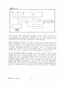


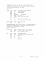
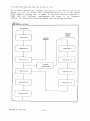

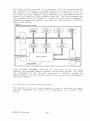
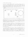
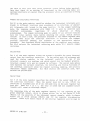
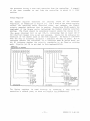
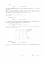
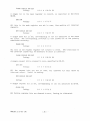
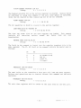


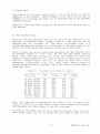
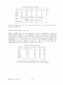
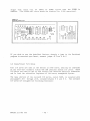
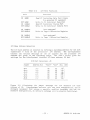
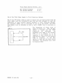


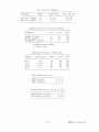


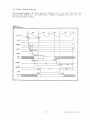
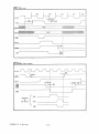


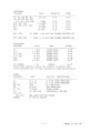
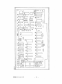

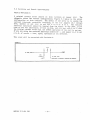


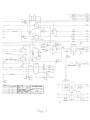
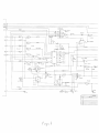
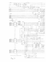
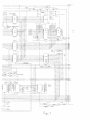


![mm [mm [1 um um [11115151116 |])|]1]](http://vs1.manualzilla.com/store/data/005839409_1-1dd2adaaab9a040f039445848c9c3135-150x150.png)