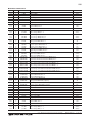
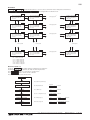
1
53U
OPERATING MANUAL
MULTI POWER MONITOR
(4 digital displays)
MODEL
53U
CONTENTS
BEFORE USE ................................................................................................................ 2
POINTS OF CAUTION....................................................................................................... 2
PERFORMANCE............................................................................................................. 3
LIGHTNING SURGE PROTECTION........................................................................................ 3
COMPONENT IDENTIFICATION........................................................................................... 4
INSTALLATION.............................................................................................................. 5
TERMINAL CONNECTIONS................................................................................................ 6
MODBUS WIRING CONNECTION......................................................................................... 8
SYSTEM CONFIGURATION EXAMPLES.................................................................................. 9
MODBUS - BASICS....................................................................................................... 10
MODBUS - OPERATIONS................................................................................................ 11
MODBUS - SETTING...................................................................................................... 13
MODBUS - MEASURED VARIABLES................................................................................... 26
OPERATION FLOWCHART............................................................................................... 38
SETTING EXAMPLES..................................................................................................... 48
ERROR MESSAGES....................................................................................................... 50
MAINTENANCE............................................................................................................ 50
5-2-55, Minamitsumori, Nishinari-ku, Osaka 557-0063 JAPAN
EM-6485-B
Phone: +81(6)6659-8201 Fax: +81(6)6659-8510 E-mail: [email protected]
Rev.18
P. 1 / 50
53U
BEFORE USE ....
Thank you for choosing M-System. Before use, please check
contents of the package you received as outlined below.
If you have any problems or questions with the product,
please contact M-System’s Sales Office or representatives.
■ PACKAGE INCLUDES:
Multi power monitor..................................................... (1)
■ MODEL NO.
Confirm Model No. marking on the product to be exactly
what you ordered.
■ OPERATING MANUAL
This manual describes necessary points of caution when
you use this product, including installation, connection, basic maintenance procedures, and detailed operations.
The 53U is programmable either by using the front control buttons or the PC Configurator Software. For detailed
information on the PC configuration, refer to the PMCFG
users manual. The PMCFG PC Configurator Software is
downloadable at M-System’s web site.
http://www.m-system.co.jp
Availability of certain functions explained in this manual
depends upon hardware options and firmware versions.
Those limited ones are identified with the following markings.
PMCFG users manual.
Software and manuals are downloadable at M-System’s
web site.
MARKING
AO
DO
DI
MO
1.01
2.00
2.40
LIMITATION
Analog output option
Discrete output option
Discrete input option
Modbus interface option
Ver.1.01 or higher versions
Ver.2.00 or higher versions
Ver.2.40 or higher versions
http://www.m-system.co.jp
• The equipment must be mounted inside a panel.
• For safety, be sure to install a circuit breaker switch as
part of the building installation that conforms to IEC
60947-1 and IEC 60947-3 near the 53U so as to be operated easily, and clearly indicate that the device is used to
de-energize the 53U. The circuit breaker must be provided
on both side of the line or must be “common trip” type.
• Insert a noise filter for the power source connected to the
unit. Cosel Noise Filter Model NAC-06-472 or equivalent
is recommended.
■ POWER INPUT RATING & OPERATIONAL RANGE
Locate the power input rating marked on the product and
confirm its operational range as indicated below.
100 – 240V AC rating: 85 – 264V AC, 47 – 66 Hz, <8VA
110 – 240V DC rating: 99 – 264V DC, <4W (UL approval
is not available)
• For UL approved model, power input terminals are marked
with L and N instead of U(+) and V(–).
■ GENERAL PRECAUTION
Before you remove or mount the unit, turn off the power
supply and input signal for safety.
■ ENVIRONMENT
•Indoor use
•Do not install the unit where it is directly exposed to rain,
water droplets or sunlight.
•When heavy dust or metal particles are present in the air,
install the unit inside proper housing with sufficient ventilation.
•Do not install the unit where it is subjected to continuous
vibration. Do not apply physical impact to the unit.
•Environmental temperature must be within -10 to +55°C
(14 to 131°F) with relative humidity within 90% RH in
order to ensure adequate life span and operation.
•Contrast of the LCD screen depends upon viewing angles. Choose the height and angle where it is the most legible.
•Do not apply physical impact to the front face.
•To ensure the designated ingress protection, insert the
gasket as shown below before attaching the mounting
brackets.
Mounting Bracket
■ INTENDED USE
This equipment is a digital panel meter which measures
simultaneously several variables of a heavy-current power
system: current, voltage, active, reactive and apparent power, active and reactive energy, power factor, frequency, etc.
■ SYMBOLS USED ON THE PRODUCT AND IN THIS MANUAL
This symbol on the product indicates that the operator
must refer to an explanation in the user’s manual in order
to avoid the risk of injury or death of personnel or damage
to the instrument.
This symbol indicates double insulation.
POINTS OF CAUTION
n CAUTION
If Equipment is not used in a manner not specified by MSystem, the protection provided by the equipment may be
impaired.
■ CONFORMITY WITH EC DIRECTIVES OR UL
•This equipment is suitable for use in a Pollution Degree 2
environment and in Measurement Category III, Installation Category II, with the maximum operating voltage of
550V between signal input and output or power and 300V
between output and power.
Prior to installation, check that the insulation class of this
unit satisfies the system requirements.
•Altitude up to 2000 meters
Panel
Gasket
■ WIRING
•Wiring to the unit must be conducted by qualified service
personnel.
•Do not install cables (power supply, input and output)
close to noise sources (relay drive cable, high frequency
line, etc.).
•Do not bind these cables together with those in which
noises are present. Do not install them in the same duct.
■ AND ....
The unit is designed to function as soon as power is supplied, however, a warm up for 30 minutes is required for satisfying complete performance described in the data sheet.
5-2-55, Minamitsumori, Nishinari-ku, Osaka 557-0063 JAPAN
EM-6485-B
Phone: +81(6)6659-8201 Fax: +81(6)6659-8510 E-mail: [email protected]
Rev.18
P. 2 / 50
53U
PERFORMANCE
LIGHTNING SURGE PROTECTION
Accuracy (at 23°C ±10°C or 73.4°F ±18°F, 45 – 65 Hz)
Voltage: ±0.3% (±0.2% for Option /H)*
Current: ±0.3% (±0.2% for Option /H)*
Power: ±0.5%*
Power factor: ±0.5%
Frequency: ±0.1%*
Energy: ±1% (±0.5% for Option /H)
Harmonic contents: ±1%*
Analog output: Accuracy of assigned measurand or
±0.2%, whichever is greater.
Response time: ≤2 seconds (0 – 99%)
≤3 seconds for frequency and harmonic contents
*In percentage of the spans: 480V for voltage, 1A or 5A for
current, 4155W (5A) or 831W (1A) for active power. The described accuracy levels are ensured at the input 1% or more
for phase 2 current with 3-phase/3-wire unbalanced load,
for neutral current with 3-phase/4-wire unbalanced load,
and neutral current with 1-phase/3-wire.
In order to protect the unit from lightning surges entering
through signal and power supply cables, use of appropriate
lightning surge protectors are recommended. Please contact M-System.
n INPUT
Frequency: 50 – 60 Hz
Voltage Input
Rated voltage:
Line-to-line (delta voltage): 480V
Line-neutral (phase voltage): 277V
(for single phase/2-wire and single phase/3-wire)
Consumption VA: ≤ ULN2 / 300kΩ / phase
Current Input
Rated current: 1A or 5A
Consumption VA: ≤ I2 · 0.01Ω / phase
Contact Input: 24V DC or 110V DC (input resistance 6kΩ)
Power input:
100 – 240V AC, 8VA max., 50 – 60 Hz
110 – 240V DC, 4W max. (UL approval is not available)
n OUTPUT
Network Interface
Interface: Conforms to EIA RS-485
Protocol: Modbus RTU
DC Current Output: 4 – 20mA DC, load resistance: 270Ω
maximum
DC Voltage Output: 1 – 5V DC, load resistance: 5000Ω
minimum
Open Collector
Programmable for either alarm or energy count.
Max. rated load: 130V DC @50mA
Continuous rated load: 130V DC @30mA
n Measurement category: CAT.III
n Power input installation category: CAT.II
The definition of the measurement category
CAT.I:
Circuits not directly connected to the main
power supply
CAT.II:
Circuits directly connected to low-voltage
facility
CAT.III:
Circuits in building facility
CAT.IV:
Power sources for low-voltage facility
5-2-55, Minamitsumori, Nishinari-ku, Osaka 557-0063 JAPAN
EM-6485-B
Phone: +81(6)6659-8201 Fax: +81(6)6659-8510 E-mail: [email protected]
Rev.18
P. 3 / 50
53U
COMPONENT IDENTIFICATION
■ FRONT VIEW
■ REAR VIEW
Voltage Input
Terminals
Data Displays
Current Input
Terminals
Power Input
Terminals
Control Buttons
∑
IU
PQS
PF THD
MAX
Configurator
Jack
Ext. Interface
Terminals
E PRG
ENTER ESCAPE
■ CONTROL BUTTON OPERATIONS
FUNCTIONS
BUTTON OPERATION
∑
IU
PQS
PF THD
MAX
ENTER
E PRG ESCAPE
∑
Hold down
IU
Hold down
E PRG ESCAPE Hold down
+
+
IU
∑
PQS
PF THD
Hold down
E PRG ESCAPE Hold down
Hold down
NORMAL MODE
Indicates values
Indicates Voltage or Current
Indicates Power
Indicates Power Factor or THD
SETTING MODE
Go Left
Go Right
Go Down
Go Up
Indicates totalized values
(max., min., average/demand)
Selects menu; Enables setting changes
Switches Energy readings
Switches to My Default mode
Switches to PC Configuration mode
Switches to Setting mode
Indicates Harmonics by degrees
Switches Energy reading units
Indicates the shortcut menu
Cancels setting changes
-------------------
■ HOW TO CHANGE VALUES (e.g. 5.000A to 150.0A)
press ∑
3 times
button
press PQS
5 times
press ∑
once
button
button
press PF THD
5 times
press ∑
once
button
button
press PF THD
once
button
Press
PQS
PF THD
Press
∑
IU
to increase or decrease the value.
to move between digits.
∑
Pressing
at the leftmost digit shifts the value on display to the right by 1 digit.
The decimal point and unit are also switched to appropriate ones.
5-2-55, Minamitsumori, Nishinari-ku, Osaka 557-0063 JAPAN
EM-6485-B
Phone: +81(6)6659-8201 Fax: +81(6)6659-8510 E-mail: [email protected]
Rev.18
P. 4 / 50
53U
INSTALLATION
■ EXTERNAL DIMENSIONS unit: mm (inch)
3 (.12)
80 (3.15)
[12 (.47)]
92 (3.62)
10
0(
96 (3.78)
3.9
4)
dia
.
92 (3.62)
23 (.91)
96 (3.78)
3 (.12)
2 (.08)
GASKET
MOUNTING BRACKET
■ PANEL CUTOUT unit: mm (inch)
+0.8 (3.65)
0 (3.63)
92
+0.8 (3.65)
0 (3.63)
92
Panel thickness : 2 to 15 mm (0.08 to 0.59 inch)
■ WIRING
• Current input
Applicable cable size: ≤ 2.4 mm dia., 0.5 to 3.5 mm2
Recommended core exposure length: 13 to 15 mm
• Voltage input
Applicable cable size: ≤ 2.5 mm dia., 0.5 to 3.5 mm2
Recommended core exposure length: 7 to 8 mm
• Output, power input
Applicable cable size: ≤ 2.4 mm dia., 0.5 to 2.5 mm2
Recommended core exposure length: 7 to 8 mm
n CONNECTING TO POWER SOURCE
• Confirm the power input rating on the specification label.
Rated voltage
AC Power
DC
Power*1
100 – 240 V AC
110 – 240 V DC
• How to Connect the power supply cable:
1) Confirm that the power supply is turned off.
2) Pull and remove the terminal block marked U(+) and
V(–)*2 from the 53U.
3) Loosen two (2) screws corresponding to U(+) and V(–)*2
at the terminal block.
4) Insert wires into the connection.
5) Fix them with the screw.
6) Replace the terminal block back into the 53U.
*1. UL approval is not available
*2. For UL approved model, L and N are marked.
5-2-55, Minamitsumori, Nishinari-ku, Osaka 557-0063 JAPAN
EM-6485-B
Phone: +81(6)6659-8201 Fax: +81(6)6659-8510 E-mail: [email protected]
Rev.18
P. 5 / 50
53U
TERMINAL CONNECTIONS
For UL approved model, L and N are marked instead of U(+) and V (–).
Input
V1 V2 V3 N 1S 1L 2S 2L 3S 3L
System /
Application
Terminal
V1 V2 V3 1S 1L 3S 3L
U
(+)
+ – + – T1 T2T3 T4
V
(–)
CONFIG
Power Input
V1 N
1S 1L
V1 N
source
L1
N
load
V1 N
u
source
L1
N
v
u
V
U
k
l
K
L
load
k
l
K
L
Three phase /
4-wire,
balanced load
load
load
v
v
u
V
V
U
k
l
K
L
l
k
l
K
L k
l
K
L
load
K
L
load
1S 1L
V1 N
load
V1 N
source
L1
L2
L3
N
source
L1
L2
L3
k
l
K
L
source
L1
L2
L3
N
1S 1L
k
l
K
L
load
1S 1L
v
U
V1
load
V
k
l
K
L
load
V2
V3
N 1S 1L 2S 2L 3S 3L
source
L1
L2
L3
N
V1 V2 V3 1S 1L
u
source
L1
L2
L3
V1 V2 V3 1S 1L
source
L1
L2
L3
U
l
L k
source
L1
L2
L3
N
u
V
k
K
V1 N
1S 1L
load
load
V1
V1 N V2 1S 1L 2S 2L
Single phase /
3-wire
v
V
v
U
source
L1
L2
L3
u
U
1S 1L
source
L1
N
V1 V2 V3 1S 1L
Three phase /
3-wire,
balanced load
source
L1
L2
L3
Terminal
load
V1 V2 V3 1S 1L 3S 3L
External Interface
System /
Application
Single phase /
2-wire
Three phase /
3-wire,
unbalanced load
Configurator Jack
DO/PO DI
source
L1
L2
L3
V1 V2 V3 1S 1L 3S 3L
source
L1
N
L2
Three phase /
4-wire,
unbalanced load
V1 N V2 1S 1L 2S 2L
load
source
L1
N
L2
k
l
K
L k
l
K
L
V2
V3
N 1S 1L 2S 2L 3S 3L
source
L1
L2
L3
N
k
l
K
L
k
l
K
L
load
k
l
K
L
load
V1
V2
V3
u v
u v
u v
U V
U V
U V
N
1S 1L 2S 2L 3S 3L
V1 N V2 1S 1L 2S 2L
source
L1
N
L2
u
v
v
u
U
V
V
U
k
l
K
L k
l
K
L
load
source
L1
L2
L3
N
k
l
K
L
k
K
load
l
k
l
K
L
L
5-2-55, Minamitsumori, Nishinari-ku, Osaka 557-0063 JAPAN
EM-6485-B
Phone: +81(6)6659-8201 Fax: +81(6)6659-8510 E-mail: [email protected]
Rev.18
P. 6 / 50
53U
■ EXTERNAL INTERFACE CODE: 2, 3
■ EXTERNAL INTERFACE CODE: 1
DI +
DI –
DO/PO+
T2
AO2 –
Jumper *1
T4
U(+)
AO2 +
Shielded Twisted-pair Cable
To other
Modbus devices
+
–
T3
Term.
Resist.
AO1 –
CONTACT
OUTPUT
DO/PO–
T1
AO1 +
CONTACT
INPUT
AO3 –
AO4 +
*3
AO4 –
POWER
V(–)
JACK
AO3 +
■ EXTERNAL INTERFACE CODE: 4, 5
AO1 +
AO1 –
AO2 +
AO2 –
DO/PO1+
ANALOG
OUTPUT 1
AO1 –
AO2 +
DO/PO1–
DO/PO2+
ANALOG
OUTPUT 2
AO2 –
U(+)
AO1 +
CONTACT
OUTPUT
DO/PO–
DO/PO2–
*3
JACK
V(–)
CONFIGURATOR *2
DO/PO1+
T1
T2
CONTACT OUTPUT 2
CONTACT OUTPUT 3
+
–
T3
Term.
Resist.
V(–)
JACK
DO/PO1–
DO/PO2+
DO/PO2–
Shielded Twisted-pair Cable
To other
Modbus devices
Jumper *1
T4
U(+)
JACK
DO/PO1+
CONTACT OUTPUT 1
DO/PO2+
DO/PO COM
DO/PO3+
DO/PO3–
DO/PO4+
*3
DO/PO4–
POWER
ANALOG
OUTPUT 1
ANALOG
OUTPUT 2
CONTACT
OUTPUT 1
CONTACT
OUTPUT 2
POWER
CONFIGURATOR *2
CONTACT
OUTPUT 1
CONTACT
OUTPUT 2
CONTACT
OUTPUT 3
CONTACT
OUTPUT 4
U(+) *3
CONFIGURATOR
V(–)
JACK
• Contact Input Connection E.g.
CONFIGURATOR *2
■ EXTERNAL INTERFACE CODE: 9
■ EXTERNAL INTERFACE CODE: 8
DO/PO3+
POWER
3
U(+) *
POWER
V(–)
ANALOG
OUTPUT 4
■ EXTERNAL INTERFACE CODE: 6, 7
CONTACT
INPUT
DO/PO+
ANALOG
OUTPUT 3
V(–)
JACK
DI –
ANALOG
OUTPUT 2
3
U(+) *
CONFIGURATOR
DI +
ANALOG
OUTPUT 1
POWER
CONFIGURATOR
• Contact Output Connection E.g.
DI +
+
DO/PO+
+
DI –
-
DO/PO–
-
*1. When the device is located at the end of a transmission line via
twisted-pair cable, (when there is no cross-wiring), close across the
terminal T2 – T3 with a leadwire.
When the device is not at the end, no shortcircuit wire is required.
*2. Analog output may momentarily fluctuate while the configurator cable
is left connected.
*3. For UL approved model, L and N are marked, instead of U(+) and V(–).
5-2-55, Minamitsumori, Nishinari-ku, Osaka 557-0063 JAPAN
EM-6485-B
Phone: +81(6)6659-8201 Fax: +81(6)6659-8510 E-mail: [email protected]
Rev.18
P. 7 / 50
53U
MODBUS WIRING CONNECTION
RS-232-C
CONNECTOR
R2K-1
RS-485
T1
T2
T3
T4
53U
RS-485
53U
T1
T2
T3
T4
*1
T1
T2
T3
T4
*1
FG *
*1. Internal terminating resistor is used when the device is at the end of a transmission line.
*2. Install shield cables to all sections and ground them at single point.
2
5-2-55, Minamitsumori, Nishinari-ku, Osaka 557-0063 JAPAN
EM-6485-B
Phone: +81(6)6659-8201 Fax: +81(6)6659-8510 E-mail: [email protected]
Rev.18
P. 8 / 50
53U
SYSTEM CONFIGURATION EXAMPLES
■ RS-485 / RS-232-C
RS-232-C
RS-232-C/RS-485
Converter
(model: R2K-1 or LK1)
Lightning Surge Protector
for RS-485/422
(model: MD74R or MDP-4R) *1
RS-485 (Modbus RTU)
Lightning Surge Protector
for RS-485/422
(model: MD74R or MDP-4R) *1
AX
IN
AX
IN
AX
IN
Multi Power Monitor
(model: 53U)
■ RS-485 / ETHERNET
Ethernet
Communication Adaptor
(model: 72EM-M4 or 72EM2-M4)
ETHERNET
RUN
SEND
FIELD
CNFG
Lightning Surge Protector
for RS-485/422
(model: MD74R or MDP-4R) *1
RS-485 (Modbus RTU)
Lightning Surge Protector
for RS-485/422
(model: MD74R or MDP-4R) *1
AX
IN
AX
IN
AX
IN
Multi Power Monitor
(model: 53U)
*1. Insert lightning surge protectors recommended in this example if necessary.
5-2-55, Minamitsumori, Nishinari-ku, Osaka 557-0063 JAPAN
EM-6485-B
Phone: +81(6)6659-8201 Fax: +81(6)6659-8510 E-mail: [email protected]
Rev.18
P. 9 / 50
53U
MODBUS - BASICS
This device conforms with Modbus-RTU protocol (MODBUS APPLICATION PROTOCOL V1.1a / Modbus over Serial Line
Specification & Implementation Guide V1.0).
The following communication parameters are selectable.
COMM. PROPERTY
SELECTION
Modbus address
1 to 247
Baud rate
1200 bps
2400 bps
4800 bps
9600 bps
19200 bps
38400 bps (*)
Parity bit
None
Odd (*)
Even
Stop bit
1 bit (*)
2 bits
T1.5 timer length
0 to 6.0, in 0.1 increments (Modbus protocol standard: 1.5)
T3.5 timer length
0 to 6.0, in 0.1 increments (Modbus protocol standard: 3.5)
(*) Factory setting
When appropriately set, the host PC connected via RS-485 can read measurands from and write configurations (setting) to
the device.
All registers are assigned to Read Holding Registers, can be read out using this command. If reading an address with no assigned register is attempted, ‘0’ is given.
Write Multiple Registers command is used to write registers. If writing an address with no assigned register is attempted,
‘Exception’ is given.
FUNCTION CODE
03
16
COMMAND
Read Holding Registers
Write Multiple Registers
RECOMMENDED TIME OUT VALUE
0.5 second
2 seconds
These commands enable reading measurands and writing configurations.
One (1) word registers are represented in 16-bit integers, while two (2) word registers are in 32-bit. All registers are in the
form of integer unless specifically given in the explanations.
The lower digit word in a 32-bit register is assigned to the lower address (n), while the upper digit word is assigned to the
higher address (n+1). The order can be reversed by programming.
The 32-bit register must be read out and written in single command sequence.
CAUTION : DO NOT apply new setting via Modbus and the front control buttons at once.
It is recommended to wait for a time period indicated under ‘recommended time out value’ in the above table to receive a response for a command. If no response is received for these time periods, take appropriate error processing such as retrying.
5-2-55, Minamitsumori, Nishinari-ku, Osaka 557-0063 JAPAN
EM-6485-B
Phone: +81(6)6659-8201 Fax: +81(6)6659-8510 E-mail: [email protected]
Rev.18
P. 10 / 50
53U
MODBUS - OPERATIONS
Modbus registers are assigned to program and operate the unit via Modbus network. It can also disable the view switching
control via the front keys to fix the display view to a specific parameter combination.
■ MODBUS REGISTER ACCESS SETTING
ADDR. WORDPARAMETER
4943
2
Deactivate Modbus register writing protection 1.01
Writing a preset passcode in this register deactivates the writing protection via Modbus.
When the Modbus passcode set in this register matches the preset one, setting ‘1’ or ‘2’ in the register address 4945 becomes available to enable writing in Modbus registers.
Reading out the register value is not possible. It reads always ‘-1’ regardless of the code setting.
After writing is complete, be sure to set a value other than the passcode (‘0’ is recommended) to activate the writing protection again.
4945
1
Modbus register access setting
0 : Write disable (*)
1 : Write enable
2 : Write enable the count values
Other : Write disable
This setting is erased when the power supply to the unit is removed. It always starts with ‘0’ (Write disable) when the power supply is turned on. Set ‘1’ or ‘2’ before starting writing at other registers.
In order to write a count value (e.g. active energy), set ‘2’ at this register address. When it is set, the unit stops counting so that a new count value can be written in the register address. Be careful to use ‘2’ setting because no counting will be performed if the unit remains with this setting.
When the Modbus register writing protection is enabled, this register setting cannot be changed from ‘0’ to ‘1’ or ‘2’ unless a correct security code is set in the register address 4943.
■ USER OPERATIONS
User operations include switching the display views and resetting alarm trips.
ADDR. WORDPARAMETER
5201
1
Key operation lock
0 : All key operations available (*)
1 : All key operations locked
2 : Lock the key operation to go to Setting mode only
5202
1
Data reading display
Shows the parameter set displayed on the three data displays. The display can be switched by writing at this address from the host.
5203
1
Energy reading display
Shows the parameter type displayed on the bottom data display. The display can be switched by writing at this address from the host.
5204
1
Energy reading display unit
0 : 0.1 kWh, 0.1 kvarh, 0.1 kVA (*)
1 : 0.1 Wh, 0.1 varh, 0.1 VA
Shows the unit (factor) of the parameter on the energy display (k = kilo). The display unit can be switched by writing at this address from the host.
Exception: Count time (unit: h) is displayed always ‘without kilo’.
5205
1
Reset alarm trip
1 : Reset
0 : No resetting
5206
1
Automatic ∑ view switching
0 : Disable automatic switching (*)
1 : Enable automatic switching: ∑1 through ∑4 switched in 10 second intervals. Automatic switching is cancelled when one of the front control buttons are touched.
5-2-55, Minamitsumori, Nishinari-ku, Osaka 557-0063 JAPAN
EM-6485-B
Phone: +81(6)6659-8201 Fax: +81(6)6659-8510 E-mail: [email protected]
Rev.18
P. 11 / 50
53U
■ SYSTEM OPERATIONS
System operations include switching the tariff or resetting energy counts, and rebooting.
ADDR. WORDPARAMETER
5329
1
Switch tariff
0 : High tariff (peak time) (*)
1 : Low tariff (off-peak time)
5330
1
Reset energy count
1 : Reset all values
2 : Reset all MAX / MIN values and set the present values.
3 : Reset all average (demand) values
0 : No resetting
Specify the extent of count resetting. The register is automatically set to ‘0’ when the resetting procedure is complete after one of these values is written at this address. If another value is written before ‘0’ has been set, the former resetting procedure ends indefinitely.
Specific values can be preset to each register by writing at this address from the host.
5331
1
Reboot system
Write ‘10001’ to reboot the system. (Any other values can be written but invalid.)
5332
1
Backup / restore setting
20002 : Backup the present setting
30003 : Restore the device with the backup setting data
The register is automatically set to ‘0’ when the procedure is complete after one of these values is written at this address. If another value is written before ‘0’ has been set, the former procedure ends indefinitely.
5333
1
Passcode
0000 to 9999
0000 : Factory setting
Set and read out a passcode used to go into the Setting Mode using the front control keys.
5334
2
Modbus register writing protection passcode 1.01
Setting a passcode to control writing registers via Modbus.
1 to 999 999 999
0 : Cancel writing protection (*)
The Modbus passcode must be set to the register address 4943 before setting ‘1’ or ‘2’ in the address 4945 to deactivate the writing protection.
The value in this register is encripted when it is read out. Only ‘0’ (Cancel protection) is read out as it is.
When a new code is set in this register, the register address 4945 is immediately reset to ‘0’ so that a next com-
mand will be already limited in access.
5-2-55, Minamitsumori, Nishinari-ku, Osaka 557-0063 JAPAN
EM-6485-B
Phone: +81(6)6659-8201 Fax: +81(6)6659-8510 E-mail: [email protected]
Rev.18
P. 12 / 50
53U
MODBUS - SETTING
■ SYSTEM SETTING
ADDR. WORDPARAMETER
UNIT
5601
1
System configuration
0 : Single-phase / 2-wire (1CT)
1 : Single-phase / 3-wire (2CT)
2 : 3-phase / 3-wire, balanced load (1CT)
3 : 3-phase / 3-wire, unbalanced load (2CT)
4 : 3-phase / 4-wire, balanced load (1CT)
5 : 3-phase / 4-wire, unbalanced load (3CT) (*)
5602
1
CT rating, Primary
A
1 to 20 000 : Current (A)
Factory setting : 1 or 5
5603
1
CT rating, Secondary
A
1 : 1A
5 : 5A
Factory setting : 1 or 5
5604
1
VT rating, Primary
V
50 to 400 000 : Voltage (V)
Factory setting : 110
5606
1
VT rating, Secondary
V
50 to 500 : Voltage (V)
Factory setting : 110
5607
1
Frequency input
--- 0 : Voltage (*)
1 : Current
2 : Fixed to 50Hz 2.40
3 : Fixed to 60Hz 2.40
Fixed to 50Hz/60Hz should not be used in normal circumstances.
5608
1
Low-end cutout, Current
%/10
0 to 999 : Rated current × 0.001 × Specified value
Factory setting : 10
5609
1
Low-end cutout, Voltage
%/10
0 to 999 : Rated voltage × 0.001 × Specified value
Factory setting : 10
■ MODBUS SETTING
The device must be reset or the power supply to it must be turned off and on in order to enable the Modbus setting.
ADDR. WORDPARAMETER
5729
1
Modbus address
1 to 247
Factory setting : 1
5730
1
Baud rate
0 : 1200
1 : 2400
2 : 4800
3 : 9600
4 : 19200 5 : 38400 (*)
5731
1
Parity bit
0 : None
1 : Odd (*)
2 : Even
5732
1
Stop bit
0 : 1 bit (*)
1 : 2 bits
5733
1
T1.5 timer length
1 to 60 : Specified value × 0.1 character length
Factory setting : 15
5734
1
T3.5 timer length
1 to 60 : Specified value × 0.1 character length
Factory setting : 35
5735
1
Long register (32-bit words assignments)
0 : Normal (*)
Lower digit word at the lower address
1 : Swap
Lower digit word at the higher address
5-2-55, Minamitsumori, Nishinari-ku, Osaka 557-0063 JAPAN
EM-6485-B
Phone: +81(6)6659-8201 Fax: +81(6)6659-8510 E-mail: [email protected]
Rev.18
P. 13 / 50
53U
■ DEMAND SETTING
ADDR. WORDPARAMETER
5857
1
Average (demand) current update interval
0 : External trigger signal
1 to 60 : Minutes
Factory setting : 30
5858
1
Average (demand) power update interval
0 : External trigger signal
1 to 60 : Minutes
Factory setting : 30
UNIT
Minutes
Minutes
■ STYLE SETTING
ADDR. WORDPARAMETER
5985
1
Input line indication
0 : 1 – 2 – 3 (*)
1:R–S–T
5986
1
Phase difference direction indication
0 : IND / CAP (*)
1 : LEAD / LAG
5987
1
Power factor (PF1 through PF3, PF) sign
0 : Standard (IEC) (*)
Identical to the active energy
1 : Special type 1 (IEEE) Positive in LAG, Negative in LEAD
5988
1
Reactive power (Q1 through Q3, Q) sign
0 : Standard (IEC) (*)
Positive from [PF = 1.0] to 180° in LAG direction; Negative for the other direction
1 : Special type 1
Positive in LAG, Negative in LEAD
5989
1
Reactive power (Q1 through Q3) calculation (Q = Q1 + Q2 + Q3)
__________
2
2
0 : Standard (*)
Qn = √ Sn – Pn Nsmp
1
1 : Reactive power meter method Qn = –––––– ∑ (Un
i – Nui) I i + (Nsmp / 4)
Nsmp i = 1
5990
1
Apparent power (S) calculation
________
0 : Standard (*) S = √ P2 + Q2
1 : Sum
S = S1 + S2 + S3
5991
1
Unit used to indicate power up to 9999 2.00
0 : With ‘k’ (0.000 k) (*)
1 : Without ‘k’ (0000)
Note: ‘1,’ ‘2,’ ‘3’ in expressions like Q1, Q2, Q3 indicate ‘R,’ ‘S,’ ‘T’ respectively.
■ DISCRETE I/O SETTING DO DI
ADDR. WORDPARAMETER
6113
1
Discrete output 1 function
0 : Undefined (*)
1 : Energy count
2 : Alarm
6114
1
Discrete output 1 contact type
0 : Normally open contact (*)
1 : Normally closed contact
The contact opens at the power OFF regardless of this setting.
6115
1
Discrete input function
0 : Undefined (*)
1 : Update demand
2 : Reset energy count
3 : Reset alarm trip
4 : Tariff setting for Energy count (ON: high tariff)
6116
1
Discrete input contact type
0 : Normally open contact (*)
1 : Normally closed contact
6117
1
Discrete output 2 function
0 : Undefined (*)
1 : Energy count
2 : Alarm
6118
1
Discrete output 2 contact type
0 : Normally open contact (*)
1 : Normally closed contact
The contact opens at the power OFF regardless of this setting.
5-2-55, Minamitsumori, Nishinari-ku, Osaka 557-0063 JAPAN
EM-6485-B
Phone: +81(6)6659-8201 Fax: +81(6)6659-8510 E-mail: [email protected]
Rev.18
P. 14 / 50
53U
ADDR. WORDPARAMETER
6121
1
6122
1
6125
1
6126
1
Discrete output 3 function
0 : Undefined (*)
1 : Energy count
2 : Alarm
Discrete output 3 contact type
0 : Normally open contact (*)
1 : Normally closed contact
The contact opens at the power OFF regardless of this setting.
Discrete output 4 function
0 : Undefined (*)
1 : Energy count
2 : Alarm
Discrete output 4 contact type
0 : Normally open contact (*)
1 : Normally closed contact
The contact opens at the power OFF regardless of this setting.
■ ENERGY SETTING DO
ADDR. WORDPARAMETER
6241
1
Energy count 1 assigned to the discrete output 1
Refer to the table in the following page.
6242
2
Pulse weight for Energy count 1
0 : No pulse output (disabled)
1 to 100 000 : Specified value × 0.1 (kWh / kvarh / kVA)
Factory setting : 10
6244
1
Pulse duration (width) for Energy count 1
1 to 20 : Specified value × 100 msec.
Factory setting : 1
6245
1
Tariff setting for Energy count 1
0 : Disable (*)
1 : Enable
6246
1
Energy count 2 assigned to the discrete output 2
Refer to the table in the following page.
6247
2
Pulse weight for Energy count 2
0 : No pulse output (disabled)
1 to 100 000 : Specified value × 0.1 (kWh / kvarh / kVA)
Factory setting : 10
6249
1
Pulse duration (width) for Energy count 2
1 to 20 : Specified value × 100 msec.
Factory setting : 1
6250
1
Energy count 3 assigned to the discrete output 3
Refer to the table in the following page.
6251
2
Pulse weight for Energy count 3
0 : No pulse output (disabled)
1 to 100 000 : Specified value × 0.1 (kWh / kvarh / kVA)
Factory setting : 10
6253
1
Pulse duration (width) for Energy count 3
1 to 20 : Specified value × 100 msec.
Factory setting : 1
6254
1
Energy count 4 assigned to the discrete output 4
Refer to the table in the following page.
6255
2
Pulse weight for Energy count 4
0 : No pulse output (disabled)
1 to 100 000 : Specified value × 0.1 (kWh / kvarh / kVA)
Factory setting : 10
6257
1
Pulse duration (width) for Energy count 4
1 to 20 : Specified value × 100 msec.
Factory setting : 1
5-2-55, Minamitsumori, Nishinari-ku, Osaka 557-0063 JAPAN
EM-6485-B
Phone: +81(6)6659-8201 Fax: +81(6)6659-8510 E-mail: [email protected]
UNIT
---kWh / 10
kvarh / 10
kVA / 10
sec / 10
----
---kWh / 10
kvarh / 10
kVA / 10
sec / 10
---kWh / 10
kvarh / 10
kVA / 10
sec / 10
---kWh / 10
kvarh / 10
kVA / 10
sec / 10
Rev.18
P. 15 / 50
53U
Energy count type
SET VALUE
0
1
2
3
4
5
6
7
8
9
10
11
12
13
200
201
202
203
204
205
206
207
208
209
210
211
212
213
300
301
302
303
304
305
306
307
308
309
310
311
312
313
ID
T-EP
T-EQ
T-ES
T-EP–
T-EQ–
T-EQ+LAG
T-EQ+LEAD
T-EQ–LAG
T-EQ–LEAD
----
T-EQ+P
T-EQ–P
T-EPA
T-EQA
EP
EQ
ES
EP–
EQ–
EQ+LAG
EQ+LEAD
EQ–LAG
EQ–LEAD
----
EQ+P
EQ–P
EPA
EQA
L-EP
L-EQ
L-ES
L-EP–
L-EQ–
L-EQ+LAG
L-EQ+LEAD
L-EQ–LAG
L-EQ–LEAD
----
L-EQ+P
L-EQ–P
L-EPA
L-EQA
PARAMETER
Active energy, incoming (*)
Reactive energy, LAG
Apparent energy
Active energy, outgoing
Reactive energy, LEAD
Reactive energy, incoming, LAG
Reactive energy, incoming, LEAD
Reactive energy, outgoing, LAG
Reactive energy, outgoing, LEAD
Reserved. DO NOT USE.
Reactive energy, incoming
Reactive energy, outgoing
Active energy, (incoming – outgoing)
Reactive energy, (incoming + outgoing)
Active energy, high tariff, incoming
Reactive energy, high tariff, LAG
Apparent energy, high tariff
Active energy, high tariff, outgoing
Reactive energy, high tariff, LEAD
Reactive energy, high tariff, incoming, LAG
Reactive energy, high tariff, incoming, LEAD
Reactive energy, high tariff, outgoing, LAG
Reactive energy, high tariff, outgoing, LEAD
Reserved. DO NOT USE.
Reactive energy, high tariff, incoming
Reactive energy, high tariff, outgoing
Active energy, high tariff, (incoming – outgoing)
Reactive energy, high tariff, (incoming + outgoing)
Active energy, low tariff, incoming
Reactive energy, low tariff, LAG
Apparent energy, low tariff
Active energy, low tariff, outgoing
Reactive energy, low tariff, LEAD
Reactive energy, low tariff, incoming, LAG
Reactive energy, low tariff, incoming, LEAD
Reactive energy, low tariff, outgoing, LAG
Reactive energy, low tariff, outgoing, LEAD
Reserved. DO NOT USE.
Reactive energy, low tariff, incoming
Reactive energy, low tariff, outgoing
Active energy, low tariff, (incoming – outgoing)
Reactive energy, low tariff, (incoming + outgoing)
5-2-55, Minamitsumori, Nishinari-ku, Osaka 557-0063 JAPAN
EM-6485-B
Phone: +81(6)6659-8201 Fax: +81(6)6659-8510 E-mail: [email protected]
2.00
2.00
2.00
2.00
2.00
2.00
2.00
2.00
2.00
2.00
2.00
2.00
2.00
2.00
2.00
2.00
2.00
2.00
2.00
2.00
2.00
2.00
2.00
2.00
2.00
2.00
2.00
2.00
2.00
2.00
2.00
2.00
Rev.18
P. 16 / 50
53U
■ ALARM SETTING
ADDR. WORDPARAMETER
6369
1
Power ON delay time
0 to 999 : Seconds
Factory setting : 0
6370
1
Latching
0 : No latching (*)
1 : Latching (Alarm trip is held until a reset command is received or power OFF)
6371
2
I1 thr. I3 - Current : High setpoint
Factory setting : 0
6373
2
I1 thr. I3 - Current : Low setpoint
Factory setting : 0
6375
1
I1 thr. I3 - Current : Alarm output
0 : Disable (*)
1 : Display only
2 : Display + contact output
6376
1
I1 thr. I3 - Current : Hysteresis (deadband)
0 to 999 : Specified value × 0.1 (%)
Factory setting : 0
6377
1
I1 thr. I3 - Current : ON delay time
0 to 999 : Seconds
Factory setting : 0
6379
2
IN - Neutral current : High setpoint
Factory setting : 0
6381
2
IN - Neutral current : Low setpoint
Factory setting : 0
6383
1
IN - Neutral current : Alarm output
0 : Disable (*)
1 : Display only
2 : Display + contact output
6384
1
IN - Neutral current : Hysteresis (deadband)
0 to 999 : Specified value × 0.1 (%)
Factory setting : 0
6385
1
IN - Neutral current : ON delay time
0 to 999 : Seconds
Factory setting : 0
6387
2
U12 thr. U31 - Delta voltage : High setpoint
Factory setting : 0
6389
2
U12 thr. U31 - Delta voltage : Low setpoint
Factory setting : 0
6391
1
U12 thr. U31 - Delta voltage : Alarm output
0 : Disable (*)
1 : Display only
2 : Display + contact output
6392
1
U12 thr. U31 - Delta voltage : Hysteresis (deadband)
0 to 999 : Specified value × 0.1 (%)
Factory setting : 0
6393
1
U12 thr. U31 - Delta voltage : ON delay time
0 to 999 : Seconds
Factory setting : 0
6395
2
U1N thr. U3N - Phase voltage : High setpoint
Factory setting : 0
6397
2
U1N thr. U3N - Phase voltage : Low setpoint
Factory setting : 0
6399
1
U1N thr. U3N - Phase voltage : Alarm output
0 : Disable (*)
1 : Display only
2 : Display + contact output
6400
1
U1N thr. U3N - Phase voltage : Hysteresis (deadband)
0 to 999 : Specified value × 0.1 (%)
Factory setting : 0
6401
1
U1N thr. U3N - Phase voltage : ON delay time
0 to 999 : Seconds
Factory setting : 0
5-2-55, Minamitsumori, Nishinari-ku, Osaka 557-0063 JAPAN
EM-6485-B
Phone: +81(6)6659-8201 Fax: +81(6)6659-8510 E-mail: [email protected]
UNIT
Seconds
----
mA
mA
----
%/10
Seconds
mA
mA
----
%/10
Seconds
V/100
V/100
----
%/10
Seconds
V/100
V/100
----
%/10
Seconds
Rev.18
P. 17 / 50
53U
ADDR. WORDPARAMETER
6403
2
6405
2
6407
1
6408
1
6409
1
6411
2
6413
2
6415
1
6416
1
6417
1
6419
2
6421
2
6423
1
6424
1
6425
1
6427
2
6429
2
6431
1
6432
1
6433
1
UNIT
P - Active power : High setpoint
Factory setting : 0
P - Active power : Low setpoint
Factory setting : 0
P - Active power : Alarm output
0 : Disable (*)
1 : Display only
2 : Display + contact output
P - Active power : Hysteresis (deadband)
0 to 999 : Specified value × 0.1 (%)
Factory setting : 0
P - Active power : ON delay time
0 to 999 : Seconds
Factory setting : 0
Q - Reactive power : High setpoint
Factory setting : 0
Q - Reactive power : Low setpoint
Factory setting : 0
Q - Reactive power : Alarm output
0 : Disable (*)
1 : Display only
2 : Display + contact output
Q - Reactive power : Hysteresis (deadband)
0 to 999 : Specified value × 0.1 (%)
Factory setting : 0
Q - Reactive power : ON delay time
0 to 999 : Seconds
Factory setting : 0
S - Apparent power : High setpoint
Factory setting : 0
S - Apparent power : Low setpoint
Factory setting : 0
S - Apparent power : Alarm output
0 : Disable (*)
1 : Display only
2 : Display + contact output
S - Apparent power : Hysteresis (deadband)
0 to 999 : Specified value × 0.1 (%)
Factory setting : 0
S - Apparent power : ON delay time
0 to 999 : Seconds
Factory setting : 0
PF - Power factor : High setpoint
Factory setting : 0
PF - Power factor : Low setpoint
Factory setting : 0
PF - Power factor : Alarm output
0 : Disable (*)
1 : Display only
2 : Display + contact output
PF - Power factor : Hysteresis (deadband)
0 to 999 : Specified value × 0.1 (%)
Factory setting : 0
PF - Power factor : ON delay time
0 to 999 : Seconds
Factory setting : 0
5-2-55, Minamitsumori, Nishinari-ku, Osaka 557-0063 JAPAN
EM-6485-B
Phone: +81(6)6659-8201 Fax: +81(6)6659-8510 E-mail: [email protected]
W
W
----
%/10
Seconds
var
var
----
%/10
Seconds
VA
VA
----
%/10
Seconds
%/100
%/100
----
%/10
Seconds
Rev.18
P. 18 / 50
53U
ADDR. WORDPARAMETER
6435
2
6437
2
6439
1
6440
1
6441
1
6443
2
6445
2
6447
1
6448
1
6449
1
6451
2
6453
2
6455
1
6456
1
6457
1
6459
2
6461
2
6463
1
6464
1
6465
1
UNIT
F - Frequency : High setpoint
Factory setting : 6500
F - Frequency : Low setpoint
Factory setting : 4500
F - Frequency : Alarm output
0 : Disable (*)
1 : Display only
2 : Display + contact output
F - Frequency : Hysteresis (deadband)
0 to 999 : Specified value × 0.1 (%)
Factory setting : 0
F - Frequency : ON delay time
0 to 999 : Seconds
Factory setting : 0
I1 AVG thr. I3 AVG - Average (demand) current : High setpoint
Factory setting : 0
I1 AVG thr. I3 AVG - Average (demand) current : Low setpoint
Factory setting : 0
I1 AVG thr. I3 AVG - Average (demand) current : Alarm output
0 : Disable (*)
1 : Display only
2 : Display + contact output
I1 AVG thr. I3 AVG - Average (demand) current : Hysteresis (deadband)
0 to 999 : Specified value × 0.1 (%)
Factory setting : 0
I1 AVG thr. I3 AVG - Average (demand) current : ON delay time
0 to 999 : Seconds
Factory setting : 0
IN AVG - Average (demand) neutral current : High setpoint
Factory setting : 0
IN AVG - Average (demand) neutral current : Low setpoint
Factory setting : 0
IN AVG - Average (demand) neutral current : Alarm output
0 : Disable (*)
1 : Display only
2 : Display + contact output
IN AVG - Average (demand) neutral current : Hysteresis (deadband)
0 to 999 : Specified value × 0.1 (%)
Factory setting : 0
IN AVG - Average (demand) neutral current : ON delay time
0 to 999 : Seconds
Factory setting : 0
P AVG - Average (demand) active power : High setpoint
Factory setting : 0
P AVG - Average (demand) active power : Low setpoint
Factory setting : 0
P AVG - Average (demand) active power : Alarm output
0 : Disable (*)
1 : Display only
2 : Display + contact output
P AVG - Average (demand) active power : Hysteresis (deadband)
0 to 999 : Specified value × 0.1 (%)
Factory setting : 0
P AVG - Average (demand) active power : ON delay time
0 to 999 : Seconds
Factory setting : 0
5-2-55, Minamitsumori, Nishinari-ku, Osaka 557-0063 JAPAN
EM-6485-B
Phone: +81(6)6659-8201 Fax: +81(6)6659-8510 E-mail: [email protected]
Hz/100
Hz/100
----
%/10
Seconds
mA
mA
----
%/10
Seconds
mA
mA
----
%/10
Seconds
W
W
----
%/10
Seconds
Rev.18
P. 19 / 50
53U
ADDR. WORDPARAMETER
6467
2
6469
2
6471
1
6472
1
6473
1
6475
2
6477
2
6479
1
6480
1
6481
1
6483
2
6485
2
6487
1
6488
1
6489
1
6491
2
6493
2
6495
1
6496
1
6497
1
UNIT
Q AVG - Average (demand) reactive power : High setpoint
Factory setting : 0
Q AVG - Average (demand) reactive power : Low setpoint
Factory setting : 0
Q AVG - Average (demand) reactive power : Alarm output
0 : Disable (*)
1 : Display only
2 : Display + contact output
Q AVG - Average (demand) reactive power : Hysteresis (deadband)
0 to 999 : Specified value × 0.1 (%)
Factory setting : 0
Q AVG - Average (demand) reactive power : ON delay time
0 to 999 : Seconds
Factory setting : 0
S AVG - Average (demand) apparent power : High setpoint
Factory setting : 0
S AVG - Average (demand) apparent power : Low setpoint
Factory setting : 0
S AVG - Average (demand) apparent power : Alarm output
0 : Disable (*)
1 : Display only
2 : Display + contact output
S AVG - Average (demand) apparent power : Hysteresis (deadband)
0 to 999 : Specified value × 0.1 (%)
Factory setting : 0
S AVG - Average (demand) apparent power : ON delay time
0 to 999 : Seconds
Factory setting : 0
THDI1 thr. THDI3 - Current total harmonic distortion : High setpoint
Factory setting : 0
THDI1 thr. THDI3 - Current total harmonic distortion : Low setpoint
Factory setting : 0
THDI1 thr. THDI3 - Current total harmonic distortion : Alarm output
0 : Disable (*)
1 : Display only
2 : Display + contact output
THDI1 thr. THDI3 - Current total harmonic distortion : Hysteresis (deadband)
0 to 999 : Specified value × 0.1 (%)
Factory setting : 0
THDI1 thr. THDI3 - Current total harmonic distortion : ON delay time
0 to 999 : Seconds
Factory setting : 0
THDIN - Neutral current total harmonic distortion : High setpoint
Factory setting : 0
THDIN - Neutral current total harmonic distortion : Low setpoint
Factory setting : 0
THDIN - Neutral current total harmonic distortion : Alarm output
0 : Disable (*)
1 : Display only
2 : Display + contact output
THDIN - Neutral current total harmonic distortion : Hysteresis (deadband)
0 to 999 : Specified value × 0.1 (%)
Factory setting : 0
THDIN - Neutral current total harmonic distortion : ON delay time
0 to 999 : Seconds
Factory setting : 0
5-2-55, Minamitsumori, Nishinari-ku, Osaka 557-0063 JAPAN
EM-6485-B
Phone: +81(6)6659-8201 Fax: +81(6)6659-8510 E-mail: [email protected]
var
var
----
%/10
Seconds
VA
VA
----
%/10
Seconds
%/10
%/10
----
%/10
Seconds
%/10
%/10
----
%/10
Seconds
Rev.18
P. 20 / 50
53U
ADDR. WORDPARAMETER
6499
2
6501
2
6503
1
6504
1
6505
1
6507
2
6509
2
6511
1
6512
1
6513
1
6515
2
6517
2
6519
1
6520
1
6521
1
UNIT
THDU12 thr. THDU31 - Delta voltage total harmonic distortion : High setpoint
%/10
Factory setting : 0
THDU12 thr. THDU31 - Delta voltage total harmonic distortion : Low setpoint
%/10
Factory setting : 0
THDU12 thr. THDU31 - Delta voltage total harmonic distortion : Alarm output
---0 : Disable (*)
1 : Display only
2 : Display + contact output
THDU12 thr. THDU31 - Delta voltage total harmonic distortion : Hysteresis (deadband)
%/10
0 to 999 : Specified value × 0.1 (%)
Factory setting : 0
THDU12 thr. THDU31 - Delta voltage total harmonic distortion : ON delay time
Seconds
0 to 999 : Seconds
Factory setting : 0
THDU1N thr. THDU3N - Phase voltage total harmonic distortion : High setpoint
%/10
Factory setting : 0
THDU1N thr. THDU3N - Phase voltage total harmonic distortion : Low setpoint
%/10
Factory setting : 0
THDU1N thr. THDU3N - Phase voltage total harmonic distortion : Alarm output
---0 : Disable (*)
1 : Display only
2 : Display + contact output
THDU1N thr. THDU3N - Phase voltage total harmonic distortion : Hysteresis (deadband)
%/10
0 to 999 : Specified value × 0.1 (%)
Factory setting : 0
THDU1N thr. THDU3N - Phase voltage total harmonic distortion : ON delay time
Seconds
0 to 999 : Seconds
Factory setting : 0
UT12 thr. UT31 - Phase angle between phase voltages : High setpoint 2.00
°
Factory setting : 0
UT12 thr. UT31 - Phase angle between phase voltages : Low setpoint 2.00
°
Factory setting : 0
UT12 thr. UT31 - Phase angle between phase voltages : Alarm output 2.00---0 : Disable (*)
1 : Display only
2 : Display + contact output
UT12 thr. UT31 - Phase angle between phase voltages : Hysteresis (deadband) 2.00
%/10
0 to 999 : Specified value × 0.1 (%)
Factory setting : 0
UT12 thr. UT31 - Phase angle between phase voltages : ON delay time 2.00Seconds
0 to 999 : Seconds
Factory setting : 0
5-2-55, Minamitsumori, Nishinari-ku, Osaka 557-0063 JAPAN
EM-6485-B
Phone: +81(6)6659-8201 Fax: +81(6)6659-8510 E-mail: [email protected]
Rev.18
P. 21 / 50
53U
■ LCD SETTING
ADDR. WORD
6625
1
6626
1
6627
1
6628
1
PARAMETER
LCD backlight operating mode (The backlight turns on regardless of this setting in case of alarms/errors.)
0 : AUTO (*)
ON at alarm and operating;
OFF after the OFF TIMER time has been elapsed after the last operating.
1 : ON
Continuously ON
2 : OFF
Continuously OFF
LCD backlight OFF timer
1 to 999 : Seconds
Time to be elapsed after the last operating before the backlight is turned off.
Factory setting : 600
LCD backlight brightness
1 to 3
(dark) 1 << brightness >> 3 (bright)
Factory setting : 2
LCD update rate 2.00
0 to 60 : Seconds
Display data updating rate. Set ‘0’ for the maximum possible rate.
Factory setting : 0
■ LCD BARGRAPH SETTING
The bargraph is indicated proportionally to the specified rating (100%). For the energy values, it indicates [Current × Voltage] as
100%.
ADDR. WORD PARAMETER
UNIT
6753
1
Current 100%
A
1 to 20 000 : Current (A)
Factory setting : 1 or 5
6754
2
Voltage 100%
V
1 to 400 000 : Voltage (V)
Factory setting : 300
■ ‘MY DEFAULT’ SETTING
Custom default view setting
ADDR. WORDPARAMETER
UNIT
6881
1
‘My default’ time
Seconds
0 : Disable (*)
1 to 999 : Seconds
The display returns to the preset view if the control keys are untouched for the preset time.
6882
1
‘My default’ data display view
---
Shows the parameter set displayed on ‘My default’ view.
-1 : Automatic cyclic switching of ∑1 through ∑4 as ‘My default’ view. 2.00
6883
1
‘My default’ energy display view
---
Shows the parameter type displayed on the bottom data display.
6884
1
‘My default’ energy reading display unit
--- 0 : 0.1 kWh, 0.1 kvarh, 0.1 kVA (*)
1 : 0.1 Wh, 0.1 varh, 0.1 VA
Shows the unit (factor) of the parameter on the energy display (k = kilo).
5-2-55, Minamitsumori, Nishinari-ku, Osaka 557-0063 JAPAN
EM-6485-B
Phone: +81(6)6659-8201 Fax: +81(6)6659-8510 E-mail: [email protected]
Rev.18
P. 22 / 50
53U
■ ANALOG OUTPUT AO
OUTPUT 1 OUTPUT 2 OUTPUT 3 OUTPUT 4
WORDPARAMETER
ADDR.ADDR.ADDR.ADDR.
7009
7039
7069
7099
1
Analog output 1 thr. 4 - Measurand to be assigned
Refer to the table in the following page.
7010
7040
7070
7100
1
Analog output 1 thr. 4 - Zero adjustment
-500 to +500 : %/100
Factory setting : 0
7011
7041
7071
7101
1
Analog output 1 thr. 4 - Span adjustment
9 500 to 10 500 : %/100
Factory setting : 10 000
7012
7042
7072
7102
1
Analog output 1 thr. 4 - Linearization
0 : Proportional output (*)
1 : Linearized output using the calibration table
7013
7043
7073
7103
1
Analog output 1 thr. 4 - Input 0%
-1 500 to +14 000 : %/100
Factory setting : 0
7014
7044
7074
7104
1
Analog output 1 thr. 4 - Output 0%
160 to 5 600 : mA/100 (4 – 20mA) or mV (1 – 5V)
Factory setting : 400 (4 – 20mA) or 1 000 (1 – 5V)
7015
7045
7075
7105
1
Analog output 1 thr. 4 - Input 100%
-1 500 to +14 000 : %/100
Factory setting : 10 000
7016
7046
7076
7106
1
Analog output 1 thr. 4 - Output 100%
160 to 5 600 : mA/100 (4 – 20mA) or mV (1 – 5V)
Factory setting : 2 000 (4 – 20mA) or 5 000 (1 – 5V)
7017
7047
7077
7107
1
Analog output 1 thr. 4 - Calibration point 0 input
-1 500 to +14 000 : %/100
Factory setting : 0
7018
7048
7078
7108
1
Analog output 1 thr. 4 - Calibration point 0 output
160 to 5 600 : mA/100 (4 – 20mA) or mV (1 – 5V)
Factory setting : 400 (4 – 20mA) or 1 000 (1 – 5V)
7019
7049
7079
7109
1
Analog output 1 thr. 4 - Calibration point 1 input
-1 500 to +14 000 : %/100
Factory setting : 0
7020
7050
7080
7110
1
Analog output 1 thr. 4 - Calibration point 1 output
160 to 5 600 : mA/100 (4 – 20mA) or mV (1 – 5V)
Factory setting : 400 (4 – 20mA) or 1 000 (1 – 5V)
7021
7051
7081
7111
1
Analog output 1 thr. 4 - Calibration point 2 input
-1 500 to +14 000 : %/100
Factory setting : 0
7022
7052
7082
7112
1
Analog output 1 thr. 4 - Calibration point 2 output
160 to 5 600 : mA/100 (4 – 20mA) or mV (1 – 5V)
Factory setting : 400 (4 – 20mA) or 1 000 (1 – 5V)
7023
7053
7083
7113
1
Analog output 1 thr. 4 - Calibration point 3 input
-1 500 to +14 000 : %/100
Factory setting : 0
7024
7054
7084
7114
1
Analog output 1 thr. 4 - Calibration point 3 output
160 to 5 600 : mA/100 (4 – 20mA) or mV (1 – 5V)
Factory setting : 400 (4 – 20mA) or 1 000 (1 – 5V)
7025
7055
7085
7115
1
Analog output 1 thr. 4 - Calibration point 4 input
-1 500 to +14 000 : %/100
Factory setting : 0
7026
7056
7086
7116
1
Analog output 1 thr. 4 - Calibration point 4 output
160 to 5 600 : mA/100 (4 – 20mA) or mV (1 – 5V)
Factory setting : 400 (4 – 20mA) or 1 000 (1 – 5V)
7027
7057
7087
7117
1
Analog output 1 thr. 4 - Calibration point 5 input
-1 500 to +14 000 : %/100
Factory setting : 0
7028
7058
7088
7118
1
Analog output 1 thr. 4 - Calibration point 5 output
160 to 5 600 : mA/100 (4 – 20mA) or mV (1 – 5V)
Factory setting : 400 (4 – 20mA) or 1 000 (1 – 5V)
7029
7059
7089
7119
1
Analog output 1 thr. 4 - Calibration point 6 input
-1 500 to +14 000 : %/100
Factory setting : 0
7030
7060
7090
7120
1
Analog output 1 thr. 4 - Calibration point 6 output
160 to 5 600 : mA/100 (4 – 20mA) or mV (1 – 5V)
Factory setting : 400 (4 – 20mA) or 1 000 (1 – 5V)
5-2-55, Minamitsumori, Nishinari-ku, Osaka 557-0063 JAPAN
EM-6485-B
Phone: +81(6)6659-8201 Fax: +81(6)6659-8510 E-mail: [email protected]
Rev.18
P. 23 / 50
53U
OUTPUT 1 OUTPUT 2 OUTPUT 3 OUTPUT 4
WORDPARAMETER
ADDR.ADDR.ADDR.ADDR.
7031
7061
7091
7121
1
Analog output 1 thr. 4 - Calibration point 7 input
-1 500 to +14 000 : %/100
Factory setting : 0
7032
7062
7092
7122
1
Analog output 1 thr. 4 - Calibration point 7 output
160 to 5 600 : mA/100 (4 – 20mA) or mV (1 – 5V)
Factory setting : 400 (4 – 20mA) or 1 000 (1 – 5V)
7033
7063
7093
7123
1
Analog output 1 thr. 4 - Calibration point 8 input
-1 500 to +14 000 : %/100
Factory setting : 0
7034
7064
7094
7124
1
Analog output 1 thr. 4 - Calibration point 8 output
160 to 5 600 : mA/100 (4 – 20mA) or mV (1 – 5V)
Factory setting : 400 (4 – 20mA) or 1 000 (1 – 5V)
7035
7065
7095
7125
1
Analog output 1 thr. 4 - Calibration point 9 input
-1 500 to +14 000 : %/100
Factory setting : 0
7036
7066
7096
7126
1
Analog output 1 thr. 4 - Calibration point 9 output
160 to 5 600 : mA/100 (4 – 20mA) or mV (1 – 5V)
Factory setting : 400 (4 – 20mA) or 1 000 (1 – 5V)
Analog output type
SET VALUE
ID
PARAMETER
0
NO ASSIGN
Undefined (*)
1
I
Current
2
U
Voltage
3
P
Active power
4
Q
Reactive power
5
S
Apparent power
6
PF
Power factor
7
F
Frequency
8
I1 Current, Line 1
9
I2 Current, Line 2
10
I3
Current, Line 3
11
IN
Neutral current
12
U12 Delta voltage, 1 – 2
13
U23 Delta voltage, 2 – 3
14
U31
Delta voltage, 3 – 1
15
U1NPhase voltage, Phase 1
16
U2NPhase voltage, Phase 2
17
U3N
Phase voltage, Phase 3
18
P1 Active power, Phase 1
19
P2 Active power, Phase 2
20
P3
Active power, Phase 3
21
Q1
Reactive power, Phase 1
22
Q2
Reactive power, Phase 2
23
Q3
Reactive power, Phase 3
24
S1 Apparent power, Phase 1
25
S2 Apparent power, Phase 2
26
S3
Apparent power, Phase 3
27
PF1 Power factor, Phase 1
28
PF2 Power factor, Phase 2
29
PF3
Power factor, Phase 3
30
THDI1
Current total harmonic distortion, Line 1
31
THDI2
Current total harmonic distortion, Line 2
32
THDI3
Current total harmonic distortion, Line 3
33
THDIN
Neutral current total harmonic distortion
34
THDU12
Delta voltage total harmonic distortion, 1 – 2
35
THDU23
Delta voltage total harmonic distortion, 2 – 3
36
THDU31
Delta voltage total harmonic distortion, 3 – 1
37
THDU1N
Phase voltage total harmonic distortion, Phase 1
38
THDU2N
Phase voltage total harmonic distortion, Phase 2
39
THDU3N
Phase voltage total harmonic distortion, Phase 3
43
T-Q
Reactive power for bidirectional current
44
T-PF
Power factor for bidirectional current
5-2-55, Minamitsumori, Nishinari-ku, Osaka 557-0063 JAPAN
EM-6485-B
Phone: +81(6)6659-8201 Fax: +81(6)6659-8510 E-mail: [email protected]
Rev.18
P. 24 / 50
53U
■ ∑ VIEW DISPLAY PARAMETER SETTING 2.00
ADDR. WORD PARAMETER
7
393
1
∑1, Line 1 - Measurand to be assigned - Refer to the table below.
7
394
1
∑1, Line 2 - Measurand to be assigned - Refer to the table below.
7
395
1
∑1, Line 3 - Measurand to be assigned - Refer to the table below.
7
397
1
∑2, Line 1 - Measurand to be assigned - Refer to the table below.
7
398
1
∑2, Line 2 - Measurand to be assigned - Refer to the table below.
7
399
1
∑2, Line 3 - Measurand to be assigned - Refer to the table below.
7
401
1
∑3, Line 1 - Measurand to be assigned - Refer to the table below.
7
402
1
∑3, Line 2 - Measurand to be assigned - Refer to the table below.
7
403
1
∑3, Line 3 - Measurand to be assigned - Refer to the table below.
7
405
1
∑4, Line 1 - Measurand to be assigned - Refer to the table below.
7
406
1
∑4, Line 2 - Measurand to be assigned - Refer to the table below.
7
407
1
∑4, Line 3 - Measurand to be assigned - Refer to the table below.
∑ view measurands and selectable positions (lines, X = selectable) 2.00
SET VALUE
ID
PARAMETER
0
NULL
Undefined
1
I
Current
2
U
Voltage
3
P
Active power
4
Q
Reactive power
5
S
Apparent power
6
PF
Power factor
7
F
Frequency
UNIT
----
A
V
W
var
VA
PF
Hz
LINE 1 LINE 2 LINE 3
X
X
X
X
X
X
X
X
X
X
■ SHORTCUT MENU FUNCTION 2.00
ADDR. WORDPARAMETER
7553
1
Resetting alarm trip
0 : Disable
1 : Enable (*)
5-2-55, Minamitsumori, Nishinari-ku, Osaka 557-0063 JAPAN
EM-6485-B
Phone: +81(6)6659-8201 Fax: +81(6)6659-8510 E-mail: [email protected]
Rev.18
P. 25 / 50
53U
MODBUS - MEASURED VARIABLES
Measured variables, except for the nth harmonic distortion, are read out as signed 32-bit integer.
Each variable has different engineering unit (Refer to the table below). For example, when 40000 is read at the address 41
for the 1 – N delta voltage, the actual voltage value equals to 400.0V = 40000 × 0.01, as the engineering unit for this item is
V/100 (0.01V).
Readable range for each parameter depends upon the parameter type, as shown in the table below. For example, Current unit
is applied to Line current or Neutral current, and Voltage unit is applied to the 1 – N delta voltage or the minimum value
voltage.
PARAMETER
UNITRANGE
Current
mA
0 to 2 000 000 000 mA
Voltage
V/100
0 to 20 000 000.00 V
Active power
W
-2 000 000 000 to 2 000 000 000 W
Reactive power
var
-2 000 000 000 to 2 000 000 000 var
Apparent power
VA
0 to 2 000 000 000 VA
Power factor
%/100
-1.0000 to 1.0000
Frequency
Hz/100
0 or 40.00 Hz to 70.00 Hz
Active energy
kWh/10
0 to 99 999 999.9 kWh (Reset to 0 when exceeding the max. value)
Reactive energy
kvarh/10
0 to 99 999 999.9 kvarh (Reset to 0 when exceeding the max. value)
Apparent energy
kVAh/10
0 to 99 999 999.9 kVAh (Reset to 0 when exceeding the max. value)
Active energy deviation
kWh/10
-99 999 999.9 to 99 999 999.9 kWh
(Stops at either -99 999 999.9 or 99 999 999.9)
Energy count time
h/10
0 to 99 999 999.9 hours (Reset to 0 when exceeding the max. value)
Harmonic
%/10
0 to 999.9%
Phase angle between phase voltages
°
-180 to +180°
■ MOMENTARY VALUE
ADDR. WORD
1
2
3
2
5
2
7
2
9
2
11
2
13
2
15
2
33
2
35
2
37
2
39
2
41
2
43
2
45
2
47
2
49
2
51
2
53
2
55
2
57
2
59
2
61
2
63
2
65
2
67
2
69
2
71
2
73
2
75
2
77
2
79
2
81
2
83
2
85
2
87
2
ID
I
U
P
Q
S
PF
F
DIR
I1
I2
I3
IN
U12
U23
U31
U1N
U2N
U3N
P1
P2
P3
Q1
Q2
Q3
S1
S2
S3
PF1
PF2
PF3
DIR1
DIR2
DIR3
UT12
UT23
UT31
PARAMETER
UNIT
Current
mA
Voltage
V/100
Active power
W
Reactive power
var
Apparent power
VA
Power factor
%/100
Frequency
Hz/100
Phase difference direction (0 = inductive or lag, 1 = capacitive or lead)
---Current, Line 1
mA
Current, Line 2
mA
Current, Line 3
mA
Neutral current
mA
Delta voltage, 1 – 2
V/100
Delta voltage, 2 – 3
V/100
Delta voltage, 3 – 1
V/100
Phase voltage, Phase 1
V/100
Phase voltage, Phase 2
V/100
Phase voltage, Phase 3
V/100
Active power, Phase 1
W
Active power, Phase 2
W
Active power, Phase 3
W
Reactive power, Phase 1
var
Reactive power, Phase 2
var
Reactive power, Phase 3
var
Apparent power, Phase 1
VA
Apparent power, Phase 2
VA
Apparent power, Phase 3
VA
Power factor, Phase 1
%/100
Power factor, Phase 2
%/100
Power factor, Phase 3
%/100
Phase difference direction, Phase 1 (0 = inductive or lag, 1 = capacitive or lead)---Phase difference direction, Phase 2 (0 = inductive or lag, 1 = capacitive or lead)---Phase difference direction, Phase 3 (0 = inductive or lag, 1 = capacitive or lead)---Phase angle between Phase 1 – 2 voltages 2.00
°
Phase angle between Phase 2 – 3 voltages 2.00
°
Phase angle between Phase 3 – 1 voltages 2.00
°
5-2-55, Minamitsumori, Nishinari-ku, Osaka 557-0063 JAPAN
EM-6485-B
Phone: +81(6)6659-8201 Fax: +81(6)6659-8510 E-mail: [email protected]
Rev.18
P. 26 / 50
53U
■ ENERGY
Writing the following registers enables energy presetting. Set Modbus Register Access in order to write in the energy and fractions.
ADDR.WORD
ID
PARAMETER
UNIT
129
2
EP
Active energy, high tariff, incoming
kWh/10
131
2
EQ
Reactive energy, high tariff, LAG
kvarh/10
133
2
ES
Apparent energy, high tariff
kVAh/10
135
2
EP–
Active energy, high tariff, outgoing
kWh/10
137
2
EQ–
Reactive energy, high tariff, LEAD
kvarh/10
139
2
EQ+LAG
Reactive energy, high tariff, incoming, LAG
kvarh/10
141
2
EQ+LEAD
Reactive energy, high tariff, incoming, LEAD
kvarh/10
143
2
EQ–LAG
Reactive energy, high tariff, outgoing, LAG
kvarh/10
145
2
EQ–LEAD
Reactive energy, high tariff, outgoing, LEAD
kvarh/10
147
2
TIMER
Energy count time, high tariff
h/10
149
2
EQ+P
Reactive energy, high tariff, incoming
2.00kvarh/10
151
2
EQ–P
Reactive energy, high tariff, outgoing
2.00kvarh/10
153
2
EPA
Active energy, high tariff, (incoming – outgoing)
2.00kWh/10
155
2
EQA
Reactive energy, high tariff, (incoming + outgoing)
2.00kvarh/10
161
2
L-EP
Active energy, low tariff, incoming
kWh/10
163
2
L-EQ
Reactive energy, low tariff, LAG
kvarh/10
165
2
L-ES
Apparent energy, low tariff
kVAh/10
167
2
L-EP–
Active energy, low tariff, outgoing
kWh/10
169
2
L-EQ–
Reactive energy, low tariff, LEAD
kvarh/10
171
2
L-EQ+LAG
Reactive energy, low tariff, incoming, LAG
kvarh/10
173
2
L-EQ+LEAD
Reactive energy, low tariff, incoming, LEAD
kvarh/10
175
2
L-EQ–LAG
Reactive energy, low tariff, outgoing, LAG
kvarh/10
177
2
L-EQ–LEAD
Reactive energy, low tariff, outgoing, LEAD
kvarh/10
179
2
L-TIMER
Energy count time, low tariff
h/10
181
2
L-EQ+P
Reactive energy, low tariff, incoming
2.00kvarh/10
183
2
L-EQ–P
Reactive energy, low tariff, outgoing
2.00kvarh/10
185
2
L-EPA
Active energy, low tariff, (incoming – outgoing)
2.00kWh/10
187
2
L-EQA
Reactive energy, low tariff, (incoming + outgoing)
2.00kvarh/10
193
2
EP_L
Active energy fraction, high tariff, incoming
kWh/(10×232)
195
2
EQ_L
Reactive energy fraction, high tariff, LAG
kvarh/(10×232)
197
2
ES_L
Apparent energy fraction, high tariff
kVAh/(10×232)
199
2
EP–_L
Active energy fraction, high tariff, outgoing
kWh/(10×232)
201
2
EQ–_L
Reactive energy fraction, high tariff, LEAD
kvarh/(10×232)
203
2
EQ+LAG_L
Reactive energy fraction, high tariff, incoming, LAG
kvarh/(10×232)
205
2
EQ+LEAD_L
Reactive energy fraction, high tariff, incoming, LEAD
kvarh/(10×232)
207
2
EQ–LAG_L
Reactive energy fraction, high tariff, outgoing, LAG
kvarh/(10×232)
209
2
EQ–LEAD_L
Reactive energy fraction, high tariff, outgoing, LEAD
kvarh/(10×232)
211
2
TIMER_L
Energy fraction count time, high tariff
seconds/1 000
213
2
EQ+P_L
Reactive energy fraction, high tariff, incoming
2.00kvarh/(10×232)
215
2
EQ–P_L
Reactive energy fraction, high tariff, outgoing
2.00kvarh/(10×232)
217
2
EPA_L
Active energy fraction, high tariff, (incoming – outgoing)
2.00kWh/(10×232)
219
2
EQA_L
Reactive energy fraction, high tariff, (incoming + outgoing)
2.00kvarh/(10×232)
225
2
L-EP_L
Active energy fraction, low tariff, incoming
kWh/(10×232)
227
2
L-EQ_L
Reactive energy fraction, low tariff, LAG
kvarh/(10×232)
229
2
L-ES_L
Apparent energy fraction, low tariff
kVAh/(10×232)
231
2
L-EP–_L
Active energy fraction, low tariff, outgoing
kWh/(10×232)
233
2
L-EQ–_L
Reactive energy fraction, low tariff, LEAD
kvarh/(10×232)
235
2
L-EQ+LAG_L Reactive energy fraction, low tariff, incoming, LAG
kvarh/(10×232)
237
2
L-EQ+LEAD_L Reactive energy fraction, low tariff, incoming, LEAD
kvarh/(10×232)
239
2
L-EQ–LAG_L Reactive energy fraction, low tariff, outgoing, LAG
kvarh/(10×232)
241
2
L-EQ–LEAD_L Reactive energy fraction, low tariff, outgoing, LEAD
kvarh/(10×232)
243
2
L-TIMER_L
Energy fraction count time, low tariff
seconds/1 000
245
2
L-EQ+P_L
Reactive energy fraction, low tariff, incoming
2.00kvarh/(10×232)
247
2
L-EQ–P_L
Reactive energy fraction, low tariff, outgoing
2.00kvarh/(10×232)
249
2
L-EPA_L
Active energy fraction, low tariff, (incoming – outgoing)
2.00kWh/(10×232)
251
2
L-EQA_L
Reactive energy fraction, low tariff, (incoming + outgoing)
2.00kvarh/(10×232)
5-2-55, Minamitsumori, Nishinari-ku, Osaka 557-0063 JAPAN
EM-6485-B
Phone: +81(6)6659-8201 Fax: +81(6)6659-8510 E-mail: [email protected]
Rev.18
P. 27 / 50
53U
■ AVERAGE VALUE
ADDR.WORD
257
2
259
2
261
2
263
2
265
2
273
2
275
2
277
2
279
2
281
2
289
2
291
2
293
2
295
2
297
2
305
2
307
2
309
2
311
2
313
2
321
2
323
2
325
2
327
2
329
2
513
2
515
2
517
2
529
2
531
2
533
2
545
2
547
2
549
2
561
2
563
2
565
2
577
2
579
2
581
2
ID
I AVG
I1 AVG
I2 AVG
I3 AVG
IN AVG
I AVG 1
I1 AVG 1
I2 AVG 1
I3 AVG 1
IN AVG 1
I AVG 2
I1 AVG 2
I2 AVG 2
I3 AVG 2
IN AVG 2
I AVG 3
I1 AVG 3
I2 AVG 3
I3 AVG 3
IN AVG 3
I AVG 4
I1 AVG 4
I2 AVG 4
I3 AVG 4
IN AVG 4
P AVG
Q AVG
S AVG
P AVG 1
Q AVG 1
S AVG 1
P AVG 2
Q AVG 2
S AVG 2
P AVG 3 Q AVG 3
S AVG 3
P AVG 4
Q AVG 4
S AVG 4
PARAMETER
Current AVG
Current AVG, Line 1
Current AVG, Line 2
Current AVG, Line 3
Neutral current AVG
Current AVG, History 1
Current AVG, Line 1, History 1
Current AVG, Line 2, History 1
Current AVG, Line 3, History 1
Neutral current AVG, History 1
Current AVG, History 2
Current AVG, Line 1, History 2
Current AVG, Line 2, History 2
Current AVG, Line 3, History 2
Neutral current AVG, History 2
Current AVG, History 3
Current AVG, Line 1, History 3
Current AVG, Line 2, History 3
Current AVG, Line 3, History 3
Neutral current AVG, History 3
Current AVG, History 4
Current AVG, Line 1, History 4
Current AVG, Line 2, History 4
Current AVG, Line 3, History 4
Neutral current AVG, History 4
Active power AVG
Reactive power AVG
Apparent power AVG
Active power AVG, History 1
Reactive power AVG, History 1
Apparent power AVG, History 1
Active power AVG, History 2
Reactive power AVG, History 2
Apparent power AVG, History 2
Active power AVG, History 3
Reactive power AVG, History 3
Apparent power AVG, History 3
Active power AVG, History 4
Reactive power AVG, History 4
Apparent power AVG, History 4
5-2-55, Minamitsumori, Nishinari-ku, Osaka 557-0063 JAPAN
EM-6485-B
Phone: +81(6)6659-8201 Fax: +81(6)6659-8510 E-mail: [email protected]
UNIT
mA
mA
mA
mA
mA
mA
mA
mA
mA
mA
mA
mA
mA
mA
mA
mA
mA
mA
mA
mA
mA
mA
mA
mA
mA
W
var
VA
W
var
VA
W
var
VA
W
var
VA
W
var
VA
Rev.18
P. 28 / 50
53U
■ MAXIMUM / MINIMUM VALUE
ADDR. WORD
ID
769
2
I MAX
771
2
U MAX
773
2
P MAX
775
2
Q MAX
777
2
S MAX
779
2
PF MAX
781
2
F MAX
801
2
I1 MAX
803
2
I2 MAX
805
2
I3 MAX
807
2
IN MAX
809
2
U12 MAX
811
2
U23 MAX
813
2
U31 MAX
815
2
U1N MAX
817
2
U2N MAX
819
2
U3N MAX
821
2
P1 MAX
823
2
P2 MAX
825
2
P3 MAX
827
2
Q1 MAX
829
2
Q2 MAX
831
2
Q3 MAX
833
2
S1 MAX
835
2
S2 MAX
837
2
S3 MAX
839
2
PF1 MAX
841
2
PF2 MAX
843
2
PF3 MAX
865
2
THDI1 MAX
867
2
THDI2 MAX
869
2
THDI3 MAX
871
2
THDIN MAX
873
2
THDU12 MAX
875
2
THDU23 MAX
877
2
THDU31 MAX
879
2
THDU1N MAX
881
2
THDU2N MAX
883
2
THDU3N MAX
897
2
I MAX AVG
899
2
I1 MAX AVG
901
2
I2 MAX AVG
903
2
I3 MAX AVG
905
2
IN MAX AVG
907
2
P MAX AVG+
909
2
P MAX AVG–
911
2
Q MAX AVG+
913
2
Q MAX AVG–
915
2
S MAX AVG
929
2
I MIN
931
2
U MIN
933
2
P MIN
935
2
Q MIN
937
2
S MIN
939
2
PF MIN
941
2
F MIN
961
2
I1 MIN
963
2
I2 MIN
965
2
I3 MIN
967
2
IN MIN
969
2
U12 MIN
971
2
U23 MIN
973
2
U31 MIN
PARAMETER
Current MAX
Voltage MAX
Active power MAX
Reactive power MAX
Apparent power MAX
Power factor MAX
Frequency MAX
Current MAX, Line 1
Current MAX, Line 2
Current MAX, Line 3
Neutral current MAX
Delta voltage MAX, 1 – 2
Delta voltage MAX, 2 – 3
Delta voltage MAX, 3 – 1
Phase voltage MAX, Phase 1
Phase voltage MAX, Phase 2
Phase voltage MAX, Phase 3
Active power MAX, Phase 1
Active power MAX, Phase 2
Active power MAX, Phase 3
Reactive power MAX, Phase 1
Reactive power MAX, Phase 2
Reactive power MAX, Phase 3
Apparent power MAX, Phase 1
Apparent power MAX, Phase 2
Apparent power MAX, Phase 3
Power factor MAX, Phase 1
Power factor MAX, Phase 2
Power factor MAX, Phase 3
Current total harmonic distortion MAX, Line 1
Current total harmonic distortion MAX, Line 2
Current total harmonic distortion MAX, Line 3
Neutral current total harmonic distortion MAX
Delta voltage total harmonic distortion MAX, 1 – 2
Delta voltage total harmonic distortion MAX, 2 – 3
Delta voltage total harmonic distortion MAX, 3 – 1
Phase voltage total harmonic distortion MAX, Phase 1
Phase voltage total harmonic distortion MAX, Phase 2
Phase voltage total harmonic distortion MAX, Phase 3
Current MAX AVG
Current MAX AVG, Line 1
Current MAX AVG, Line 2
Current MAX AVG, Line 3
Neutral current MAX AVG
Active power MAX AVG, incoming
Active power MAX AVG, outgoing
Reactive power MAX AVG, incoming
Reactive power MAX AVG, outgoing
Apparent power MAX AVG
Current MIN
Voltage MIN
Active power MIN
Reactive power MIN
Apparent power MIN
Power factor MIN
Frequency MIN
Current MIN, Line 1
Current MIN, Line 2
Current MIN, Line 3
Neutral current MIN
Delta voltage MIN, 1 – 2
Delta voltage MIN, 2 – 3
Delta voltage MIN, 3 – 1
5-2-55, Minamitsumori, Nishinari-ku, Osaka 557-0063 JAPAN
EM-6485-B
Phone: +81(6)6659-8201 Fax: +81(6)6659-8510 E-mail: [email protected]
UNIT
mA
V/100
W
var
VA
%/100
Hz/100
mA
mA
mA
mA
V/100
V/100
V/100
V/100
V/100
V/100
W
W
W
var
var
var
VA
VA
VA
%/100
%/100
%/100
%/10
%/10
%/10
%/10
%/10
%/10
%/10
%/10
%/10
%/10
mA
mA
mA
mA
mA
W
W
var
var
VA
mA
V/100
W
var
VA
%/100
Hz/100
mA
mA
mA
mA
V/100
V/100
V/100
Rev.18
P. 29 / 50
53U
ADDR.
WORD
ID
975
977
979
981
983
985
987
989
991
993
995
997
999
1001
1003
2
2
2
2
2
2
2
2
2
2
2
2
2
2
2
U1N MIN
U2N MIN
U3N MIN
P1 MIN
P2 MIN
P3 MIN
Q1 MIN
Q2 MIN
Q3 MIN
S1 MIN
S2 MIN
S3 MIN
PF1 MIN
PF2 MIN
PF3 MIN
PARAMETER
UNIT
Phase voltage MIN, Phase 1
Phase voltage MIN, Phase 2
Phase voltage MIN, Phase 3
Active power MIN, Phase 1
Active power MIN, Phase 2
Active power MIN, Phase 3
Reactive power MIN, Phase 1
Reactive power MIN, Phase 2
Reactive power MIN, Phase 3
Apparent power MIN, Phase 1
Apparent power MIN, Phase 2
Apparent power MIN, Phase 3
Power factor MIN, Phase 1
Power factor MIN, Phase 2
Power factor MIN, Phase 3
V/100
V/100
V/100
W
W
W
var
var
var
VA
VA
VA
%/100
%/100
%/100
■ TOTAL HARMONIC DISTORTION (THD)
ADDR. WORD
ID
PARAMETER
1281
2
THDI1
Current total harmonic distortion, Line 1
1283
2
THDI2
Current total harmonic distortion, Line 2
1285
2
THDI3
Current total harmonic distortion, Line 3
1287
2
THDIN
Neutral current total harmonic distortion
1289
2
THDU12
Delta voltage total harmonic distortion, 1 – 2
1291
2
THDU23
Delta voltage total harmonic distortion, 2 – 3
1293
2
THDU31
Delta voltage total harmonic distortion, 3 – 1
1295
2
THDU1N
Phase voltage total harmonic distortion, Phase 1
1297
2
THDU2N
Phase voltage total harmonic distortion, Phase 2
1299
2
THDU3N
Phase voltage total harmonic distortion, Phase 3
5-2-55, Minamitsumori, Nishinari-ku, Osaka 557-0063 JAPAN
EM-6485-B
Phone: +81(6)6659-8201 Fax: +81(6)6659-8510 E-mail: [email protected]
UNIT
%/10
%/10
%/10
%/10
%/10
%/10
%/10
%/10
%/10
%/10
Rev.18
P. 30 / 50
53U
■ HARMONIC
ADDR. WORD
1537
1
1538
1
1539
1
1540
1
1541
1
1542
1
1543
1
1544
1
1545
1
1546
1
1547
1
1548
1
1549
1
1550
1
1551
1
1552
1
1553
1
1554
1
1555
1
1556
1
1557
1
1558
1
1559
1
1560
1
1561
1
1562
1
1563
1
1564
1
1565
1
1566
1
1601
1
:
1630
1665
1
:
1694
1729
1
:
1758
1793
1
:
1822
1857
1
:
1886
1921
1
:
1950
1985
1
:
2014
2049
1
:
2078
2113
1
:
2142
ID
PARAMETER
HDI1 2
Current harmonic, Line 1,2nd
HDI1 3
(id)
3rd
HDI1 4
(id)
4th
HDI1 5
(id)
5th
HDI1 6
(id)
6th
HDI1 7
(id)
7th
HDI1 8
(id)
8th
HDI1 9
(id)
9th
HDI1 10
(id)
10th
HDI1 11
(id)
11th
HDI1 12
(id)
12th
HDI1 13
(id)
13th
HDI1 14
(id)
14th
HDI1 15
(id)
15th
HDI1 16
(id)
16th
HDI1 17
(id)
17th
HDI1 18
(id)
18th
HDI1 19
(id)
19th
HDI1 20
(id)
20th
HDI1 21
(id)
21st
HDI1 22
(id)
22nd
HDI1 23
(id)
23rd
HDI1 24
(id)
24th
HDI1 25
(id)
25th
HDI1 26
(id)
26th
HDI1 27
(id)
27th
HDI1 28
(id)
28th
HDI1 29
(id)
29th
HDI1 30
(id)
30th
HDI1 31
(id)
31st
HDI2 2
Current harmonic, Line 2,2nd
:
:
HDI2 31
31st
HDI3 2
Current harmonic, Line 3,2nd
:
:
HDI3 31
31st
HDIN 2
Neutral current harmonic,2nd
:
:
HDIN 31
31st
HDU12 2
Delta voltage harmonic, 1 – 2, 2nd
:
:
HDU12 31
31st
HDU23 2
Delta voltage harmonic, 2 – 3, 2nd
:
:
HDU23 31
31st
HDU31 2
Delta voltage harmonic, 3 – 1, 2nd
:
:
HDU31 31
31st
HDU1N 2
Phase voltage harmonic, Phase 1, 2nd
:
:
HDU1N 31
31st
HDU2N 2
Phase voltage harmonic, Phase 2, 2nd
:
:
HDU2N 31
31st
HDU3N 2
Phase voltage harmonic, Phase 3, 2nd
:
:
HDU3N 31
31st
5-2-55, Minamitsumori, Nishinari-ku, Osaka 557-0063 JAPAN
EM-6485-B
Phone: +81(6)6659-8201 Fax: +81(6)6659-8510 E-mail: [email protected]
UNIT
%/10
%/10
%/10
%/10
%/10
%/10
%/10
%/10
%/10
%/10
%/10
%/10
%/10
%/10
%/10
%/10
%/10
%/10
%/10
%/10
%/10
%/10
%/10
%/10
%/10
%/10
%/10
%/10
%/10
%/10
%/10
%/10
%/10
%/10
%/10
%/10
%/10
%/10
%/10
Rev.18
P. 31 / 50
53U
■ DISCRETE I/O DO DI
ADDR. WORDPARAMETER
3073
1
Discrete input status
3105
1
Discrete output 1
The discrete output status can be changed by writing at this address from the host if no function is assigned.
3106
1
Discrete output 2
The discrete output status can be changed by writing at this address from the host if no function is assigned.
3107
1
Discrete output 3
The discrete output status can be changed by writing at this address from the host if no function is assigned.
3108
1
Discrete output 4
The discrete output status can be changed by writing at this address from the host if no function is assigned.
■ ANALOG OUTPUT AO
ADDR. WORDPARAMETER
3137
1
Analog output 1
Reads the present analog output value.
The output value can be changed by writing at this address from the host if no function is assigned.
3138
1
Analog output 2
Reads the present analog output value.
The output value can be changed by writing at this address from the host if no function is assigned.
3139
1
Analog output 3
Reads the present analog output value.
The output value can be changed by writing at this address from the host if no function is assigned.
3140
1
Analog output 4
Reads the present analog output value.
The output value can be changed by writing at this address from the host if no function is assigned.
5-2-55, Minamitsumori, Nishinari-ku, Osaka 557-0063 JAPAN
EM-6485-B
Phone: +81(6)6659-8201 Fax: +81(6)6659-8510 E-mail: [email protected]
UNIT
mA/100 or mV
mA/100 or mV
mA/100 or mV
mA/100 or mV
Rev.18
P. 32 / 50
53U
■ ERROR, ALARM
ADDR. WORDPARAMETER
8001
1
Overload input
Bit assignment as shown below.
Bit
15
14
13
12
11
F
8002
1
8003
1
10
9
8
7
U31 U23 U12
6
5
4
3
U3N U2N U1N
2
1
0
I3
I2
I1
2
1
0
‘1’ is placed when the respective inputs are overload.
Number of alarm trips
Shows number of alarms presently triggered.
System error
Bit assignment as shown below.
Bit
15
14
13
12
11
10
9
8
7
6
5
4
3
STAT AVG ENE SET FDT PRG
8004
1
8005
1
PGR : Control software error
FDT : Factory calibration data error
SET : User setting data error
ENE : Energy data error
AVG : Average data error
STAT : Maximum / minimum data error
‘1’ is placed when the respective errors are detected. All measuring operations stop while one or more system errors are detected.
Reserved
I1 thr. I3 - Current : Alarm
Bit assignment as shown below.
Bit
8006
1
15
14
13
12
11
10
9
8
7
6
5
4
I3
HI
I2
HI
I1
HI
3
2
1
0
I3
LO
I2
LO
I1
LO
‘1’ is placed when the respective values are out of the predetermined ranges. ‘0’ in all bits means that no alarm is tripped.
IN - Neutral current : Alarm
Bit assignment as shown below.
Bit
15
14
13
12
11
10
9
8
7
6
5
4
3
2
1
IN
HI
8007
1
‘1’ is placed when the value is out of the predetermined range. ‘0’ in all bits means that no alarm is tripped.
U12 thr. U31 - Delta voltage : Alarm
Bit assignment as shown below.
Bit
15
14
13
12
11
10
9
8
7
6
5
4
3
U31 U31 U31
HI
HI
HI
8008
1
15
14
13
12
11
10
9
8
7
6
5
4
3
U3N U2N U1N
HI
HI
HI
1
0
2
1
0
U3N U2N U1N
LO LO LO
‘1’ is placed when the respective values are out of the predetermined ranges. ‘0’ in all bits means that no alarm is tripped.
P - Active power : Alarm
Bit assignment as shown below.
Bit
15
14
13
12
11
10
9
8
7
6
5
4
P
HI
2
U31 U31 U31
LO LO LO
‘1’ is placed when the respective values are out of the predetermined ranges. ‘0’ in all bits means that no alarm is tripped.
U1N thr. U3N - Phase voltage : Alarm
Bit assignment as shown below.
Bit
8009
1
0
IN
LO
3
2
1
0
P
LO
‘1’ is placed when the value is out of the predetermined range. ‘0’ in all bits means that no alarm is tripped.
5-2-55, Minamitsumori, Nishinari-ku, Osaka 557-0063 JAPAN
EM-6485-B
Phone: +81(6)6659-8201 Fax: +81(6)6659-8510 E-mail: [email protected]
Rev.18
P. 33 / 50
53U
ADDR. WORDPARAMETER
8010
1
Q - Reactive power : Alarm
Bit assignment as shown below.
Bit
15
14
13
12
11
10
9
8
7
6
5
4
3
2
1
Q
HI
8011
1
‘1’ is placed when the value is out of the predetermined range. ‘0’ in all bits means that no alarm is tripped.
S - Apparent power : Alarm
Bit assignment as shown below.
Bit
15
14
13
12
11
10
9
8
7
6
5
4
3
2
1
S
HI
8012
1
15
14
13
12
11
10
9
8
7
6
5
4
3
2
1
PF
HI
15
14
13
12
11
10
9
8
7
6
5
4
3
2
1
F
HI
12
11
10
9
8
7
6
5
4
I3
I2
I1
AVG AVG AVG
HI
HI
HI
3
2
1
0
I3
I2
I1
AVG AVG AVG
LO LO LO
15
14
13
12
11
10
9
8
7
6
5
4
IN
AVG
HI
3
2
1
0
IN
AVG
LO
15
14
13
12
11
10
9
8
7
6
5
4
P
AVG
HI
3
2
1
0
P
AVG
LO
15
14
13
12
11
10
9
8
7
6
5
4
Q
AVG
HI
3
2
1
0
Q
AVG
LO
‘1’ is placed when the value is out of the predetermined range. ‘0’ in all bits means that no alarm is tripped.
S AVG - Average (demand) apparent power : Alarm
Bit assignment as shown below.
Bit
13
‘1’ is placed when the value is out of the predetermined range. ‘0’ in all bits means that no alarm is tripped.
Q AVG - Average (demand) reactive power : Alarm
Bit assignment as shown below.
Bit
8018
1
14
‘1’ is placed when the value is out of the predetermined range. ‘0’ in all bits means that no alarm is tripped.
P AVG - Average (demand) active power : Alarm
Bit assignment as shown below.
Bit
8017
1
15
‘1’ is placed when the respective values are out of the predetermined ranges. ‘0’ in all bits means that no alarm is tripped.
IN AVG - Average (demand) neutral current : Alarm
Bit assignment as shown below.
Bit
8016
1
0
F
LO
‘1’ is placed when the value is out of the predetermined range. ‘0’ in all bits means that no alarm is tripped.
I1 AVG thr. I3 AVG - Average (demand) current : Alarm
Bit assignment as shown below.
Bit
8015
1
0
PF
LO
‘1’ is placed when the value is out of the predetermined range. ‘0’ in all bits means that no alarm is tripped.
F - Frequency : Alarm
Bit assignment as shown below.
Bit
8014
1
0
S
LO
‘1’ is placed when the value is out of the predetermined range. ‘0’ in all bits means that no alarm is tripped.
PF - Power factor : Alarm
Bit assignment as shown below.
Bit
8013
1
0
Q
LO
15
14
13
12
11
10
9
8
7
6
5
4
S
AVG
HI
3
2
1
0
S
AVG
LO
‘1’ is placed when the value is out of the predetermined range. ‘0’ in all bits means that no alarm is tripped.
5-2-55, Minamitsumori, Nishinari-ku, Osaka 557-0063 JAPAN
EM-6485-B
Phone: +81(6)6659-8201 Fax: +81(6)6659-8510 E-mail: [email protected]
Rev.18
P. 34 / 50
53U
ADDR. WORDPARAMETER
8019
1
THDI1 thr. THDI3 - Current total harmonic distortion : Alarm
Bit assignment as shown below.
Bit
8020
1
12
11
10
9
8
7
6
5
4
THD THD THD
I3
I2
I1
HI
HI
HI
2
1
0
THD THD THD
I3
I2
I1
LO LO LO
15
14
13
12
11
10
9
8
7
6
5
4
THD
IN
HI
3
2
1
0
THD
IN
LO
15
14
13
12
11
10
9
8
7
6
5
4
THD THD THD
U31 U23 U12
HI
HI
HI
3
2
1
0
THD THD THD
U31 U23 U12
LO LO LO
15
14
13
12
11
10
9
8
7
6
5
4
THD THD THD
U3N U2N U1N
HI
HI
HI
3
2
1
0
THD THD THD
U3N U2N U1N
LO LO LO
‘1’ is placed when the respective values are out of the predetermined ranges. ‘0’ in all bits means that no alarm is tripped.
UT12 thr. UT31 - Phase angle between phase voltages : Alarm 2.00
Bit assignment as shown below.
Bit
15
14
13
12
11
10
9
8
7
6
5
4
UT31 UT23 UT12
HI
HI
HI
3
‘1’ is placed when the respective values are out of the predetermined ranges. ‘0’ in all bits means that no alarm is tripped.
THDU1N thr. THDU3N - Phase voltage total harmonic distortion : Alarm
Bit assignment as shown below.
Bit
8023
1
13
‘1’ is placed when the value is out of the predetermined range. ‘0’ in all bits means that no alarm is tripped.
THDU12 thr. THDU31 - Delta voltage total harmonic distortion : Alarm
Bit assignment as shown below.
Bit
8022
1
14
‘1’ is placed when the respective values are out of the predetermined ranges. ‘0’ in all bits means that no alarm is tripped.
THDIN - Neutral current total harmonic distortion : Alarm
Bit assignment as shown below.
Bit
8021
1
15
3
2
1
0
UT31 UT23 UT12
LO LO LO
‘1’ is placed when the respective values are out of the predetermined ranges. ‘0’ in all bits means that no alarm is tripped.
5-2-55, Minamitsumori, Nishinari-ku, Osaka 557-0063 JAPAN
EM-6485-B
Phone: +81(6)6659-8201 Fax: +81(6)6659-8510 E-mail: [email protected]
Rev.18
P. 35 / 50
53U
■ ALARM HISTORY
Latest alarm data is updated whenever a new alarm is tripped, and the second latest one is shifted to ‘History 1,’ the third one to
‘History 2,’ and so forth.
ADDR. WORDPARAMETER
8129
1
Latest alarm trip, parameter number
0 : I1 thr. I3 - Current
1 : IN - Neutral current
2 : U12 thr. U31 - Delta voltage
3 : U1N thr. U3N - Phase voltage
4 : P - Active power
5 : Q - Reactive power
6 : S - Apparent power
7 : PF - Power factor
8 : F - Frequency
9 : I1 AVG thr. I3 AVG - Average (demand) current
10 : IN AVG - Average (demand) neutral current
11 : P AVG - Average (demand) active power
12 : Q AVG - Average (demand) reactive power
13 : S AVG - Average (demand) apparent power
14 : THDI1 thr. THDI3 - Current total harmonic distortion
15 : THDIN - Neutral current total harmonic distortion
16 : THDU12 thr. THDU31 - Delta voltage total harmonic distortion
17 : THDU1N thr. THDU3N - Phase voltage total harmonic distortion
18 : UT12 thr. UT31 - Phase angle between phase voltages total harmonic distortion 2.00
8130
1
Latest alarm trip, parameter point
Shows which point triggered the latest alarm. Bit assignments are identical to those for ‘Alarm,’ register ad-
dress starting from 8005. For example, ‘0’ at ‘parameter number’ (8128) and ‘1’ at Bit 0 of this register address means that I1 value is lower than the low setpoint, triggering the alarm.
If another point within the same parameter number goes into alarm after one (e.g. if I2 value goes above the high setpoint while I1 thr. I3 alarm is triggered), the second trip is not recorded in the history.
8131
2
Latest alarm trip, value
Shows the data value at the moment of alarm.
8133
1
Alarm trip, parameter number, History 1
8134
1
Alarm trip, parameter point, History 1
8135
2
Alarm trip, value, History 1
8137
1
Alarm trip, parameter number, History 2
8138
1
Alarm trip, parameter point, History 2
8139
2
Alarm trip, value, History 2
8141
1
Alarm trip, parameter number, History 3
8142
1
Alarm trip, parameter point, History 3
8143
2
Alarm trip, value, History 3
8145
1
Alarm trip, parameter number, History 4
8146
1
Alarm trip, parameter point, History 4
8147
2
Alarm trip, value, History 4
8149
1
Alarm trip, parameter number, History 5
8150
1
Alarm trip, parameter point, History 5
8151
2
Alarm trip, value, History 5
8153
1
Alarm trip, parameter number, History 6
8154
1
Alarm trip, parameter point, History 6
8155
2
Alarm trip, value, History 6
8157
1
Alarm trip, parameter number, History 7
8158
1
Alarm trip, parameter point, History 7
8159
2
Alarm trip, value, History 7
8161
1
Alarm trip, parameter number, History 8
8162
1
Alarm trip, parameter point, History 8
8163
2
Alarm trip, value, History 8
8165
1
Alarm trip, parameter number, History 9
8166
1
Alarm trip, parameter point, History 9
8167
2
Alarm trip, value, History 9
5-2-55, Minamitsumori, Nishinari-ku, Osaka 557-0063 JAPAN
EM-6485-B
Phone: +81(6)6659-8201 Fax: +81(6)6659-8510 E-mail: [email protected]
Rev.18
P. 36 / 50
53U
■ DIAGNOSTICS
ADDR. WORDPARAMETER
9201
2
Received Modbus frames
9203
2
Discarded Modbus frames
9205
2
Responded Modbus frames
9207
2
Responded Modbus Exception (error) frames
9209
2
Detected Modbus Framing Error frames
9211
2
Detected Modbus Overrun Error frames
9213
2
Detected Modbus Parity Error frames
9215
2
Detected Modbus CRC Error frames
9217
2
Processing delays
9219
2
Processing delay sequence number
UNIT
times
times
times
times
times
times
times
times
times
No.
■ DEVICE INFORMATION
ADDR. WORDPARAMETER
9601
1
Device ID
5301 : 53U
9602
1
Device Version No.
Version No. = (No. × 100). e.g. Version 1.00 = 100
9603
4
Serial No.
Upper digit: 2nd character
Lower digit: 1st character
9604
Upper digit: 4th character
Lower digit: 3rd character
9605
Upper digit: 6th character
Lower digit: 5th character
9606
Upper digit: 8th character
Lower digit: 7th character
9607
8
Tag No.
Upper digit: 2nd character
Lower digit: 1st character
9608
Upper digit: 4th character
Lower digit: 3rd character
9609
Upper digit: 6th character
Lower digit: 5th character
9610
Upper digit: 8th character
Lower digit: 7th character
9611
Upper digit: 10th character Lower digit: 9th character
9612
Upper digit: 12th character Lower digit: 11th character
9613
Upper digit: 14th character Lower digit: 13th character
9614
Upper digit: 16th character Lower digit: 15th character
This register can be written in.
9623
1
Extension function 2.00
An addition of the following numbers are read out to identify the external interface type.
0001 : Analog output 4 – 20mA DC
0002 : RS-485 (Modbus RTU)
0004 : Analog output 1 – 5V DC
0008 : Contact output 110V DC
9624
1
Numbers of Di 2.00
0 : None
1 : 1 point
9625
1
Numbers of Do 2.00
0 : None
1 thr. 4 : 1 thr. 4 points
9626
1
Numbers of Ao 2.00
0 : None
1 thr. 4 : 1 thr. 4 points
5-2-55, Minamitsumori, Nishinari-ku, Osaka 557-0063 JAPAN
EM-6485-B
Phone: +81(6)6659-8201 Fax: +81(6)6659-8510 E-mail: [email protected]
Rev.18
P. 37 / 50
53U
OPERATION FLOWCHART
■ DISPLAY
(1) SYMBOL
(2) MEASURANDS
(3) UNIT
VIEW NO.
(1)
(2)
(4) LINE 1
AX
IN
(4)
(5)
(6)
(7)
(5) LINE 2
(6) LINE 3
∑
0
Current
Activer power
Power factor
∑1
A
W
PF
(3)
(7) LINE 4
■ HOW TO SWITCH THE DISPLAY VIEWS
∑
IU
PQS
PF THD
Pressing one of
buttons switches the view to the one of top among those assigned to
the respective button. Pressing the same button continuously switches it to more selections in turn.
∑
IU
0
∑1
∑
∑
256
A
Line 1 Current
A
Line 2 Current
A
Line 3 Current
Selected energy reading*
I
16
32
Current
A
Reactive power
var
Voltage
V
Selected energy reading*
∑4
∑
1
2
3
Current
A
Active power
W
Voltage
V
Selected energy reading*
∑3
∑
I
Current
A
Active power
W
Power factor
PF
Selected energy reading*
∑2
PQS
48
P
512
1
2
3
Phase 1 Active power W
Phase 2 Active power W
Phase 3 Active power W
Selected energy reading*
Q
528
--N Neutral current
A
--Selected energy reading*
1
2
3
Phase 1 Reactive power var
Phase 2 Reactive power var
Phase 3 Reactive power var
Selected energy reading*
U
S
544
1
2
3
Phase 1 Apparent power VA
Phase 2 Apparent power VA
Phase 3 Apparent power VA
Selected energy reading*
272
288
1-2 1-2 Delta voltage
V
2-3 2-3 Delta voltage
V
3-1 3-1 Delta voltage
V
Selected energy reading*
U
1
2
3
Current
A
Apparent power
VA
Frequency
Hz
Selected energy reading*
PF THD
PF
1
2
3
THDI
1
2
3
784
Line 1 Current THD
%
Line 2 Current THD
%
Line 3 Current THD
%
Selected energy reading*
THDI
800
--%
N Neutral current THD
--Selected energy reading*
304
1-N Phase voltage
V
2-N Phase voltage
V
3-N Phase voltage
V
Selected energy reading*
THDU
320
THDU
UT
768
Phase 1 Power factor PF
Phase 2 Power factor PF
Phase 3 Power factor PF
Selected energy reading*
816
1-2 1-2 Delta voltage THD %
2-3 2-3 Delta voltage THD %
3-1 3-1 Delta voltage THD %
Selected energy reading*
2.00
1-2 1-2 Phase angle
2-3 2-3 Phase angle
3-1 3-1 Phase angle
Selected energy reading*
1
2
3
832
1-N Phase voltage THD %
2-N Phase voltage THD %
3-N Phase voltage THD %
Selected energy reading*
∑1 thr. ∑4 views in the above figure shows the factory setting. These combinations can be changed.
MAX ENTER button switches the presently displayed view to its extension views if any.
Pressing the same button continuously switches it to more selections in turn.
Basic and extension views are all listed in the table in the following page.
[Example] Pressing
MAX
MAX
ENTER
button on the view No. 768 (power factor) switches it to extension views as below.
ENTER
PF
1
2
3
768
Phase 1 Power factor PF
Phase 2 Power factor PF
Phase 3 Power factor PF
Selected energy reading*
P-MAX
1
2
3
769
Phase 1 Power factor MAX
Phase 2 Power factor MAX
Phase 3 Power factor MAX
PF
PF
PF
P-MIN
1
2
3
770
Phase 1 Power factor MIN
Phase 2 Power factor MIN
Phase 3 Power factor MIN
PF
PF
PF
*Selected with E PRG ESCAPE button.
5-2-55, Minamitsumori, Nishinari-ku, Osaka 557-0063 JAPAN
EM-6485-B
Phone: +81(6)6659-8201 Fax: +81(6)6659-8510 E-mail: [email protected]
Rev.18
P. 38 / 50
53U
Basic and extension view parameters
EXTENSION
BASIC PARAMETER
Not assigned
Current
Voltage
Active power
Reactive power
Apparent power
Power factor
Frequency
Current, Line 1
Current, Line 2
Current, Line 3
Neutral current
Delta voltage, 1 – 2
Delta voltage, 2 – 3
Delta voltage, 3 – 1
Phase voltage, Phase 1
Phase voltage, Phase 2
Phase voltage, Phase 3
Active power, Phase 1
Active power, Phase 2
Active power, Phase 3
Reactive power, Phase 1
Reactive power, Phase 2
Reactive power, Phase 3
Apparent power, Phase 1
Apparent power, Phase 2
Apparent power, Phase 3
Power factor, Phase 1
Power factor, Phase 2
Power factor, Phase 3
THD, Current, Line 1
THD, Current, Line 2
THD, Current, Line 3
THD, Neutral current
THD, Delta voltage, 1 – 2
THD, Delta voltage, 2 – 3
THD, Delta voltage, 3 – 1
THD, Phase voltage, Phase 1
THD, Phase voltage, Phase 2
THD, Phase voltage, Phase 3
Phase angle between phase voltages, 1 – 2
Phase angle between phase voltages, 2 – 3
Phase angle between phase voltages, 3 – 1
Active energy, high tariff, incoming
Reactive energy, high tariff, LAG
Apparent energy, high tariff
Active energy, high tariff, outgoing
Reactive energy, high tariff, LEAD
Reactive energy, high tariff, incoming/LAG
Reactive energy, high tariff, incoming/LEAD
Reactive energy, high tariff, outgoing/LAG
Reactive energy, high tariff, outgoing/LEAD
Energy count time, high tariff
Active energy, low tariff, incoming
Reactive energy, low tariff, LAG
Apparent energy, low tariff
Active energy, low tariff, outgoing
Reactive energy, low tariff, LEAD
Reactive energy, low tariff, incoming/LAG
Reactive energy, low tariff, incoming/LEAD
Reactive energy, low tariff, outgoing/LAG
Reactive energy, low tariff, outgoing/LEAD
Energy count time, low tariff
MAX
MIN
AVE
AVE
HIST1
AVE
HIST2
AVE
HIST3
AVE
HIST4
MAX AVE
X
X
X
X
X
X
X
X
X
X
X
X
X
X
X
X
X
X
X
X
X
X
X
X
X
X
X
X
X
X
X
X
X
X
X
X
X
X
X
X
X
X
X
X
X
X
X
X
X
X
X
X
X
X
X
X
X
X
X
X
X
X
X
X
X
X
X
X
X
X
X
X
X
X
X
X
X
X
X
X
X
X
X
X
X
X
X
X
X
X
X
X
X
X
X
X
X
X
X
X
X
X
X
X
X
X
X
X
X
X
X
X
X
X
X
X
X
5-2-55, Minamitsumori, Nishinari-ku, Osaka 557-0063 JAPAN
EM-6485-B
Phone: +81(6)6659-8201 Fax: +81(6)6659-8510 E-mail: [email protected]
Rev.18
MAX AVE
(out)
X
X
P. 39 / 50
53U
■ HARMONIC
IU
+ PF THD
∑
IU
Hold down both buttons for 1 second or more to switch from various setting mode to the harmonics.
PQS
Press triangle buttons to switch the views.
PF THD
1024
Line 1 Current 2nd HD %
Line 1 Current 3rd HD
Line 1 Current 4th HD
I1 02-04
1040
Line 2 Current 2nd HD %
Line 2 Current 3rd HD
Line 2 Current 4th HD
I2 02-04
1025
Line 1 Current 5th HD %
Line 1 Current 6th HD
Line 1 Current 7th HD
I1 05-07
3-N Phase voltage 5th HD %
3-N Phase voltage 6th HD
3-N Phsae voltage 7th HD
U3N 05-07
I3 through U2N*1
· · · · ·
3-N Phase voltage 8th HD %
3-N Phase voltage 9th HD
3-N Phsae voltage 10th HD
U3N 08-10
1169
1170
·
·
· 09 through 28
·
·
1033
*1. I3
IN
U12
U23
U31
U1N
U2N
I3 through U2N*1
· · · · ·
1042
Line 2 Current 8th HD %
Line 2 Current 9th HD
Line 2 Current 10th HD
I2 08-10
·
·
· 09 through 28
·
·
Line 1 Current 29th HD %
Line 1 Current 30th HD
Line 1 Current 31st HD
I1 29-31
3-N Phase voltage 2nd HD %
3-N Phase voltage 3rd HD
3-N Phsae voltage 4th HD
U3N 02-04
1041
Line 2 Current 5th HD %
Line 2 Current 6th HD
Line 2 Current 7th HD
I2 05-07
1026
Line 1 Current 8th HD %
Line 1 Current 9th HD
Line 1 Current 10th HD
I1 08-10
1168
I3 through U2N*1
· · · · ·
·
·
· 09 through 28
·
·
1049
Line 2 Current 29th HD %
Line 2 Current 30th HD
Line 2 Current 31st HD
I2 29-31
1177
3-N Phase voltage 29th HD %
3-N Phase voltage 30th HD
3-N Phsae voltage 31st HD
U3N 29-31
I3 through U2N*1
· · · · ·
: Line 3 Current HD
: Neutral current HD
: 1-2 Delta voltage HD
: 2-3 Delta voltage HD
: 3-1 Delta voltage HD
: 1-N Phase voltage HD
: 2-N Phase voltage HD
■ SHORTCUT MENU 2.00
Hold down PQS
button until the 4th line is switched to the shortcut menu.
Resetting alarm trip and other operations are swiftly executed using this menu.
Press
PQS
Press MAX
button one or more times to scroll the menu.
ENTER button to execute a menu command.
Press any other button to exit the shortcut menu.
PQS
CLR ALARM
Reset alarm trip (unlatching)
MYDEFAULT
Show My Default view
∑
Hold down
COM-MODE
Go to COM mode
IU
Hold down
(alternate)
CONFIG
Go to PC configuration mode
E PRG ESCAPE Hold down
HARMONIC/MEASURAND
Show HD by degrees
IU
+ PF THD
ENE UNIT
Switch the energy unit
∑
+ E PRG ESCAPE Hold down
Hold down
5-2-55, Minamitsumori, Nishinari-ku, Osaka 557-0063 JAPAN
EM-6485-B
Phone: +81(6)6659-8201 Fax: +81(6)6659-8510 E-mail: [email protected]
Rev.18
P. 40 / 50
53U
■ HOW TO SWITCH THE DISPLAY FOR LINE 4
∑
+ E PRG ESCAPE
Hold down both buttons for 1 second or more to switch the watt-hour unit with or without ‘k.’
E PRG ESCAPE
0
+ EP / Active energy (incoming)
10
Wh
varh
+ ES / Apparent energy
VAh
–
EP– / Active energy (outgoing)
Wh
–
EQ– / Reactive energy (lead)
varh
Wh
+ L-EQ / Reactive energy (lag)
varh
+ L-ES / Apparent energy
VAh
–
L-EP– / Active energy (outgoing)
Wh
–
L-EQ– / Reactive energy (lead)
varh
E PRG
1
+ EQ / Reactive energy (lag)
+ L-EP / Active energy (incoming)
11
2
12
3
13
4
14
5
+ EQ+LAG / Reactive energy (incoming/lag)
varh
+ EQ+LEAD / Reactive energy (incoming/lead)
varh
15
+ L-EQ+LAG / Reactive energy (incoming/lag)
varh
+ L-EQ+LEAD / Reactive energy (incoming/lead)
varh
6
7
–
EQ–LAG / Reactive energy (outgoing/lag)
varh
–
EQ–LEAD / Reactive energy (outgoing/lead)
varh
16
Tariff function
Disabled
E PRG ESCAPE
17
–
L-EQ–LAG / Reactive energy (outgoing/lag)
varh
–
L-EQ–LEAD / Reactive energy (outgoing/lead)
varh
8
18
210
+ EQ+P / Reactive energy (incoming)
2.00
–
EQ–P / Reactive energy (outgoing)
2.00
±
EPA / Active energy (incoming – outgoing)
2.00
–
EQA / Reactive energy (incoming + outgoing) 2.00
varh
TIMER / Energy count time
h
310
varh
+ L-EQ+P / Reactive energy (incoming)
2.00
–
L-EQ–P / Reactive energy (outgoing)
2.00
±
L-EPA / Active energy (incoming – outgoing) 2.00
–
L-EQA / Reactive energy (incoming + outgoing) 2.00
varh
L-TIMER / Energy count time
h
211
varh
311
varh
212
varh
312
Wh
213
Wh
313
9
19
Tariff function
Enabled
OL or ERR reading flashes in case of errors. Refer to “ERROR MESSAGES” section for detailed information.
5-2-55, Minamitsumori, Nishinari-ku, Osaka 557-0063 JAPAN
EM-6485-B
Phone: +81(6)6659-8201 Fax: +81(6)6659-8510 E-mail: [email protected]
Rev.18
P. 41 / 50
53U
■ PROGRAMMING FLOWCHART
PF THD
MAX
PQS
ENTER
: Move between menu items
: Select
E PRG ESCAPE : Go up one level in the chart
Enter Passcode
0000 thr. 9999 (0000)
Device information
(DEV.INFO)
E PRG ESCAPE
Hold down ≥2 sec. Reset alarm
(CLR ALARM)
Model No.
Serial No.
Firmware version No.
NO : Cancel
YES : Reset
Reset count
(RESET)
ENERGY : Total energy
MAX/MIN : Max/Min values
DEMAND : Average
Switch tariff
(TARIFF)
PEAK : High tariff (*)
OFF PEAK : Low tariff
Reboot device
(REBOOT)
NO : Cancel
YES : Reboot
Change Passcode
(PASSCODE)
0000 thr. 9999
Loop test *1
Execute
Change Setting
(SETTINGS)
Input Setting
(INPUT)
Bargraph indication
setting
(BAR)
System configuration
(SYSTEM)
1P2W : Single phase/2-wire
1P3W : Single phase/3-wire
3P3W-B : 3-phase/3-wire balanced
3P3W-UB : 3-phase/3-wire unbalanded
3P4W-B : 3-phase/4-wire balanced
3P4W-UB : 3-phase/4-wire unbalanced (*)
CT rating, primary
(CT-PRI)
1 thr. 20 000 A (1 or 5A)
CT rating, secondary
(CT-SEC)
1 thr. 5 A (1 or 5A)
VT rating, primary
(VT-PRI)
50 thr. 400 000 V (110V)
VT rating, secondary
(VT-SEC)
50 thr. 500 V (110V) (≤277V for
single phase/2-wire and single
phase/3-wire)
AC frequency
(FREQUENCY)
U1N : Voltage (*)
I1 : Current
50FIX : Fixed to 50Hz *2
2.40
60FIX : Fixed to 60Hz
Low-end cutout, current
(CUTOUT-I)
0.0 thr. 99.9% of the rating (1.0%)
Low-end cutout, voltage
(CUTOUT-U)
0.0 thr. 99.9% of the rating (1.0%)
100% current
(I)
1 thr. 20 000 A (1 or 5A)
100% voltage
(U)
50 thr. 400 000 V (300V)
(*) or ( ) : Factory setting
*1. Simulated output without applying actual input signals.
*2. Fixed to 50Hz/60Hz should not be used in normal circumstances.
[Loop Test]
∑
IU
Press MAX ENTER button to switch among outputs. Press
buttons to increase/decrease output signal or to change output status (ON or OFF).
PQS
PF THD
5-2-55, Minamitsumori, Nishinari-ku, Osaka 557-0063 JAPAN
EM-6485-B
Phone: +81(6)6659-8201 Fax: +81(6)6659-8510 E-mail: [email protected]
Rev.18
P. 42 / 50
53U
Change Setting
(SETTINGS)
Modbus setting
(MODBUS)
Demand Setting
(DEMAND)
Energy Setting
(ENERGY)
DO
Modbus address
(ADDRESS)
1 thr. 247 (1)
Baud rate
(BAUDRATE)
1200 bps
2400 bps
4800 bps
9600 bps
19200 bps
38400 bps (*)
Parity type
(PARITY)
NONE
ODD (*)
EVEN
Stop bit length
(STOP BIT)
1 (*)
2
T1.5 timer length
(T1.5)
0.1 thr. 5.9 (1.5) *2
T3.5 timer length
(T3.5)
0.2 thr. 6.0 (3.5) *2
Long register
(LONG REG)
NORMAL : Low bit address (word) (*)
SWAP : High bit address (word)
Average current
(I)
DIN : External contact input
1 thr. 60 : Minutes (30)
Average power
(POWER)
DIN : External contact input
1 thr. 60 : Minutes (30)
Pulse output 1
(COUNT1)
*3
Pulse weight 1
(WEIGHT1)
0.1 thr. 10 000.0 :
kWh / kvarh / kVAh (1.0)
Pulse width 1
(DURATION1)
100 thr. 2 000 ms (100 ms increments)
(100)
Tariff switching
(TARIFF)
DISABLE (*)
ENABLE
Pulse output 2
(COUNT1)
*3
Pulse weight 2
(WEIGHT1)
0.1 thr. 10 000.0 :
kWh / kvarh / kVAh (1.0)
Pulse width 2
(DURATION1)
100 thr. 2 000 ms (100 ms increments)
(100)
Pulse output 3
(COUNT1)
*3
Pulse weight 3
(WEIGHT1)
0.1 thr. 10 000.0 :
kWh / kvarh / kVAh (1.0)
Pulse width 3
(DURATION1)
100 thr. 2 000 ms (100 ms increments)
(100)
Pulse output 4
(COUNT1)
*3
Pulse weight 4
(WEIGHT1)
0.1 thr. 10 000.0 :
kWh / kvarh / kVAh (1.0)
Pulse width 4
(DURATION1)
100 thr. 2 000 ms (100 ms increments)
(100)
(*) or ( ) : Factory setting
*2. 0.1 ≤T1.5 timer length < T3.5 timer length ≤ 6.0
*3. Refer to Modbus - Setting – Energy setting – Energy count type, for selectable options.
5-2-55, Minamitsumori, Nishinari-ku, Osaka 557-0063 JAPAN
EM-6485-B
Phone: +81(6)6659-8201 Fax: +81(6)6659-8510 E-mail: [email protected]
Rev.18
P. 43 / 50
53U
Change Setting
(SETTINGS)
Discrete I/O
Setting (DIO)
Analog Output
Setting (AOUT)
DO
DI
AO
Discrete output 1 function
(DO1-FUNC)
NO FUNC : Not used (*)
ENERGY : Energy count pulse
ALARM : Alarm output
Discrete output 1 mode
(DO1-TYPE)
N-O : Normally open contact (*)
N-C : Normally closed contact
Discrete input function
(DIN-FUNC)
NO FUNC : Not used (*)
DEMAND : Update demand
RESET E : Reset energy
CLR ALARM : Reset alarm
TARIFF : Switch tariff
Discrete input type
(DIN-TYPE)
N-O : Normally open contact (*)
N-C : Normally closed contact
Discrete output 2 function
(DO2-FUNC)
NO FUNC : Not used (*)
ENERGY : Energy count pulse
ALARM : Alarm output
Discrete output 2 mode
(DO2-TYPE)
N-O : Normally open contact (*)
N-C : Normally closed contact
Discrete output 3 function
(DO3-FUNC)
NO FUNC : Not used (*)
ENERGY : Energy count pulse
ALARM : Alarm output
Discrete output 3 mode
(DO3-TYPE)
N-O : Normally open contact (*)
N-C : Normally closed contact
Discrete output 4 function
(DO4-FUNC)
NO FUNC : Not used (*)
ENERGY : Energy count pulse
ALARM : Alarm output
Discrete output 4 mode
(DO4-TYPE)
N-O : Normally open contact (*)
N-C : Normally closed contact
CH1
CH2
CH3
CH4
Assigned measurand
(INPUT)
Fine adjustments
(ADJUST)
*4
Zero adjustment
(ZERO)
-5.00 to +5.00%
(0.00)
Span adjustment
(SPAN)
95.00 to 105.00%
(100.00)
LINEAR : Proportional (*)
TABLE : Linearized
Linearization
(LINEARIZE)
Prorportional output
(LINEAR)
Linearized output
(TABLE)
(*) or ( ) : Factory setting
Input 0%
(IN0P)
-15.00 to +140.00%
(0.00)
Output 0%
(OUT0P)
1.6 to 22.4mA
(4.0) *5
Input 100%
(IN100P)
-15.00 to +140.00%
(100.00)
Output 100%
(OUT100P)
1.6 to 22.4mA
(20.0) *5
Calibration point 0
input (IN0)
-15.00 to +140.00%
(0.00)
Calibration point 0
output (OUT0)
1.6 to 22.4mA
(4.0) *6
Calibration point 9
input (IN9)
-15.00 to +140.00%
(100.00)
Calibration point 9
output (OUT9)
1.6 to 22.4mA
(4.0) *6
*4. Refer to Modbus - Setting – Analog output – Analog output type, for selectable options.
*5. 0.4 to 5.6V for voltage output. Factory setting for 0%: 1V, 100%: 5V
*6. 0.4 to 5.6V for voltage output. Factory setting: 1V
5-2-55, Minamitsumori, Nishinari-ku, Osaka 557-0063 JAPAN
EM-6485-B
Phone: +81(6)6659-8201 Fax: +81(6)6659-8510 E-mail: [email protected]
Rev.18
P. 44 / 50
53U
Change Setting
(SETTINGS)
Alarm Output Setting
(ALARM)
Display Setting
(DISPLAY)
Power ON delay time
(POWON DLY)
0 thr. 999 seconds (0)
Latching
(LATCHING)
DISABLE (*)
ENABLE
Measurands *7
I1-3
IN
U12-31
U1N-3N
P
Q
S
PF
F
I1-3 AVG
IN AVG
P AVG
Q AVG
S AVG
THDI1-3
THDIN
THDU12-31
THDU1N-3N
UT12-31
High setpoint
(HIGH)
HIGH : *7 (0)
Low setpoint
(LOW)
LOW : *7 (0)
Hysteresis (deadband)
(HYSTERES)
0.0 thr. 99.9% (0.0)
Alarm ON delay time
(ON DELAY)
0 thr. 999 seconds (0)
Alarm output
(OUTPUT)
DISABLE : Disable alarm (*)
DISP ONLY : Display only
DOUT4 : Discrete output 4 + display
DOUT3 : Discrete output 3 + display
DOUT2 : Discrete output 2 + display
DOUT1 : Discrete output 1 + display
Backlight
(BACKLIGHT)
Operating mode
(MODE)
AUTO : ON by operation and at alarm *9
OFF by timer (*)
ON : Continuously ON
OFF : Continuously OFF
Operatint time
(OFF TIMER)
1 thr. 999 seconds (600)
Display brightness
(BRIGHTNESS)
1 : Dark
2 : Normal (*)
3 : Bright
My Default View
(DEFAULT)
∑ View
Customization
(CUSTOMIZE)
Shortcut Menu
(SHORTCUT)
View type memory
(MODE)
*8
CURRENT : Save the view on display *8
CYCLIC : ∑ view auto cyclic switching
Recover-to-default time
(TIMER)
DISABLE : No auto recovery (*)
1 thr. 999 sec. from last operation
∑1
∑2
∑3
∑4
Choose measurands to be displayed on
Line 1 thr. Line 3
Reset customization
(RESET)
NO : Cancel
YES : Reset
Display Update
Rate (UPD RATE)
0 : Fastest (*)
1 thr. 60 seconds
Reset Alarm
(CLR ALARM)
ENABLE
DISABLE
(*) or ( ) : Factory setting
*7. Refer to Modbus - Setting – Alarm Setting. Factory setting for Frequency : HIGH = 6500, LO = 4500
*8. Ver.1.**
View type memory
(SAVE)
NO : Cancel
YES : Save the view on display
*9. The backlight turns on regardless of this setting in case of alarms/errors.
5-2-55, Minamitsumori, Nishinari-ku, Osaka 557-0063 JAPAN
EM-6485-B
Phone: +81(6)6659-8201 Fax: +81(6)6659-8510 E-mail: [email protected]
Rev.18
P. 45 / 50
53U
Change Setting
(SETTINGS)
Option Setting
(OPTION)
Maintenance Setting
(MAINTE)
Input line indication
(LINE)
123 (*)
RST
Phase direction
(PHASE DIR)
IND/CAP (*)
LEAD/LAG
Power factor sign
(PF SIGN)
IEC (*)
IEEE
Reactive power sign
(QN SIGN)
IEC (*)
SPECIAL : Outgoing power sign inverted
Reactiver power calcul.
(Q CALC)
VEC S-P : √ Sn2 – Pn2 (*)
SIGMA UI : Reactive power meter method
Apparent power calcul.
(S CALC)
VEC P+Q (*)
S1+S2+S3
Power unit format 2.00
(P FORMAT)
9.999K (*)
9999
Backup setting
(BACKUP)
NO : Cancel
YES : Backup
Restore setting
(RESTORE)
NO : Cancel
YES : Read
Initialization
(CLEAR ALL)
NO : Cancel
YES : Initialize
(*) or ( ) : Factory setting
■ ALARM OUTPUT SETTING
ID *1
DEFINITION
I1-3
Current, Line 1 thr. Line 3
IN
Neutral current
U12-31
Delta voltage, Line 1 – 2, 2 – 3, 3 – 1
U1N-3N
Phase voltage, Phase 1 thr. Phase 3
P
Active power
Q
Reactive power
S
Apparent power
PF
Power factor
F Frequency
I1-3 AVG
Average current, Line 1 thr. Line 3 (demand)
IN AVG
Average neutral current (demand)
P AVG
Average active power (demand)
Q AVG
Average reactive power (demand)
S AVG
Average apparent power (demand)
THDI1-3
THD, Current, Line 1 thr. Line 3
THDIN
THD, Neutral current
THDU12-31 THD, Delta voltage, Line 1 – 2, 2 – 3, 3 – 1
THDU1N-3N THD, Phase voltage, Phase 1 thr. Phase 3
UT12-31
Phase angle between voltages, Phase 1 – 2, 2 – 3, 3 – 1
*1. Indicated while in alarm conditions.
LOW SETPOINT
HIGH SETPOINT
UNIT
0.000
20 000.000
A
0
20 000
A
0.00
400 000.00
V
0.00
400 000.00
V
-2 000 000 000
2 000 000 000
W
-2 000 000 000
2 000 000 000
var
0
2 000 000 000
VA
-1.0000
1.0000
--45.00
65.00Hz
0.000
20 000.000
A
0
20 000
A
-2 000 000 000
2 000 000 000
W
-2 000 000 000
2 000 000 000
var
0
2 000 000 000
VA
0.0
999.9
%
0.0
999.9
%
0.0
999.9
%
0.0
999.9
%
-180
180
°
5-2-55, Minamitsumori, Nishinari-ku, Osaka 557-0063 JAPAN
EM-6485-B
Phone: +81(6)6659-8201 Fax: +81(6)6659-8510 E-mail: [email protected]
Rev.18
P. 46 / 50
53U
■ PARAMETERS TO BE ASSIGNED TO ANALOG OUTPUTS
ID
DEFINITION
NO ASSIGN Not assigned *1
I
Current
U
Voltage
P
Active power
Q
Reactive power
S
Apparent power
PF
Power factor
F
Frequency
I1
Current, Line 1
I2
Current, Line 2
I3
Current, Line 3
IN
Neutral current
U12
Delta voltage, Line 1 – 2
U23
Delta voltage, Line 2 – 3
U31
Delta voltage, Line 3 – 1
U1N
Phase voltage, Phase 1
U2N
Phase voltage, Phase 2
U3N
Phase voltage, Phase 3
P1
Active power, Phase 1
P2
Active power, Phase 2
P3
Active power, Phase 3
Q1
Reactive power, Phase 1
Q2
Reactive power, Phase 2
Q3
Reactive power, Phase 3
S1
Apparent power, Phase 1
S2
Apparent power, Phase 2
S3
Apparent power, Phase 3
PF1
Power factor, Phase 1
PF2
Power factor, Phase 2
PF3
Power factor, Phase 3
THDI1
THD, Current, Line 1
THDI2
THD, Current, Line 2
THDI3
THD, Current, Line 3
THDIN
THD, Neutral current
THDU12
THD, Delta voltage, Line 1 – 2
THDU23
THD, Delta voltage, Line 2 – 3
THDU31
THD, Delta voltage, Line 3 – 1
THDU1N
THD, Phase voltage, Phase 1
THDU2N
THD, Phase voltage, Phase 2
THDU3N
THD, Phase voltage, Phase 3
T-Q
Reactive power for bidirectional current
RANGE (0 to 100%)
0 to CT primary rating
0 to VT primary rating
± (VT primary rating × CT primary rating × n) *2
± (VT primary rating × CT primary rating × n) *2
0 to (VT primary rating × CT primary rating × n) *2
-1.0000 to + 1.0000
45.00 to 65.00
0 to CT primary rating
0 to CT primary rating
0 to CT primary rating
0 to CT primary rating
0 to VT primary rating
0 to VT primary rating
0 to VT primary rating
0 to VT primary rating
0 to VT primary rating
0 to VT primary rating
± (VT primary rating × CT primary rating × n) *2
± (VT primary rating × CT primary rating × n) *2
± (VT primary rating × CT primary rating × n) *2
± (VT primary rating × CT primary rating × n) *2
± (VT primary rating × CT primary rating × n) *2
± (VT primary rating × CT primary rating × n) *2
0 to (VT primary rating × CT primary rating × n) *2
0 to (VT primary rating × CT primary rating × n) *2
0 to (VT primary rating × CT primary rating × n) *2
-1.0000 to + 1.0000
-1.0000 to + 1.0000
-1.0000 to + 1.0000
0.0 to 100.0
0.0 to 100.0
0.0 to 100.0
0.0 to 100.0
0.0 to 100.0
0.0 to 100.0
0.0 to 100.0
0.0 to 100.0
0.0 to 100.0
0.0 to 100.0
Qmax = (CT primary rating) × (VT primary rating) × n *2
0 (75%)
INCOMING
LAG
LEAD
Qmax
(100%)
Qmax
(50%)
Qmax
LAG
LEAD
OUTGOING
(0%)
0 (25%)
T-PF
Power factor for bidirectional current
1.0000 (75%)
INCOMING
0.0000
LAG
LEAD
(100%)
0.0000
(50%)
0.0000
LAG
LEAD
(0%)
OUTGOING
-1.0000 (25%)
*1. If it is set to “NO ASSIGN,” the last value will be held until the power is turned off.
*2. Single-phase/2-wire: n = 1, Single-phase/3-wire: n = 2, Three-phase/3-wire: n = 3 / √ 3, Three-phase/4-wire: n = 3
5-2-55, Minamitsumori, Nishinari-ku, Osaka 557-0063 JAPAN
EM-6485-B
Phone: +81(6)6659-8201 Fax: +81(6)6659-8510 E-mail: [email protected]
Rev.18
P. 47 / 50
53U
SETTING EXAMPLES
■ SETTING INPUT CONFIGURATION
Input system: Three-phase / 3-wire, unbalanced load
CT ratio: 300A / 5A
VT ratio: 6600V / 110V
Change Setting
(SETTINGS)
Input Setting
(INPUT)
System configuration
(SYSTEM)
3P3W-UB : 3-phase/3-wire unbalanced
CT rating, primary
(CT-PRI)
300A
CT rating, secondary
(CT-SEC)
5A
VT rating, primary
(VT-PRI)
6600V
VT rating, secondary
(VT-SEC)
110V
■ SETTING ANALOG OUTPUT
CH1: Voltage, 0 – 9000V input, 4 – 20mA output
CH2: Current, 0 – 150A input, 4 – 20mA output
CH3: Active power, 0 – 1715 kW, 4 – 20mA output
CH4: Power factor, LEAD 0.5 – 1 – LAG 0.5, 4 – 20mA output
Change Setting
(SETTINGS)
Analog Output Setting
(AOUT)
CH1
Assigned measurand
(INPUT)
Prorportional output
(LINEAR)
CH2
0.00%
Input 100%
(IN100P)
136.36% *1
I
Input 0%
(IN0P)
0.00%
Input 100%
(IN100P)
50.00% *2
Assigned measurand
(INPUT)
Prorportional output
(LINEAR)
CH4
Input 0%
(IN0P)
Assigned measurand
(INPUT)
Prorportional output
(LINEAR)
CH3
U
P
Input 0%
(IN0P)
50.00%
Input 100%
(IN100P)
75.00% *3
Assigned measurand
(INPUT)
Prorportional output
(LINEAR)
T-PF
Input 0%
(IN0P)
62.50%
Input 100%
(IN100P)
87.50%
*1. 9000 = 1.36 x 6600 (primary VT rating)
*2. 150 = 0.5 x 300 (primary CT rating)
*3. 1715 kW = 75% of the full scale range -3429 to +3429 kW (6600 x 300 x 3 / √ 3 )
0 = 50% of the full scale range -3429 to +3429 kW.
5-2-55, Minamitsumori, Nishinari-ku, Osaka 557-0063 JAPAN
EM-6485-B
Phone: +81(6)6659-8201 Fax: +81(6)6659-8510 E-mail: [email protected]
Rev.18
P. 48 / 50
53U
■ SETTING ALARM OUTPUT
Measurand: Current
Low setpoint: 50A
High setpoint: 120A
Hysteresis (deadband): 1%
Alarm ON delay time: 1 second
Discrete output: DO1
Change Setting
(SETTINGS)
Discrete I/O Setting
(DIO)
Alarm Output Setting
(ALARM)
Discrete output 1 function
(DO1-FUNC)
ALARM : Alarm output
Discrete output 1 mode
(DO1-TYPE)
N-O : Normally open contact
Measurands
I1-3
High setpoint
(HIGH)
120A
Low setpoint
(LOW)
50A
Hysteresis (deadband)
(HYSTERES)
1.0
Alarm ON delay time
(ON DELAY)
1
Alarm output
(OUTPUT)
DOUT1
■ SETTING ENERGY COUNT OUTPUT
Measurand: Active energy
Pulse weight: 1 kWh/count
ON pulse width: 500 msec.
Discrete output: DO2
Change Setting
(SETTINGS)
Discrete I/O Setting
(DIO)
Energy Setting
(ENERGY)
Discrete output 2 function
(DO2-FUNC)
ENERGY : Energy count pulse
Discrete output 2 mode
(DO2-TYPE)
N-O : Normally open contact
Pulse output 2
(COUNT1)
EP : Active energy
Pulse weight 2
(WEIGHT1)
1.0
Pulse width 2
(DURATION1)
500
5-2-55, Minamitsumori, Nishinari-ku, Osaka 557-0063 JAPAN
EM-6485-B
Phone: +81(6)6659-8201 Fax: +81(6)6659-8510 E-mail: [email protected]
Rev.18
P. 49 / 50
53U
ERROR MESSAGES
‘ERR’ followed by numerical figures means a system error. Each figure indicates a particular system error status if there are
more than one digit of figures.
FIG
1
2
3
ERROR DIAGNOSTICS
Firmware destroyed
Calibration data destroyed
System parameters destroyed
System parameters stored in the device are destroyed, often due to excessive noise interference.
4
Energy reading data destroyed
Energy reading data stored in the device are destroyed, often due to excessive noise interference.
Average (demand) data destroyed
Average (demand) data stored in the device are destroyed, often due to
excessive noise interference.
Statistical data destroyed
Statistical data (e.g. MAX/MIN values) stored in the device are destroyed,
often due to excessive noise interference.
5
6
WHAT TO DO
Repair at the factory
Repair at the factory
Initialize the system parameters and set
them up again.
Go to SETTINGS ➝ MAINTE ➝ ALL CLEAR
➝ YES
Reset the energy readings (all energy and
time count) to zero.
Go to RESET ➝ ENERGY
Reset the average readings to zero.
Go to RESET ➝ DEMAND
Reset the statistical data to zero.
Go to RESET ➝ MAX/MIN
‘OL’ followed by a space and alphabets means an input overload error. Each alphabet indicates a particular input error if
there are more than one digit of alphabets.
CHR
F
I
U
ERROR DIAGNOSTICS
Either U1 or I1 (selectable) input is lost or the input line frequency is out
of measurable range (45 – 65 Hz).
Either of the current inputs is overload (120% or more of the rating).
Either of the voltage inputs is overload (120% or more of the rating).
WHAT TO DO
Check the input signals/wiring.
Check the input signals.
Check the input signals.
MAINTENANCE
n CLEANING
The front panel and control buttons should be gently wiped
with a dry cloth.
Caution- Do not use alcohol, benzine, or any other solvents.
5-2-55, Minamitsumori, Nishinari-ku, Osaka 557-0063 JAPAN
EM-6485-B
Phone: +81(6)6659-8201 Fax: +81(6)6659-8510 E-mail: [email protected]
Rev.18
P. 50 / 50