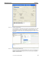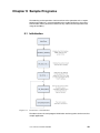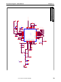
1
User's Manual
8-bit 78K0 ZigBee™
Development Platforms
Document No. U18849EE1V0UM00
Date published July 2007
© NEC Electronics 2007
Printed in Germany
Legal Notes
2
•
The information in this document is current as of xxxxx, 20xx.
The information is subject to change without notice. For actual
design-in, refer to the latest publications of NEC Electronics
data sheets or data books, etc., for the most up-to-date
specifications of NEC Electronics products. Not all products
and/or types are available in every country. Please check with
an NEC Electronics sales representative for availability and
additional information.
•
No part of this document may be copied or reproduced in any form
or by any means without the prior written consent of NEC
Electronics. NEC Electronics assumes no responsibility for any
errors that may appear in this document.
•
NEC Electronics does not assume any liability for infringement of
patents, copyrights or other intellectual property rights of third
parties by or arising from the use of NEC Electronics products listed
in this document or any other liability arising from the use of such
products. No license, express, implied or otherwise, is granted under
any patents, copyrights or other intellectual property rights of NEC
Electronics or others.
•
Descriptions of circuits, software and other related information in this
document are provided for illustrative purposes in semiconductor
product operation and application examples. The incorporation of
these circuits, software and information in the design of a customer's
equipment shall be done under the full responsibility of the customer.
NEC Electronics assumes no responsibility for any losses incurred
by customers or third parties arising from the use of these circuits,
software and information.
•
While NEC Electronics endeavors to enhance the quality, reliability
and safety of NEC Electronics products, customers agree and
acknowledge that the possibility of defects thereof cannot be
eliminated entirely. To minimize risks of damage to property or injury
(including death) to persons arising from defects in NEC Electronics
products, customers must incorporate sufficient safety measures in
their design, such as redundancy, fire-containment and anti-failure
features.
•
NEC Electronics products are classified into the following three
quality grades: "Standard", "Special" and "Specific".
•
The "Specific" quality grade applies only to NEC Electronics
products developed based on a customer-designated "quality
assurance program" for a specific application. The recommended
applications of an NEC Electronics product depend on its quality
grade, as indicated below. Customers must check the quality grade
of each NEC Electronics product before using it in a particular
application.
"Standard": Computers, office equipment, communications
equipment, test and measurement equipment, audio and visual
equipment, home electronic appliances, machine tools, personal
electronic equipment and industrial robots.
"Special": Transportation equipment (automobiles, trains, ships,
etc.), traffic control systems, anti-disaster systems, anti-crime
User's Manual U18849EE1V0UM00
systems, safety equipment and medical equipment (not specifically
designed for life support).
"Specific": Aircraft, aerospace equipment, submersible repeaters,
nuclear reactor control systems, life support systems and medical
equipment for life support, etc.
The quality grade of NEC Electronics products is "Standard" unless otherwise
expressly specified in NEC Electronics data sheets or data books, etc. If
customers wish to use NEC Electronics products in applications not intended by
NEC Electronics, they must contact an NEC Electronics sales representative in
advance to determine NEC Electronics' willingness to support a given application.
(Note)
(1) "NEC Electronics" as used in this statement means NEC Electronics
Corporation and also includes its majority-owned subsidiaries.
(2) "NEC Electronics products" means any product developed or manufactured
by or for NEC Electronics (as defined above).
User's Manual U18849EE1V0UM00
3
Regional Information
Some information contained in this document may vary from country to country. Before
using any NEC product in your application, please contact theNEC office in your country
to obtain a list of authorized representatives anddistributors. They will verify:
•
Device availability
•
Ordering information
•
Product release schedule
•
Availability of related technical literature
•
Development environment specifications (for example, specifications for
third-party tools and components, host computers, power plugs, AC
supply voltages, and so forth)
•
Network requirements
In addition, trademarks, registered trademarks, export restrictions, and otherlegal
issues may also vary from country to country.
NEC Electronics Corporation
1753, Shimonumabe, Nakahara-ku,
Kawasaki, Kanagawa 211-8668, Japan
Tel: 044 4355111
http://www.necel.com/
[America]
[Europe]
[Asia & Oceania]
NEC Electronics America, Inc.
2880 Scott Blvd.
Santa Clara, CA 95050-2554,
U.S.A.
Tel: 408 5886000
http://www.am.necel.com/
NEC Electronics (Europe) GmbH
Arcadiastrasse 10
40472 Düsseldorf, Germany
Tel: 0211 65030
http://www.eu.necel.com/
NEC Electronics (China) Co., Ltd
7th Floor, Quantum Plaza, No. 27
ZhiChunLu Haidian District,
Beijing 100083, P.R.China
Tel: 010 82351155
http://www.cn.necel.com/
United Kingdom Branch
Cygnus House, Sunrise Parkway
Linford Wood, Milton Keynes
MK14 6NP, U.K.
Tel: 01908 691133
Succursale Française
9, rue Paul Dautier, B.P. 52
78142 Velizy-Villacoublay Cédex
France
Tel: 01 30675800
Sucursal en España
Juan Esplandiu, 15
28007 Madrid, Spain
Tel: 091 5042787
Tyskland Filial
Täby Centrum
Entrance S (7th floor)
18322 Täby, Sweden
Tel: 08 6387200
4
NEC Electronics Shanghai Ltd.
Room 2511-2512, Bank of China
Tower,
200 Yincheng Road Central,
Pudong New Area,
Shanghai 200120, P.R. China
Tel: 021 58885400
http://www.cn.necel.com/
NEC Electronics Hong Kong Ltd.
12/F., Cityplaza 4,
12 Taikoo Wan Road, Hong Kong
Tel: 2886 9318
http://www.hk.necel.com/
NEC Electronics Taiwan Ltd.
7F, No. 363 Fu Shing North Road
Taipei, Taiwan, R.O.C.
Tel: 02 27192377
Filiale Italiana
Via Fabio Filzi, 25/A
20124 Milano, Italy
Tel: 02 667541
NEC Electronics Singapore Pte. Ltd.
238A Thomson Road,
#12-08 Novena Square,
Singapore 307684
Tel: 6253 8311
http://www.sg.necel.com/
Branch The Netherlands
Steijgerweg 6
5616 HS Eindhoven,
The Netherlands
Tel: 040 2654010
NEC Electronics Korea Ltd.
11F., Samik Lavied’or Bldg., 720-2,
Yeoksam-Dong, Kangnam-Ku, Seoul,
135-080, Korea Tel: 02-558-3737
http://www.kr.necel.com/
User's Manual U18849EE1V0UM00
Table of Contents
Chapter 1
78K0 ZigBee Development Solutions . . . . . . . . . . . . . . . . . . . . .
7
1.1
TK-78K0/KF2+UZ . . . . . . . . . . . . . . . . . . . . . . . . . . . . . . . . . . . . . . . . . . . . . . . . . . . . . . . . . . . . . . . . . 7
1.2
Features . . . . . . . . . . . . . . . . . . . . . . . . . . . . . . . . . . . . . . . . . . . . . . . . . . . . . . . . . . . . . . . . . . . . . . . . . . 7
1.3
System Requirements . . . . . . . . . . . . . . . . . . . . . . . . . . . . . . . . . . . . . . . . . . . . . . . . . . . . . . . . . . . . . 7
1.4
System Configuration . . . . . . . . . . . . . . . . . . . . . . . . . . . . . . . . . . . . . . . . . . . . . . . . . . . . . . . . . . . . . 8
1.5
78K0 ZigBee™ Development Platforms . . . . . . . . . . . . . . . . . . . . . . . . . . . . . . . . . . . . . . . . . . . . .
1.5.1
ZigBee™ Starter Kit . . . . . . . . . . . . . . . . . . . . . . . . . . . . . . . . . . . . . . . . . . . . . . . . . . . . . . .
1.5.2
ZigBee™ Professional Developers Kit . . . . . . . . . . . . . . . . . . . . . . . . . . . . . . . . . . . . . . .
1.5.3
ZigBee™ Premium Developers Kit . . . . . . . . . . . . . . . . . . . . . . . . . . . . . . . . . . . . . . . . . .
Chapter 2
Sample Program Overview . . . . . . . . . . . . . . . . . . . . . . . . . . . . . . . . . . .
8
8
9
9
10
2.1
RF Test Program . . . . . . . . . . . . . . . . . . . . . . . . . . . . . . . . . . . . . . . . . . . . . . . . . . . . . . . . . . . . . . . . . . 10
2.2
Sample Program 1 - Wireless Text Chat . . . . . . . . . . . . . . . . . . . . . . . . . . . . . . . . . . . . . . . . . . . . 10
2.3
Sample Program 2 - LED Test Using a Star Network . . . . . . . . . . . . . . . . . . . . . . . . . . . . . . . . . 11
2.4
Programming the Nodes with the Sample Programs . . . . . . . . . . . . . . . . . . . . . . . . . . . . . . . . . 12
Chapter 3
Hardware Specification TK-78K0/KF2+UZ . . . . . . . . . . . . . .
16
3.1
Terminal List . . . . . . . . . . . . . . . . . . . . . . . . . . . . . . . . . . . . . . . . . . . . . . . . . . . . . . . . . . . . . . . . . . . . . . 16
3.2
Switches and LEDs . . . . . . . . . . . . . . . . . . . . . . . . . . . . . . . . . . . . . . . . . . . . . . . . . . . . . . . . . . . . . . . .
3.2.1
SW1, SW5, JP1 . . . . . . . . . . . . . . . . . . . . . . . . . . . . . . . . . . . . . . . . . . . . . . . . . . . . . . . . . . .
3.2.2
Flash Programming Mode . . . . . . . . . . . . . . . . . . . . . . . . . . . . . . . . . . . . . . . . . . . . . . . . . .
3.2.3
On-chip Debug Mode . . . . . . . . . . . . . . . . . . . . . . . . . . . . . . . . . . . . . . . . . . . . . . . . . . . . . .
3.2.4
Normal Operation Mode . . . . . . . . . . . . . . . . . . . . . . . . . . . . . . . . . . . . . . . . . . . . . . . . . . .
3.2.5
General Purpose Port Setting . . . . . . . . . . . . . . . . . . . . . . . . . . . . . . . . . . . . . . . . . . . . . . .
3.3
SW2 . . . . . . . . . . . . . . . . . . . . . . . . . . . . . . . . . . . . . . . . . . . . . . . . . . . . . . . . . . . . . . . . . . . . . . . . . . . . . . 20
3.4
SW3, SW4 . . . . . . . . . . . . . . . . . . . . . . . . . . . . . . . . . . . . . . . . . . . . . . . . . . . . . . . . . . . . . . . . . . . . . . . . 21
3.5
LED2, LED3 and LED4 . . . . . . . . . . . . . . . . . . . . . . . . . . . . . . . . . . . . . . . . . . . . . . . . . . . . . . . . . . . . . 22
3.6
Power Supply . . . . . . . . . . . . . . . . . . . . . . . . . . . . . . . . . . . . . . . . . . . . . . . . . . . . . . . . . . . . . . . . . . . . . 22
Chapter 4
TK-78K0/KF2+UZ Data
18
18
18
19
19
20
. . . . . . . . . . . . . . . . . . . . . . . . . . . . . . . . . . . . . . . . 24
4.1
Parts Layout . . . . . . . . . . . . . . . . . . . . . . . . . . . . . . . . . . . . . . . . . . . . . . . . . . . . . . . . . . . . . . . . . . . . . . 24
4.2
RF Board Connection Figure . . . . . . . . . . . . . . . . . . . . . . . . . . . . . . . . . . . . . . . . . . . . . . . . . . . . . . . 25
Chapter 5
Hardware Installation 78K0 UZ Stick
. . . . . . . . . . . . . . . . . . . . . 26
5.1
Hardware Overview . . . . . . . . . . . . . . . . . . . . . . . . . . . . . . . . . . . . . . . . . . . . . . . . . . . . . . . . . . . . . . . 26
5.2
Block Diagram . . . . . . . . . . . . . . . . . . . . . . . . . . . . . . . . . . . . . . . . . . . . . . . . . . . . . . . . . . . . . . . . . . . . 27
Chapter 6
Switches and LEDs
. . . . . . . . . . . . . . . . . . . . . . . . . . . . . . . . . . . . . . . . . . . . . 29
6.1
SW1 - FLMD0 . . . . . . . . . . . . . . . . . . . . . . . . . . . . . . . . . . . . . . . . . . . . . . . . . . . . . . . . . . . . . . . . . . . . . 29
6.2
SW2 - Power . . . . . . . . . . . . . . . . . . . . . . . . . . . . . . . . . . . . . . . . . . . . . . . . . . . . . . . . . . . . . . . . . . . . . . 29
6.3
LED1 - Power Indication . . . . . . . . . . . . . . . . . . . . . . . . . . . . . . . . . . . . . . . . . . . . . . . . . . . . . . . . . . . 29
6.4
LED2, LED3 and LED4 . . . . . . . . . . . . . . . . . . . . . . . . . . . . . . . . . . . . . . . . . . . . . . . . . . . . . . . . . . . . . 30
Chapter 7
7.1
ZigBee™ Development Platforms, Installation and
Operation . . . . . . . . . . . . . . . . . . . . . . . . . . . . . . . . . . . . . . . . . . . . . . . . . . . . . . . . . . . 31
Hardware Installation . . . . . . . . . . . . . . . . . . . . . . . . . . . . . . . . . . . . . . . . . . . . . . . . . . . . . . . . . . . . . . 31
User's Manual U18849EE1V0UM00
5
7.2
Software Installation . . . . . . . . . . . . . . . . . . . . . . . . . . . . . . . . . . . . . . . . . . . . . . . . . . . . . . . . . . . . . . 31
7.3
Sample Program Installation . . . . . . . . . . . . . . . . . . . . . . . . . . . . . . . . . . . . . . . . . . . . . . . . . . . . . . . 31
7.4
USB Driver Installation . . . . . . . . . . . . . . . . . . . . . . . . . . . . . . . . . . . . . . . . . . . . . . . . . . . . . . . . . . . . 32
7.4.1
Installation on Windows 2000 . . . . . . . . . . . . . . . . . . . . . . . . . . . . . . . . . . . . . . . . . . . . . . . 32
7.4.2
Installation on Windows XP . . . . . . . . . . . . . . . . . . . . . . . . . . . . . . . . . . . . . . . . . . . . . . . . . 38
Chapter 8
IAR Sample Session
. . . . . . . . . . . . . . . . . . . . . . . . . . . . . . . . . . . . . . . . . . . . 44
8.1
Project Loading . . . . . . . . . . . . . . . . . . . . . . . . . . . . . . . . . . . . . . . . . . . . . . . . . . . . . . . . . . . . . . . . . . . 44
8.2
Option Setting . . . . . . . . . . . . . . . . . . . . . . . . . . . . . . . . . . . . . . . . . . . . . . . . . . . . . . . . . . . . . . . . . . . . 45
8.3
Debugging . . . . . . . . . . . . . . . . . . . . . . . . . . . . . . . . . . . . . . . . . . . . . . . . . . . . . . . . . . . . . . . . . . . . . . . . 46
Chapter 9
Sample Programs
. . . . . . . . . . . . . . . . . . . . . . . . . . . . . . . . . . . . . . . . . . . . . . . 49
9.1
Initialisation . . . . . . . . . . . . . . . . . . . . . . . . . . . . . . . . . . . . . . . . . . . . . . . . . . . . . . . . . . . . . . . . . . . . . . 49
9.2
Servicing the SK_LAYER_API . . . . . . . . . . . . . . . . . . . . . . . . . . . . . . . . . . . . . . . . . . . . . . . . . . . . . . 50
9.3
Managing and Actioning the User Interface . . . . . . . . . . . . . . . . . . . . . . . . . . . . . . . . . . . . . . . . . 51
Chapter 10 Schematic Diagrams TK-78K0/KF2-UZ . . . . . . . . . . . . . . . . . .
10.1
Circuit Diagram of UZ2400 RF board . . . . . . . . . . . . . . . . . . . . . . . . . . . . . . . . . . . . . . . . . . . . . . . 56
Chapter 11 Schematic Diagrams 78K0 UZ Stick
6
53
User's Manual U18849EE1V0UM00
. . . . . . . . . . . . . . . . . . . . . . 57
Chapter 1 78K0 ZigBee Development Solutions
1.1 TK-78K0/KF2+UZ
The TK-78K0/KF2+UZ is the NEC Electronics 8-bit starter kit specifically designed
for the development of wireless networking applications. The above platform can
be used to design and develop a broad range of wireless networks from simple
peer to peer to full mesh networking incorporating all of the features of a fully
compliant ZigBee™ network.
1.2 Features
Features of the TK-78K0/KF2+UZ MCU board are as follows.
•
•
•
•
•
•
•
•
•
•
•
The evaluation board uses the NEC Electronics 8-bit single chip
microcontroller (μPD78F0547D).
All of ROM, RAM and a multitude of peripherals are efficiently built
in one chip on a single board.
High-speed operation with a16 MHz clock.
Sub-clock 32.768 KHz standard equipment
128 Kbytes Flash memory is built into MCU chip.
A high-speed RAM:1024 Bytes and an additional 6144 Bytes of RAM.
Hardware is ready to accommodate 2.4GHz transceiver chip
UZ2400 (IEEE802.15.4 ZigBee™ compliant wireless personal area
network) made by Uniband Electronic Corporation
http://www.ubec.com.tw/index.html
Attached antenna Titanis made by Gigaant
http://www.gigaant.com/
A maximum of 17 I/O ports are used, with an on-board temperature
sensor for applications development. (S-8120C made by SII
http://www.sii.co.jp/)
Debugging using the on-board on-chip debug function can be.
USB or battery powered with a compact form factor of 70 mm × 60
mm.
Please inquire direct to the parts maker about specification of UZ2400 chip,
antenna and temperature sensor.
1.3 System Requirements
Host PC
Host Interface
A PC supporting Windows 2000 or Windows XP for the IAR Systems Embedded
Workbench Kickstart edition and the 78K0 ZigBee™ development platforms.
Pentium 200 MHz minimum, 128 MB of RAM, 256 colour display (1024 x 768),
mouse, CD ROM drive and 200 Mbytes of disk space are required to install the
tool packages.
USB interface that enables communication based on USB (Version 1.1 or later).
User's Manual U18849EE1V0UM00
7
Chapter 1
78K0 ZigBee Development Solutions
Package Contents
Please verify that you have received all of the parts listed in the package contents
list attached to the 78K0 ZigBee™ platforms (varies with development platform
purchased). If any parts are missing or seem to be damaged please contact the
dealer from whom you received your 78K0 ZigBee™ development platform.
Note
Updates for the IAR Embedded workbench for 78K, documentation and/or
utilities for the 78K0 ZigBee™ platforms if available maybe downloaded from the
NEC Electronics web pages at: http://www.eu.necel.com/updates
Trademarks
IAR Embedded Workbench, visualSTATE, IAR MakeApp and C-SPY are
registered trademarks of IAR Systems AB. Microsoft and Windows are registered
trademarks of Microsoft Corporation. Adobe and Acrobat Reader are registered
trademarks of Adobe Systems Incorporated.
All other product names are trademarks or registered trademarks of their
respective owners.
1.4 System Configuration
Figure 1-1
System Connection
1.5 78K0 ZigBee™ Development Platforms
There are 3 variants of the 78K0 ZigBee™ Development platforms.
1.5.1 ZigBee™ Starter Kit
This starter kit consists of 2 78K0/KF2+UZ development boards and the IAR
software development tools. Also provided are the IEEE 802.15.4 MAC libraries
in both banked and non-banked form. The following sample applications are
provided:
RF Test program.
Sample 1 Wireless text chat program.
Sample2 Led test using a star network
8
User's Manual U18849EE1V0UM00
78K0 ZigBee Development Solutions
Chapter 1
1.5.2 ZigBee™ Professional Developers Kit
The professional developers kit consists of 4 78K0/KF2+UZ development boards
and the IAR software development tools. Also provided are the IEEE 802.15.4
MAC libraries in both banked and non-banked form. The following sample
applications are provided:
RF Test program.
Sample 1 Wireless text chat program.
Sample2 Led test using a star network
Also included in the professional developers kit are the following aids for
developing full ZigBee™ wireless networks.
30 day software security dongle for the ZigBee™ stack and ZigBee™ Software
Developers kit.
Link to secure website for downloading ZigBee™ and SDK.
Flash programming files to allow one of the boards to be utilised as an Air Sniffer
(in conjunction with software supplied in the SDK).
1.5.3 ZigBee™ Premium Developers Kit
The premium developers kit consists of 4 78K0/KF2+UZ development boards, 1
78K0 UZ stick and the IAR software development tools. Also provided are the
IEEE 802.15.4 MAC libraries in both banked and non-banked form. The following
sample applications are provided:
RF Test program.
Sample 1 Wireless text chat program.
Sample2 Led test using a star network
Also included in the professional developers kit are the following aids for
developing full ZigBee™ wireless networks.
Unlimited software security dongle for the ZigBee™ stack and ZigBee™ Software
Developers kit.
Link to secure website for downloading ZigBee™ and SDK.
Flash programming files to allow one of the boards to be utilised as an Air Sniffer
(in conjunction with software supplied in the SDK).
User's Manual U18849EE1V0UM00
9
Chapter 2 Sample Program Overview
2.1 RF Test Program
The RF test program is a simple program that allows various RF parameters to be
configured and test signals generated. The features found in this program can be
used to provide the software support functions needed for various test
requirements.
In the sample provided a simple terminal program like “Hyperterminal” is required
to select the relevant mode of operation. For all “Hyperterminal” please use the
following settings and relevant serial port.
Baud Rate
Data bits
Parity
Stop bits
Flow control
Figure 2-1
19200
8
N
1
None
RF Test Menu
As can be seen from the above multiple test modes are available via simple single
key operation.
2.2 Sample Program 1 - Wireless Text Chat
In this sample program it is possible to configure 2 or more nodes for a wireless
conversation using text.
10
User's Manual U18849EE1V0UM00
Sample Program Overview
Chapter 2
To demonstrate this program you will again need a simple terminal emulation
program like “Hyperterminal” connected to each node on the network.
Figure 2-2
RF Test Demonstration
In the above demonstration 1 node is configured as a coordinator and the other
nodes associate to this node, when association is complete you send messages
between nodes by specifying the short address and text data.
2.3 Sample Program 2 - LED Test Using a Star Network
In this sample program 2 or nodes can form a star network ( a star network has a
central coordinator with several nodes connecting to the coordinator only).
Figure 2-3
Star Network Configuration
To enable 1 module to be the coordinator it necessary to set dip switch SW1
switch 8 to the on position. It is necessary to power cycle the unit or reset the unit
as the SW1 switch 8 is only read following a reset.
User's Manual U18849EE1V0UM00
11
Chapter 2
Sample Program Overview
You must only enable one module to be the coordinator on the network all other
modules must be end devices so please ensure that all of the other modules have
SW1 switch 8 set to the off position.
To ensure that each end device that joins the network reliably it is necessary to
associate on to the network with a different network address for each end device.
This is achieved by the following process.
Press the reset switch (SW6) and any of the switch positions of the directional
switch (SW2).
Release the reset switch (SW6).
Wait 1 second and then release the directional switch (SW2).
The nodes will then associate to the coordinator and form a star network.
The following table shows how the addresses are allocated depending upon the
selection of SW2 following a reset.
Table 2-1
SW2 Address Selection
SW2 Up Position Selected
Default Address + 1
SW2 Centre Position Selected
Default Address + 2
SW2 Left Position Selected
Default Address + 3
SW2 Right Position Selected
Default Address + 4
SW2 Down Position Selected
Default Address + 5
When association is complete pressing SW3 on the end devices will cause LED2
to flash on the coordinator and pressing SW4 on the end devices will cause LED3
to flash on the coordinator.
Note! if SW2 is not active following a reset then all end devices will try and
associate using the default address.
It is also possible to connect “Hyperterminal” to the development boards and view
the association and data transfer as text messages.
2.4 Programming the Nodes with the Sample Programs
The 78K0/KF2-UZ boards will come pre-programmed with the text chat sample
application, in order to demonstrate the additional applications it is required to
use the flash programming software supplied.
After installation the PG-FPL3 can be launched from the NEC Tools32 program
group. The following screen will appear.
12
User's Manual U18849EE1V0UM00
Sample Program Overview
Figure 2-4
Chapter 2
PG-FPL3 Main Screen
It is vital to ensure that the correct device parameter file is loaded for the TK-78K0/
KF2+UZ board you must select the 78F0547D.PRM file and for the 78K0 UZ Stick
you must select the 78F0537D.PRM file.
To select the correct device file click the setup button and the following dialog will
appear.
Figure 2-5
PG-FPL3 Setup Screen
User's Manual U18849EE1V0UM00
13
Chapter 2
Sample Program Overview
Select PRM File Read and choose the correct device file for the relevant hardware.
While this dialog is open you can also select the com port that the target is
connected to and change the clock frequency to 16.00 MHz (the operating
frequency of the 78K0 ZigBee™ development platforms).
The sample programs for the TK-78K0/KF2+UZ and the 78K0 UZ Stick are
available in both normal configuration and memory banked configuration, the
default location for the sample programs is \TK78K0\SamplePrograms\.
To load a sample program select the file load button the following dialog will
appear.
Figure 2-6
PG-FPL3 File Load
Using the drop down list box you can select the relevant sample program.
Figure 2-7
PG-FPL3 Select Directory
When the relevant file is loaded you are now ready to re-program the target
hardware. To program the hardware first ensure that the unit is configured in flash
programming mode (see chapter x) and also ensure that the unit is plugged in to
the USB port and the correct COM port assignment is set.
14
User's Manual U18849EE1V0UM00
Sample Program Overview
Chapter 2
The easiest way to program the unit is to select the auto button this will
automatically erase, program and verify that the device has been re-programmed
successfully. The following shows the programming screen.
Figure 2-8
PG-FPL3 Flash Programming
You are now ready to test the relevant sample application.
User's Manual U18849EE1V0UM00
15
Chapter 3 Hardware Specification TK-78K0/KF2
+UZ
MCU
Operation frequency
RF transceiver
Interface
Operation voltage
μPD78F0547DGK
16 MHz Operation (Sub-clock:32.768 KHz)
UZ2400 RF Board
USB (Mini B connector)
RF board connector
Connector of board in surrounding (CN1: not mounted)
Connector of battery (9.0 V - 6.5 V)
5.0 V (Supply from USB)
9.0 V (Supply from a battery, Min.6.5 V)
3.1 Terminal List
Terminal tables of CN1, CN3 and CN4 of TK-78K0/KF2+UZ MCU board.
CN1 terminal list (FFC-20BMEP1 [not mounted] by HONDA CONNECTORS)
Table 3-1
16
CN1
CN1
Signal
name
Terminal MCU name at
connection destination
Notes
1
VDD
VDD
+3.3V
2
P10
P10/SCK10/TxD0
3
P11
P11/SI10/RxD0
4
P12
P12/SO10
5
P15
P15/TOH0
6
P16
P16/TOH1/INTP5
7
P17
P17/TI50/TO50
8
P24
P24/ANI4
9
P25
P25/ANI5
10
P26
P26/ANI6
11
P27
P27/ANI7
12
P33
P33/TI51/TO51/INTP4
13
P60
P60/SCL0
14
P61
P61/SDA0
15
P62
P62/EXSCL0
16
P120
P120/INTP0/EXLVI
17
GND
GND
18
P140
P140/PCL/INTP6
19
GND
GND
20
P141
P141/BUZ/BUSY0/INTP7
User's Manual U18849EE1V0UM00
Hardware Specification TK-78K0/KF2+UZ
Figure 3-1
Chapter 3
Pin 20
Pin 19
Pin 2
Pin 1
CN1 Pin Configuration
CN3 terminal list (TFM-110-02-S-D-A-K-TR [not mounted by SAMTEC])
Table 3-2
CN3
CN3
Signal
name
Terminal MCU name
1
GND
GND
2
3
Notes
N.C.
VREG_EN
P50
4
Output from MCU
N.C.
5
RESn
P51
Output from MCU
6
FIFO
P33/TI51/TO50/INTP4
Input to MCU
FIFOP
P52
7
8
N.C.
9
10
N.C.
CCA
P53
11
12
SFD
P06/TI011/TO01
Input to MCU
N.C.
CSn
P43
15
16
Input to MCU
N.C.
13
14
Input to MCU
Output from MCU
N.C.
SCLK
P04/SCK11
17
Output from MCU
N.C.
18
SI
P02/SO11
19
GND
GND
20
SO
P03/SI11
Output from MCU
Input to MCU
CN4 terminal list (TFM-110-02-S-D-A-K-TR [not mounted by SAMTEC])
Table 3-3
CN4
CN4
Signal
name
1
TP2
2
GND
3
TP2
4
GND
5
TP2
Terminal MCU name
Notes
GND
GND
User's Manual U18849EE1V0UM00
17
Chapter 3
Hardware Specification TK-78K0/KF2+UZ
CN4
Signal
name
Terminal MCU name
6
GND
GND
7
3.3V
8
GND
9
3.3V
10
GND
11
TP3
12
GND
13
TP4
14
GND
GND
GND
GND
GND
15
16
N.C.
GND
GND
17
18
N.C.
GND
GND
19
20
N.C.
GND
GND
CN3
Figure 3-2
Notes
Pin1
Pin2
Pin19
Pin20
CN4
Pin1
Pin2
Pin19
Pin20
CN3 - CN4
3.2 Switches and LEDs
3.2.1 SW1, SW5, JP1
Bits 1-5 of SW1 is a Dip switch that is used to set the operational mode.
SW5 is a slide switch to select an operation mode.
JP1 is a jumper to select a power source.
3.2.2 Flash Programming Mode
Flash EEPROM on the 78K0/KF2+ZB MCU can be programmed using the
attached software “PG-FPL3” in your PC, which is connected to the MCU board
via USB cable, if the following switch and jumper setting is made.
18
User's Manual U18849EE1V0UM00
Hardware Specification TK-78K0/KF2+UZ
Table 3-4
Flash Programming Mode
SW1
Figure 3-3
Chapter 3
Bit 1
ON
Bit 2
ON
Bit 3
OFF
Bit 4
OFF
Bit 5
OFF
SW5
UART
JP1
USB (1-2pin short)
Configuration Switches
3.2.3 On-chip Debug Mode
The following setting activates the On-chip debug functions on the MCU.
Table 3-5
On-chip Debug Mode
SW1
Bit 1
ON
Bit 2
ON
Bit 3
ON
Bit 4
ON
Bit 5
ON
SW5
OCD
JP1
USB (1-2pin short)
3.2.4 Normal Operation Mode
Please change to the following settings when you execute the program normally.
Table 3-6
Normal Operation Mode Settings
SW1
Bit 1
OFF
Bit 2
OFF
Bit 3
OFF
User's Manual U18849EE1V0UM00
19
Chapter 3
Hardware Specification TK-78K0/KF2+UZ
Bit 4
OFF
Bit 5
OFF
SW5
UART
JP1
see below
Selection of power source by JP1
Table 3-7
Power Source Selection
USB Power
USB (1-2pin short)
Battery
CN2 (2-3pin short)
3.2.5 General Purpose Port Setting
Bits 6-8 of SW1 are connected to general purpose I/O ports.
If the relative switch is active then the I/O port is pulled low, if the switch is open
then turn on pull-up resistor (PU0).
For more detail of the pull-up resistor, please refer to the User’s manual of the
μPD78F0547 MCU.
Table 3-8
General Purpose Switch Setting
SW1
Signal name
Terminal MCU
Name
Bit 6
P00
P00/TI000
Bit 7
P01
P01/TI010/TO00
Bit 8
P05
P05/TI001/SSI11
Notes
3.3 SW2
SW2 is a 4 directional switch with a central push. If it is directed or pushed, the
relevant input is set to GND. Otherwise the circuit is open. Therefore set the onchip pull-up resistors (PU7) during initializing routine of your program code.
For more detail, please refer to the User’s manual of the μPD78F0547 MCU.
SW2 terminal list (ALPS SKRHADE010)
Table 3-9
20
SW2 Selection
SW2
Signal name
Terminal MCU
name
Notes
1
P72
P72/KR2
UP
2
P73
P73/KR3
CENTER PUSH
3
P74
P74/KR4
LEFT
4
P75
P75/KR5
RIGHT
5
GND
GND
6
P76
P76/KR6
User's Manual U18849EE1V0UM00
DOWN
Hardware Specification TK-78K0/KF2+UZ
Figure 3-4
Chapter 3
SW2 Directional Switch
3.4 SW3, SW4
SW3 and SW4 are tact switches. The port inputs are short-circuited to ground,
while they are being pushed, and kept open otherwise. Therefore set the on-chip
pull-up resistors(PU7) during initializing routine of your program code.
For more detail, please refer to the User’s manual of the μPD78F0547 MCU.
SW3 and SW4 terminal list (ALPS SKQMBBE010)
Table 3-10
Figure 3-5
Sw3 and SW4 Settings
Signal name
Terminal MCU
name
SW3
P70
P70/KR0
SW4
P71
P71/KR1
Notes
SW3 and SW4
SW6 is the reset switch. MCU can be reset by pushing this switch.
User's Manual U18849EE1V0UM00
21
Chapter 3
Hardware Specification TK-78K0/KF2+UZ
Figure 3-6
SW6 Reset Switch
'Power LED'. LED1 is activated when the power supply is turned on.
Figure 3-7
Power LED
3.5 LED2, LED3 and LED4
LED2, LED3, and LED4 are available for applications. To turn the LED on, please
set the relevant output port LOW.
LED2, LED3 and LED4 Terminal list (STANLEY ELECTRIC PG1111C)
Table 3-11
Figure 3-8
LED Setting
Signal name
Terminal MCU
name
LED2
P40
P40
LED3
P41
P41
LED4
P42
P42
Notes
LED Identification
3.6 Power Supply
There are two choices to supply power to the board, USB or a 006P battery via
CN2. Please refer to 2.1.3 JP1 for the jumper setting.
Please replace the battery with a new one, if the voltage level goes down to 6.5
V.
22
User's Manual U18849EE1V0UM00
Hardware Specification TK-78K0/KF2+UZ
Chapter 3
Below the voltage level of 6.5V, functions of the board are not guaranteed.
The battery voltage can be checked at the port as shown below.
Table 3-12
Battery Monitoring
Signal Name
BT_MONI
Terminal MCU
name at
connection
destination
Notes
P20/ANI0
33.8% of the battery output is available at ANI0.
For instance, If the battery level is 9 V,
the level of the BT_MONI
= 0.338 × 9.0 V = 3.042 V
If the battery level is 6.5 V,
the level of the BT_MONI
= 0.338 × 6.5 V = 2.197 V
User's Manual U18849EE1V0UM00
23
Chapter 4 TK-78K0/KF2+UZ Data
4.1 Parts Layout
Figure 4-1
24
TK-78K0/KF2 Parts Layout
User's Manual U18849EE1V0UM00
TK-78K0/KF2+UZ Data
Chapter 4
4.2 RF Board Connection Figure
Figure 4-2
RF Connection
User's Manual U18849EE1V0UM00
25
Chapter 5 Hardware Installation 78K0 UZ Stick
The 78K0 UZ stick is an additional module based on the NEC 78K0/KE2
microcontroller. This module can be used as either a network node or a dedicated
hardware module for interfacing to the Air Sniffer application ( part of the ZigBee™
SDK) depending upon the flash program loaded on to the module.
Features of the 78K0 UZ stick include:
•
•
•
•
•
•
•
•
•
•
Hardware is ready to accommodate IEEE 802.15.4/ZigBee™
compliant wireless personal area network with 8 bit single chip MCU
78K0/KE2, μPD78F0537DGA, and 2.4 GHz transceiver UZ2400
Object code of IEEE 802.15.4 PHY/MAC is included in the kit and
possible to utilize as a library.
128 Kbytes of Flash EEPROM, available on chip in the 78K0/KE2
MCU, is programmable from PC via USB connection without any
additional Flash programming hardware. Flash programming utility,
PG-FPL3, which works on MS Windows in your PC, is included in
the kit.
Debugging of the program requires an optional connector,
SICA2P20S, an additional adaptor, SICA10I2P, and a MINICUBE
emulator, QB-78K0MINI or QB-MINI2.
USB connection can be utilized not only for Flash programming, but
also for user applications and power supply.
Real time clock is available on the board.
In addition to the USB connector, one serial I/O port, UART or CSI,
one interrupt input port, and three analogue input ports are available
in the expansion connector.
The expansion connector also provides with a connection to a 006P
battery. Power source can be selectable between USB or a battery
by a switch.
Three orange LEDs are available on board for applications, in
addition to one green LED for power indication.
The size of the module is 82 x 23 mm.
5.1 Hardware Overview
MCU
Clock
RF transceiver
Interfaces
Power supply
26
UD78F0537DGA with 128 KB Flash EEPROM and 7 KB
RAM
16MHz main, and 32.768KHz sub
UZ2400
USB connector (Type A)
Expansion interface
Option: MINICUBE connector (CN1)
5.0 V by USB, or 4.75 - 10.0 V by a battery
User's Manual U18849EE1V0UM00
Hardware Installation 78K0 UZ Stick
Chapter 5
5.2 Block Diagram
Figure 5-1
Block Diagram 78K0 UZ Stick
Interface Connection
CN1 Minicube/Minicube 2
Table 5-1
CN1 78K0 UZ Stick
CN1
Name
Connection to MCU Notes
1
RESET_IN
Pull-up with 10 K Ohm
2
REST_OUT
RESET
3
FLMD0
FLMD0
Programming Mode
4
VDD_IN
VDD (3.3V)
Regulated
5
X2
P32/INTP3/OCD1B
OCDX2
6
GND
GND
7
X1
P31/INTP2/OCD1A
8
GND
GND
9
-
N.C.
10
5V_CHK
N.C.
11
-
N.C.
12
-
N.C.
13
-
N.C.
14
-
N.C.
15
-
N.C.
16
-
N.C.
17
-
N.C.
18
-
N.C.
19
-
N.C.
20
-
N.C.
OCDX1
CN1: Tokyo Eletech SICA2P20S (Not fitted)
User's Manual U18849EE1V0UM00
27
Chapter 5
Hardware Installation 78K0 UZ Stick
Figure 5-2
Location of CN1
Expansion Interface: CN2
CN2: Hirose DF11-10DP-2DS
Table 5-2
CN2 78K0 UZ Stick
CN2
Name
Connection to MCU Notes
1
GND
GND
Battery GND
2
VBAT
4.75V - 10.0V
From battery
3
P10
P10/SCK10/TXD0
4
P11
P11/SI10/RXD0
5
P140
P140/PCL/INTP6
6
P12
P12/SO10
7
P24
P24/ANI4
8
P25
P25/ANI5
9
P26
P26/ANI6
10
GND
GND
Location of CN2: TOP VIEW
Figure 5-3
28
CN2 Location
User's Manual U18849EE1V0UM00
Chapter 6 Switches and LEDs
6.1 SW1 - FLMD0
Programming mode selection for Flash EEPROM on the MCU.
Setting of SW1: FLMD0
Figure 6-1
Normal Mode
L
Flash Programming Mode
H
SW1 Top View
6.2 SW2 - Power
Selection of power source: USB power or battery at CN2
Setting of SW2
Figure 6-2
USB Power
USB
CN2: Expansion I/F
BAT
SW2 Top View
6.3 LED1 - Power Indication
LED1 is a green LED to indicate the availability of power.
User's Manual U18849EE1V0UM00
29
Chapter 6
Switches and LEDs
LED1 status
Table 6-1
Figure 6-3
Power LED 78K0 UZ Stick
Status
LED
Power ON
Green
Power OFF
Off
LED1 Top View
6.4 LED2, LED3 and LED4
LED2, LED3, and LED4 are for application. They emit orange by setting the port
output of P40, P41, or P40 of the MCU low, respectively.
Table 6-2
LED Allocation 78K0 UZ Stick
Name
Figure 6-4
30
MCU Pin
Port Level
LED2 P40
P40/AD0
LOW for orange
HIGH for off
LED3 P41
P41/AD1
LOW for orange
HIGH for off
LED4 P42
P42/AD2
LOW for orange
HIGH for off
LED2, LED3, and LED4 Top View
User's Manual U18849EE1V0UM00
Chapter 7 ZigBee™ Development Platforms,
Installation and Operation
The IAR Embedded Workbench including the C-SPY debugger allows to build
and download application programs to the ZigBee™ development platforms!. As
communication interface between the PC host system and the ZigBee™
development platforms! board is USB, a USB interface line is needed. Before you
can download and run a program, software and hardware must be installed
properly.
CD ROM contents:
•
•
•
•
IAR Embedded Workbench for 78K0 Kickstart version
IEEE 802.15.4 MAC library
Sample Programs
Documentation
7.1 Hardware Installation
After unpacking ZigBee™ development platforms!, connect the board to your
host computer using the provided USB interface cable. When ZigBee™
development platforms! is connected, the USB driver needs to be installed on the
host machine. Please refer to the following section.
7.2 Software Installation
The ZigBee™ development platforms! package comes with the following software
demo packages:
•
•
IAR Systems Embedded Workbench for 78K0/78K0S/78K0R,
including C compiler, assembler, linker, librarian and IAR C-SPY
debugger / simulator
Sample programs
The IAR Systems Embedded Workbench must be installed on your PC. For
detailed installation hints, refer to the following chapters and to the corresponding
documentation of the IAR Embedded Workbench.
IAR Systems Embedded Workbench for 78K0/78K0S/78K0R installation
To install the IAR Systems Embedded Workbench for 78K0/K0S/K0R including
C-SPY debugger / simulator, select the SETUP program in the directory \IAR
Embedded Workbench 78K\ew78k\ of the CDROM. The setup dialogues will
guide you through the installation process.
7.3 Sample Program Installation
To install the sample/demonstration program for the ZigBee™ development
platforms! board select the SETUP program in the directory \TK78K0
User's Manual U18849EE1V0UM00
31
Chapter 7
ZigBee⢠Development Platforms, Installation and
Operation
\SamplePrograms\ of the CDROM. The setup dialogues will guide you through
the installation process.
7.4 USB Driver Installation
In order to use the ZigBee™ development platforms! board for On-Chip
debugging or FLASH programming, the USB driver needs to be installed on the
host machine. Install the driver according to the following procedure:
•
•
Installation on Windows 2000
Installation on Windows XP
7.4.1 Installation on Windows 2000
When the ZigBee™ development platforms! board is connected with the host
machine, the board is recognized by Plug and Play, and the wizard for finding new
hardware is started. Click Next >
Figure 7-1
Found New Hardware Wizard (Widows 2000)
The window below is displayed. So, check that "Search for a suitable driver ..." is
selected, then click Next >
32
User's Manual U18849EE1V0UM00
ZigBee⢠Development Platforms, Installation and
Operation
Figure 7-2
Chapter 7
Search Method (Windows 2000)
Check the "Specify a location" check box only, then click Next >
Figure 7-3
Driver File Location (Windows 2000)
Enter "C:\Program Files\NECTools32\FPL3\DRIVER" in the address bar, then
click OK.
User's Manual U18849EE1V0UM00
33
Chapter 7
ZigBee⢠Development Platforms, Installation and
Operation
Figure 7-4
Remark
Figure 7-5
Address Location 1 (Windows 2000)
As the installation destination folder enter "new-folder\FPL3\DRIVER". Click Next
>
File Location 1 (Windows 2000)
Click Finish to complete the installation of the USB driver.
34
User's Manual U18849EE1V0UM00
ZigBee⢠Development Platforms, Installation and
Operation
Figure 7-6
Chapter 7
USB Driver Installation Complete 1 (Windows 2000)
Proceed to the installation of the USB Serial Port driver. Click Next >
Figure 7-7
Found new Hardware Wizard 2 (Windows 2000)
The window below is displayed. So, check that "Search for a suitable driver ..." is
selected, then click Next >
User's Manual U18849EE1V0UM00
35
Chapter 7
ZigBee⢠Development Platforms, Installation and
Operation
Figure 7-8
Search Method 2 (Windows 2000)
Check the "Specify a location" check box only, then click Next >
Figure 7-9
Driver File Location 2 (Windows 2000)
Enter "C:\Program Files\NECTools32\FPL3\DRIVER" in the address bar, then
click OK.
36
User's Manual U18849EE1V0UM00
ZigBee⢠Development Platforms, Installation and
Operation
Figure 7-10
Remark
Figure 7-11
Chapter 7
Address Specification 2 (Windows 2000)
If the installation destination folder is changed at the time of GUI software
installation, enter "new-folder\DRIVER". Click Next >
Driver File Search 2 (Windows 2000)
Click Finish to complete the installation of the USB driver.
User's Manual U18849EE1V0UM00
37
Chapter 7
ZigBee⢠Development Platforms, Installation and
Operation
Figure 7-12
USB Driver Complete 2 (Windows 2000)
7.4.2 Installation on Windows XP
When the ZigBee™ development platforms! board is connected with the host
machine, the board is recognized by Plug and Play, and the wizard for finding new
hardware is started. Check that "Install from a list or specific ..." is selected, then
click Next >
38
User's Manual U18849EE1V0UM00
ZigBee⢠Development Platforms, Installation and
Operation
Figure 7-13
Chapter 7
Found New Hardware Wizard 1 (Windows XP)
Check that "Search for the best driver in these locations." is selected. Check the
"Include this location in the search:" check box and enter "C:\Program Files
\NECTools32\FPL3\DRIVER" in the address bar, then click Next >
Figure 7-14
Search Location 1 (Windows XP)
As shown below, "has not passed Windows Logo testing to verify its compatibility
with Windows XP." is displayed. Click Continue anyway.
User's Manual U18849EE1V0UM00
39
Chapter 7
ZigBee⢠Development Platforms, Installation and
Operation
Figure 7-15
Windows XP Logo Testing 1 (Windows XP)
When the window below is displayed, the installation of the USB driver is
completed. Click Finish.
Figure 7-16
USB Driver Installation Complete 1 (Windows XP)
Proceed to the installation of the USB Serial Port driver. Click Next >
Figure 7-17
40
Found New Hardware Wizard 2 (Windows XP)
User's Manual U18849EE1V0UM00
ZigBee⢠Development Platforms, Installation and
Operation
Chapter 7
Check that "Search for the best driver in these locations." is selected. Check the
"Include this location in the search:" check box and enter "C:\Program Files
\NECTools32\FPL3\DRIVER", then click Next >
Figure 7-18
Search Path 2 (Windows XP)
As shown below, "has not passed Windows Logo testing to verify its compatibility
with Windows XP." is displayed. Click Continue anyway.
Figure 7-19
Windows XP Logo Testing 2 (Windows XP)
User's Manual U18849EE1V0UM00
41
Chapter 7
ZigBee⢠Development Platforms, Installation and
Operation
When the window below is displayed, the installation of the USB driver is
completed. Click Finish.
Figure 7-20
Hardware Installation Wizard Complete 2 (Windows XP)
Confirmation of USB Driver Installation
After installing the two types of drivers, check that the drivers have been installed
normally, according to the procedure below. When using the ZigBee™
development platforms! board in combination with FPL3 GUI, the information to
be checked here is needed.
By clicking the "Device Manager" tab, check that the drivers are installed normally.
42
User's Manual U18849EE1V0UM00
ZigBee⢠Development Platforms, Installation and
Operation
Figure 7-21
Chapter 7
Device Manager
For Windows 2000/XP
Caution
Do not perform "Hardware Modification Scan" when communicating with the
target device.
Remark
In the GUI port list box, the same communication port as COM? of USB Serial
Port (COM?) needs to be selected.
User's Manual U18849EE1V0UM00
43
Chapter 8 IAR Sample Session
8.1 Project Loading
When everything is set up correctly the IAR Embedded Workbench can be started.
To do so, start the Embedded Workbench from Windows “Start” menu >
“Programs” > folder “IAR Systems” > “IAR Embedded Workbench Kickstart for
78K”. The following screen appears:
Figure 8-1
IAR Load Workspace
Now select the option “Open exiting workspace” from the “File” menu and locate
the sample project. Open the file “UZ_78K0_TK_MAC.eww”. This is the
workspace file that contains general information about the demo projects and
corresponding settings. Various other sample project workspaces are available
and the same procedure can be used for all of the sample workspaces.
After the sample project workspace has been opened a list of the available
projects is available in the right hand window. Please select
TK78K0KF2_Stack_Sample2 – Release project.
44
User's Manual U18849EE1V0UM00
IAR Sample Session
Figure 8-2
Chapter 8
Load Sample WorkSpace
As a next step check some settings of the IAR Embedded Workbench that have
to be made for correct operation and usage of the On-Board debug function of
the TK-78K0/KF2+UZ board. First highlight the upper project folder called
“TK78K0KF2_Stack_Sample2 – Release” in the workspace window. Then select
“Project” > “Options” from the pull-down menus. Next select the category
“Debugger”. Make sure that the driver is set to “TK-78” in order to use the OnBoard debug function of the TK-78K0/KF2+UZ board. The device description file
must be set to “io78f0547_80.ddf”. The corresponding COM port where the
TK-78K0/KF2+UZ board is connected to the host PC will be detected
automatically by the IAR C-SPY debugger.
8.2 Option Setting
Figure 8-3
IAR Options Setting
User's Manual U18849EE1V0UM00
45
Chapter 8
IAR Sample Session
Next the correct linker settings of the demo project will be checked. This can be
done in the “Linker” category as shown below. Select the “Config” tab and check
that the linker command file “lnk78f0547_80.xcl” is selected. This file is used by
the linker and contains information on where to place the different sections of
code, data and constants that may be used within the demo project:
Figure 8-4
Linker Setting
Now after everything has been setup correctly it’s time to compile and link the
demonstration project. Close the Options menu and select “Rebuild All” from the
“Project” menu. If the project is compiled and linked without errors or warnings it
can now be downloaded to the TK-78K0/KF2+UZ board and debugged.
8.3 Debugging
To start the IAR C-SPY debugger select the option “Debug” from the “Project”
menu or press the “Debugger” button. In the next step the TK-78 Emulator has
to be configured before downloading a new application. Press the OK button to
enter the emulator hardware setup. Set the configuration as show in the figure
below and start the download by pressing the OK button.
46
User's Manual U18849EE1V0UM00
IAR Sample Session
Figure 8-5
Chapter 8
Hardware Setup Dialog
Now the debugger is started and the demo project is downloaded to the TK-78K0/
KF2+UZ board. The progress of downloading is indicated by blue dots in the
TK-78 Emulator window. Please note, downloading of larger executables can take
some time.
Figure 8-6
Download Sample Application
After the download was completed all debug features of IAR C-SPY debugger are
available, i.e. Single Stepping, Step Over/-In/-Out, Go-Execution, Breakpoints,
Register / Memory view etc.
User's Manual U18849EE1V0UM00
47
Chapter 8
IAR Sample Session
To get more details on the debugger configuration and capabilities please refer
to the “78K IAR Embedded Workbench IDE User Guide” of the IAR installation.
Figure 8-7
48
C-Spy Debugger
User's Manual U18849EE1V0UM00
Chapter 9 Sample Programs
The following section provides a brief overview of the operation of the sample
programs provided. It is recommended that the reader familiarises themselves
with the MAC Library Reference Manual to fully understand the operation and
usage of the library.
9.1 Initialisation
Figure 9-1
Flow Chart 1 Initialization
The above shows the main program initialisation and entry points for the text chat
sample application.
User's Manual U18849EE1V0UM00
49
Chapter 9
Sample Programs
The main part of the program is the SampleApplication() procedure, the elements
of this process are:
Servicing the SK_LAYER_API for messages.
Managing and actioning of the user interface.
9.2 Servicing the SK_LAYER_API
Figure 9-2
50
Flow Chart 2 API Management
User's Manual U18849EE1V0UM00
Sample Programs
Chapter 9
The above flow chart shows the message processing of the API layer, the
procedure SK_GetMessage is used to determine the relevant command state and
also provides a pointer to any received packet data.
See the Mac library reference manual for detailed explanations of the MAC
commands and API processing functions.
9.3 Managing and Actioning the User Interface
The remainder of the procedure reads characters from the user interface and acts
as a command parser. The command parser will decode the characters and
process them so that the correct menu commands and relevant API calls are
issued.
User's Manual U18849EE1V0UM00
51
Chapter 9
Sample Programs
Figure 9-3
52
Flow Chart 3 Command Parser
User's Manual U18849EE1V0UM00
1
2
S2B-Z R -SM3A-TF
CN2
C5
10PF
Y2
Y1
R 11
360K, 1%
C6
10PF
BT_MON I
R 10
1M, 1%
MC -306 32. 7680K-A0
R4
100
XT1
XT2
C STC E16M0V53
TP4
U SBVD D
3
1
R6
330
F F C -3AMEP1
2
LED 1
PG1112H
J P1
VD D
R3
10K
XT2
XT1
P. 3
+
C7
10uF / 25V
I
VD D
F LMD 0
X2
X1
C Sn
P42
P41
P40
R ES_K0
LM1117MPX-3. 3
2
O
0. 1uF
C4
VD D
U3
3
0. 47uF
C3
C Sn
P120
VD D
+
P120/ I N TP0/ EXLVI
P47
P46
P45
P44
P43
P42
P41
P40
R ESET
P124/ XT2/ EXC LKS
P123/ XT1
F LMD 0
P122/ X2/ EXC LK
P121/ X1
R EGC
VSS
EVSS
VD D
EVD D
C8
10uF / 25V
uPD 78F 0547D GK
1
2
3
4
5
6
7
8
9
10
11
12
13
14
15
16
17
18
19
20
P140
P141
U1
NC
S-8120C N B
VSS
VD D VOU T
3
4
4
5
6
P71
1
1
2
SKQMBB
SW 4
SKQMBB
SW 3
2
SF D
SKR H AD E010
SW 2
P70
2
3
P74
1
SF D
P73
P72
P. 3
P60
P61
P62
X1
X2
U2
2
1
P33
0. 1uF
VD D
SI
SO
SCLK
P00
P01
C1
BT_MONI
P75
P76
FLMD0
P76
P75
P74
P73
P72
P71
P70
TP3
G
1
P24
P25
P26
P27
P. 3
P. 3
P. 3
AVSS
AVR EF
P57
P56
P55
P54
P10/ SC K10/ TXD 0
P11/ SI 10/ R XD 0
P12/ SO10
P13/ TXD 6
P14/ R XD 6
P15/ TOH 0
P16/ TOH 1/ I N TP5
P17/ TI 50/ TO50
P30/ I N TP1
P53
P52
P51
P50
P31/ I N TP2/ port A
SI
SO
SC LK
80
79
78
77
76
75
74
73
72
71
70
69
68
67
66
65
64
63
62
61
P140/PCL/INTP6
P141/BUZ/BUSY0/INTP7
P142/SCKA0
P143/SIA0
P144/SOA0
P145/STB0
P00/TI000
P01/TI010/TO00
P02/SO11
P03/SI11
P04/SCK11
P130
P20/ANI0
P21/ANI1
P22/ANI2
P23/ANI3
P24/ANI4
P25/ANI5
P26/ANI6
P27/ANI7
P60/SCL0
P61/SDA0
P62/EXSCL0
P63
P33/TI51/TO51/INTP4
P64
P65
P66
P67
P77/KR7
P76/KR6
P75/KR5
P74/KR4
P73/KR3
P72/KR2
P71/KR1
P70/KR0
P06/TI011/TO01
P05/TI001/SSI11
P32/INTP3/portB
21
22
23
24
25
26
27
28
29
30
31
32
33
34
35
36
37
38
39
40
User's Manual U18849EE1V0UM00
P05
P32
VD D
+
VD D
60
59
58
57
56
55
54
53
52
51
50
49
48
47
46
45
44
43
42
41
C9
4. 7uF / 25V
TP5
R5
1M
TP6
R TS_R ES0
POR TA
POR TB
R ES_F F 0
F I F OP
CCA
FIFO
R ESn
VR EG_EN
P31
P15
P16
P17
P10
P11
P12
P. 2
P. 2
P. 2
P. 2
F I F OP
CCA
FIFO
R ESn
VR EG_EN
R XD
TXD
VD D
P. 2
P. 3
P. 3
P. 3
P. 3
P. 3
P. 2
P. 2
0. 1uF
C2
VD D
R ESET0
P00
P01
P05
F LMD 0
1
2
3
4
5
6
7
8
C H S-08B
SW 1
16
15
14
13
12
11
10
9
VD D
D at e:
Size
A3
Tit le
R ES_K0
P31
P32
P11
P15
P17
P25
P27
P60
P62
P42
P41
P40
VD D
CN1
2
4
6
8
10
12
14
16
18
20
Sheet
PG1112H
PG1112H
LED 4
PG1112H
LED 3
LED 2
F F C -20BMEP1
1
3
5
7
9
11
13
15
17
19
R1
10K
VD D
Tues day , Oc t ober 04, 2005
D oc um ent N um ber
5E2-012A
TK-78K0/ KF 2+Z B
TP2
R2
100K
TP1
1
330
R9
330
R8
330
R7
of
VD D
P10
P12
P16
P24
P26
P33
P61
P120
P140
P141
3
R ev
1. 0
Chapter 10 Schematic Diagrams TK-78K0/KF2-UZ
53
P. 1
R XD
TXD
5
2
SSSS222700
6
4
3
1
SW 5
P. 1
4
1
8
7
R 23
100K
4
3
8
VD D
SN 74LVC 3G07D C T
U 5A
VD D
VD D
5
R 22
1K
U SBVD D
SN 74LVC 3G07D C T
U 5B
R 14
1K
VD D
1
R 17
10K
2
SKQMBB
SW 6
R 18
10K
5
19
10
11
12
14
15
16
18
SLEEP#
R XLED #
TXLED #
PW R C TL
PW R EN #
TXD EN
RI#
DCD#
D SR #
D TR #
C TS#
R TS#
R XD
TXD
100
R 26
SN 74LVC 3G14D C T
3
4
U 6B
8
VD D
R 19
10K
20
21
22
23
24
25
U4
30
AVCC
13
26
3
VCC-IO
VCC
VCC
GND
GND
17
9
AGND
29
U SBVD D
F T232BL
TEST
EED ATA
EESK
EEC S
R ESET#
XTOU T
XTI N
R STOU T#
U SBD P
U SBD M
R TS_R ES0
31
2
1
32
4
28
27
5
7
8
6
0. 1uF
C 11
3V3OU T
R 12
470
P. 1
U SBVD D 22
R 20
Y3
C STC R 6M00G15
R 16
1. 5K
R 15
27
R 13
27
33nF
C 15
4
1
7
U 6A
13
10
11
Q
Q
9
8
TC 74VH C T74AF T
C LR
PR E
C LK
D
TC 74VH C T74AF T
C LR
PR E
Q
Q
5
6
22
R 21
U SBVD D
C LK
D
U SBVD D
1
4
3
2
U 7A
U SBVD D
12
L1
C 10
4. 7uF / 25V
2
VD D
BLM41PG750S
+
SN 74LVC 3G14D C T
U 7B
VD D
8
U SBVD D
14
VCC
U SBVD D
14
VCC
User's Manual U18849EE1V0UM00
5
4
2
3
1
GN D
I D _N C
DD+
VBU S
U8
4
R 24
1K
VD D
0. 1uF
C 19
U SB1
U X60A-MB-5ST
D at e:
Size
A3
Tit le
4
4
Tues day , Oc t ober 04, 2005
D oc um ent N um ber
5E2-012A
TK-78K0/ KF 2+Z B
SN 74LVC 3G14D C T
6
8
2
8
6
VD D
VD D
U 6C
SN 74LVC 1G125D C K
5
1
FG1
FG2
FG3
FG4
FG1
FG2
FG3
FG4
54
3
Sheet
POR TB
POR TA
2
R ESET0
of
R ES_F F 0
SN 74LVC 3G07D C T
U 5C
2
R 25
22
0. 1uF
0. 1uF
C 20
U SBVD D
0. 1uF
C 17
C 18
3
R ev
1. 0
P. 1
P. 1
P. 1
0. 1uF
P. 1
VD D
0. 1uF
0. 1uF
0. 1uF
C 16
C 14
C 13
C 12
U SBVD D
Chapter 10
Schematic Diagrams TK-78K0/KF2-UZ
C Sn
SC LK
SI
R ESn
VR EG_EN
FIFO
F I F OP
CC A
SF D
SO
P. 1
P. 1
P. 1
P. 1
P. 1
P. 1
P. 1
P. 1
P. 1
P. 1
R 33
R 32
0
0
R 27
4. 7K
VD D
R 28
4. 7K
R 29
4. 7K
R 30
4. 7K
R 31
4. 7K
CN4
TF M-110-02-S-D -A-K-TR TP7
19
20
TP8
18
17
16
15
14
13
11
12
10
9
8
7
6
5
4
3
2
1
CN3
TF M-110-02-S-D -A-K-TR
2
1
4
3
6
5
8
7
10
9
12
11
14
13
16
15
18
17
20
19
TP9
0. 1uF
C 21
VD D
User's Manual U18849EE1V0UM00
D at e:
Size
A3
Tit le
TK-78K0/ KF 2+Z B
Tues day , Oc t ober 04, 2005
D oc um ent N um ber
5E2-012A
Sheet
3
of
3
R ev
1. 0
Schematic Diagrams TK-78K0/KF2-UZ
Chapter 10
55
CN3
C
2
C
3
SMA
C
4
H
C
5
1
1
3
5
7
9
11
13
15
17
19
PA/ EN
R ESETN
5. 1nH
L3
0. 5pF
C 12
P1
Upper side
L2
9. 1nH
SF M-110-02-S-D -A-K-TR
CN1
C 16
0. 5pF
L1
5. 1nH
C N2
VD D
C 17
27pF
P2
Lower side
VD D
C 18
27pF
C8
0. 01uF
1
3
5
R1
7
9
11
13
0
15
17
19 C LKOU T_20M(Shield)
SF M-110-02-S-D -A-K-TR
2
4
6
8
10
12
14
16
18
20
C9
27pF
1
8
Tx / EN
10
9
7
6
5
4
3
2
VD D
C6
1uF
U Z 2400
GPI O4
GPI O5
GPI O1
GPI O0
GN D _GR
VD D _GR
VD D _R F 2
R F _N
R F _P
VD D _R F 1
C 10
180pF
C1
10uF / 10V
PA/ EN
VD D
VD D
VD D
C5
27pF
VD D
C3
27pF
UZ2400
U1
R2
1M
C7
27pF
VD D _D
GN D _D
S PI / I 2C
SC AN _EN
SC AN _M
C LK_OU T
XTAL32_N
XTAL32_P
R F _I P
R X_QP
VD D
4
3
21
22
23
24
25
26
27
28
29
30
1
2
4
6
8
10
12
14
16
18
20
balum matching circuit
Characteristic Impedance = 50ohm
0. 5pF
C 14
Tx / EN
INT
R x / EN
W AKE
SEN
SC LK
SI
SO
40
LOOP_C
39
VDD_VCO
GPIO2
12
GPIO3
11
Rx/EN
38
NC
37
MSEL
14
WAKE
15
WAKE
INT
16
INT
RESETn
13
RESETN
VDD_CP
36
GND_PLL
35
VDD_PLL
34
XTAL_P
33
XTAL_N
17
SO
SO
18
SI
SI
31
VDD_BG
32
VDD_A
SCLK
19
SCLK
SEN
20
SEN
(Shield)
PAD
User's Manual U18849EE1V0UM00
VD D
C 11
27pF
VD D
C 19
0. 01uF
27
R5
R4
22M
3
MC -146 32. 768KH z
Y2
2
D at e:
Size
A3
Tit le
Tues day , Oc t ober 03, 2006
D oc um ent N um ber
5E1-220A
U Z 2400 R F Board
C LKOU T_20M (Shield)
470K
R3
24pF
C4
F L-2000006T 20MH z
24pF
Y1
2
C2
4
1
56
41
22pF
C 15
22pF
C 13
Sheet
1
of
2
R ev
1. 01
Chapter 10
Schematic Diagrams TK-78K0/KF2-UZ
10.1 Circuit Diagram of UZ2400 RF board
Y1
10K
P10
P141
P24
P26
R6
F LMD 0
OC D X2
OC D X1
VD D
P. 2 R TS_R ES0
C STC E16M0V53
CN1
1
3
5
7
9
11
13
15
17
19
SW 1
2
4
6
8
10
12
14
16
18
20
SSSS222700
6
4
3
1
(Shield)
C1
18p
2
4
6
8
10
VD D
5
2
Y2
VBAT
F C -135(32. 768KH z)
D F 11-10D P-2D S
1
3
5
7
9
CN2
NO MOUNT
SI C A2P20S
VD D
X2
(Shield)
P11
P12
P25
R4
10K
R3
VD D
C2
18p
100
R2
10K
XT1
C9
4. 7u/ 16V
XT2
U SBVD D
P. 3 SEN
1
SSSS222700
6
4
3
SW 2
C6
0. 47u
XT2
XT1
F LMD 0
X2
X1
LED 4
LED 3
LED 2
C4
0. 1u
VD D
5
2
1
2
3
4
5
6
7
8
9
10
11
12
13
14
15
16
C8
10u
3
P120/ I N TP0/ EXLVI
P43
P42
P41
P40
R ESET
P124/ XT2/ EXC LKS
P123/ XT1
F LMD 0
P122/ X2/ EXC LK/ OC D 0B
P121/ X1/ OC D 0A
R EGC
VSS
EVSS
VD D
EVD D
U2
P. 3 XTAL_32_P
P21
U PD 78F 0537D GA
I
O
2
+
VD D
P. 3 W AKE
U3
LM1117MPX-3. 3
FLMD0
X1
P141
4
G TAB
1
1M
P24
P25
P26
64
63
62
61
60
59
58
57
56
55
54
53
52
51
50
49
C7
10uF / 10V
48
47
46
45
44
43
42
41
40
39
38
37
36
35
34
33
SI P. 3
SO P. 3
SC LK P. 3
AVSS
AVR EF
P10/ SC K10/ TXD 0
P11/ SI 10/ R XD 0
P12/ SO10
P13/ TXD 6
P14/ R XD 6
P15/ TOH 0
P16/ TOH 1/ I N TP5
P17/ TI 50/ TO50
P30/ I N TP1
P53
P52
P51
P50
P31/ I N TP2/ OC D 1A
P140/PCL/INTP6
P141/BUZ/INTP7
P00/TI000
P01/TI010/TO00
P02/SO11
P03/SI11
P04/SCK11
P130
P20/ANI0
P21/ANI1
P22/ANI2
P23/ANI3
P24/ANI4
P25/ANI5
P26/ANI6
P27/ANI7
P60/SCL0
P61/SDA0
P62/EXSCL0
P63
P33/TI51/TO51/INTP4
P77/KR7
P76/KR6
P75/KR5
P74/KR4
P73/KR3
P72/KR2
P71/KR1
P70/KR0
P06/TO01/TI011
P05/SSI11/TI001
P32/INTP3/OCD1B
17
18
19
20
21
22
23
24
25
26
27
28
29
30
31
32
User's Manual U18849EE1V0UM00
OCDX2
R1
OC D X1
P10
P11
P12
C5
0. 1u
R5
1M
D at e:
Size
A3
Tit le
LED 4
LED 3
LED 2
I N T P. 3
GPI O2 P. 3
GPI O1 P. 3
R ESETn P. 3
GPI O0 P. 3
R XD P. 2
TXD P. 2
P21
GN D
AA1111C
AA1111C
AA1111C
PG1111C
S-8120C N B
NC
VOU T VC C
U1
2
1
Thurs day , Oc t ober 05, 2006
D oc um ent N um ber
5E1-252A
78K0 U Z St ic k
LED 4
LED 3
LED 2
LED 1
3
4
R N1
1
2
3
4
1
330(R N )
8
7
6
5
C3
0. 1u
Sheet
VD D
of
VD D
3
R ev
1. 0
Chapter 11 Schematic Diagrams 78K0 UZ Stick
57
VD D
P. 1 R XD
P. 1 TXD
C 12
0. 1 u
5
2
R 13
10K
VD D
1
6
U 4A
3
VD D
R 14
10K
R9
1 0K
SN 74LVC 2G07D C K
4
U 4B
U SBVD D
R8
10K
VD D
SN 74LVC 2G07D C K
VD D
5
User's Manual U18849EE1V0UM00
2
58
R 15
U SBVD D
VD D
470
C 18
0. 1u
C 17
0. 1 u
13
3
26
30
14
15
10
16
12
11
25
24
23
22
21
20
19
18
3
2
5
VD D
VC C I O
VC C
VC C
AVC C
PW R C TL
PW R EN
SLEEP
TXD EN
TXLED
R XLED
TXD
R XD
R TS
C TS
D TR
D SR
DCD
RI
U5
1
9
17
29
32
1
2
31
28
27
5
4
7
8
SN 74LVC 1G14D C K
4
U6
F T232BL
GN D
GN D
AGN D
EEC S
EESK
EED ATA
TEST
XTOU T
XTI N
R STOU T
R ESET
U SBD P
U SBD M
3V3OU T
6
R 12
1. 5K, 1%
R 11
U SBVD D
Y3
27, 1%
R 10
R TS_R ES0 P. 1
1M
27, 1%
R7
C 10
0. 033u
BLM41PG750S
L1
C STC R 6M00G15
C 11
4. 7u/ 16V
U SBVD D
4
2
3
1
F G1
F G2
F G1
F G2
D at e :
Size
A3
Tit le
C 14
10u
U SBVD D
U AR 10-4W 5J 00
GN D
DD+
VBU S
CN3
C 16
0 . 1u
Thurs day , Oc t ober 05, 2006
D oc um ent N um ber
5E1-252A
78K0 U Z St ic k
C 15
0. 1u
C 13
0. 0047u/ 1KV
Sheet
2
of
3
R ev
1. 0
Chapter 11
Schematic Diagrams 78K0 UZ Stick
3030A6111-01
2
1
E1
1
NO MOUNT
C 30
xxF
1. 0nH
L3
PAD
C 31
0. 5pF
10pF
C 28
C 32
0. 5pF
L4
5. 1nH
0. 5pF
C 29
L5
9. 1nH
L2
5. 1nH
VD D
C 33
47pF
P. 1 R ESETn
P. 1 GPI O1
P. 1 GPI O0
C 26
0. 01uF
C 27
47pF
10
9
8
7
6
5
4
3
2
1
VD D _R F 1
+
C 25
180pF
U Z 2400
GPI O4
GPI O5
GPI O1
GPI O0
C 22
0. 01uF
C 35
10uF / 10V
P. 1 W AKE
GN D _GR
VD D _GR
VD D _R F 2
R F _N
R F _P
P. 1 GPI O2
R 17
4. 7K
VD D
VD D
39
TP1
VD D
40
LOOP_C
GPIO2
11
VDD_VCO
GPIO3
12
38
13
C 20
47pF
U7
33
UZ2400
MSEL
14
WAKE
15
NC
VD D
16
RESETn
37
VDD_CP
36
GND_PLL
35
VDD_PLL
INT
VD D
4
R F _I P
R X_QP
C 23
47pF
VD D _D
GN D _D
SPI / I 2C
SC AN _EN
SC AN _M
C LK_OU T
XTAL32_N
XTAL32_P
R 16
x x ohm
31
VDD_BG
34
XTAL_P
SO
17
XTAL_N
SI
18
32
VDD_A
SCLK
19
SEN
20
PAD
User's Manual U18849EE1V0UM00
3
21
22
23
24
25
26
27
28
29
30
I N T P. 1
SO P. 1
SI P. 1
C 24
0. 01uF
27pF
C 21
27pF
C 19
VD D
C 34
0. 01uF
Y4
F L2000006T 20MH z
2
SC LK P. 1
SEN P. 1
41
1
NO MOUNT
D at e:
Size
A3
Tit le
Thurs day , Oc t ober 05, 2006
D oc um ent N um ber
5E1-252A
78K0 U Z St ic k
XTAL_32_P P. 1
Sheet
3
of
3
R ev
1. 0
Schematic Diagrams 78K0 UZ Stick
Chapter 11
59