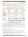
1
Freescale Semiconductor
Application Note
Document Number: AN4518
Rev. 1, 11/2015
Dual 3-Phase PMSM Development
Kit with MPC5643L
by:
Marek Stulrajter and Roman Filka
Contents
1 Introduction
1
Introduction................................................................1
This application note describes the design of a 3-phase
Permanent Magnet Synchronous Motor (PMSM) vector
control drive with 3-shunt current sensing with a position
sensor. It describes a modular concept that allows single and
dual PMSM configuration.
2
System Concept............................. ............................2
3
PMSM Field-Oriented Control.......... ....................... 2
4
MPC5643L - CB configuration.................................7
5
Software Design...................................................... 16
The design exhibits the suitability and advantages of the
MPC5643L microcontroller for single/dual motor control. It
serves as an example of a PMSM control design using a
Freescale 32-bit Qorivva microcontrollers built on the Power
ArchitectureTM technology optimized for a full range of
automotive applications.
6
Application Control User Interface..... ....................26
7
References.............................. ................................. 29
8
Revision history.......................... ............................ 29
The system is designed to drive one or two 3-phase PMSMs.
System features include:
• Modular s/w concept of 3-phase PMSM speed fieldoriented control that can be configured for single or dual
PMSM application
• Current sensing with three shunt resistors
• Support for encoder and resolver position transducers
• Application control user interface using FreeMASTER
debugging tool
• Motor Control Application Tuning (MCAT) tool
© 2015 Freescale Semiconductor, Inc.
System Concept
2 System Concept
The system is designed to drive either one 3-phase PMSM or two 3-phase PMSMs independently. The application meets the
following performance specifications:
• Targeted at the MPC5643L Controller; see the dedicated user manual for MPC5643L (see References)
• Running on the MPC5643L Control Drive board; see the dedicated user manual for MPC5643L Controller Board (see
References)
• Control technique incorporating:
• Vector control of 3-phase PMSM with position sensor
• Closed-loop speed control
• Bidirectional rotation
• Both motor and generator modes
• Closed-loop current control
• Flux and torque independent control
• Starting up with alignment
• Field weakening is not implemented in this SW version
• Reconstruction of 3-phase motor currents from two shunt resistors
• 100 µs sampling period with FreeMASTER recorder
• FreeMASTER software control interface (motor start/stop, speed setup) (see References)
• The control page offers a possibility to control two PMSMs independently
• Motor Control Application Tuning (MCAT) tool (see References)
• The MCAT tool is a user-friendly graphical FreeMASTER plug-in tool for debugging and tuning of motor-control
applications
• FreeMASTER software monitor
• FreeMASTER software graphical control page (required speed, actual motor speed, start/stop status, DC-Bus
voltage level, system status). FreeMASTER software speed scope (observes actual and desired speeds and DCBus voltage)
• FreeMASTER software high-speed recorders (reconstructed motor currents, vector control algorithm quantities)
• DC-Bus over-voltage and under-voltage, over-current, overload, and start-up fail protection
3 PMSM Field-Oriented Control
For dual PMSM configuration, the same field-oriented control (FOC) approach is used for both PMSMs.
3.1 Fundamental principle of PMSM FOC
High-performance motor control is characterized by smooth rotation over the entire speed range of the motor, full torque
control at zero speed, and fast acceleration/deceleration. To achieve such control, vector control techniques are used for
PMSMs. The vector control techniques are usually also referred to as field-oriented control.
The FOC concept is based on an efficient torque control requirement, which is essential for achieving high control dynamics.
Analogous to standard DC machines, AC machines develop maximal torque when the armature current vector is
perpendicular to the flux linkage vector. Therefore, if only the fundamental harmonic of stator-mmf is considered, the torque
Te developed by an AC machine, in vector notation, is given by:
Dual 3-Phase PMSM Development Kit with MPC5643L, Rev. 1, 11/2015
2
Freescale Semiconductor, Inc.
PMSM Field-Oriented Control
Equation 1.
where pp is the number of motor pole-pairs, is is the stator current vector and Ψs represents the vector of the stator flux.
Constant 3/2 indicates a non-power invariant form of transformation used.
In the case of DC machines, the requirement of having the rotor flux vector perpendicular to the stator current vector is
satisfied by the mechanical commutator. Because there is no such mechanical commutator in AC machines, the functionality
of the commutator has to be substituted electrically, by enhanced current control. This therefore implies orientation of the
stator current vector in such a way so as to isolate the component of stator current magnetizing the machine (flux component)
from the torque producing component. This can be accomplished by decomposing the current vector into two components
projected in the reference frame, often called the dq frame, that rotates synchronously with the rotor. It has become standard
to position the dq reference frame to have the d-axis aligned with the position of the rotor flux vector, so that current in the daxis will alter the amplitude of the rotor flux linkage vector. That requires the reference frame position to be updated such
that the d-axis will be always aligned with the rotor flux axis. Because the rotor flux axis is locked to the rotor position, for
PMSM machines, a mechanical position transducer can be used to measure the rotor position and hence position of the rotor
flux axis. Having the reference frame phase set so that the d-axis is aligned with the rotor flux axis, the current in the q-axis
represents solely the torque producing current component. Setting the reference frame speed to be synchronous with the rotor
flux axis speed results in both d and q axis current components having DC values. This implies utilization of simple current
controllers to control the demanded torque and magnetizing flux of the machine, simplifying the control structure design.
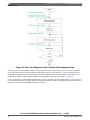
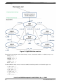
Figure 1 shows the basic structure of the vector control algorithm for the PMSM. To perform vector control, perform these
steps:
• Measure and obtain the motor states, variables and quantities. For example: phase voltages, currents, rotor speed, and
position.
• Transform quantities into the two-phase system (αβ) using a Clarke transformation.
• Transform stator currents into the dq reference frame using a Park transformation.
Also keep in mind:
• The stator current torque (isq) and flux (isd) producing components are separately controlled.
• The output stator voltage space vector is calculated using the decoupling block.
• The stator voltage space vector is transformed by an inverse Park transformation back from the d, q reference frame
into the two-phase system fixed with the stator.
• The output 3-phase voltage is generated using a space vector modulation.
To be able to decompose currents into torque and flux producing components (isq , isd), position of the motor-magnetizing
flux has to be known. This requires accurate sensing of the rotor position and velocity. Incremental encoders or resolvers
attached to the rotor are naturally used as position transducers for vector control drives.
Figure 1. Field-oriented control transformations
Dual 3-Phase PMSM Development Kit with MPC5643L, Rev. 1, 11/2015
Freescale Semiconductor, Inc.
3
PMSM Field-Oriented Control
3.2 PMSM model in quadrature phase synchronous reference
frame
Quadrature phase model in synchronous reference frame is very popular for FOC structures because both controllable
quantities, current and voltage, are DC values. This allows the use of only simple controllers to force the machine currents
into the defined states. Furthermore, full decoupling of the machine flux and torque can be achieved, which allows dynamic
torque, speed, and position control.
The equations describing voltages in the 3-phase windings of a permanent magnet synchronous machine can be written in
matrix form as follows:
Equation 2.
where the total linkage flux in each phase is given as:
Equation 3.
where:
•
•
•
•
Laa, Lbb, and Lcc are stator phase self inductances
Lab = Lba, Lbc = Lcb, and Lca = Lac are mutual inductance between respective stator phases
the term ΨPM represents the magnetic flux generated by the rotor permanent magnets
θe is the electrical rotor angle
Figure 2. Orientation of stator (stationary) and rotor (rotational) reference frames, with
current components transformed into both frames
Dual 3-Phase PMSM Development Kit with MPC5643L, Rev. 1, 11/2015
4
Freescale Semiconductor, Inc.
PMSM Field-Oriented Control
The voltage equation of the quadrature phase synchronous reference frame model can be obtained by transforming the 3phase voltage equations (Equation 1 on page 2, Equation 2 on page 4) into a 2-phase rotational frame which is aligned and
rotates synchronously with the rotor as shown in Figure 2. Such transformation, after some mathematical corrections, yields
the following set of equations:
Equation 4.
Equation 4 on page 5 represents a non-linear cross dependent system, with cross-coupling terms in both d and q axis and
back-EMF voltage component in the q-axis. When FOC is employed, both cross-coupling terms shall be compensated to
allow independent control of current d and q components. Design of the controllers is then governed by following pair of
equations, derived from Equation 4 on page 5 after compensation:
Equation 5.
Equation 6.
which describes the model of the plant for d and q current loop. Both equations are structurally identical, therefore the same
approach of controller design can be adopted for both d and q controllers. The only difference is in values of d and q axis
inductances, which results in different gains of the controllers. Considering closed loop feedback control of a plant model as
in either equation, using standard PI controllers, then the controller proportional and integral gains can be derived, using a
pole-placement method, as follows:
Equation 7.
Equation 8.
where ω0 represents Natural Frequency [rad s-1] and ζ is the Damping Factor [-] of the current control loop.
3.3 Phase current measurement
Figure 3 shows how the 3-phase voltage source inverter uses three shunt resistors (R32, R31, and R32) placed in each of the
inverter leg as phase current sensors. Stator phase current flows through the shunt resistor, producing a voltage drop which is
interfaced to the AD converter of the microcontroller through conditional circuitry. See “3-Phase BLDC/PMSM Low Voltage
Power Stage - User Manual” for more information.
Dual 3-Phase PMSM Development Kit with MPC5643L, Rev. 1, 11/2015
Freescale Semiconductor, Inc.
5
PMSM Field-Oriented Control
Figure 3. 3-phase DC/AC inverter with shunt resistors for current measurement
Figure 4 shows an operational amplifier and input signal filtering circuit which provides the conditional circuitry and adjusts
voltages to fit into the ADC input voltage range.
Figure 4. Phase current measurement conditional circuitry
The phase current sampling technique is a critical issue for detection of phase current differences and for acquiring full 3phase information of stator current by its reconstruction. Phase current flowing through shunt resistors produces a voltage
drop which needs to be appropriately sampled by the AD converter when low-side transistors are switched on. The current
cannot be measured by the current shunt resistors at an arbitrary moment. This is because the current flows through the shunt
resistor only when the bottom transistor of the respective inverter leg is switched on. Therefore, considering the diagram
depicted in Figure 3, phase A current is measured using the R30 shunt resistor and can be sampled only when the transistor
Q5 is switched on. Correspondingly, the current in phase B can be measured only if the transistor Q6 is switched on, and the
current in phase C can be measured only if the transistor Q7 is switched on. To get an actual instant of current sensing,
voltage waveform analysis has to be performed.
Generated duty cycles phase A, phase B, and phase C of two different PWM periods are depicted in Figure 5. These phase
voltage waveforms correspond to a center-aligned PWM with sinewave modulation. As shown in Figure 5 PWM period I, the
best sampling instant of phase current is in the middle of the PWM period, where all bottom transistors are switched on.
Dual 3-Phase PMSM Development Kit with MPC5643L, Rev. 1, 11/2015
6
Freescale Semiconductor, Inc.
MPC5643L - CB configuration
However, not all three currents can be measured at an arbitrary voltage shape. PWM period II in Figure 5 shows a case when
the bottom transistor of phase A is on for a very short time. If the on time is shorter than a certain critical time, dependent on
the h/w design, the current cannot be correctly measured.
Figure 5. Generated phase duty cycles in different PWM periods
In standard motor operation, where the supplied voltage is generated using the space vector modulation, the sampling instant
of phase current takes place in the middle of the PWM period in which all bottom transistors are switched on. If the
modulation index of applied SVM technique increases, there is an instant when one of the bottom transistors is switched on
for a very short time period. Therefore, only two currents are measured and the third one is calculated from equation:
Equation 9.
Therefore, a minimum on time of the low-side switch is required for 3-phase current reconstruction.
4 MPC5643L - CB configuration
The PMSM speed FOC framework application s/w and h/w configured for single or dual PMSM application is designed to
meet the following hardware configuration and technical specifications:
• MPC5643L Controller Board is used. See the dedicated user manual for MPC5643L Controller Board for more
information (see References).
• Two 3-phase low voltage power stages with MC33937 pre-driver are used
• See the dedicated user manual for 3-phase low voltage power-stage with MC33937 pre-driver (see References).
• See the dedicated user manual for MC33937 pre-driver (see References).
• See the dedicated document describing communication with and configuration of MC33937 pre-driver using
DSPI communication bus
NOTE
For single motor application, only one low voltage power stage is necessary.
•
•
•
•
PWM output frequency of both PWM modules = 20kHz
Current loop sampling period = 100 s
Speed loop sampling period = 1ms
3-phase current measurement using three shunt resistors on bottom side of each inverter leg. Phase current
measurement feedback of both motors is routed to ADC0 and ADC1 as follows:
• M1_UNI3 - phase A current: ADC0/1 - CH11
• M1_UNI3 - phase B current: ADC0/1 - CH12
Dual 3-Phase PMSM Development Kit with MPC5643L, Rev. 1, 11/2015
Freescale Semiconductor, Inc.
7
MPC5643L - CB configuration
•
•
•
•
M1_UNI3 - phase C current: ADC0 - CH2
M2_UNI3 - phase A current: ADC0/1 - CH13
M2_UNI3 - phase B current: ADC0/1 - CH14
M2_UNI3 - phase C current: ADC1 - CH2
NOTE
For single motor application only one of the UNI3 connectors is selected.
• DC bus voltage measurement for both power stages routed to ADC0 as follows:
• M1_UNI3 - DC bus voltage: ADC0 - CH1
• M2_UNI3 - DC bus voltage: ADC0 - CH3
NOTE
For single motor application the same UNI3 connector as for current sensing is
selected.
• Encoder position feedback routed to eTimer0 and eTimer1 modules as follows:
• Primary encoder phase A, (JP500): eTimer0 - CH0, Counter #0 input
• Primary encoder phase B, (JP500): eTimer0 - CH0, Counter #1 input
• Secondary encoder phase A, (JP501): eTimer1 - CH0, Counter #1 input
• Secondary encoder phase B, (JP501): eTimer1 - CH0, Counter #2 input
NOTE
For single motor application only one of the Encoders is selected.
• Resolver excitation signal routed from
• Primary resolver excitation, (J200): eTimer1 - CH5
• Secondary resolver excitation, (J250): eTimer1 - CH4
NOTE
For single motor application, only one of the eTimer’s channels is selected,
according to the selected resolver.
• Resolver position feedback signals for both motors routed to ADC0 and ADC1 as follows:
• Primary resolver sin, (J200): ADC0 - CH0
• Primary resolver cos, (J200): ADC1 - CH0
• Secondary resolver sin, (J250): ADC0 - CH6
• Secondary resolver cos, (J250): ADC1 - CH6
NOTE
For single motor application, only one of the Resolvers is selected.
4.1 FlexPWM
The MPC5643L Clock Generation Module is configured to generate a clock signal of 120MHz on the MC_PLL_CLK bus.
The Pulse Width Modulator module (FlexPWM) is clocked from the MC_PLL_CLK, therefore it is placed behind the IPS
Bus Clock Sync Bridge.
The MPC5643L device contains four PWM channels, each of which is configured to control a single half-bridge power stage.
Two modules are included on 257 MAPBGA devices; on the 144 LQFP package, only one module is present. Targeted
MPC5643L Control Drive board is based on 257 MAPBGA device and therefore each of the FlexPWM modules is used to
control 3-phase PMSM. FlexPWM_0 is dedicated for Motor #1 and FlexPWM_1 is dedicated for Motor #2. Both FlexPWM
modules are synchronized using the Master Reload Signal (MRS), as shown in Figure 7.
Dual 3-Phase PMSM Development Kit with MPC5643L, Rev. 1, 11/2015
8
Freescale Semiconductor, Inc.
MPC5643L - CB configuration
The FlexPWM_0 submodule #0 is configured to run as a master and to generate MRS and counter synchronization signal
(master sync) for other submodules in FlexPWM module 0 and module 1. The MRS signal is generated every second
opportunity of submodule #0, VAL1 compare, that is, full cycle reload. All double buffered registers, including compare
registers VAL2, VAL3, VAL4, and VAL5 are updated on the occurrence of MRS, therefore new PWM duty cycles iare
updated every two PWM periods.
FlexPWM modulo counting, for generation of center-aligned PWM signals, is achieved by setting VAL0 register to zero and
INIT register to negative value of VAL1. When PWM clock of 120MHz, required PWM output 20kHz, and PWM reload
period 100 µs, then INIT, VAL,0 and VAL1 registers of submodules 0, 1, and 2 are set as follows:
• INIT = -120000000/20000/2 = -3000 DEC = 0xF448
• VAL0 = 0 DEC
• VAL1 = - INIT - 1 = 2999 DEC = 0x0BB7
Reload frequency of FlexPWM_0 submodules 0, 1, and 2 is set to “Every two opportunities“ and “Full cycle reload” is
enabled. Because submodule #0 is a master that generates MRS signal, reload of double buffered registers of submodule #0 is
done on Local Reload. Submodules 1 and 2 are slaves, therefore reload of their double buffered registers is done on Master
Reload, broadcast from submodule #0. Similarly, submodules #0 counter is initialized on Local Sync event, while
submodules 1 and 2 on Master Sync event again are broadcast from submodule #0.
Because some registers are double buffered on occurrence of FORCE OUT signal, all submodules of FlexPWM_0 have as
force source selected Local Reload event.
There are several ways to set FlexPWM_1. In this application, synchronized outputs of both FlexPWM_0 and FlexPWM_1
with no phase shift are required. The MRS signal is used as a source of external synchronization signal EXT_SYNC to
initialize the PWM counter of FlexPWM_1. Reload frequency of submodules 0, 1, and 2 is set to “Every
opportunity“ because the MRS signal is already generated at every second opportunity in FlexPWM_0. “Full cycle reload” is
enabled in all submodules of FlexPWM_1. Reload of double-buffered registers of submodule #0 is done on Local Reload.
Submodules 1 and 2 are slaves, therefore reload of their double buffered registers is done on Master Reload, broadcast from
submodule #0. Counters of submodules 0, 1, and 2 are initialized on Ext Sync event.
Some registers are double buffered at the occurrence of FORCE OUT signal. In FlexPWM_1, the selected force source is:
• Submodule 0: Local Sync event
• Submodules 1 and 2: Master Sync event
All PWM channels are used to drive a 3-phase DC/AC inverter, therefore each PWM pair is driven in complementary mode,
with dead-time automatically added on each rising edge of the respective PWM signal. Used power stage with MC33937 predriver inverts the polarity of PWM signals for top transistors (active low logic) so PWM A output polarity in all submodules
is set as Inverted. Therefore, the output of PWM A of each submodule is set to logic one during the fault state as well.
FlexPWM modules include a Fault Protection logic, which can control any combination of PWM output pins and
automatically disable PWM outputs during a fault state. Faults are generated by a logic one on any of the FAULTx pins. To
enable mapping of all fault pins, fault disable mapping registers (DISMAP) of all submodules must be enabled (logic one).
4.2 CTU
The MRS signal generated from the FlexPWM module is internally routed to the Cross Triggering Unit (CTU) module,
where it is selected using the input selection register Trigger Generator Subunit Input Selection Register (TGSISR) as the
source of master reload signal for CTU. This signal is used to reload trigger compare registers and to reload the TGS counter
with the value stored in the TGS counter reload register. The TGS counter register is used to compare the current counter
value with the values of trigger compare registers. When the two values are the same, an event is generated. TGS is
configured in triggered mode.
Because the MRS signal is generated every two PWM periods, the CTU counter can count up to value of 12000DEC
considering the initial value is set to zero.
Following TGS trigger compare registers are used for trigger events:
Dual 3-Phase PMSM Development Kit with MPC5643L, Rev. 1, 11/2015
Freescale Semiconductor, Inc.
9
MPC5643L - CB configuration
• T0CR = 0x0 (0 DEC)
• T1CR = 0x0A82 (2690 DEC)
• 1 T2CR = 0x21F2 (8690 DEC)
• T3CR = 0x2DF0 (11760 DEC)
Trigger events T1CR and T2CR must reflect the phase shift between square and filtered excitation signal. If a 3-order filter is
used, then a new setting of the compare registers is required:
• T1CR = 0x28FA (10490 DEC)
• 2 T2CR = 0x118A (4490 DEC)
The CTU Scheduler subUnit (SU) generates the trigger event output according to the occurred trigger event. The following
trigger event outputs are generated:
• ADC command output: T0CR generates ADC command event output, with command offset initially set to one. It is
used as the synchronization signal to ADC (ADC commands #0 - #1 for phase current and DC bus voltage
measurement of motor connected to M1_UNI3 and ADC commands #2 - #3 for phase current and DC bus voltage
measurement of motor connected to M2_UNI3).
• eTimer1 output: T1CR generates eTimer1 event output, which toggles its output to generate rising edge of resolver
exciting signal. T1CR is phase shifted to account for the delay caused by the MPC5643L resolver h/w circuitry and to
allow ADC sampling of resolver signals just before PWM reload.
• eTimer1 output: T2CR generates eTimer1 event output, which toggles its output to the generate falling edge of the
resolver exciting signal; frequency of resolver exciting signal is: resolverSignalFreq = MC_PLL_CLK/(2*(T2CRT1CR)) = 120000000/(2*(8460-2460))=10kHz.
• ADC command output: T3CR generates ADC command event output, with command offset set to zero. It is used as the
synchronization signal to ADC (ADC command #22 for primary resolver signals and ADC command #23 for
secondary resolver signals sampling).
NOTE
Trigger event outputs T1CR, T2CR, and T3CR are necessary only when using the
resolver position sensor.
The SU uses a Commands List in order to select the command to send to the ADC when a trigger event occurs. Each ADC
command sent by the CTU into the ADC specifies:
•
•
•
•
Whether the actual command is the first command of a new stream of consecutive commands or not
Whether an End Of Conversion (EOC) interrupt is issued when conversion specified by the command is finished
Which channels are to be converted for both ADC modules
The target FIFO register for storing the conversion results
Because the trigger compare register for trigger T0CR is set to zero, it generates the ADC start of conversion request at the
beginning of each PWM reload cycle. When a T0CR trigger event occurs, the ADC command selected by the index value
T0_INDEX in command list control registers CLCR1 is sent to the ADC. At each T0CR trigger event, two ADC commands
are executed in a stream. The first command in a stream specifies two phase currents to be sampled simultaneously (all phase
current signals are routed to pins shared between both ADC modules), and the second command specifies the third phase
current and DC bus voltage to be sampled.
The index pointer to the ADC command list T0_INDEX is updated according to the sector in which the actual output voltage
vector resides, calculated by the space vector modulation of the FOC algorithm. There are six sectors within the output
voltage hexagon of the inverter, therefore six different ADC command sequences are selected for one full revolution of the
voltage vector. This technique is necessary when the phase current measurement is done using three shunt resistors placed in
the bottom side of each inverter leg. Because the shunt resistor is placed at the bottom side of the inverter leg, the phase
current can be measured only when bottom transistor is switched on. Because the sum of the three currents in the motor
windings is zero, only two currents are measured and the third is calculated. Which phases are measured and which are
calculated changes according to the voltage vector angle, that is, the phases with the largest PWM on-pulse on the bottom
transistors are selected to get the best current information.
1.
2.
These values are used when square and filtered excitation signals are in phase, as shown in Figure 9.
These values are used when square and filtered excitation signals are phase shifted due to an analog filter.
Dual 3-Phase PMSM Development Kit with MPC5643L, Rev. 1, 11/2015
10
Freescale Semiconductor, Inc.
MPC5643L - CB configuration
Configuration of CTU ADC commands is shown in Figure 6.
Figure 6. Configuration of CTU ADC commands for the PMSM FOC application
4.3 eTimer0
This eTimer module is only used for decoding two square-wave signals from a primary encoder, such as the JP500 connector.
4.3.1 Primary encoder
Because of h/w design, a channel #0 of this eTimer module is selected. The purpose is to decode the two ninety degrees
shifted square-wave signals and count up or down all rising/falling edges based on their sequence. Software routine then
reads the associated counter value to get the information about rotor position. Reading of the counter value is performed from
within POSPE_GetPositionElEnc() function, periodically within CTU-ADC interrupt service routine; see the data flow
diagram shown in Figure 11. Parameters entering POSPE_GetPositionElEnc() represent a PMSM drive structure related
to Motor #1.
In order to decode the encoder signals, the timer channel #0 of module eTimer0 (eTimer0-ETC[0]) is configured as follows:
•
•
•
•
•
•
Counting mode - Quadrature count mode, uses primary and secondary sources
Count direction - Count Up
Primary source - Counter #0 input
Secondary source - Counter #1 input
Count stop mode - Count Repeatedly
Count length - Count Until Compare then Reinitialize
Dual 3-Phase PMSM Development Kit with MPC5643L, Rev. 1, 11/2015
Freescale Semiconductor, Inc.
11
MPC5643L - CB configuration
• Preload control for CNTR
• Load CNTR with CMPLD1 upon successful compare with COMP2
• Load CNTR with CMPLD2 upon successful compare with COMP1
• Compare mode - Use COMP1 when counting up and COMP2 when counting down
• Output mode - Toggle OFLAG on successful compare with COMP1 and/or COMP2
• COMP1 = 0x07FF (2047 DEC)
• COMP2 = 0xF800 (-2048 DEC)
• CMPLD1 = 0x07FF (2047 DEC)
• CMPLD2 = 0xF800 (-2048 DEC)
• LOAD = 0x0, this value is updated by a software routine during ALIGN phase
The compare registers of eTimer0 channel #0 are set according to the number of encoder pulses per one mechanical
revolution. In this case, an encoder sensor with 1024 pulses is used. In quadrature mode, it means the encoder capability of
position recognition with a precision that is four times higher than the number of pulses in the application, the maximum
numbers of edges is 4096. Then the compare registers are calculated as follows:
• COMP1 = 4096/2 - 1 = 2047 (0x07FF HEX)
• COMP2 = -4096/2 = -2048 (0xF800 HEX)
4.4 eTimer1
This eTimer module is used for encoder signal decoding as well as for resolver excitation signals generation.
4.4.1 Secondary encoder
Because of h/w design, a channel #0 of this eTimer module is selected for decoding two square-wave signals from a
secondary encoder (JP501 connector). The purpose is described in Primary encoder. Reading of the counter value is
performed from within the POSPE_GetPositionElEnc() function, periodically within CTU-ADC interrupt service routine;
see the data flow diagram shown in Figure 10. Parameters entering POSPE_GetPositionElEnc() represent a PMSM drive
structure related to Motor #2.
To decode the encoder signals, timer channel #0 of module eTimer1 (eTimer1-ETC[0]) is configured as follows:
•
•
•
•
•
•
•
•
•
•
•
•
•
•
Counting mode - Quadrature count mode, uses primary and secondary sources
Count direction - Count Up
Primary source - Counter #1 input
Secondary source - Counter #2 input
Count stop mode - Count Repeatedly
Count length - Count Until Compare then Reinitialize
Preload control for CNTR
• Load CNTR with CMPLD1 upon successful compare with COMP2
• Load CNTR with CMPLD2 upon successful compare with COMP1
Compare mode - Use COMP1 when counting up and COMP2 when counting down
Output mode - Toggle OFLAG on successful compare with COMP1 and/or COMP2
COMP1 = 0x07FF (2047 DEC)
COMP2 = 0xF800 (-2048 DEC)
CMPLD1 = 0x07FF (2047 DEC)
CMPLD2 = 0xF800 (-2048 DEC)
LOAD = 0x0, this value is updated by a software routine during ALIGN phase
The compare registers of eTimer1 channel #0 are set according to the number of encoder pulses per one mechanical
revolution. In this case, an encoder sensor with 1024 pulses is used. For compare registers settings, see Primary encoder.
Dual 3-Phase PMSM Development Kit with MPC5643L, Rev. 1, 11/2015
12
Freescale Semiconductor, Inc.
MPC5643L - CB configuration
4.4.2 Primary resolver
The eTimer1 module can be further used for generation of an exciting signal for primary resolver (J200 connector). Because
of h/w design, channel #5 of this eTimer module is selected. The purpose is to generate a square wave signal with frequency
10kHz which is then processed by a hardware low pass filter designed on used controller board. Because of the low pass
filter, the resulting harmonic signal is phase shifted.
To generate such a square wave signal, synchronized with the MRS signal, timer channel #5 of module eTimer1 (eTimer1ETC[5]) is configured as follows:
•
•
•
•
•
•
•
•
•
•
•
•
•
Counting mode - Edge of secondary source triggers primary count till compare
Count direction - Count Up
Primary source - IPBus clock
Secondary source - AUX #0, which is an output signal from CTU ETIMER #1 trigger event output
Polarity of secondary source - True/Inverted
Count stop mode - Count Repeatedly
Count length - Count Until Compare then Reinitialize
Compare mode - Use COMP1 when counting up and COMP2 when counting up
Output mode - Toggle OFLAG on successful compare with COMP1 and/or COMP2
COMP1 = 0x0
COMP2 = 0x0
LOAD = 0x0
Direction of the channel pin - Output - OFLAG
4.4.3 Secondary resolver
The eTimer1 module can be further used for generation of an exciting signal for secondary resolver (J250 connector).
Because of h/w design, channel #4 of this eTimer module is selected. The purpose is to generate a square wave signal with
frequency 10kHz which is then processed by a hardware low pass filter designed on used controller board. Because of the
low pass filter, the resulting harmonic signal is phase shifted.
To generate such a square wave signal, synchronized with the MRS signal, timer channel #4 of module eTimer1 (eTimer1ETC[4]) is configured as follows:
•
•
•
•
•
•
•
•
•
•
•
•
•
Counting mode - Edge of secondary source triggers primary count till compare
Count direction - Count Up
Primary source - IPBus clock
Secondary source - AUX #0, which is an output signal from CTU ETIMER #1 trigger event output
Polarity of secondary source - True/ Inverted3
Count stop mode - Count Repeatedly
Count length - Count Until Compare then Reinitialize
Compare mode - Use COMP1 when counting up and COMP2 when counting up
Output mode - Toggle OFLAG on successful compare with COMP1 and/or COMP2
COMP1 = 0x0
COMP2 = 0x0
LOAD = 0x0
Direction of the channel pin - Output - OFLAG
3.
True is selected when square and filtered excitation signals are in phase, as shown in Figure 9. Inverted is selected
when square and filtered excitation signals are phase shifted due to an analog filter.
Dual 3-Phase PMSM Development Kit with MPC5643L, Rev. 1, 11/2015
Freescale Semiconductor, Inc.
13
MPC5643L - CB configuration
4.5 On-chip motor control peripherals interconnection
Figure 7 shows how the CTU interacts with the following peripherals:
•
•
•
•
•
ADC0 and ADC1
DSPI1
eTimer0, eTimer1, and eTimer2
FlexPWM_0 and FlexPWM_1
FlexRay
Figure 7. MPC5643L motor control peripherals connection
4.6 ADC conversion and interrupt timing
Configuration of FlexPWM, CTU, eTimer0, and eTimer1 peripheral modules, as described in FlexPWM, CTU, eTimer0, and
eTimer1, results in a sequence of triggers/events that are shown in Figure 8. The application state machine functions are
called from an interrupt service routine, which is associated with CTU-ADC command interrupt request. As shown in the
ADC command list configuration of Figure 6, the ADC command interrupts are linked with CTU trigger T0CR, that is, when
measurement of the phase currents and DC bus voltage is finished.
Dual 3-Phase PMSM Development Kit with MPC5643L, Rev. 1, 11/2015
14
Freescale Semiconductor, Inc.
MPC5643L - CB configuration
Figure 8. FlexPWM-CTU-ADC conversion timing
For correct calculation of the FOC algorithm, resolver, and phase current measurements must be executed at the same time.
Because there are only two independent sample and hold circuitries on MPC5643L, parallel sampling of all signals is
impossible. Two phase currents can be read at the same time and two resolver signals can be read at the same time. The two
measurements of these four signals must, however, be sequenced one after another. The sequence of these two measurements
is handled by CTU triggers T0CR and T3CR.
Because ADC channels of resolver signals do not have to be changed according to the generated voltage vector, as in case of
phase currents, there is only one CTU-ADC command for one particular resolver assigned to initiate sampling of resolver
signals:
• ADC command #22 for the primary resolver
• ADC command #23 for the secondary resolver
This sampling/conversion is triggered by the CTU trigger T3CR, which is delayed in time to sample both resolver signals at
the point of their maximal amplitude variation, see Figure 9.
CTU triggers T1CR and T2CR generate the resolver exciting signal phase shifted to fulfill the following requirements:
• The point where amplitude of both resulting resolver signals varies the most must be as close as possible before phase
currents measurement to ensure position and current samples correspond to each other.
• Keep 50% duty-cycle ratio of the resolver exciting signal.
Dual 3-Phase PMSM Development Kit with MPC5643L, Rev. 1, 11/2015
Freescale Semiconductor, Inc.
15
Software Design
Figure 9. An envelope extractor of resolver feedback signals
5 Software Design
5.1 Introduction
This section describes the software design of the PMSM FOC framework application that can be used for the configuration of
either one or two synchronous motors. The application overview and description of software implementation are provided.
The aim of this chapter is to help in understanding of the designed software.
5.2 Application software design
To make the software easily applicable for one or multi-motor application, all parameters and variables are grouped in a
specific data structure. In this application, data structure pmsmDrive_t represents a predefined format that is used for
organizing and storing data for the purpose of working on it with various algorithms, routines, and functions.
The following is the general structure for PMSM:
typedef struct{
AppFaultStatus
AppFaultStatus
tU32
SWLIBS_2Syst
SWLIBS_2Syst
SWLIBS_2Syst
SWLIBS_2Syst
SWLIBS_2Syst
SWLIBS_2Syst
SWLIBS_2Syst
SWLIBS_2Syst
SWLIBS_2Syst
faultID;
faultIDp;
svmSector;
iDQFbck;
iAlBeFbck;
iDQReq;
uDQReq;
iDQReqZC;
iDQErr;
uAlBeReq;
uAlBeReqDCB;
thTransform;
//
//
//
//
//
//
//
//
//
//
//
//
Application faults
Application faults flags
Space Vector Modulation sector
dq axis current feedback
Alpha/Beta - axis current feedback
dq axis required currents, given by speed PI
dq axis required voltages given by current PIs
Zero cancellation in current branch
Error between the reference and feedback signal
Alpha/Beta required voltages
Al/Be voltages after DC Bus ripple elimination
Transformation angle - enters Park transform.
Dual 3-Phase PMSM Development Kit with MPC5643L, Rev. 1, 11/2015
16
Freescale Semiconductor, Inc.
Software Design
SWLIBS_3Syst
iAbcFbck;
// 3-phases current feedback
SWLIBS_3Syst
pwm32;
// 3-phase 32bit Duty-Cycles from uAlBeReqDCB
FLEXPWM_VAL_COMPL
pwm16;
// 3-phase 16bit Duty-Cycles feeding PWM registers
GMCLIB_ELIMDCBUSRIP_T
elimDcbRip;
// DC Bus voltage ripple elimination
GFLIB_CONTROLLER_PIAW_R_T
dAxisPI;
// d-axis current PI controller
GFLIB_CONTROLLER_PIAW_R_T
qAxisPI;
// q-axis current PI controller
GFLIB_CONTROLLER_PIAW_P_T
speedPI;
// Speed PI controller
GFLIB_RAMP_T
speedRamp;
// Reference speed ramp generation
GDFLIB_FILTER_IIR1_T dAxisZC;
// d-axis current zero cancellation
GDFLIB_FILTER_IIR1_T qAxisZC;
// q-axis current zero cancellation
GDFLIB_FILTER_IIR1_T uDcbFilter;
// DC bus voltage filter settings
adcModulePmsm_t
adc;
// ADC measurement
pospeModule_t
pospeRes;
// Position/Speed module for resolver
pospeModule_t
pospeEnc;
// Position/Speed module for encoder
pospeControl_t
pospeControl;
// Position/Speed variables needed for control
uni3PeriphCfgPmsm_t
uni3PeriphCfg; // ADC measurement channels configuration
pospePeriphCfg_t
pospeCfg;
// Encoder/Resolver configuration
MC33937_SET_T
preDrv;
// PreDriver configuration
driveStates_t
cntrState;
// State machine parameters, switches states
scalarControl_t
scalarControl; // Scalar Control states variables
}pmsmDrive_t;
The proposed structure includes all variables related to cascade structure for PMSM FOC, state variables related to the
application, and data for peripherals configuration such as base address or channel offset.
The declaration of structures used for different motors can be as follows:
pmsmDrive_t
pmsmDrive_t
pmsmDrive_t
M1;
M2;
Mx;
//related to Motor #1
//related to Motor #2
//related to Motor #x
The names of all variables are composed of a prefix given by the name of structure Mx and the name of the variables/
structures which are members of the main structure pmsmDrive_t. For instance: M1.iAbcFbck.s32Arg1 represents phase
A current of the Motor #1 or M2.iDQReq.s32Arg2 represents q-axis current of the Motor #2. The list of cascade structure
variables can be seen on Figure 13, where the block scheme of FOC for Motor #1 is shown and all FOC variables are
described.
5.3 Application data flow overview
The application software is interrupt driven running in real time. There is one periodic interrupt service routine associated
with CTU-ADC command interrupt request, executing all motor control tasks. These include both fast current and slow speed
loop control. All tasks are performed in an order described by the application state machine shown on Figure 12 and
application flowcharts shown on Figure 10 and Figure 11.
Dual 3-Phase PMSM Development Kit with MPC5643L, Rev. 1, 11/2015
Freescale Semiconductor, Inc.
17
Software Design
Figure 10. Flow chart diagram of main function with background loop
To achieve precise and deterministic sampling of analog quantities and to execute all necessary motor control calculations,
the state machine functions are called within a periodic interrupt service routine. Therefore, to call state machine functions,
the periphery causing this periodic interrupt must be properly configured and the interrupt enabled. As described later, all
peripherals are initially configured and all interrupts are enabled before calling the state machine, see Figure 12.
As soon as interrupts are enabled and all peripheries are correctly configured as described in MPC5643L - CB configuration,
the state machine functions are called from the CTU-ADC interrupt service routine. The background loop handles noncritical
timing tasks, such as the FreeMASTER communication polling.
Dual 3-Phase PMSM Development Kit with MPC5643L, Rev. 1, 11/2015
18
Freescale Semiconductor, Inc.
Software Design
Figure 11. Flow chart diagram of periodic interrupt service routine
5.4 State machine
The application state machine is implemented using a two-dimensional array of pointers to functions variable called
state_table[][](), with the first parameter describing current application event and the second parameter describing
actual application state. These two parameters select a particular pointer to state machine function, which causes a function
call whenever state_table[][]() is called.
Dual 3-Phase PMSM Development Kit with MPC5643L, Rev. 1, 11/2015
Freescale Semiconductor, Inc.
19
Software Design
Figure 12. Application state machine
The application state machine consists of the following six states, selected using variable state defined as AppStates:
•
•
•
•
•
•
INIT - state = 0
FAULT - state = 1
READY - state = 2
CALIB - state = 3
ALIGN - state = 4
RUN - state = 5
To indicate/initiate a change of state, 12 events are defined, selected using variable event defined as AppEvents:
•
•
•
•
•
•
•
e_fault - event = 0
e_fault_clear - event = 1
e_init - event = 2
e_init_done - event = 3
e_ready - event = 4
e_app_on - event = 5
e_calib - event = 6
Dual 3-Phase PMSM Development Kit with MPC5643L, Rev. 1, 11/2015
20
Freescale Semiconductor, Inc.
Software Design
•
•
•
•
•
e_calib_done - event = 7
e_align - event = 8
e_align_done - event = 9
e_run - event = 10
e_app_off - event = 11
After power on or reset, all used peripherals are reset and configured as required by the application; see MPC5643L - CB
configuration. To configure the application peripheral modules correctly, the all of the interrupts are disabled at the beginning
of peripheral reset and configuration section. Therefore, the periodic CTU-ADC interrupt is not requested and the state
machine functions cannot be executed until all of the interrupts are enabled and all peripherals are set.
To initialize all application variables and parameters, a state INIT is called as a first state/function of state machine. To fulfill
this condition, the application state and event are set to event = e_init and state = init before entering background
loop.
All interrupts are enabled after successful peripherals configuration. From this point, the CTU-ADC interrupts are enabled.
Therefore considering correct configuration of the peripherals, the first call of the state machine function will be from within
the CTU-ADC interrupt service routine.
5.5 State - INIT
The state INIT is a first called state/function of the state machine and can be entered from all states except the READY state,
provided there are no faults detected. All application variables and parameters are initialized in the state INIT.
After successful initialization, the application event is automatically set to event=e_init_done at the end of execution of
the INIT state and the state READY is selected as the next state to enter.
According to the data flow diagram of the CTU-ADC interrupt service routine, shown on Figure 11, the routine for 3-phase
current reconstruction ADC_Measure2Ph() is executed first, followed by the DC bus voltage measurement and the rotor
position measurement routine. The fault detection function is called always before the state machine function call, ensuring
correct transition to the FAULT state in case there is a fault detected. If there is no fault detected, the application event
remains set to event=e_init_done, and the READY state will be selected as next state to execute.
5.6 State - FAULT
The application goes into this state immediately when a fault is detected. The system allows all states to pass into the FAULT
state by setting event = e_fault. The state FAULT is a state that allows transition back to itself if a fault is present in the
system and the user does not request clearing of fault flags.
There are two different variables to signalize fault occurrence in the application. The actual fault register faultID represents
the current state of the fault pin/variable, and so on, and the pending fault register faultIDp represents a fault flag, which is
set when the actual fault is/was true. Even if the actual fault is reset, that is, the fault source disappears, pending fault remains
set until manually cleared by the user. Such a mechanism allows for stopping the application and analyzing the cause of
failure even if the fault was caused by a short glitch on monitored pins/variables.
The state FAULT can be left only when application variable switchFaultClear is manually set to true using FreeMASTER.
That is, the user has acknowledged that the fault source has been removed and the application can be restarted. When the user
sets switchFaultClear = true; the following sequence is automatically executed:
faultID.R
faultIDp.R
switchFaultClear
event
=
=
=
=
0x0;
0x0;
false;
e_fault_clear;
//
//
//
//
Clear Fault register
Clear Pending Fault register
Reset fault clearing switch
new application event
Dual 3-Phase PMSM Development Kit with MPC5643L, Rev. 1, 11/2015
Freescale Semiconductor, Inc.
21
Software Design
Setting event to event = e_fault_clear while in the FAULT state represents a new request to proceed to the INIT state.
This request is purely user activated and does not depend on the actual fault status, that is, it is up to the user when he decides
to set switchFaultClear true. However, according to the interrupt data flow diagram shown in Figure 11, function
faultDetection() is called before state machine function state_table[event][state](). Therefore, all faults will
be checked again and if there is any fault condition remaining in the system, the respective bit in faultID and faultIDp
variables will be set. As a consequence of faultID and faultIDp not being equal to zero, function faultDetection()
will modify the application event from e_fault_clear back to e_fault, which means a jump to fall state when state
machine function state_table[event][state]() is called. Therefore, the INIT state will not be entered even though
user tried to clear the fault flags using switchFaultClear.
When the next state (INIT) is set entered all fault bits are cleared, that means no fault is detected (faultIDp.R = 0x0) and
application variable switchFaultClear is manually set to true.
5.6.1 Application faults
Both faultID and faultIDp are defined as AppFaultStatus, which is a 32bit long data type. Application faults are bit
mapped in AppFaultStatus type as follows:
Table 1. AppFaultStatus type
31
30
29
FLT
FLT
FLT
31
30
29
15
14
13
12
11
10
FLT
FLT
FLT
FLT
FLT
FLT
15
14
13
12
11
10
•
•
•
•
•
•
•
•
•
•
•
•
•
•
•
•
•
•
•
•
•
•
•
•
28
27
26
25
24
23
22
21
FLT
FLT
FLT
FLT
24
23
22
21
9
8
7
6
5
4
FLT9
FLT8
FLT7
FLT6
FLT5
FLT4
RESERVED
20
19
18
17
16
FLT
FLT
FLT
18
17
16
3
2
1
0
FLT3
FLT2
FLT1
FLT0
RESERVED
FLT0 - OverDCBusVoltage (Over-voltage on DC bus)
FLT1 - UnderDCBusVoltage (Under-voltage on DC bus)
FLT2 - OverDCBusCurrent (Over-current on DC bus)
FLT3 - OverLoad (Overload Flag)
FLT4 - MainsFault (Mains out of range)
FLT5 - WrongHardware (Wrong hardware fault flag)
FLT6 - OverHeating (Overheating fault flag)
FLT7 - OverPhaseACurrent (Over-current on phase A)
FLT8 - OverPhaseBCurrent (Over-current on phase B)
FLT9 - OverPhaseCCurrent (Over-current on phase C)
FLT10 - OffCancError (Offset cancellation error)
FLT11 - MC33937_TLIM (over temperature) - not used in current s/w version
FLT12 - MC33937_DESAT (desaturation detected) - not used in current s/w version
FLT13 - MC33937_VLS (low VLS detected) - not used in current s/w version
FLT14 - MC33937_OC (over current detected) - not used in current s/w version
FLT15 - MC33937_PhaseE (phase error) - not used in current s/w version
FLT16 - MC33937_FrameE (SPI communication frame error) - not used in current s/w version
FLT17 - MC33937_WriteE (SPI communication write error) - not used in current s/w version
FLT18 - MC33937_RST (reset event) - not used in current s/w version
FLT21 - FOCError (error in FOC calculation function)
FLT22 - AlignError (error during alignment)
FLT23 - CalibError (error during ADC calibration)
FLT24 - InitError (error during app initialization)
FLT29 - FLEXPWM_Error (error in FlexPWM hw initialization)
Dual 3-Phase PMSM Development Kit with MPC5643L, Rev. 1, 11/2015
22
Freescale Semiconductor, Inc.
Software Design
• FLT30 - ADC_Error (error in ADC hw initialization)
• FLT31 - CTU_Error (error in CTU hw initialization)
5.7 State - READY
The state READY is a state that allows transition back to itself, provided no faults are present and the user does not request
the start of the application (by switchAppOnOff=true). This is a wait state where the application waits for the user to initiate a
transition to a following state.
Transition to the FAULT state is performed automatically when a fault occurs.
Transition to the CALIB state is performed by setting event to event=e_app_on, which is done automatically on the rising
edge of switchAppOnOff=true using FreeMASTER.
5.8 State - CALIB
In this state, ADC DC offset calibration is performed. When the state machine enters the CALIB state, all PWM outputs are
enabled.
Calibration of the DC offset is achieved by generating 50% duty-cycle on the PWM outputs and taking several measurements
of all configured ADC channels. These measurements are then averaged and the average value for each channel is stored.
This value will be subtracted from the measured value when in normal operation. In this way, the half-range DC offset,
caused by voltage shift of 1.65V in conditional circuitry, as shown in Figure 4, is removed in all three phases.
The state CALIB is a state that allows transition back to itself, provided no faults are present, the user does not requested stop
of the application (by switchAppOnOff=true), and the calibration process has not finished.
The number of samples for averaging is set by default to 28=256 and can be modified in the state INIT.
When all 256 samples have been taken and the averaged values successfully saved, the application event is automatically set
to event=e_calib_done and state machine can proceed to the state ALIGN.
Transition to the FAULT state is performed automatically when a fault occurs.
Transition to the INIT state is performed by seting event to event=e_app_off, which is done automatically on falling edge
of switchAppOnOff=false using FreeMASTER.
5.9 State - ALIGN
Alignment of the rotor and stator flux vectors is used to mark zero position, necessary only for relative position sensors such
as encoders and so on. When using a relative position sensor such as encoder, the zero position is not known, therefore the
counting of encoder edges has to be correctly reset at the start of operation. This is done in the ALIGN state, where a DC
voltage is applied in phase A for a certain period. This will force the rotor to rotate to “align” position, that is, the stator and
rotor fluxes are aligned. The rotor position in which the rotor stabilizes after applying this DC voltage is set as zero position,
therefore the timers eTimer0-CH0 and/or eTimer1-CH0, depending on the configuration, are reset to zero.
To wait for the rotor to stabilize in an aligned position, a certain time period is selected during which the DC voltage is
constantly applied. This time and amplitude of the DC voltage can be modified in the INIT state. Timing is implemented
using a s/w counter that counts from a predefined value down to zero. During this time, the event remains set to
event=e_align. When the counter reaches zero, the counter is reset back to a predefined value, timers eTimer0-CH0 and/or
eTimer1-CH0, depending on the configuration, are reset, and the event is automatically set to event=e_align_done. This
enables transition to the RUN state.
Transition to the FAULT state is performed automatically when a fault occurs.
Dual 3-Phase PMSM Development Kit with MPC5643L, Rev. 1, 11/2015
Freescale Semiconductor, Inc.
23
Software Design
Transition to the INIT state is performed by setting event to event=e_app_off, which is done automatically on falling edge
of switchAppOnOff=false using FreeMASTER.
5.10 State - RUN
In this state, all calculations for the FOC algorithm as described in PMSM Field-Oriented Control are performed. Calculation
of the fast current loop is executed every CTU-ADC interrupt when in the RUN state, while calculation of the slow speed
loop is executed every Nth CTU-ADC interrupt. Arbitration is done using a counter that counts from value N down to zero.
When zero is reached, the counter is reset back to N and the slow speed loop calculation is performed. This way, only one
interrupt is needed for both loops and timing of both loops is synchronized, that is, slow loop calculations are finished before
entering fast loop calculations.
Figure 13 shows the implementation of the FOC algorithm and used functions and variables. As shown in Figure 13, the
position/speed measurement is prepared for the Encoder as well as for the Resolver sensor. The encoder sensor feedback is
selected as default. Key motor control functions like PI controllers, filters and so on are covered by Motor Control Library
Set for MPC564xL (see References).
Transition to the FAULT state is performed automatically when a fault occurs.
Transition to the INIT state is performed by seting event to event=e_app_off, which is done automatically on the falling
edge of switchAppOnOff=false using FreeMASTER.
Figure 13. Variables and functions as implemented in FOC calculation
Dual 3-Phase PMSM Development Kit with MPC5643L, Rev. 1, 11/2015
24
Freescale Semiconductor, Inc.
Software Design
The variables and functions shown in Figure 13 represent cascade control structure for motor #1 whose data structure has the
name M1. In the case of FOC for motor #2, all variables and funtions have the same name prefixed by an M2, which is taken
from the name of data structure M2 for motor #2.
5.10.1 Current measurement
Three phase currents are obtained by calling the ADC_Measure2Ph() function. As described in Phase current measurement,
only two currents are measured at a time and a third current is calculated. Which currents are measured and which is
calculated depends on a sector defined by the actual output voltage vector. The sector is calculated by the
GMCLIB_SvmStd() function, which generates the 3-phase duty-cycles for the inverter by employing Space Vector
Modulation technique.
The 3-phase inverter can switch six active voltage vectors and two zero vectors. These are given by combinations of the
corresponding power switches. Plotting all six active vectors in a complex plane results in a hexagon with six sectors.
5.10.2 Position/speed measurement
The information about the rotor position is obtained by calling the function POSPE_GetPosElEnc() if an encoder is used or
POSPE_GetPosElRes() if a resolver is used as a position sensor. Both functions calculate the angle tracking observer,
which is implemented using the PI controller and an integrator. Output of the integrator represents the estimated (tracked)
position, which is subtracted from the measured position, from the sensor, and the resulting difference is used as an error
signal for the PI controller. Because the integrator is connected to the PI controller output, the PI controller output represents
the estimated angular rotor velocity.
To obtain the information about the rotor position/speed it is required to properly configure parameters of the tracking
observer, that is, Kp and Ki gains of PI controller and input and output scales of the integrator.
5.10.2.1
Encoder sensor
If an encoder is used as a position sensor, the information about the rotor position is obtained by reading a value of the
selected timer. For a single PMSM configuration, two encoder/timer peripheries are available and each of them can be used
for encoder signal processing. For a dual PMSM configuration, both encoder/timer peripheries are used simultaneously, as
shown in Figure 14. For timers configuration, see eTimer0 and eTimer1.
Because the encoder is a relative position sensor, the particular counter/timer used for counting the encoder edges has to be
correctly reset at the start of operation. This is done during the ALIGN state, where aligned rotor position is declared as a
zero position and counters eTimer0-CH0 and/or eTimer1-CH0, depending on the configuration, are set to zero.
Figure 14. Angle tracking observer used for position/speed estimation using encoder
Dual 3-Phase PMSM Development Kit with MPC5643L, Rev. 1, 11/2015
Freescale Semiconductor, Inc.
25
Application Control User Interface
5.10.2.2
Resolver sensor
If a resolver is used as a position sensor, the information about the rotor position is obtained by reading the values of the
ADC. For a single PMSM configuration, one of two available resolver peripheries is selected. The dual PMSM configuration
employs both peripheries, see Figure 15. The primary resolver is coupled with the eTimer1-CH5, as a source of exciting
signal, and consequently ADC0-CH0 and ADC1-CH0 are used for the resolver feedback signals measurement. The
secondary resolver uses eTimer1-CH4 for generation of exciting signal and ADC0-CH6 and ADC1-CH6 are used for the
resolver feedback signal measurement. For timer configuration, see eTimer1.
The resolver is an absolute position sensor,that is, there is no need for a mechanical alignment. However, the resolver must
either:
• be mounted precisely on the rotor shaft, aligned position of rotor and stator fluxes result in resolver sin/cos signals
representing zero, or
• an offset between real zero position and zero position indicated by the resolver sin/cos signals has to be known a priory.
This offset is then always subtracted from the measured position.
Initialization of the resolver offset is done at the end of the align procedure (ALIGN state), by writing the value measured
from the resolver into the offset.
Figure 15. Angle tracking observer used for position/speed estimation using resolver
6 Application Control User Interface
To control the application and monitor the variables in runtime, use the Freescale real-time debug monitor and data
visualization tool FreeMASTER (see References). The example software package of the MPC5643L Development Kit
contains a related FreeMASTER project. An integral part of the FreeMASTER project is the Motor Control Application
Tuning (MCAT) tool (see References).
Communication with the host PC is made via USB. Because FreeMASTER supports RS232 communication, there must be a
driver installed on the host PC that creates a virtual COM port from the USB. Use this COM port for the FreeMASTER
communication.
The application configures the LINFlex module of the MPC5643L for communication speed of 19200 bps. Set
FreeMASTER to the same speed by navigating to FreeMASTER menu \Project>Options> and selecting the Comm tag.
Dual 3-Phase PMSM Development Kit with MPC5643L, Rev. 1, 11/2015
26
Freescale Semiconductor, Inc.
Application Control User Interface
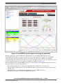
Figure 16. FreeMASTER control page for controlling the application
The basic control page is a part of the MCAT tool. The MCAT tool is a user-friendly graphical plug-in tool for
FreeMASTER, which enables you to easily tune and control motor-control applications. It supports up to three PMSM
motors and is fully compliant with the FOC cascade control structure. The added value of MCAT is the capability to
calculate the parameters of the PI controller in the control structure. All application parameters are stored and can be exported
as static configuration header file. For more details about MCAT see AN4642 (see References).
Monitor all application states using the PMSM control page, as shown in Figure 16. The Application State field displays the
actual state machine status. In case of the Fault state:
• The permanent/pending faults are indicated by a highlighted red bar with the name of the fault source.
• The actual faults are indicated by the circle-shaped LED-like indicator, which is placed next to the bar with the name of
the fault source.
• The actual presence of a fault is indicated by highlighting the respective LED-like indicator.
• The RUN button changes to FAULT and is highlighted by red color.
Dual 3-Phase PMSM Development Kit with MPC5643L, Rev. 1, 11/2015
Freescale Semiconductor, Inc.
27
Application Control User Interface
The example in Figure 16 shows a normal operating condition of the motor running under the speed control. Monitor the
real-time behavior of the phase currents using FreeMASTER recorder. There are no faults indicated in the example. If a fault
state occurs for any reason, the application switches off automatically, and displays the FAULT application state, indicated
by a pink frame indicator.
When all actual fault sources are removed (which is indicated by none of the LED-like fault indicators being lit), clear the
pending faults by pressing the FAULT CLEAR button that appears instead of the RUN button. This clears all pending faults
and enables the transition of the state machine into the INIT state and then to the READY state. Because INIT is a one-pass
state, FAULT-INIT-READY transitions happen so fast that they are not visible on the control page. It seems as if the state
machine went from FAULT to READY directly. This is not an error, it is caused by a slow communication via RS232, and/or
slow refresh rate of the control page.
When the application faults are cleared and the application is in the READY state, all variables are set to their default values.
Start the application by clicking the "On/Off" button.
In the RUN state, all control loops of the FOC algorithm are active. That means that the three-phase currents are measured
and used to close the current loop, and the actual rotor speed is measured to close the speed loop. Select the desired speed of
the rotor in the variable watch window. The variable for controlling the speed is called Nreq; it is the required speed
recalculated to the mechanical speed in revolutions per minute.
Switch the application off by clicking the On/Off button, and it proceeds to the INIT state and consequently to the READY
state. Because of the motor used, select the required speed in the range from -3000 rpm to 3000 rpm.
In the Dual PMSM application, you can control two motors independently. That means that you can call different states of
the state machine at once. Click the radio button in the motor selection bar of MCAT, and select and control either Motor#1
or Motor#2. The MCAT environment for a given motor is differentiated by color.
The field-weakening algorithm is not implemented, and the required value of the d-axis current is set to zero.
6.1 Application quick start
• Install the USB driver to create a virtual COM port for emulation of the RS232 communication. For example, “CP210x
USB to UART Bridge VCP Drivers” from www.silabs.com.
• Connect the USB cable to the MPC5643L controller board and to the host PC.
• Connect the power supply to the power stage. The controller board power supply is taken from the power stage. The
PMSMs in the development kit are designed for a phase voltage of 18 V.
• Start the FreeMASTER project located at: MPC5643L_SPMSM_Development_Kit\FreeMASTER_control
\MPC5643_Single_PMSM_MCAT.pmp, or MPC5643L_DPMSM_Development_Kit\FreeMASTER_control
\MPC5643_Dual_PMSM_MCAT.pmp.
• Enable communication by pressing the STOP button in the toolbar in FreeMASTER, or by pressing CTRL+K.
• Successful communication is indicated in the status bar of the FreeMASTER.
• If no actual faults are present in the system, all of the LED-like indicators shall be dark red. If there is a fault present,
identify the source of the fault and remove it. Successful removal is indicated by the switching off of the respective
LED-like indicator.
• If all of the LED-like indicators are off, clear the pending faults by pressing the FAULT CLEAR button.
• Start the application by pressing ON of the On/Off button.
• Enter the required speed by assigning this value to the M1.NmecReq or M2.NmecReq variable in variables watch
window, or use the appropriate speed gauge in the PMSM Control Page of Motor #1 or Motor #2. The value is in
revolutions per minute.
• Stop the application by pressing OFF of the On/Off button.
• Stop the application of both motors immediately by pressing the red-circled Central Stop button.
• RESET the application anytime by pressing the blue-circled H/W. RESET button.
Dual 3-Phase PMSM Development Kit with MPC5643L, Rev. 1, 11/2015
28
Freescale Semiconductor, Inc.
References
7 References
1.
2.
3.
4.
5.
6.
7.
8.
MPC5643L Microcontroller Reference Manual, MPC5643LRM, (http://www.fsls.co/doc/MPC5643LRM )
MPC5643L Controller Board User Manual, MPC5643LDMCBUM, (www.fsls.co/doc/MPC5643LDMCBUM )
FreeMASTER Run-Time Debugging Tool, (http://www.freescale.com/FREEMASTER )
MCLib for MPC564xL User Reference Manual, (http://www.freescale.com/AutoMCLib )
3-phase BLDC/PMSM Low Voltage Power Stage User Manual, www.fsls.co/doc/3PHLVPSUG
MC33937 Three Phase Pre-driver Data Sheet, http://www.fsls.co/doc/MC33937
AN4642, Motor Control Application Tuning (MCAT) Tool for 3-Phase PMSM (http://www.fsls.co/doc/AN4642 )
Motor Control Application Tuning (MCAT) Tool, (http://www.freescale.com/MCAT )
8 Revision history
This section documents the changes done to this document.
Table 2. Revision history
Revision
Date
Substantial changes
0
05/2012
Initial release.
1
11/2015
Updated Sections 1, 2, 4.1, 5.2, 6, 6.1, and 7.
Dual 3-Phase PMSM Development Kit with MPC5643L, Rev. 1, 11/2015
Freescale Semiconductor, Inc.
29
How to Reach Us:
Home Page:
freescale.com
Web Support:
freescale.com/support
Information in this document is provided solely to enable system and
software implementers to use Freescale products. There are no express
or implied copyright licenses granted hereunder to design or fabricate
any integrated circuits based on the information in this document.
Freescale reserves the right to make changes without further notice to
any products herein.
Freescale makes no warranty, representation, or guarantee regarding
the suitability of its products for any particular purpose, nor does
Freescale assume any liability arising out of the application or use of
any product or circuit, and specifically disclaims any and all liability,
including without limitation consequential or incidental damages.
“Typical” parameters that may be provided in Freescale data sheets
and/or specifications can and do vary in different applications, and
actual performance may vary over time. All operating parameters,
including “typicals,” must be validated for each customer application by
customer's technical experts. Freescale does not convey any license
under its patent rights nor the rights of others. Freescale sells products
pursuant to standard terms and conditions of sale, which can be found
at the following address: freescale.com/SalesTermsandConditions.
Freescale and the Freescale logo are trademarks of Freescale
Semiconductor, Inc., Reg. U.S. Pat. & Tm. Off. All other product or
service names are the property of their respective owners.
© 2015 Freescale Semiconductor, Inc.
Document Number AN4518
Revision 1, 11/2015