1
MOSES ADELERE
AN FPGA MUSIC PLAYER
TECHNOLOGY AND COMMUNICATION
2011
VAASAN AMMATTIKORKEAKOULU
UNIVERSITY OF APPLIED SCIENCES
Information Technology Degree Programme
ABSTRACT
Author
Title
Year
Language
Pages
Name of Supervisor
Moses Adelere
An FPGA Based Music Player
2011
English
55
Yang Liu
As the demand for portable electronics devices increase, so is the need for an
improved technology. Electronics manufacturers around the world are looking for
ways to make profit at a reasonable cost of production.
The objective of this thesis is to replace microcontroller based electronic devices
with an FPGA which eliminates the cost of acquiring new peripheral when new
functionality is to be added to existing devices.
The design is in two phases, mainly consisting the hardware and software. The
hardware modules use an Intellectual properties from Terasic Technology, excepts
the VGA display. The software module communicates with the Nios processor.
Keywords
FPGA, Microcontroller, Intellectual properties
ACKNOWLEDGEMENT
First and foremost, to Almight God for his guidance and wisdom all through the
years I have lived. To my mother for giving me life. To the rest of my family for
their support. To all my friends, who support and advise me all through my study.
To my supervisor, Liu Yang for his advise and support. To Jarmo Makela, who
made mathematics so simple, also not to forget Dr Gao Chao, a teacher of high
pedigree, and to the rest of the teacher in VAMK.
To Altera and Terasic, for giving the right to edit source code and other
intellectual propery of the company.
1
CONTENTS
ABSTRACT
ACKNOWLEDGEMENT ...................................................................................... 2
ABBREVIATIONS ................................................................................................ 3
1
INTRODUCTION ............................................................................................ 4
1.1 BRIEF INTRODUCTION ABOUT FPGA .............................................. 4
1.2 BENEFIT OF USING FPGA IN DESIGN ............................................... 4
2
DE2 EDUCATIONAL BOARD ...................................................................... 5
2.1 STRUCTURE OF THE DE2 BOARD ..................................................... 6
3
DEVELOPMENT SOFTWARE ...................................................................... 9
3.1 QUARTUS II SOFTWARE ..................................................................... 9
3.2 SOPC BUILDER .................................................................................... 11
3.3 NIOS II EMBEDDED DEVELOPMENT IDE ...................................... 12
4
BACKGROUND ABOUT THE SYSTEM REQUIREMENT ...................... 13
4.1 WAV FORMAT ..................................................................................... 13
4.2 FAT FILE SYSTEM ............................................................................... 16
4.2.1 STRUCTURE OF THE FAT16 FILE SYSTEM ........................ 18
4.3 WM8731 AUDIO CODEC ..................................................................... 19
4.4 SD CARD ............................................................................................... 22
4.5 ADV7123 VGA CODEC ........................................................................ 23
5
IMPLEMENTATION .................................................................................... 25
5.1 SD CONTROLLER ................................................................................ 28
5.2 AUDIO CONTROLLER ........................................................................ 31
5.3 VGA CONTROLLER ............................................................................ 34
5.4 FAT FILE LIBRARY ............................................................................. 45
5.5 WAVE LIBRARY .................................................................................. 48
5.6 OTHER PERIPHERALS ........................................................................ 50
5.7 USER CONTROL .................................................................................. 51
5.8 FUNCTIONAL DIAGRAM ................................................................... 52
5.9 PROBLEM FACED................................................................................ 53
5.10 FUTURE WORK .................................................................................... 54
2
6
CONCLUSION .............................................................................................. 54
REFERENCE ........................................................................................................ 55
3
ABBREVIATIONS
FGPA
Field gate programmable array
I2C
Inter integrated circuit
FAT
Fat allocation table
SD
Secure digital
SOPC
System on programmable chip
RIFF
Resources interchange file format
JTAG
Joint test action group
UART
Universal asynchronous receiver/transmitter
HDL
Hardware description language
VHDL
VHSIC Hardware description language
VHSIC
Very high speed integrated circuit
DAC
Digital to analog converter
4
1
INTRODUCTION
The aim of this thesis is to build an FPGA based music player. Firstly, the word
FPGA is an acronym for “Field programmable gate array” which is an integrated
circuit designed to be configured by the designer after being manufactured. The
configuration of an FPGA can be done using HDL and C programming language
provided it has a custom program inbuilt processor like in Altera FPGA used for
the implementation of this project.
Altera defines FPGA ha a semiconductor device that can be programmed after
manufacturing, and allow you to program products features and functions, adapt
to new standards, and reconfigure hardware for specific applications even after the
product has been installed on the FPGA [5].
1.1
BRIEF INTRODUCTION ABOUT FPGA
The manifestation of the FPGA industry began from PROM (programmable read
only memory) and PLD (programmable logic device). Both of which can be
programed in batches from the factory.
In 1984, the first FPGA device was invented by Ross Freeman, also the cofounder of the Xilinx technology. The first design was “XC2064” chip, is a
computer chip full of open gates that engineers can reprogram as much as the
need arises to add a new functionality to custom device, and the adaptation to
changing specification.
1.2
BENEFIT OF USING FPGA IN DESIGN
The following benefits can be derived from using FPGA chips in electronics
designs.
5
1. Good performance
considering the advantage derived from hardware parallelism, FPGA exceeds
the computing power of digital signal processing [10].
2. Customization
This option provides the designer of electronics system the flexibility to
choose the desire components, controllers and peripherals to be used in
designs.
3. Component and cost reduction
With the vast capability of FPGA, previous system designs that required
additional components to improve its functionality can be replaced with a
single FPGA chip. The reduction in the number of components in a design
can reduce the robust size of the board and inventory management, thus
reduce the time expended and also cut down the cost of production.
4. Obsolescence mitigation
FPGA soft-processor provides an excellent solution that arises when
considering the lifespan of electronics designs. Since the source of HDL
for the soft-processor can be purchased from it owner to combat the issue
of component obsolescence mitigation.
2
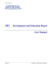
DE2 EDUCATIONAL BOARD
The information about the DE2 educational board is an extract from the user
manual provided by Altera on the board.
6
2.1
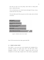
STRUCTURE OF THE DE2 BOARD
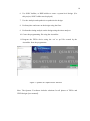
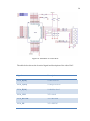
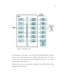
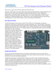
The figure below shows a labelled diagram of the DE2 educational board,
illustrating its layout, and indicating the component constituting the board.
Figure 1: DE2 Educational Board [5]
The board has many features, allowing end-user to implement a wide range of
embedded application ranging from the simple to sophisticated circuits.
The board is equipped with the following hardware;
-
Altera cyclone II 2C35 FPGA device
-
Altera serial configuration device – EPCS16
7
-
USB Blaster for programming and user API control, both JTAG
and Active serial programming modes are supported
-
512-Kbytes SRAM
-
8-MByte flash memory
-
SD Card socket
-
Four user push-button switches
-
18 Toggle switches
-
18 Red user LEDs
-
9 Green user LEDs
-
50-MHz and 27-MHz Oscillator for clock sources
-
24-bit CD quality audio CODEC with line-in, line-out, and
microphone in-jacks
-
VGA DAC (10-bits high speed triple DACs) with VGA-out
connector
-
TV decoder (NTSC/PAL) and TV-in connector
-
10/100 Ethernet controller with a connector
-
USB Host/Slave controller with USB type A and B connector
-
PS/2 mouse/keyboard connector
-
IrDA transceiver
-
Two 40-pins Expansion headers with diode protection
Also with the above hardware, the board is also equipped with software examples.
The board requires its users to be familiar with Quartus II software before the
8
FPGA chip can be programmed, and in some case the requirement is not only the
Quartus II software, but also the NIOS II software.
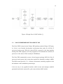
The figure below shows the block diagram of the DE2 board.
Figure 2: Block diagram of the DE2 board.[x1]
9
3
DEVELOPMENT SOFTWARE
In this section of the report, the software used for the implementation of the
project will be described in short detail.
3.1
QUARTUS II SOFTWARE
The software was developed by Altera technology for programming FPGA device
using HDL programming, Block diagram/schematic files, or others design entry
formats. it has an easy to use graphical user interface, and a modular complier
which includes the following lists below;
1. Analysis and synthesis
2. Fitter (place and route)
3. Assembler (generates the programming file)
4. Timing Analysis
5. EDA Netlist Writer.
The following procedure describe how to create a new project on the Quartus II
graphical interface
1. Launch the software from your computer
2. Create a new project, select File → New project wizard
3. Choose the device family (for this project cyclone II)
4. Using the Text editor, create a new HDL file (Verilog/VHDL), or Block
editor to create clock diagram with symbols representing the design.
5. Use the MegaWizard Plug-in manager to generate custom variations of
megafunctions and IP functions to instantiate the design. (Optional)
10
6. Use SOPC builder, or DSP builder to create a system-level design. (For
this project, SOPC builder was deployed)
7. Use the Analysis and synthesis to synthesize the design
8. Perform place and route on the design using the fitter.
9. Perform the timing analysis on the design using the timer analyser
10. Create the programming file using the Assembler
11. Program the FPGA device using the .sof or .pof file created by the
Assembler from the programmer.
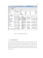
Figure 3: Quartus II Graphical user interface
Note: The Quartus II software includes solutions for all phases of FPGA and
CPLD designs [user manual].
11
3.2
SOPC BUILDER
The SOPC builder is one among the system-level design flow supported by the
Quartus II software. It is included in the Quartus II software, and allows engineers
to rapidly design and evaluates system-on-chip architecture, as well as design at a
higher level of abstraction.
The SOPC builder is an automated system development tools that dramatically
simply the task of creating a high-performance SOPC designs [user manual].it
provides engineers the opportunity to design a custom component, use SOPC
system component in design architectures, as well as generate and verifying the
system before final integration of the system. It composed of components such as
CPU, memory, timer, standard and user-define peripheral, UART, JTAG, Avalon
tri-state bridge etc., and also provide an interface to user-defined logics. There are
four techniques for using SOPC builder system with user-defined logic;
1. Simple PIO connection
2. Bus interface to external logic
3. Publishing a local SOPC builder component, and
4. instantiation inside the system module
For each project created with the SOPC builder contains a system descriptive file.
The file which has a .ptf extension contains all the options, setting, and parameter
included in the SOPC builder. Each component included in the SOPC design has a
corresponding PTF file, and this file is used in generating the source code,
software component and simulation files for the system.
The design flow of a typical SOPC builder is shown below;
12
Figure: 4 Design flow of SOPC builder [].
3.3
NIOS II EMBEDDED DEVELOPMENT IDE
The Nios II IDE is based on the Eclipse IDE platform, and the Eclipse CDT plugin. It has a user friendly development environment that works for all Nios II
processor based system. With the Altera FPGA connected to the host machine
running Nios IDE, engineers can write program for and communicate with Nios II
processor via the Altera JTAG usually the USB Blaster.
The Nios EDS automatically creates a board support package (BSP) for Nios II
processor based system, thus saving time required for manually creating it (BSP).
The BSP created provide C/C++ runtime environment, insulating engineers from
the hardware in the embedded system design.
It has an easy to use graphical interface which creates and manages makefile
generated based on the system file (.ptf) create with the SOPC builder.
13
4
BACKGROUND ABOUT THE SYSTEM REQUIREMENT
The following heading gives an insight about the major entity of the system.
4.1
WAV FORMAT
The Wav file format is part of the numerous formats defined in the Microsoft
RIFF specification for storing media files. It can be identified by the extension in
its filename (.wav). The type of data samples stored is the raw data without any
form of compression making it relatively large compared to other media format
like the MPEG.
It consists of three chunks of information namely;
1. RIFF (Resource interchange file format)
2. Format
3. Data
The RIFF is a tagged file structure developed for multimedia resources files. Its
structure is very similar to the Electronic Art IFF, though not a file format in its
own natural existence, but contains “Interchange file format” related to its origin.
As a chunk, it identifies the file as a Wav file making it suitable for;
1. playing back multimedia data
2. recording multimedia data
3. Exchanging multimedia data between applications.
The format chunk identifies parameters such as numbers of channel, sample
rates etc., while the Data chunk contains the actual data sample of the media
file. The figure below show a Wav file format block;
14
Figure 5: A Canonical Wav file format [4]
The table below gives an insight about the wav file format
Offset
Name
Size (Bytes)
Description
0
ChunkID
4
Contains
the
letters “RIFF” in
ASCII
format
(0x46464952
little-
endian
form).
4
ChunkSize
4
4
+
(8
+
15
subchuk1Size)
+
(8
+
SubChunk2Size)
8
Format
4
Contains the letter
“WAVE”
(0x45564157
little-endian form)
12
Subchunk1ID
4
Contains the letter
“fmt”
(0x20746d66
little-endian form)
16
Subchunk1Size
4
16 for PCM
20
AudioFormat
2
PCM = 1, other
values indicate a
form
of
compression
in
the data
22
NumChannels
2
Mono = 1, Stereo
=2
24
SampleRate
4
8000, 44100 etc.
28
ByteRate
4
SampleRate
*
NumChannels
*
BitsPerSample/8
32
BlockAlign
2
The
number
bytes
for
of
one
sample including
16
all channels.
36
Subchunk2ID
4
Contains
letters
the
“data”
(0x61746164
little-endian
form).
40
Subchunk2Size
4
This is the number
of bytes in the
data sample.
44
Data
no specific size
The actual sound
data.
Table 1: Wave Data information [4]
4.2
FAT FILE SYSTEM
The FAT is an abbreviation of File Allocation Table, designed by Microsoft
giving operating systems the possibility to track the location and determine the
order of succession of each pieces of a file. Since the inception of the common
removable flash memory, the FAT system has become a format widely used file
format in digital device, computers.
The FAT file system provides a way of tracking and monitoring when a file is
created or updated, and identifying the size of the file. It also provides mechanism
for storing other characteristics of a file such as read-only, whether a hidden in a
directory display making it an ideal file format for removable memory devices.
The table below provides information about the structure of the FAT file system;
17
Byte Offset
Length (Bytes)
Description
0x00
3
jump instruction to boot
code
0x03
8
indicates
what
system
formatted the volume
0x0B
2
number
of
bytes
per
sector
0x0D
1
number of sector per
cluster
0x0E
2
number
of
reserved
of
allocated
sector
0x10
1
number
tables
0x11
2
maximum number of root
directory entries
0x13
2
total number of sector
0x15
1
media descriptor
0x16
2
sectors per FAT
0x18
2
sectors per track
0x1A
2
Numbers of heads for
interrupt 0x13.
0x1C
4
count of hidden sectors
preceding the partition
18
4
0x20
This field is the new 32bit total count of sectors
on the volume.
Table 2: Common offset among versions of FAT file system [1]
4.2.1
STRUCTURE OF THE FAT16 FILE SYSTEM
The FAT system disk is organised into sectors, with each sector storing 512 bytes
of data. The sector is the smallest unit used when writing or reading data from
disk formatted with the FAT system. Unlike the sector, the cluster is used by the
operating system as the smallest unit when allocating storage space on disk with
FAT partition, having a variying size depending on size of the partition, and
varies from drive to drive.
The FAT identifies each cluster in a partition as;
1. Cluster in-use by a file
2. Bad cluster
3. Unused cluster
4. Last cluster in a file
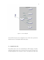
FAT16 file system uses 16 bits cluster addressing system, and its volume is
divided into four as shown in Figure 6 below.
The boot sector is the first sector of the volume, defining the volume, and also
contains the code to enter the file system.
The FAT is a series of addresses for checking the next cluster in the system,
and accessed as a lookup table. The FAT is an important data structure such
19
that it has two copies, one as the primary, and the other as a backup when
there is a fault in the system.
The root folder/directory has a fixed location and length (512 bytes), always
located at the start of the volume.
The other folders and all files occupy the rest of the volume, and are divided
into clusters.
Figure 6: Structure of the FAT16 volume
Note: FAT16 can not be used on volume greater than 2GB.
4.3
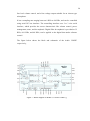
WM8731 AUDIO CODEC
The CODEC is a low power stereo codec integrated with a headphone driver,
specifically designed for portable audio device such MP3 player, PDAs,
smartphone, recorders etc. The CODEC is equipped with stereo line and
microphone level audio inputs, alongside with a mute function, programmable
20
line level volume control, and a bias voltage output suitable for an electret type
microphone.
It has a sampling rate ranging between 8 KHz to 96 KHz, and can be controlled
using serial I2C bus interface. The controlling interface uses 2 or 3 wire serial
interface, which provides the access characteristic like volume control, power
management, mute, and de-emphasis. Digital filter de-emphasis is provided at 32
KHz, 44.1 KHz, and 48 KHz, can be applied to the digital data under software
control.
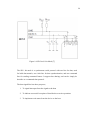
The figure below shows the block and schematic of the Audio CODEC
respectively;
Figure 7: Block diagram of WM8731 Audio CODEC []
21
The CODEC includes a crystal oscillator circuit which allows audio system
reference clock to be generated on device. The oscillator is designed for low EMI,
and radiation type. In buffered form, it is available to the rest of the audio system
on CLKOUT.
In Digital audio interface, it can be operated in any of the 4 mode offer. These are;
1. I2C
2. DSP
3. Right justified
4. Left justified
The entire modes have a common characteristic of MSB first, and operate with
data 16 to 32 bit; also the DACLRC and ADCLRC must always change on the
falling edge of the BCLK. Only the Right justified does not supports 32 bits data.
22
Figure 8: Schematic diagram of Audio CODEC
4.4
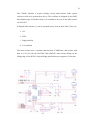
SD CARD
The SD Card known as the secure digital card was design to cater for the need for
reliable data storage on consumer mobile and portable electronics, such as digital
camera, mobile phones, etc. it was design by the SD Card association. All SD
Card supports Microsoft FAT16 file system.
The SD Card can be accessed via a dedicated serial interface for fast data
transmission. The interfacing buses are:
1. SPI
2. SD 1-bit mode
3. SD 4-bit mode
23
Figure 9: SD Card Architetcture [8]
4.5
ADV7123 VGA CODEC
The ADV7123 is triple high speed, digital-to-analog converter on a single
monolithic chip [4]. It has three 10 bit input ports, 5V/3.3V power supply, and
requires clock input for full functionality. Also include in the ADV7123 is an
additional control signals, composite SYNC and BLANK. Its applications can be
seen in the following;
1. Video signal reconstruction
2. Instrumentation
3. Digital radio modulation
4. Image processing
5. High resolution colour graphic
6. Digital video systems
The figure below show the schematic diagram of the ADV7123 video DAC
connected to the VGA port.
24
Figure 10: Schematic of Video DAC
The table below shows the electrical signal and description of the video DAC.
Signal name
Description
VGA_R[9:0]
10-bit red level
VGA_G[9:0]
10-bit green level
VGA_B[9.0]
10-bit blue level
VGA_CLK
VGA clock
VGA_BLANK
VGA BLANK
VGA_HS
VGA HSYNC
25
VGA_VS
VGA VSYNC
VGA_SYNC
VGA SYNC
Table 3: Signal assignment of ADV7123
5
IMPLEMENTATION
The implementation for the system requirement of this project is divided into two
parts;
1. Hardware
2. Software
which the SOPC builder uses the Avalon switch fabric as the connecting bridge
between the hardware and the software. Avalon switch fabric is a collection of
signals and logics that connects master and slave of the SOPC builder and other
custom components in a Nios II system development.
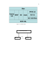
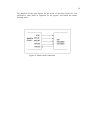
The block diagrams below hardware and software stack for the project;
26
Figure 11: Software stack
System Requirement
Hardware
SOPC
Software
27
Figure 12: Hardware stack
In the hardware development, I used the SOPC builder components and other
custom or user defined components to configure and generate the Nios system.
For the software development, the Nios embedded design suite was used to
communicate with the processor.
The figure below shows the hardware connection in the SOPC builder for the
implementation of the project.
28
Figure 13: SOPC Builder connection
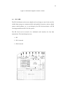
5.1
SD CONTROLLER
In the software stack diagram, the SD Card was used to store the music file which
was read by the Nios II processor. The main operation of the SD Card was
implemented in the software phase using the SD 1 bit mode of operation; in the
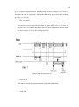
hardware phase four PIO pins were connected to the SD Card socket. Figure 14
below shows the hardwire connection between the SD card in SD 1-bit mode and
the host device.
29
Figure 14: SD Card 1-bit Mode [7]
The SD 1 bit mode is a synchronous serial protocol with one line for data, used
for bulk data transfer, one clock line for data synchronisation, and one command
line for sending command frames. It support bus sharing, and can be simply be
describe as a command-data protocol.
The data signal/line has three purposes;
1. To signal interrupts from the signal to the host
2. To indicate successful reception of data blocks on write operations
3. To implement wait states from the device to the host
30
In the software implementation, the following function prototype were used to
configure the card in 1-bit mode. This means that it will only read a block of data
at a time i.e. 512 byte.
1. SD_read_block
This function read a single block of data at a time whose size is 512 byte. It
sent the cmd17 to read the data on the SD card, then synchronise the data with
the clock. Figure 15 shows the reading operation.
Figure 15: Read operation [6]
2. response_R
This function return the response related to the command issued.
3. send_cmd
31
This function sends command to the SD card.
4. SD_card_init
This function function initialises and detects the card. It persistently sends
command to the card, and waits until the response is a success. An example of
the response is the CRC.
The command sent in this function is in the following sequence;
cmd55
cmd41
cmd2
cmd3
cmd9
cmd10
cmd7
cmd16
The hardware peripheral as used in the SOPC builder for the wiring the SD
card uses four parallel input/output (PIO) peripheral. The PIOs are SD_CLK,
SD_DAT, SD_DAT3, SD_CMD. The SD_CLK has data width of 1,
directional port is set to output, and the port direction reset value is 0x0. The
SD_DAT, SD_CMD, and the SD_DAT3 has a data width of 1, direactional
port is set to bidirectional tristate, and the port direction reset value is 0x0.
5.2
AUDIO CONTROLLER
The Audio controller used is a user-defined SOPC component from Terasic
technology. It needs an input clock of 18.432 MHz which was generated using
PLL, and the resulting clock fed to the Audio controller was 18.51 MHz. The
audio configuration demands that the controller operates in the master mode, so
that the serial bit (BCK) and the left/right channel clock were provided by the
audio chip. The master mode was enabled in the software with the function below;
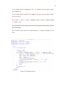
Bool audio_init(void){
Bsuccess = audio_regwrite(7, 0x0042);
}
32
The function set the data register for the mode of operation which I2C was
preffered to other mode of operation for the project, and enable the master
clocking mode.
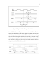
Figure 16: Master mode connection
33
Figure 17: Digital Audio Data Timing – Master Mode
In the SOPC builder, two PIO pins were connected to the I2C bus. This bus
protocol was implemented in the software module to configure the audio chip
with 16-bits per channel. In this mode, the MSB is available on the second rising
edge of the BCLK following the transition in the DACLRC or ADCLRC. Figure
19 below gives an insight. The audio data fetched from the SD card is always 512
bytes, and will be written to the DAC FIFO of the audio controller. Before the
writing, it checks if the FIFO buffer is not full.
34
Figure 18: I2S mode of operation
The I2C bus consists of two wires and a ground connection. The two wires are
I2C_SCLK which has a data width of 1, port direction is set to output, and port
Figure 19: Two wire I2C mode
direction reset value of 0x0, and the I2C_SDAT which has a bi-direction port,
data width of 1, and port direction reset value of 0x0.
5.3
VGA CONTROLLER
The standard VGA format of a monitor contains 640 columns by 480 rows of
picture elements. These elements are referred to as pixels, performing the function
of displaying images on the screen of the monitor by turning ON and OFF of
individual pixel.
The VGA monitor uses five control signals: RED, GREEN, BLUE, HSYNC, and
VSYNC. The first three control signals are commonly referred to as RGB signal,
controlling the colour formation of a pixel at any location on the screen of the
monitor. These signals are carried by the VGA connector to the VGA port of the
host. The signals are analog signal with voltage level ranging from 0.7 to 1V.
35
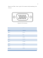
Figure 14 and Table 3 show a typical VGA connector and pin numbering of the
connector.
Figure 20: VGA Connector
Pin 1
RED
pin 2
GREEN
pin 3
BLUE
pin 4
ID2
pin 5
GND
pin 6
RGND
pin 7
GGND
pin 8
BGND
pin 9
+5V
pin 10
GND
36
pin 11
ID0
pin 12
ID1
pin 13
HSYNC
pin 14
VSYNC
pin 15
ID3
Table 4: Pin numbering of VGA Connector
To achieve different colour combinations, the RGB signal voltage have to be
varied. The text color on the VGA display for this project is white as can be seen
in Figure 15 below. This shows that the RGB signals are high. Table 4 show the
Table 5: Color combination
voltage level of the signal to achieve 23 different color combinations.
37
The VGA timing requirement is an important parameter that was considered when
implementing the VGA controller circuit. The timing parameters for the display
are 640 x 480 resolutions, a 25.175 MHz clock, 31.469 KHz Line Frequency, and
59.94 Hz Field Frequency.
Pixels
Role
8
Front porch
96
Horizontal Sync
40
Back Porch
8
Left border
640
Active
8
Right border
800
total/line
Lines
Role
2
Front porch
2
Vertical Sync
25
Back porch
8
Top Border
38
480
Active
8
Bottom border
525
total/field
Table 6 and 7: Horizontal and vertical sync signals
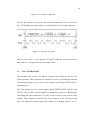
The values in table 5 and 6 were used for the horizontal and vertical scanning of
the screen at a refreshing rate of 60 Hz. The horizontal and vertical scanning uses
a counter for its implementation which can be seen in the screenshot below. The
total horizontal is 800, and that of the vertical is 525.
39
Figure 21: Horizontal and vertical counter
The VGA timing table shown in Table 7 is derived from 640 x 480 resolutions
using the clock of 25.175 MHz.
40
Table 8: VGA Timing
Since the clock required for the resolution 640 x 480 need 25 MHz, and the board
provides a 50 MHz clock. I generate the 25 MHz using the VHDL code in the
screenshot below.
Figure 22: 25 MHz clock generation
The display raster was implemented using an 8 x 8 rom. An example of the rom
created for letter “V” is shown below;
01100110
41
01100110
01100110
01100110
01100110
00111100
00011000
00000000
Figure 23: VGA Display
The method used for the text displayed on the VGA is called “tile mapping”. The
texts are in predesigned patterns. An example for a pattern “TIME:” is shown
below;
42
0111111000111100011000110111111000000000
0001100000011000011101110110000000000000
0001100000011000011111110110000000011000
0001100000011000011010110111100000000000
0001100000011000011000110110000000000000
0001100000011000011000110110000000011000
0001100000111100011000110111111000000000
0000000000000000000000000000000000000000
The update of the data displayed on the VGA screen is done both in the hardware
and software. In the software, I used the function IOWR (VGA_0_BASE,
ADDRESS, PARAMETER), and for the hardware update, bit mapping method
was employed. The process involves creating a tile memory, example an 8 x 80
rom for numerical values shown below, and each ascii bit on the VGA display
gets its bit from the memory.
001111000001100000111100001111000000011001111110001111000111111000
11110000111100
011001100001100001100110011001100000111001100000011001100110011001
10011001100110
011011100011100000000110000001100001111001111100011000000000110001
10011001100110
011101100001100000001100000111000110011000000110011111000001100000
11110000111110
43
011001100001100000110000000001100111111100000110011001100001100001
10011000000110
011001100001100001100000011001100000011001100110011001100001100001
10011001100110
001111000111111001111110001111000000011000111100001111000001100000
11110000111100
000000000000000000000000000000000000000000000000000000000000000000
00000000000000
The screenshot below shows the implementation of a single bit update for the
VGA.
Figure 24: Bit update process
44
This process was performed for every information (title of the song, sample rate,
time, and volume) displayed on the VGA monitor. Each of the character and
symbol displayed on the VGA monitor were given an address to make it
accessible to the Nios processor for update. The screenshot below gives an insight
how it was implemented in the VHDL code.
Figure 25: Bit addressing
Note: Using to_integer() gives a compilation error on Quartus V10, try to avoid it.
The address uses 5 bits which accommodate up to 32 addresses. The Nios uses
this addresses to update the information on the VGA monitor. An example is
shown in the screenshot below for updating the sample rate of the wav song.
45
Figure 26: Nios screen updating
5.4
FAT FILE LIBRARY
The FAT file library implement the FAT16 file system for reading wave file
stored in the SD Card. The FAT library support 8 characters long file name, and
only reads 512 bytes of data at a time.
The following functions implement the FAT library used in this project;
1. FatClusterType
This function identifies the cluster type in the FAT system. A cluster is a
group of sectors on memory devices that have at lease a piece of information
in it. The table below describe the FAT cluster type and their value or range as
used in the implementation.
FAT value
Description
0000h
Unused cluster
46
0002h-FFEFh
Used, Next cluster in file
FFF0h-FFF6h
Reserved cluster
FFF7h
Bad cluster
FFF8h-FFFF
Used, Last cluster in file
Table 9: Cluster Types [9]
The screenshot below shows how the FAT cluster type was implemented.
Figure 27: Cluster type
2. Fat_Dump
This function checks the directory created by the FAT system, and fetch out
information like name of the file in the directory, date created, attributes of the
file e.g hidden file, read-only, system file, volume of the file and so on.
47
3. Fat_ComposeFilename
This function was used to fetch the name and the extension type of the file in
the directory of the FAT system. The FAT system supports 8.3 filename
system i.e. 8 bits for the file name and 3 bit for its extension type. The figure
below shows how it was implemented in the Nios C code.
Figure 28: File name compose
4. Fat_FileSize
This function returns the size/volume of the file in the directory.
5. FatNextCluster
This fuction check the status of thr next clusters of the data. The pseudo-code
below describes the flow of the implementation.
1. if status is readonly
2. Nextcluster = *(unsigned
+(ThisCluster << 1));
short
*)(gVolumeInfo.szFatTable
3. ClusterType = fatClusterType(NextCluster);
4. check if type is not next in file and not last in file {NextCluster = 0}
48
5. else
6. nFatEntryPerSector = gVolumeInfo.BPB_BytsPerSec/nFatEntrySize;
7. sector
=
gVolumeinfor.FatEntrySector
(ThisCluster*nFatEntrySize)/gVolumeInfo.BPB_BytsPerSec;
+
8. read data block from SD Card
9. NextCluster
=
*(unsigned
short
(ThisCluster%nFatEntryPerSec)*nFatEntrySize);
*)(szBlock
+
10. go to 4
11. exit
6. Fat_FileCount
This function was used to count the number of files in the FAT directory.
The implementation is shown below;
Figure 29: File counting in the FAT system
5.5
WAVE LIBRARY
The WAVE library implements the decoding and retrieving of audio signal from
the wave file. The code implementation will be seen in the Appendices.
49
The following function implements the wave format used in the project.
1. Wave_IsWaveFile
This function check the format of the file stored in the SD card.
The
algorithm used is shown with the screenshot below.
Figure 30: Wave_IsWaveFile
2. Wave_GetSampleRate
The function returns the sample rate of the music file. Ths screenshot below
shows the algorithm.
Figure 31: GetSampleRate
50
3. waveGetChunkOffset
This function is returns the offset value of the wav format. The offset value
contains the necessary information of the wav format, that is why this function
is important to other functional implementation of the wav format as can be
seen in the code above. The implementation can be seen below:
Figure 32: waveGetChunkOffset
5.6
OTHER PERIPHERALS
The DE2 board provides a 2 x 16 LCD module, which display the name of the
music currently playing, and the volume of the player. The LCD module is an
SOPC builder component which was included into the project. The LEDs display
the strength of the audio signal which I called an equaliser. The LEDs module was
included into the SOPC builder as a PIO component, which includes 9 PIOs for
the green LEDs, and 18 PIOs for the red LEDs; both having an output direction
port.
The timer is another SOPC component used in the project. The project includes
two interval timer components from the SOPC library. The timers have 1
51
milliseconds period, with a counter size of 32 bits, with enabled writable period,
readable snapshot, and start/stop control bit.
The SDRAM controller provides the memory for the Nios system. The SDRAM
has a data width of 16 bits, address width with a row of 12 bits and column of 8
bits.
The Flash memory interface is also an important SOPC component. It has a data
width of 16 bits, and address width of 22 bits. It was used in the SOPC builder
system to provide memory for the system.
The SRAM module used in the SOPC builder is a user defined component, also
providing an altaernative memory for the processor. It has an address width of 18
bits, and a data width of 16 bits.
The CPU module provides the arithmetic logic unit for the system. It uses the 32
bit RISC architetcture, and runs at 100MHz clock speed which was provided
using the Altera PLL generator.
The Phase lock loop (PLL) module was used to set the required clocking for the
system. It takes an input clock of 50 MHz, to generate a clock of 100 MHz for the
CPU and other components, with the exception of the Audio controller which
runs at a clock of 18.432 MHz.
The JTAG UART module provides the communication interface between the host
PC and the SOPC builder system. It eliminate the need for a separate RS-232
connection.
5.7
USER CONTROL
User control is provided with four key buttons and two switches. The key buttons
and the switches were connected using the PIOs in the SOPC builder.
52
The buttons perform the different functions; the rightmost button is used to reset
the program on the DE2 board, two middle buttons were used to increase and
decrease the audio volume, leftmost for increasing and the rightmost for
decreasing. The last, leftmost button was used to play next track song on the SD
card.
Each of the switches used for this project performs two different functions, since
it can go back and forth. The first switch SW [0] is used to either continuously
repeat the current playing song from the SD card or leave it as a free playing
music player i.e. plays all the song stored in the SD card and go back to the first
track. The second switch, SW [1] was used to either play or pause the music in the
card.
5.8
FUNCTIONAL DIAGRAM
The use case diagram below shows the benefits the user of the music player will
derived from application.
53
Figure 33: Use case diagram
After the FPGA chip have been configured, the user will be able to perform the
functions in the use case diagram with the music player.
5.9
PROBLEM FACED
The problem faced at first was understanding the HDL language. Secondly,
making the display interface most of the time used in the project, because I have
no good background or prior experience. Firstly, I was using the 100 MHz clock
54
for the clock input, instead of the 50 MHz which was processed in the VHDL
implementation of the display to generate a 25 MHz used for the 640 x 480
resolution display of the VGA. When the project was first ran, I found that the
audio out was too fast resulting in a humming output. This was caused by the
crystal clock not been connected in the HDL used for the custom component.
5.10 FUTURE WORK
After the completion of the project, I planned to make a video game with the DE2
educational board preferable a soccer game, and a chat application.
6
CONCLUSION
In this project I have create a music player on an FPGA chip. The target of the
project in the beginning was achieved.
The Altera DE2 Education board is a good starting point to learn how to program
an FPGA. Altera already provides software tool like Quartus II, SOPC builder,
and Nios EDS as the programming IDE for the FPGA.
55
REFERENCE
1. Dave Dittrich. http://staff.washingtom.edu/dittrich
2. Microsoft. http://www.microsoft.com/about
3. Mcgill. http://www.mmsp.ece.mcgill.ca
4. Analog Device. http://www.analog.com
5. Altera. http://www.altera.com
6. Terasic. http://www.terasic.com
7. http://downloads.amilda.org/MODs/SDCard.SD.pdf
8. http://alumni.cs.ucr.edu/~amitra/sdcard/ProductManualSDCardv1.9.pd
f
9. http://home.teleport.com/~binary/fat16.htm
10. National instrument. http://zone.ni.com/devzone/cda/tut/id/6984
11. Wolfson microelectronics. http://www.wolfsonmicro.com