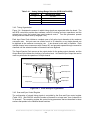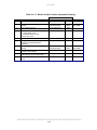
1
Rev: 090406
PMC-12AIO
12-BIT PMC ANALOG INPUT/OUTPUT BOARD
With 32 Input Channels, 4 Output Channels,
And 16-Bit Digital Port
_______________________
REFERENCE MANUAL
________________________________________________________________________________________
General Standards Corporation Ph:(256)880-8787 FAX:(256)880-8788 Email: [email protected]
MAN-PMC-12AIO
PCI-12AIO
Copyright (C) 2005 General Standards Corp.
Additional copies of this manual or other General Standards Co. literature may be obtained from:
General Standards Corp.
8302A Whitesburg Dr.
Huntsville, Alabama 35802
Telephone: (256) 880-8787
FAX:
(256) 880-8788
The information in this document is subject to change without notice.
General Standards Corp. makes no warranty of any kind with regard to this material, including, but not limited to, the implied warranties of
merchantability and fitness for a particular purpose. Although extensive editing and reviews are performed before release to ECO control,
General Standards Corp. assumes no responsibility for any errors that may exist in this document. No commitment is made to update or keep
current the information contained in this document.
General Standards Corp. does not assume any liability arising out of the application or use of any product or circuit described herein, nor is any
license conveyed under any patent rights or any rights of others.
General Standards Corp. assumes no responsibility resulting from omissions or errors in this manual, or from the use of information contained
herein.
General Standards Corp. reserves the right to make any changes, without notice, to this product to improve reliability, performance, function, or
design.
All rights reserved.
No part of this document may be copied or reproduced in any form or by any means without prior written consent of General Standards Corp.
General Standards Corporation Ph:(256)880-8787 FAX:(256)880-8788 Email: [email protected]
PCI-12AIO
TABLE OF CONTENTS
SECTION
1.0
TITLE
_
PAGE
1-1
INTRODUCTION
1.1
General Description
1-1
1.2
Functional Overview
1-2
2.0
INSTALLATION AND MAINTENANCE
2-1
2.1
Board Configuration
2-1
2.2
Installation
2-1
2.2.1
Physical Installation
2-1
2.2.2
Input/Output Cable Connections
2-1
2.3
2-3
System Configuration
2.3.1
Analog Inputs
2-3
2.3.1.1
Single-Ended Inputs
2-3
2.3.1.2
Differential Inputs
2-4
2.3.2
Analog Outputs
2-5
2.3.2.1
Output Configuration
2-5
2.3.2.2
Loading Considerations
2-5
2.3.3
External Sync
2-6
2.3.4
Multiboard Synchronization
2-6
2.3.5
Bidirectional Digital Port
2-7
2.4
Maintenance
2-7
2.5
Reference Verification
2-8
2.5.1
Equipment Required
2-8
2.5.2
Verification and Adjustment
2-8
3.0
3-1
CONTROL SOFTWARE
3.1
Introduction
3-1
3.2
Board Control Register (BCR)
3-1
3.3
Configuration and Initialization
3-2
3.3.1
Board Configuration
3-2
3.3.2
Initialization
3-3
__________________________________________________________________________________________
General Standards Corporation Ph:(256)880-8787 FAX:(256)880-8788 Email: [email protected]
i
PCI-12AIO
TABLE OF CONTENTS (Continued)
SECTION
3.4
TITLE
Analog Input/Output Parameters
_
PAGE
3-3
3.4.1
Analog Voltage Range
3-3
3.4.2
Timing Organization
3-4
3.4.3
Scan and Sync Control Register
3-4
3.4.4
Rate Generators
3-5
3.4.4.1
Scan Rate Control
3-6
3.4.4.2
Generator Cascading
3-6
3.4.5
3.5
3.5.1
Multiboard Synchronization
Analog Input Control
Input Data Organization
3-7
3-8
3-8
3.5.1.1
Input Data Buffer
3-8
3.5.1.2
Data Coding Format
3-8
3.5.2
Input Data Buffer Control
3-9
3.5.3
Analog Input Function Modes
3-9
3.5.3.1
Differential Inputs
3-9
3.5.3.2
Single-Ended Inputs
3-10
3.5.3.3
Selftest Modes
3-10
3.5.4
Input Scan Timing
3-10
3.5.4.1
Conversion Rate
3-10
3.5.4.2
Scan Rate
3-10
3.5.4.3
Scan Clocking Source
3-11
3.5.5
3.6
3.6.1
Scanning Modes
3-11
Analog Output Control
3-11
Output Data Organization
3-11
3.6.1.1
Output Data Buffer
3-11
3.6.1.2
Data Coding Format
3-12
3.6.2
Output Data Buffer Control
3-12
3.6.3
Output Clocking Modes
3-12
3.6.3.1
Sequential Clocking
3-13
3.6.3.2
Simultaneous Clocking
3-13
3.6.3.3
Output Clock Source
3-13
__________________________________________________________________________________________
General Standards Corporation Ph:(256)880-8787 FAX:(256)880-8788 Email: [email protected]
ii
PCI-12AIO
TABLE OF CONTENTS (Continued)
SECTION
3.6.4
TITLE
_
Output Sync Modes
PAGE
3-13
3.6.4.1
Continuous Outputs
3-13
3.6.4.2
Data Bursts
3-13
3.6.4.3
Output Sync Source
3-14
3.6.5
Function Looping
3-14
3.6.5.1
Periodic Function Generation
3-14
3.6.5.2
One-Shot Functions
3-15
3.6.5.3
Multiple Burst Queue
3-15
3.7
Autocalibration
3-15
3.8
Bidirectional Digital Port
3-16
3.9
Interrupt Control
3-16
3.9.1
Local Interrupt Request
3-16
3.9.2
Enabling the PCI Interrupt
3-17
3.10
3.11
4.0
3-19
DMA Operation
Periodic Function Looping Examples
PRINCIPLES OF OPERATION
3-20
4-1
4.1
General Description
4-1
4.2
Analog Inputs
4-2
4.3
Analog Outputs
4-2
4.4
Rate Generators
4-3
4.5
Data Buffers and Transfer FIFO's
4-3
4.6
Autocalibration
4-3
4.7
Power Control
4-4
App A
Control Register Quick Reference
A-1
__________________________________________________________________________________________
General Standards Corporation Ph:(256)880-8787 FAX:(256)880-8788 Email: [email protected]
iii
PCI-12AIO
LIST OF ILLUSTRATIONS
FIGURE
TITLE
_
PAGE
1.1-1
Physical Configuration
1-1
1.2-1
Functional Organization
1-2
2.2-1
Input/Output Connector
2-3
2.3-1
Analog Input Configurations
2-4
2.3-2
Output Configurations
2-5
2.3-3
Line Loss Versus Load Current
2-6
2.3-4
Multiboard Synchronization
2-7
2.5-1
Reference Adjustment Access
2-9
3.4-1
Clock and Sync Organization
3-4
3.4-2
Cascaded Rate Generator Example
3-7
3.5-1
Multiboard Synchronization
3-7
3.6-1
Function Burst; Output Buffer Data Flow
3-14
3.6-2
Periodic Function; Output Buffer Data Flow
3-15
4.1-1
Functional Block Diagram
4-1
__________________________________________________________________________________________
General Standards Corporation Ph:(256)880-8787 FAX:(256)880-8788 Email: [email protected]
iv
PCI-12AIO
LIST OF TABLES
TABLE
TITLE
_
PAGE
2.2-1
System Connector Pin Functions
2-2
2.5-1
Reference Verification Equipment
2-8
3.1-1
Control and Data Registers
3-1
3.2-1
Board Control Register (BCR)
3-2
3.3-1
Configuration Operations
3-3
3.4-1
Analog Voltage Range Selection
3-4
3.4-2
Scan and Sync Control Register
3-5
3.4-3
Rate Generator Register
3-6
3.4-4
Rate Generator Frequency Selection; Fclk=24MHz
3-6
3.5-1
Input Data Buffer
3-8
3.5-2
Input Data Coding; 12-Bit Data
3-8
3.5-3
Input Data Buffer Control Register
3-9
3.5-4
Analog Input Function Selection
3-9
3.6-1
Output Data Buffer
3-12
3.6-2
Output Data Buffer Control Register
3-12
3.8-1
Digital I/O Port
3-16
3.9-1
Interrupt Control Register
3-18
3.10-1
Typical DMA Register Configuration
3-19
3.11-1
Summary of Periodic Function Examples
3-20
3.11-2
Continuous Periodic Function; Sequential Clocking
3-20
3.11-3
Continuous Periodic Function; Simultaneous Clocking
3-21
3.11-4
Burst Periodic Function; Simultaneous Clocking
3-21
3.11-5
Burst Periodic Function, Sequential Clocking
3-22
__________________________________________________________________________________________
General Standards Corporation Ph:(256)880-8787 FAX:(256)880-8788 Email: [email protected]
v
PCI-12AIO
SECTION 1.0
INTRODUCTION
1.1 General Description
The PMC-12AIO board is a single-width PCI mezzanine card (PMC) that provides high-speed
12-bit analog input/output capability for PMC applications. 32 analog input lines can be
configured either as 32 single-ended input channels or as 16 differential channels, and are
digitized at rates up to 1,500,000 conversions per second. Four single-ended analog outputs
can be clocked at up to 400KSPS per channel with optional accelerated scanning. The voltage
range for analog inputs and outputs is software controlled as ±2.5V, ±5V or ±10V. A 16-bit
bidirectional digital I/O port also is provided. The board is functionally compatible with the IEEE
PCI local bus specification Revision 2.2, and is mechanically and electrically compatible with the
IEEE compact mezzanine card (CMC) specification IEEE 1386. A PCI interface adapter
supports the "plug-n-play" initialization concept.
Power requirements consist of +5 VDC from the PCI bus in accordance with the PCI
specification, and operation over the specified temperature range is achieved with conventional
convection cooling. Specific details of physical characteristics and power requirements are
contained in the PMC-12AIO product specification.
Figure 1.1-1 shows the physical
configuration of the board, and the arrangement of major components.
NOTE: Representative configuration. Details may vary.
PMC HOST CONNECTORS
SYSTEM I/O CONNECTOR
PRINTED CIRCUIT BOARD
STANDOFF (4)
5.87“ (149 MM)
P1
PCI INTERFACE
ADAPTER
U1
2.91“ (74MM)
P2
ANALOG COMPONENTS
SHIELD
POWER
CONTROL
SECTION
P5
LOCAL
CONTROLLER
U2
Figure 1.1-1. Physical Configuration
The board is designed for minimum off-line maintenance, and includes internal monitoring and
autocalibration features that eliminate the need for disconnecting or removing the module from
the system for calibration. All system input and output connections are made through a single
68-pin, dual-ribbon front-access I/O connector. The analog outputs are set to zero-level
(midrange) during initialization.
__________________________________________________________________________________________
General Standards Corporation Ph:(256)880-8787 FAX:(256)880-8788 Email: [email protected]
1-1
PCI-12AIO
1.2 Functional Overview
Principal capabilities of the PMC-12AIO board are summarized in the following list of features:
32 Single-Ended or 16 Differential 12-Bit Scanned Analog Input Channels
4 Analog Output Channels, 12-Bit D/A Converter per Channel
16-Bit Bidirectional Digital Port with Two Auxiliary I/O Lines
Software-Selectable Analog Input/Output Ranges of ±10V, ±5V or ±2.5V
Independent 32K-Sample Analog Input and Output FIFO Buffers
1.5 MSPS Conversion Rate in Single-Channel Mode;
1.0 MSPS in Multichannel Mode (1.5 MSPS with optional Accelerated Scanning)
Multiple-Channel and Single-Channel Input Scanning Modes
300K Samples per Second per Channel Analog Output Clocking Rate
(400K Samples per second with Optional Accelerated Scanning)
Supports Waveform and Arbitrary Function Generation
Continuous and One-shot Output Modes
Two Independent Internal Rate Generators
Supports Multiboard Synchronization of Analog Inputs and Outputs
Internal Autocalibration of Analog Input and Output Channels
DMA Engine Minimizes Host I/O Overhead
The PMC-12AIO board contains four 12-Bit D/A converters, a 12-bit scanning A/D converter,
and a 16-Bit bidirectional port with two auxiliary I/O lines. A PCI interface adapter provides the
interface between the controlling PCI bus and an internal local controller (Figure 1.2-1). Gain
and offset correction of the analog input and output channels is performed by calibration DAC's
that are loaded with channel correction values during autocalibration
I/O
Conn
Analog
Inputs
32 S.E.,
16 Diff
Input
Buffer
Amps
Selftest
Switches
Analog
Mux
Input
Range
Control
12-BIT ADC
Loopback
Voltage
Reference
Vtest Out
Sync Input
8-Bit
Calibration
DAC’S
AI
Buffer
AO
Buffer
PCI
Conn
PCI
Interface
Adapter
Local
Controller
12-Bit
Output
DAC’s
(4)
I/O
Conn
Analog
Outputs
4 S.E.
Local Bus
Figure 1.2-1. Functional Organization
__________________________________________________________________________________________
General Standards Corporation Ph:(256)880-8787 FAX:(256)880-8788 Email: [email protected]
1-2
PCI-12AIO
The analog inputs are software-configurable either as 32 single-ended channels or as 16
differential signal pairs. Buffer amplifiers on all input lines eliminate multiplexer input switching
noise, and minimize crosstalk and input bias currents. A selftest switching network routes a
precision reference to the A/D converter during autocalibration, and also provides loopback
monitoring of all analog output channels. Analog input data accumulates in a 32K-sample
buffer until retrieved by the PCI bus.
Each of the four analog output channels contains a dedicated 12-bit D/A converter, offset and
gain calibration DAC's, and an output range control network. The board receives analog output
data from the PCI bus through a 32K-sample FIFO buffer.
Analog input scanning can be synchronized to the analog output sample clock, or the inputs and
outputs can be operated independently. Both the analog inputs and outputs can be
synchronized externally, and a hardware output permits multiple boards to be synchronized
together. An interrupt request can be generated in response to selected conditions, including
the status of the analog input and output data buffers.
__________________________________________________________________________________________
General Standards Corporation Ph:(256)880-8787 FAX:(256)880-8788 Email: [email protected]
1-3
PCI-12AIO
SECTION 2.0
INSTALLATION AND MAINTENANCE
2.1 Board Configuration
This product has no field-alterable configuration features, and is completely configured at
the factory for field use.
2.2 Installation
2.2.1 Physical Installation
To minimize the opportunity for accidental damage before installation, the board should be
stored in the original protective shipping envelope. System power must be turned OFF
before proceeding with the installation.
CAUTION:
This product is susceptible to damage from electrostatic discharge (ESD).
Before removing the board from the conductive shipping envelope, ensure
that the work surface, the installer and the host board have been properly
discharged to ground.
After removing the board from the shipping envelope, position the board with the shield and
standoffs facing the host (carrier) board, and with the I/O connector oriented toward the
front panel. Align the two PCI connectors located at the end of the board opposite the I/O
connector with the mating connectors on the host board, and carefully press the board into
position on the host. Verify that the PCI connectors have mated completely and that the
standoffs are seated against the host board.
Attach the board to the host with four 2.5 x 6.5mm panhead screws. Pass the screws
through the back of the host into the four mounting holes on the board. Tighten the screws
carefully to complete the installation. Do not overtighten.
2.2.2 Input/Output Cable Connections
System cable signal pin assignments are listed in Table 2.2-1. I/O connector P5 is
designed to mate with a 68-pin dual-ribbon connector, equivalent to Robinson Nugent
#P50E-068-S-TG. The insulation displacement (IDC) Robinson Nugent cable connector
accepts two 34-wire 0.050-inch ribbon cables, with the pin numbering convention shown in
Table 2.2-1 and in Figure 2.2-1. Contact the factory if preassembled cables are required.
__________________________________________________________________________________________
General Standards Corporation Ph:(256)880-8787 FAX:(256)880-8788 Email: [email protected]
2-1
PCI-12AIO
Table 2.2-1. System Connector Pin Functions
P5 ROW-A
PIN
SIGNAL
(DIFF ANALOG INPUTS)
P5 ROW-B
SIGNAL
(S.E ANALOG INPUTS)
PIN
SIGNAL
34
ANA INP00 HI
ANA INP00
34
ANA OUT00
33
ANA INP00 LO
ANA INP01
33
OUTPUT RTN
32
ANA INP02 HI
ANA INP02
32
ANA OUT01
31
ANA INP02 LO
ANA INP03
31
OUTPUT RTN
30
ANA INP04 HI
ANA INP04
30
ANA OUT02
29
ANA INP04 LO
ANA INP05
29
OUTPUT RTN
28
ANA INP06 HI
ANA INP06
28
ANA OUT03
27
ANA INP06 LO
ANA INP07
27
OUTPUT RTN
26
ANA INP08 HI
ANA INP08
26
VTEST
25
ANA INP08 LO
ANA INP09
25
VTEST RTN
24
ANA INP10 HI
ANA INP10
24
DIGITAL RTN
23
ANA INP10 LO
ANA INP11
23
AUX DIGITAL IN
22
ANA INP12 HI
ANA INP12
22
AUX DIGITAL OUT
21
ANA INP12 LO
ANA INP13
21
DIG IO 00
20
ANA INP14 HI
ANA INP14
20
DIG IO 01
19
ANA INP14 LO
ANA INP15
19
DIG IO 02
18
INPUT RTN
INPUT RTN
18
DIG IO 03
17
INPUT RTN
INPUT RTN
17
DIG IO 04
16
ANA INP16 HI
ANA INP16
16
DIG IO 05
15
ANA INP16 LO
ANA INP17
15
DIG IO 06
14
ANA INP18 HI
ANA INP18
14
DIG IO 07
13
ANA INP18 LO
ANA INP19
13
DIG IO 08
12
ANA INP20 HI
ANA INP20
12
DIG IO 09
11
ANA INP20 LO
ANA INP21
11
DIG IO 10
10
ANA INP22 HI
ANA INP22
10
DIG IO 11
9
ANA INP22 LO
ANA INP23
9
DIG IO 12
8
ANA INP24 HI
ANA INP24
8
DIG IO 13
7
ANA INP24 LO
ANA INP25
7
DIG IO 14
6
ANA INP26 HI
ANA INP26
6
DIG IO 15
5
ANA INP26 LO
ANA INP27
5
DIGITAL RTN
4
ANA INP28 HI
ANA INP28
4
SYNC OUTPUT
3
ANA INP28 LO
ANA INP29
3
DIGITAL RTN
2
ANA INP30 HI
ANA INP30
2
SYNC INPUT
1
ANA INP30 LO
ANA INP31
1
DIGITAL RTN
__________________________________________________________________________________________
General Standards Corporation Ph:(256)880-8787 FAX:(256)880-8788 Email: [email protected]
2-2
PCI-12AIO
ROW A
ROW B
PIN 34
P5
CONN
PWB
PIN 1
Panel Pin-view
Figure 2.2-1. Input/Output Connector
2.3 System Configuration
2.3.1 Analog Inputs
2.3.1.1 Single-Ended Inputs
Analog inputs can be configured either as 32 single-ended channels or as 16 differential
channels. The hardware input configuration must be acknowledged by the control
software, which configures the controller for either single-ended or differential operation.
Pull-down resistors are provided on all analog inputs. Table 2.2-1 provides separate pin
assignment columns for single-ended and differential input configurations.
Single-ended operation (Figure 2.3-1a) offers the maximum number of input channels, but
generally provides optimum performance only when the input signal sources either are
isolated from each other, or are common only to a single isolated signal return.
Single-ended inputs share a common input return that provides a return path for all inputs,
making isolation from other system grounds a critical issue. If the signal sources are
returned externally to system ground when operating in this mode, a potential difference
between the system ground and input return can cause erroneous measurements, or may
generate excessive ground current and damage the board.
__________________________________________________________________________________________
General Standards Corporation Ph:(256)880-8787 FAX:(256)880-8788 Email: [email protected]
2-3
PCI-12AIO
( Input multriplexer not shown, for clarity )
a. Single-ended Analog Input
b. Differential Analog Input
Figure 2.3-1. Analog Input Configurations
2.3.1.2 Differential Inputs
Differential input operation usually provides the best performance, and is essential when
the input signal sources are not isolated from each other and have returns that are at
significantly different potentials. A potential difference between grounds is significant if it is
larger than the maximum tolerable measurement error.
This operating mode also offers the highest rejection of the common mode noise that is a
characteristic of long cables in typical instrumentation environments. When operating in the
differential mode, shown in Figure 2.3-1b, the wire pair from each signal source is
connected between the HI(+) and LO(-) inputs of a single input channel. The input return
(INPUT RTN in Table 2.2-1) is connected to a ground point that will ensure that the
common mode voltage of all signals remains within the range specified for the board, and
that will not produce potentially destructive ground currents.
__________________________________________________________________________________________
General Standards Corporation Ph:(256)880-8787 FAX:(256)880-8788 Email: [email protected]
2-4
PCI-12AIO
2.3.2 Analog Outputs
2.3.2.1 Output Configuration
The four analog output channels are single-ended and have a common signal return that is
referred to in Table 2.2-1 as OUTPUT RTN. In general, single-ended outputs should drive
only loads that are isolated from, or have a high impedance to, system ground. The best
results are obtained when the loads also are isolated from each other.
Figure 2.3-2 shows the primary sources of error in both isolated and nonisolated system
configurations. For loads that are isolated from each other (Figure 2.3.1-2a), the total lineloss error is twice the loss produced in a single line, assuming equal wire size and length
for output and return lines. For loads with a common return that is isolated from system
ground, line loss in the common return appears as crosstalk between channels.
If the load return is connected to a remote system ground (Figure 2.3-2b), the potential
difference Vgnd between the system ground and the internal signal return will introduce an
error into the signal delivered to the load. The ground current Ignd developed in the return
line is limited essentially only by Rgnd, and may damage the cable or the board if not
controlled.
OUTPUT BUFFER
Vline
Vdac
Vdac
Rline
Vline
Rline
Rload
Vload = Vdac - 2Vline
Iload
a. Isolated Analog Output
OUTPUT BUFFER
Vline
Vdac
Iload
Rline
Vdac
Vgnd
Ignd
Rgnd
Rload
Vload = Vdac - Vline - Vgnd
REMOTE
GROUND
b. Grounded Analog Output (Not recommended)
lcaio12app4
Figure 2.3-2. Output Configurations
2.3.2.2 Loading Considerations
The voltage drop in the system I/O cable can be a significant source of error, especially
with relatively long cables driving moderate loads. Figure 2.3-3 shows the effect of load
current on the voltage drop in copper wire of various sizes.
A 2.0 milliamp load for
example, will insert a voltage drop of approximately 130 microvolts per foot in conventional
__________________________________________________________________________________________
General Standards Corporation Ph:(256)880-8787 FAX:(256)880-8788 Email: [email protected]
2-5
PCI-12AIO
#28 AWG ribbon cable; twice that if the return line also is considered. Several feet of
ribbon cable therefore can produce significant errors, even in a 12-bit system, in which
1 LSB may represent only 1.22 millivolts on the ±2.5 Volt range. High impedance loads
generally do not produce significant DC line loss errors.
300
200
Microvolts
per Foot
(20 Deg-C)
100
0
1.0
2.0
ao12app3
Figure 2.3-3. Line Loss Versus Load Current
2.3.3 External Sync
The SYNC INPUT pin provides a TTL input that can be used to control the timing of the
analog inputs or outputs. This input is asserted LOW, and is pulled HIGH internally through
a 4.7 KOhm resistor that is connected to +5 Volts. The SYNC OUTPUT signal is a TTL
level that is available for synchronizing the operation of multiple target boards to a single
initiator board. Like the SYNC INPUT line, the SYNC OUTPUT signal is asserted LOW.
Loading of SYNC OUTPUT should be limited to 15 milliamps or less.
Specific input/output configurations are determined by individual system requirements, and
must be acknowledged by the control software.
2.3.4 Multiboard Synchronization
If multiple boards are to be synchronized together, the SYNC OUTPUT pin from one board,
the initiator, is connected to the SYNC INPUT pin of the first of a group target boards
(Figure 2.3-4). The target boards are daisy chained together, with the SYNC OUTPUT line
from each target connected to the SYNC INPUT of the next board in the chain. The SYNC
OUTPUT pin on the last board in the chain is left disconnected. The controlling software
determines specific synchronization functions, which may affect analog inputs, analog
outputs, or both inputs and outputs.
__________________________________________________________________________________________
General Standards Corporation Ph:(256)880-8787 FAX:(256)880-8788 Email: [email protected]
2-6
PCI-12AIO
Initiator Board
Sync
Output
Target Board
#1
Sync
Input
Sync
Output
Target Board
#2
Sync
Input
Sync
Output
Additional
Target Boards
Figure 2.3-4. Multiboard Synchronization
2.3.5 Bidirectional Digital Port
The bidirectional digital port consists of 16 bidirectional lines (DIG IO 00 through DIG IO 15)
I/O DATA 00-07), one dedicated output line (AUX DIGITAL OUT) and one dedicated input
line (AUX DIGITAL IN), all of which are TTL compatible. The source or sink load current at
each digital output pin should not exceed 20 ma.
The bidirectional lines are divided into a low byte and a high byte, with DIG IO 00 through
DIG IO 07 representing the low byte, and DIG IO 08 through DIG IO 15 representing the
high byte. Controlling software can designate either byte or both bytes as inputs or outputs.
The function of each line is determined entirely by specific system requirements.
2.4 Maintenance
This product requires no scheduled hardware maintenance other than periodic reference
verification and possible adjustment. The optimum verification interval will vary, depending
upon the specific application, but in most instances an interval of one year is sufficient.
In the event of a suspected malfunction, all associated system parameters, such as power
voltages, control bus integrity, and system interface signal levels, should be evaluated
before troubleshooting of the board itself is attempted. A board that is suspected to be
defective should be returned to the factory for detailed problem analysis and repair.
__________________________________________________________________________________________
General Standards Corporation Ph:(256)880-8787 FAX:(256)880-8788 Email: [email protected]
2-7
PCI-12AIO
2.5 Reference Verification
All analog input and output channels are software-calibrated to a single internal voltage
reference by an embedded autocalibration software utility. The procedure presented here
describes the verification and adjustment of the internal reference. For applications in
which the system must not be interrupted or powered down, verification can be performed
while the board is installed on the existing host board, without interrupting system
operation.
To eliminate the requirement for a special test connector, the two test points required for
monitoring the reference, VTEST and VTEST RTN, can be made available at a system
breakout connector or test panel. This arrangement also eliminates the necessity of
disconnecting the system input/output cable for reference verification.
2.5.1 Equipment Required
Table 2.5-1 lists the equipment required for verifying or adjusting the internal reference.
Alternative equivalent equipment may be used.
Table 2.5-1. Reference Verification Equipment
EQUIPMENT DESCRIPTION
MANUFACTURER
MODEL
Digital Multimeter, 5-1/2 digit, 0.005%
accuracy for DC voltage measurements
at ±10 Volts.
Hewlett Packard
34401A
(Existing host)
---
Robinson Nugent
P50E-068-S-TG
Host board with single-width PMC
adapter
Standard 68-Pin, 0.05", dual-ribbon
cable connector, with test leads. (Not
required if calibration test points are
made permanently available at an
external connection point)
2.5.2 Verification and Adjustment
The following procedure describes the verification of the single reference voltage that
ensures conformance to the product specification. Adjustment of the internal reference, if
necessary, is performed with an internal trimmer that is accessible from the front of the
board, as shown in Figure 2.5-1.
This procedure assumes that the board is installed on a host board, and that the host is
installed in an operating system. The board can be operating in any mode while the
adjustment is performed.
__________________________________________________________________________________________
General Standards Corporation Ph:(256)880-8787 FAX:(256)880-8788 Email: [email protected]
2-8
PCI-12AIO
P2
P1
Shield
P5
Internal Reference
Trimmer Access
lcaio12App9
Figure 2.5-1. Reference Adjustment Access
1. Connect the digital multimeter between the VTEST (+) and VTEST RTN (-) pins in
the system I/O connector. Refer to Table 2.2-1 for pin assignments.
2. If power has been removed from the board, apply power now. Wait at least 15
minutes after power is applied before proceeding..
3. Verify that the digital multimeter indication is +9.4780 VDC ±0.0015 VDC. If the
indication is not within this range, adjust the INTERNAL REFERENCE trimmer
until the digital multimeter indication is within the specified range.
4. Verification and adjustment is completed. Remove all test connections.
__________________________________________________________________________________________
General Standards Corporation Ph:(256)880-8787 FAX:(256)880-8788 Email: [email protected]
2-9
PCI-12AIO
SECTION 3.0
CONTROL SOFTWARE
3.1 Introduction
The PMC-12AIO board is compatible with the PCI Local Bus specification, and supports auto
configuration at the time of power-up. The PCI interface is controlled by a PLXTM PCI-9080 I/O
accelerator device. Configuration-space registers are initialized internally to support the
location of the board on any 16-longword boundary in memory space. After initialization has
been completed, communication between the PCI bus and the local bus takes place through the
control and data registers shown in Table 3.1-1. All data transfers are long-word D32. Any of
the predefined operational conditions identified throughout this section can invoke a single
interrupt request from the board. DMA access is supported for data transfers from the analog
input data buffer and to the analog output data buffer.
Table 3.1-1. Control and Data Registers
OFFSET
(Hex)
REGISTER
ACCESS
MODE*
ACTIV
E
BITS
DEFAULT
PRIMARY FUNCTION
0000
BOARD CONTROL (BCR)
RW
16
0000 4060h
Board Control Register (BCR)
0004
INTERRUPT CONTROL
RW
12
0000 0008h
Interrupt conditions and flags
0008
INPUT DATA BUFFER
RO
16
---
000C
INPUT BUFFER CONTROL
R/W
17
000X 7FFEh
Input buffer threshold and control
0010
RATE-A GENERATOR
RW
17
0001 04B0h
Rate-A generator freq selection
0014
RATE-B GENERATOR
RW
17
0000 0050h
Rate-B generator freq selection
0018
OUTPUT DATA BUFFER
WO
20
---
001C
OUTPUT BUFFER CONTROL
R/W
17
000X 7FFEh
Output buffer threshold and control
Analog input data buffer
Analog output data buffer
0020
SCAN AND SYNC CONTROL
R/W
17
0000 02D2h
Channels per scan; Clocking and
Sync sources.
0024
DIGITAL I/O PORT
R/W
20
000X XXXXh
Digital I/O port data and control
0028
(Reserved)
---
---
---
Inactive
002C
(Reserved)
---
---
---
Inactive
0030-3F
(Reserved)
---
---
---
Inactive
R/W = Read/Write, RO = Read-Only, WO = Write-Only.
3.2 Board Control Register
As Table 3.2-1 indicates, the BCR consists of 16 control bits and status flags. Specific control
bits are cleared automatically after the associated operations have been completed. Control
and monitoring functions of the BCR are described in detail throughout the remainder of this
section.
__________________________________________________________________________________________
General Standards Corporation Ph:(256)880-8787 FAX:(256)880-8788 Email: [email protected]
3-1
PCI-12AIO
Table 3.2-1. Board Control Register (BCR)
Offset: 0000h
DATA
BIT
MODE
D00
R/W
Default: 0000 4060h
DESIGNATION
AIM0
DEF
0
DESCRIPTION
Analog input mode. Selects input configuration or
D01
R/W
AIM1
0
selftest mode. Defaults to differential input mode.
D02
R/W
AIM2
0
.
D03
R/W
(Reserved)
0
---
D04
R/W
RANGE0
0
Analog input/output range. Defaults to ±10V range.
D05
R/W
RANGE1
1
D06
R/W
OFFSET BINARY
1
Selects offset-binary analog I/O data format when
asserted HIGH, or two's complement when LOW.
D07
R/W
(Reserved)
0
---
D08
R/W
SIMULTANEOUS OUTPUTS
0
Selects simultaneous or channel-sequential output mode.
Defaults LOW to channel-sequential output mode.
D09
R/W
ENABLE OUTPUT BURST
0
Enables output bursting (one-shot) mode when HIGH.
D10
R/W
ENABLE OUTPUT LOOPING
0
Enables output function looping when HIGH.
D11
R/W
*OUTPUT SYNC
0
Initiates a single output burst, when enabled by ENABLE
OUTPUT BURST.
Clears automatically upon burst
completion,
D12
R/W
*INPUT SYNC
0
Initiates a single input scan, when selected in the Scan
and Sync Control Register. Clears automatically upon
scan completion,
D13
R/W
*AUTOCAL
0
Initiates an autocalibration operation when asserted.
Clears automatically upon autocal completion,
D14
RO
AUTOCAL PASS
1
Set HIGH at reset or autocal initialization. A HIGH state
after autocal confirms a successful calibration.
D15
R/W
*INITIALIZE
0
Initializes the board when set HIGH. Sets defaults for all
registers.
D16-D31
RO
(Inactive)
0
---
R/W = Read/Write, RO = Read-Only.
*Clears automatically when operation is completed
3.3 Configuration and Initialization
3.3.1 Board Configuration
During board configuration, initial values for both the PCI configuration registers and the internal
control logic are extracted from internal nonvolatile read-only memory. This process is initiated
by a PCI bus reset, and should be required only once after the initial application of power. While
the PCI configuration registers are being loaded, the response to PCI target accesses is
RETRY's. Configuration operations are executed in the sequence shown in Table 3.3.1-1.
Board configuration terminates with the PCI interrupts disabled. Attempts to access the local
bus during configuration should be avoided until the PCI interrupts are enabled and the
initialization-complete interrupt request is asserted as described in Section 3.9.
__________________________________________________________________________________________
General Standards Corporation Ph:(256)880-8787 FAX:(256)880-8788 Email: [email protected]
3-2
PCI-12AIO
Table 3.3-1. Configuration Operations
Operation
PCI configuration registers are loaded from internal ROM
Internal control logic is configured from internal ROM
Internal control logic is initialized
Maximum Duration
3 ms
300 ms
3 ms
Loading of the PCI configuration registers is completed within 3 milliseconds or less after the
assertion of a PCI bus reset, and should be required only once after the initial application of
power. During this interval, the response to PCI target accesses is RETRYs. PCI register
configuration terminates with the PCI interrupts disabled (Paragraph 3.9).
3.3.2 Initialization
Internal control logic is initialized, without invoking configuration, by setting the INITIALIZE
control bit in the BCR. This action causes the internal logic to be initialized, but does not affect
the PCI configuration registers and does not reconfigure the internal control logic. Initialization
requires 3 milliseconds or less for completion, and produces the following default conditions:
• The BCR is initialized; all defaults are invoked.
• The Digital I/O port is configured as two input bytes; Auxiliary output = LO.
• Calibration D/A converters are initialized to midrange.
• Analog input/output voltage range is ±10 Volts.
• Analog input/output data coding format is offset binary.
• Both the analog input and output buffers are reset to empty.
• Input rate generator Rate-A is disabled (Rate Generator Register D16 = HI ).
• Analog inputs are configured for 16 differential channels.
• Input scan clocking is from the Rate-A generator at 20,000 scans per second
(25,000 scans per second with optional Accelerated Scanning option)..
• All analog output levels are set to zero (midrange).
• Output clocking is from Rate-B generator at 300kHz,
(375kHz with optional Accelerated Scanning)..
• Output clocking and sync mode is sequential and continuous.
Upon completion of initialization, the INITIALIZE control bit is cleared automatically.
3.4 Analog Input/Output Parameters
3.4.1 Analog Voltage Range
The analog inputs and outputs share a common voltage range that is selected by BCR control
bit field D04-D05, as shown in Table 3.4-1.
__________________________________________________________________________________________
General Standards Corporation Ph:(256)880-8787 FAX:(256)880-8788 Email: [email protected]
3-3
PCI-12AIO
Table 3.4-1. Analog Voltage Range Selection (BCR field D04-D05)
RANGE[1:0]
ANALOG INPUT RANGE
0
±2.5 Volts
1
±5 Volts
2
±10 Volts
3
±10 Volts
3.4.2 Timing Organization
Figure 3.4-1 illustrates the manner in which timing signals are organized within the board. The
two BCR control bits provide direct software control of clocking and sync operations, and the
external sync input and output lines permit external control. Two rate generators operate
directly from the master clock (Paragraph 3.4.4).
Each Input Scan Clock initiates a complete scan of all active input channels at the maximum
conversion rate. An input scan can contain from 4 to 32 channels, or any single channel can
be digitized at the maximum conversion rate. A two-channel mode also is available. Each
multiple-channel scan commences with Channel 00, and proceeds upward through consecutive
channels until the selected number of channels has been digitized.
The Output Sample Clock serves as the output strobe for the analog output channels, and the
Output Burst Sync initiates the clocking of a function burst. An External Sync Output line can be
used to synchronize the operation of multiple boards.
BCR Input-Sync Bit
Master Clock
Gen
A
Nrate
A
Fgen-A
Gen Fgen-B
B
Input Scan Clock
Output Sample Clock
Nrate
B
BCR Output-Sync Bit
Output Burst Sync
Ext Sync Output
Ext Sync Input
Figure 3.4-1. Clock and Sync Organization
3.4.3 Scan and Sync Control Register
The configuration of internal timing signals is controlled by the Scan and Sync control register
(Table 3.4-2). Bits D00,D01 select the number of channels in an input scan, from 4 channels to
16 channels. The remaining register bits control timing parameters that are described in those
sections that pertain to the indicated board functions.
__________________________________________________________________________________________
General Standards Corporation Ph:(256)880-8787 FAX:(256)880-8788 Email: [email protected]
3-4
PCI-12AIO
Table 3.4-2. Scan and Sync Control Register
Offset: 0020h
Default: 0000 02D2h
DATA
BIT
MODE
DESIGNATION
DEF
DESCRIPTION
D00-D01
R/W
SCAN SIZE
2
D02-D03
R/W
ANALOG INPUTS SCAN CLOCK
0
D04-D05
R/W
ANALOG OUTPUTS CLOCK
1
D06-D07
R/W
ANALOG OUTPUTS SYNC
3
D08-D09
R/W
EXT SYNC OUTPUT SOURCE
2
D10
R/W
RATE-B CLOCK SOURCE
0
D11
R/W
INPUT SCANNING MODE
0
D12-16
R/W
SINGLE-CHANNEL SELECT
0
Selects the input channel number when operating in the
Single-Channel scanning mode. Ignored in the MultipleChannel and Two-Channel scanning modes.
D17
R/W
TWO-CHANNEL SCAN
0
Invokes a 2-Channel scan size when HIGH. Overrides the
selected Input Scanning Mode
D18-D31
RO
(Inactive)
0
---
Number of input channels per scan when operating in the
Multiple-Channel scanning mode.
0 => 4 channels per scan
1 => 8 channels per scan
2 => 16 channels per scan
3 => 32 channels per scan (S.E. mode only)
Ignored in the Single-Channel and Two-Channel scanning
modes described below:
Selects the analog input scan clocking source:
0 => Internal Rate-A generator output
1 => Internal Rate-B generator output
2 => External Sync input line
3 => BCR Input Sync control bit.
Selects the analog output channel clocking source.
0 => Internal Rate-A generator output
1 => Internal Rate-B generator output
2 => External Sync Input line
3 => Disabled
Selects the burst sync source for the analog outputs.
0 => Internal Rate-A generator output
1 => Internal Rate-B generator output
2 => External Sync Input line
3 => BCR Output Sync control bit .
Selects the signal source for the External Sync output line:
0 => Analog Inputs Scan Clock
1 => Analog Outputs Sync
2 => External Sync Input line (passthru mode)
3 => Disabled
Selects the clock input source for the Rate-B generator:
0 => Master clock
1 => Rate-A generator output.
Selects the input scanning mode. Ignored if Two-Channel
scanning is selected (See TWO-CHANNEL SCAN below).
0 => Multiple-Channel Mode
1 => Single-Channel Mode
R/W = Read/Write, RO = Read-Only.
3.4.4 Rate Generators
Each of the two rate generators consists of a 16-bit down-counter that divides the master clock
frequency by a 16-bit integer contained in the associated rate register. The two rate registers
are organized as shown in Tables 3.4-3 and Table 3.4-4. Bits D00-D15 represent the frequency
divisor Nrate, and D16 disables the associated generator when set HIGH. To prevent the input
buffer from filling with extraneous data at power-up, and to avoid unexpected signal levels from
appearing at the outputs, D16 defaults to the HIGH state in both registers.
Note: Both rate generators operate by division of the master clock frequency, which is standard
at 24MHz, or is 30MHz with optional Accelerated Scanning.
__________________________________________________________________________________________
General Standards Corporation Ph:(256)880-8787 FAX:(256)880-8788 Email: [email protected]
3-5
PCI-12AIO
Table 3.4-3. Rate Generator Register
Offset: 0010h (Rate-A), 0014Ch (Rate-B)
Default: 0001 04B0 (Rate-A), 0000 0050h (Rate-B)
DATA BIT
MODE*
D00-D15
R/W
DESIGNATION
DEFAULT
D16
R/W
GENERATOR DISABLE
1
Disables the rate generator when HIGH
D17-D31
RO
(Inactive)
0
---
NRATE
---
DESCRIPTION
Rate generator frequency control
R/W = Read/Write, RO = Read-Only.
3.4.4.1 Scan Rate Control
Each rate generator contains a divisor that can be adjusted up to a maximum value of FFFFh
(65535 decimal). With a master clock frequency Fclk of 24 MHz (or 30MHz with optional
accelerated scanning), the output frequency Fgen of each generator is determined as:
Fgen (Hz) = 24,000,000 / Nrate, with Fclk=24MHz; or:
Fgen (Hz) = 30,000,000 / Nrate, with Fclk=30MHz,
where Nrate is the decimal equivalent of D00-D15 in the rate generator register.
Table 3.4-4. Rate Generator Frequency Selection; Fclk=24MHz
Nrate
( RATE[15..0] )
(Dec)
FREQUENCY Fgen *
(Hex)
16
0010
17
0011
---
---
(Hz)
1,500,000
1,411,765
Fgen (Hz) = 24,000,000 / Nrate
65534
FFFE
366.222
65535
FFFF
366.217
* ±0.015 percent.
For analog inputs, Fgen is the scanning trigger frequency, and establishes the rate at which
complete scans are initiated. The maximum permissible scanning frequency Fgen-max equals
the maximum conversion rate, divided by the number of channels in a scan.
Fgen-max (analog inputs) = Fconv / Nchan,
where Fconv is 1.0 Mcps (million conversions per second) in multichannel scanning modes
(i.e.: Nchan = 2, 4, 8, 16 or 32 channels per scan), and 1.5 Mcps per second in single-channel
mode (Nchan = 1). For example, if a 16-Channel scan is selected in the Scan and Sync control
register, the maximum allowed value for Fgen is 62.5 kHz (1,000,000 divided by 16). Values for
Fgen higher than Fgen-max will produce unpredictable results, and are not recommended.
Note: Fconv is increased to 1,500,000 conversions with the Accelerated Scanning option.
For analog outputs, Fgen-max is the maximum output clocking rate, or 300 kHz (400 kHz with
Accelerated Scanning).
3.4.4.2 Generator Cascading
To provide very low clocking frequencies, and to permit input and output clocking to be
synchronized in integral frequency ratios, the Rate-B generator can be configured to operate
from the output of the Rate-A generator instead of from the master clock.
__________________________________________________________________________________________
General Standards Corporation Ph:(256)880-8787 FAX:(256)880-8788 Email: [email protected]
3-6
PCI-12AIO
When operating in this cascaded configuration, the output frequency of the Rate-B generator is:
Fgen-B (Hz) = 24,000,000 / (Nrate-A * Nrate-B ), with Fclk=24MHz; or:
Fgen-B (Hz) = 30,000,000 / (Nrate-A * Nrate-B ), with Fclk=30MHz,
with a 24MHz master clock frequency (30MHz with optional accelerated scanning), which can
produce clocking rates as low as 0.0056 Hz.
Master Clock
Gen
A
Gen
B
Nrate-A
Fgen-A
Output Sample Clock
(Fgen-A)
Fgen-B = Fgen-A / 64
Input Scan Clock
(1/64 * Fgen-A)
Nrate-B
= 64
Figure 3.4-2. Cascaded Rate Generator Example
3.4.5 Multiboard Synchronization
Multiple boards can be externally interconnected to produce analog input scans or analog
output bursts simultaneously. A variety of hardware and software configurations can be used to
produce synchronous operation of multiple boards. Figure 3.5-1 uses one method to illustrate
the principles involved. In this approach, external sync inputs and outputs are daisy-chained
from a "sync initiator" board to a number of "target" boards, and the Scan and Sync control
register on each board is configured to pass the sync signal down the chain. The original sync
signal can originate either on the initiator board itself, or externally as an input to the initiator.
Synchronized operations on the target boards can be analog input scans, analog output bursts,
or both functions simultaneously.
(No-Connect,
or
External Sync)
Sync Input
Ext Sync Output Source code = 0, 1 or 2
Sync
Initiator
Board
Sync Ouput
Sync Input
Analog Outputs Sync or Analog Inputs Scan Clock
Code = 2 (Ext Sync Input Line )
Sync Target
(Pass-Thru)
Sync Ouput
Ext Sync Output Source Code = 2 (Ext Sync Input )
Sync Input
Analog Outputs Sync or Analog Inputs Scan Clock
Code = 2 (Ext Sync Input Line )
Sync Target
Sync Ouput
(No Connect)
Figure 3.5-1. Multiboard Synchronization
__________________________________________________________________________________________
General Standards Corporation Ph:(256)880-8787 FAX:(256)880-8788 Email: [email protected]
3-7
PCI-12AIO
3.5 Analog Input Control
3.5.1 Input Data Organization
Conversion data from the analog-to-digital converter (ADC) flows through a 256-word transfer
FIFO into the analog input data buffer, and from the data buffer to the PCI bus as analog input
data. The data buffer appears to the PCI bus as a single read-only register.
3.5.1.1 Input Data Buffer
Analog input data is read from the Analog Input Data Buffer in longword-serial format, as shown
in Table 3.5-1. Each value is right-justified to the LSB, and occupies bit positions D00 through
D11. If two's complement coding is selected in the BCR, the sign bit is extended through D15.
D16-D31 are always returned as zero's. The capacity of the input data buffer is 32K-samples.
D16 in the input data buffer is set HIGH when the associated data field D00-D15 contains
Channel 00 data. D16 is LOW for all channels other than Channel 00.
Table 3.5-1. Input Data Buffer
Offset: 0008h
DATA BIT
MODE*
Default: N/A
DESIGNATION
DESCRIPTION
D00
RO
DATA00
Least significant data bit
D01-D10
RO
DATA01 - DATA10
Intermediate data bits
D11
RO
DATA11
Most significant data bit
D12-15
RO
DATA12 - DATA15
All-zero or two's complement sign extension.
D16
RO
CHANNEL 00 TAG
Indicates Channel 00.
D17-D31
RO
(Inactive)
---
* RO indicates read-only access. Write-data is ignored.
3.5.1.2 Data Coding Format
Analog input and analog output data is arranged as 12 active right-justified data bits with the
coding conventions shown in Table 3.5-2.
For two's complement coding, the sign bit is
extended through D15.
The default format is offset binary. Two's complement format is
selected by clearing the Offset Binary control bit LOW in the BCR.
Note: Unless indicated otherwise, offset binary coding is assumed throughout this document.
Table 3.5-2. Input/Output Data Coding; 12-Bit Data
ANAOG OUTPUT LEVEL
Positive Full Scale minus 1 LSB
Zero plus 1 LSB
Zero
Zero minus 1 LSB
Negative Full Scale plus 1 LSB
Negative Full Scale
DIGITAL
OFFSET BINARY
XXXX
XXXX
XXXX
XXXX
XXXX
XXXX
0FFF
0801
0800
07FF
0001
0000
VALUE (Hex)
TWO'S COMPLEMENT
XXXX
XXXX
XXXX
XXXX
XXXX
XXXX
07FF
0001
0000
FFFF
F801
F800
__________________________________________________________________________________________
General Standards Corporation Ph:(256)880-8787 FAX:(256)880-8788 Email: [email protected]
3-8
PCI-12AIO
3.5.2 Input Data Buffer Control
The Input Data Buffer control register shown in Table 3.5-3 controls and monitors the flow of
data through the analog input data buffer. Asserting the Clear Buffer control bit HIGH clears, or
empties, the buffer, and also aborts any input scan that might be in progress. The Threshold
Flag is HIGH when the number of values in the input data buffer and the 256-Word input
transfer FIFO exceeds the input threshold value defined by bits D00-D14, and is LOW if the
number is equal to or less than the threshold value. An interrupt (Section 3.9) can be
programmed to occur on either the rising or falling edge of the threshold flag.
Note: The threshold flag does not respond to samples contained in the transfer FIFO.
Table 3.5-3. Input Data Buffer Control Register
Offset: 000Ch
Default: 0000 7FFEh
DATA BIT
MODE*
D00-14
R/W
THRESHOLD VALUE
DESIGNATION
DEF
D15
R/W
CLEAR BUFFER *
0
Clears (empties) the input buffer when asserted HIGH.
Aborts current input scan.
D16
RO
THRESHOLD FLAG
0
Asserted HIGH when the number of values in the input
buffer exceeds the THRESHOLD VALUE.
D17-D31
RO
(Inactive)
0
---
7FFEh
DESCRIPTION
Input buffer threshold value.
*Clears automatically when operation is completed
3.5.3 Analog Input Function Modes
BCR control bits D00-D02 (AIM0-AIM2) control the analog input configuration, and provide
selftest modes for monitoring the integrity of the analog input and output networks. Table 3.5-4
summarizes the input function modes.
Table 3.5-4. Analog Input Function Selection (BCR field D00-D02)
AIM[2:0]
FUNCTION OR MODE
0
Differential analog input mode (Default mode).
1
Single-Ended analog input mode.
2
ZERO test. Internal ground reference is connected to all analog input channels.
3
+VREF test. Internal voltage reference is connected to all analog input channels.
4
Monitor Output Channel 00
5
Monitor Output Channel 01
6
Monitor Output Channel 02
7
Monitor Output Channel 03
3.5.3.1 Differential Inputs
The analog inputs default to the differential configuration when power is applied, or after
initialization. In this mode, the 32 analog input lines are arranged as 16 differential pairs, with
each pair representing a single input channel. Differential channels are even-numbered from 00
through 30 as 00, 02, 04...28, 30.
__________________________________________________________________________________________
General Standards Corporation Ph:(256)880-8787 FAX:(256)880-8788 Email: [email protected]
3-9
PCI-12AIO
3.5.3.2 Single-ended Inputs
With the single-ended input mode selected, each of the 32 analog input lines is measured in
reference to a common Input Return, and represents an individual input channel. Single-ended
input channels are numbered from 00 through 31 as 00, 01, 02, 03...30, 31.
3.5.3.3 Selftest Modes
In each of the six selftest modes, the analog input lines from the system I/O connector are
ignored and have no effect on the selftest results. Specified board accuracy applies to all
selftest measurements, and for critical measurements the average value of multiple readings
should be used.
The ZERO selftest measures a dead-zero reference signal and should produce a midscale
reading of 0000 0800h. For the +VREF test, a precision reference voltage equal to 94.78% of
fullscale is applied as an analog input, and should produce a reading of 0000 0F95h.
Each of the four analog outputs also can be monitored, and should provide a reading equal to
the value written to the associated output DAC (within specified board accuracy).
3.5.4 Input Scan Timing
For each analog input scan clock, all selected analog inputs are scanned once at the maximum
conversion rate, with one conversion performed per channel. The number of channels included
in each scan is controlled from 4-32 channels by the Scan Size control bit field (D00-D01) in the
Scan and Sync control register, or any single channel can be selected. Each scan commences
with Channel 00 and proceeds upward through successive input channels until the selected
number of channels has been digitized.
3.5.4.1 Conversion Rate
During each input scan, the selected channels are scanned and digitized at a fixed conversion
rate that is slightly higher than 1,000,000 conversions per second (1,500,000 conversions per
second with Accelerated Scanning), and the analog input scan clocking rate has no effect on
the conversion rate. In the single-channel input mode, the maximum conversion rate is
1,500,000 conversions per second.
3.5.4.2 Scan Rate
To ensure that all scan clocks are acknowledged when operating in the multichannel input
mode, the analog input clock frequency Finput should not exceed:
Finput-max (Hz) = 1,000,000 / Nchan, with Fclk=24MHz or:
Finput-max (Hz) = 1,500,000 / Nchan, with Fclk=30MHz;
where Nchan is the number of channels in a scan. For example, an 8-channel scan should not
be clocked at a frequency higher than 1,000,000/8 = 125,000Hz (Fclk=24MHz), or
1,500,000/8 = 187,500Hz with the Accelerated Scanning option (Fclk=30MHZ).
__________________________________________________________________________________________
General Standards Corporation Ph:(256)880-8787 FAX:(256)880-8788 Email: [email protected]
3-10
PCI-12AIO
3.5.4.3 Scan Clocking Source
The Scan and Sync control register (Section 3.4.2) provides multiple sources for analog input
scan clocks. The clock can be provided by (a) either of the two rate generators on the board,
(b) the External Sync hardware input line, or (c) the Input Sync control bit in the BCR.
If the BCR Input Sync bit is selected as the analog input clock source, an input scan occurs
each time the control bit is set HIGH. The Input Sync bit remains HIGH until the scan is
completed, after which the bit is cleared automatically.
If the External Sync input line is the analog input clock source, each HIGH-to-LOW transition of
the input line initiates an input scan.
3.5.5 Scanning Modes
The analog inputs can be scanned in groups of 4, 8, 16 or 32 channels, or any single channel
can be selected for digitizing. If the INPUT SCANNING MODE control bit in the Scan and Sync
control register is LOW, the multiple-channel mode is selected, and the number of channels in a
scan is selected by the SCAN SIZE control field. An input scan begins with Channel-00, and
proceeds upward through successive channels until the selected number of channels has been
digitized and stored in the input data buffer. A 2-channel scan mode overrides all other input
mode selections, and digitizes input Channels 00 and 01.
If the INPUT SCANNING MODE control bit is HIGH, the single-channel mode is selected, and
the channel to be digitized is selected by the SINGLE_CHANNEL SELECT control field.
3.6 Analog Output Control
3.6.1 Output Data Organization
The Analog Output Data buffer is a FIFO input port that appears to the PCI bus as a single
write-only register. Analog output data from the PCI bus flows through the output data buffer
into a 256-word transfer FIFO, and through the transfer FIFO to the analog output DAC's.
Two control flags and a channel tag accompany each output data value (Table 3.6-1). The
Output Channel Tag is a two-bit field that identifies the output channel to which the data value is
assigned. The Group End Flag is used during simultaneous clocking to identify the last channel
in an output group. For function burst operations, the Burst End Flag indicates that the
associated data value is the last value in an output burst.
Each analog output value must be accompanied by a channel tag. The group-end and
burst-end flags are required only for specific output clocking and sync modes.
3.6.1.1 Output Data Buffer
Analog output data is written to the Analog Output Data Buffer in longword-serial format, as
shown in Table 3.6-1. Each output value is right-justified to the LSB, and occupies bit positions
D00 through D11. Bits D12 through D15 are ignored. Read-accesses to the output buffer
return all-zero's. The capacity of the output data buffer is 32K-samples.
__________________________________________________________________________________________
General Standards Corporation Ph:(256)880-8787 FAX:(256)880-8788 Email: [email protected]
3-11
PCI-12AIO
Table 3.6-1. Output Data Buffer
Offset: 0018h
Default: N/A
DATA BIT
MODE*
D00
WO
DATA00
DESIGNATION
Least significant data bit
DESCRIPTION
D01-D10
WO
DATA01 - DATA10
Intermediate data bits
D11
WO
DATA11
Most significant data bit
D12-15
---
(Reserved)
Inactive. Data is ignored.
D16-D17
WO
OUTPUT CHANNEL TAG
Output channel identification, 00-03
D18
WO
GROUP END FLAG
Identifies the last channel in an output channel group.
D19
WO
BURST END FLAG
Identifies the last channel in an output function.
D20-D31
RO
(Inactive)
Inactive. Data is ignored.
* WO indicates write-only access. Read-access produces all-zero value.
3.6.1.2 Data Coding Format
Analog input and output data can be configured in either offset binary or two's complement
format, as shown earlier in Table 3.5-2. The default format is offset binary. Two's complement
format is selected by clearing the Offset Binary control bit LOW in the BCR.
3.6.2 Output Data Buffer Control
The Output Buffer control register shown in Table 3.6-2 controls and monitors the flow of data
through the analog output data buffer. Asserting the Clear Buffer control bit HIGH clears, or
empties, the buffer. The Threshold Flag is HIGH when the number of values in the output data
buffer and the 256-word transfer FIFO exceeds the output threshold value defined by bits D00D14, and is LOW if the number is equal to or less than the threshold value. An interrupt
(Section 3.9) can be programmed to occur on either the rising or falling edge of the threshold
flag.
Note: The threshold flag does not respond to samples contained in the transfer FIFO.
Table 3.6-2. Output Data Buffer Control Register
Offset: 001Ch
DATA BIT
MODE*
Default: 0000 7FFEh
DESIGNATION
DEF
7FFEh
DESCRIPTION
D00-14
R/W
THRESHOLD VALUE
D15
R/W
CLEAR BUFFER *
0
Clears (empties) the output buffer when asserted HIGH.
Output buffer threshold value.
D16
RO
THRESHOLD FLAG
0
Asserted HIGH when the number of values in the output
buffer exceeds the THRESHOLD VALUE.
D17-D31
RO
(Inactive)
0
---
*Clears automatically when operation is completed
3.6.3 Output Clocking Modes
Depending upon which analog output clocking mode is selected, each analog output clock can
update a single specific output channel (sequential clocking), or can update a group of output
channels simultaneously (simultaneous clocking). The clocking mode is controlled by the
Simultaneous Outputs control bit in the BCR.
__________________________________________________________________________________________
General Standards Corporation Ph:(256)880-8787 FAX:(256)880-8788 Email: [email protected]
3-12
PCI-12AIO
3.6.3.1 Sequential Clocking
This is the default output clocking mode, and is selected by clearing the Simultaneous Outputs
control bit LOW in the BCR. In this mode, each output clock writes a single value from the
output data buffer to the associated output DAC channel. This process continues until either:
(a) output clocking ceases, (b) the output buffer becomes empty, or (c) the end of a data burst is
detected (Section 3.6.4).
3.6.3.2 Simultaneous Clocking
The simultaneous output clocking mode is selected by setting the Simultaneous Outputs control
bit HIGH in the BCR, and updates a group of analog outputs simultaneously when an output
clock occurs. Each channel group is identified by setting the Group End flag HIGH when
writing the last channel in the group to the output buffer.
In the simultaneous clocking mode, output values are transferred continuously from the analog
output buffer into an intermediate buffer until a Group End flag is encountered. When the Group
End flag occurs, the transfer of data from the output buffer to the intermediate buffer ceases,
and the controller waits for an output clock. When an output clock occurs, all values in the
intermediate buffer are written simultaneously to their assigned analog output DAC channels,
and the flow of data from the data buffer to the intermediate buffer resumes.
This process continues until either: (a) output clocking ceases, (b) the output buffer becomes
empty, or (c) the end of a data burst is detected (Section 3.6.4).
3.6.3.3 Output Clock Source
The Scan and Sync control register (Section 3.4.2) provides three sources for analog output
clocks. Either of the two rate generators on the board can be selected to provide the clock, or
the clock can be supplied through the External Sync hardware input line.
3.6.4 Output Sync Modes
The analog outputs can be configured to operate in either a continuous sync mode or in a burst
sync mode.
3.6.4.1 Continuous Outputs
In the continuous sync mode, the outputs are clocked according to the selected clocking mode
(Section 3.6.3) until either output clocking ceases or the output buffer becomes empty. The
continuous sync mode is the default output sync mode, and is selected by clearing the Enable
Output Burst control bit LOW in the BCR.
3.6.4.2 Data Bursts
The burst output sync mode is selected by setting the Enable Output Burst control bit HIGH in
the BCR. In this mode, output clocking is initiated by a sync input, and terminates when a Burst
End flag is encountered in the analog output buffer (Section 3.6.1). Clocking also terminates if
either output clocking ceases or the output buffer becomes empty. Multiple burst functions can
exist simultaneously within the data buffer, with the last channel value of each function identified
by a Burst End flag. Figure 3.6-1 illustrates the flow of data through the output data buffer
before and during a data burst.
__________________________________________________________________________________________
General Standards Corporation Ph:(256)880-8787 FAX:(256)880-8788 Email: [email protected]
3-13
PCI-12AIO
Output Data Buffer
From PCI Bus
a. Buffer Loading
Input
Last Value
(Burst-End Flag)
Output
b. Function Loaded
c. Buffer Emptying
To DAC’s
Figure 3.6-1. Function Burst; Output Buffer Data Flow
3.6.4.3 Output Sync Source
The Scan and Sync control register (Section 3.4.2) provides four sources for analog output sync
inputs. The sync input can be provided by: (a) either of the two rate generators on the board,
(b) the External Sync hardware input line, or (c) the Output Sync control bit in the BCR.
If the BCR Output Sync bit is selected as the analog output sync clock source, an output burst is
initiated each time the control bit is set HIGH. The Output Sync bit remains HIGH until the burst
is completed, after which the bit is cleared automatically.
If the External Sync input line is the analog input clock source, each HIGH-to-LOW transition of
the input line initiates an output burst.
3.6.5 Function Looping
The analog output data buffer can be closed to operate as a circular buffer in which data
recirculates, or loops, indefinitely.
3.6.5.1 Periodic Function Generation
The looping feature permits the generation of periodic functions by: (a) loading a function into
the buffer, (b) closing the buffer, and (c) initiating clocking to drive the analog outputs while the
function recirculates within the buffer. Figure 3.6.2 illustrates the flow of data within the output
buffer while looping. The End Burst flag shown in the figure is not required for looping, but is
used for one-shot operations.
__________________________________________________________________________________________
General Standards Corporation Ph:(256)880-8787 FAX:(256)880-8788 Email: [email protected]
3-14
PCI-12AIO
Output Data Buffer
End Burst Flag
a. Function Loaded
Circulating Data
b. Clock enabled;
Function Recirculating
To DAC’s
Figure 3.6-2. Periodic Function; Output Buffer Data Flow
3.6.5.2 One-Shot Functions
If the End Burst flag in the output buffer is set HIGH at the end of a periodic function, the
function operates as described for a data burst, but is not be discarded as it would be if the
buffer were open, or non-looping. In this configuration, a burst function in the closed output
data buffer can be initiated repeatedly by successive sync inputs.
3.6.5.3 Multiple Burst Queue
By loading a group of burst functions into the output data buffer, the functions can be queued to
generate a sequence of discrete bursts. Each burst is terminated by a Burst End flag, and each
sync input initiates the next burst in the queue. The sequence can be repeated indefinitely, and
the number of functions that can be queued in this manner is limited only by the 32K-sample
capacity of the buffer.
3.7 Autocalibration
To obtain maximum accuracy from the PMC-12AIO board, autocalibration should be performed
after power warmup and after each initialization. Autocalibration uses current settings for the
analog input/output voltage range, and ignores all other control parameters such as input
configuration, clocking rates, etc. No control settings are altered during autocalibration, and
existing analog input signals are ignored.
Autocalibration is invoked by setting the Autocal control bit HIGH in the BCR. The control bit
returns LOW (normal operation) automatically at the end of autocalibration. Autocalibration can
be invoked at any time, and has a duration of approximately 2 seconds. Completion of the
operation can be detected either by polling the Autocal control bit in the BCR for a LOW (zero)
state, or by selecting the 'Autocalibration Operation Completed' interrupt condition (paragraph
3.9) and waiting for the interrupt request.
Note: The analog outputs are active during autocalibration.
To compensate for component aging, and to minimize the effects of temperature on accuracy,
the autocalibration function determines the optimum calibration values for current conditions,
and stores the necessary correction values in calibration DAC's. If a board is defective, the
autocalibration process may be unable to successfully calibrate all channels. If this situation
occurs, the AUTOCAL PASS status bit in the BCR will be cleared LOW at the end of the
__________________________________________________________________________________________
General Standards Corporation Ph:(256)880-8787 FAX:(256)880-8788 Email: [email protected]
3-15
PCI-12AIO
autocalibration interval, and will remain LOW until a subsequent initialization or autocalibration
occurs. AUTOCAL PASS is initialized HIGH, and remains HIGH unless an autocalibration
failure occurs.
3.8 Bidirectional Digital Port
The digital port is controlled by the Digital I/O Port register, and provides 16 bits of bidirectional
input/output digital data, an auxiliary output bit and a auxiliary input bit, as shown in Table 3.8-1.
The Low Byte Output control bit establishes the direction of the eight Low Byte D07:00 bits as
outputs if HIGH, or as inputs if LOW. Likewise, the High Byte D07:00 bits are outputs if the High
Byte Output control bit is HIGH, or inputs if the control bit is LOW.
An interrupt can be programmed to occur on a rising edge of the Aux Input bit (Section 3.9).
The auxiliary input and output bits are not affected by the direction control bits. The functions
of all bits in this port are determined by specific system requirements, and do not affect the
operation of the analog input and output functions.
Table 3.8-1. Digital I/O Port
Offset: 0024h
Default: 000X XXXXh
DATA BIT
MODE*
D00-07
R/W
LOW BYTE D07:00
DESIGNATION
DEF
00h
Lower byte port
DESCRIPTION
D08-15
R/W
HIGH BYTE D07:00
00h
Upper byte port
D16
RO
AUX INPUT
---
Auxiliary input line
D17
R/W
AUX OUTPUT
0
Auxiliary output line
D18
R/W
LOW BYTE OUTPUT
0
When HIGH, designates LOW BYTE D00-D07 as output.
When LOW, designates LOW BYTE D00-D07 as input.
D19
R/W
HIGH BYTE OUTPUT
0
When HIGH, designates HIGH BYTE D08-D15 as output.
When LOW, designates HIGH BYTE D08-D15 as input.
D20-D31
RO
(Inactive)
0
---
3.9 Interrupt Control
In order for the board to generate a PCI interrupt, both of the following conditions must occur:
a. The internal controller must generate a Local Interrupt Request (Section 3.9.1)
b. The PCI interrupt must be enabled (Section3.9.2).
If the internal controller generates a local interrupt request, a PCI bus interrupt will not occur
unless the PCI interrupt has been enabled as described in Paragraph 3.9.2.
3.9.1 Local Interrupt Request
The single local interrupt request line is controlled by the Interrupt Control Register shown in
Table 3.9-1. Three simultaneous source conditions (IRQ 0,1 and 2) are available for the
request, with multiple conditions available for each source. IRQ 0,1 and 2 are logically OR'd
together to produce the single interrupt available to the board.
When one or more selected conditions occur for any of the IRQ's, a local interrupt request is
generated and the associated IRQ REQUEST flag bit is set HIGH. The request remains
__________________________________________________________________________________________
General Standards Corporation Ph:(256)880-8787 FAX:(256)880-8788 Email: [email protected]
3-16
PCI-12AIO
asserted until the PCI bus clears the request flag. A local interrupt request is generated
automatically at the end of initialization, through IRQ0.
Interrupt conditions are edge-sensitive, and an interrupt request is generated if, and only if, a
specific interrupt condition undergoes a transition from 'false' (not-true) to 'true' while that
condition is selected.
3.9.2 Enabling the PCI Interrupt
A local interrupt request will not produce an interrupt on the PCI bus unless the PCI interrupt is
enabled. The PCI interrupt is enabled by setting the PCI Interrupt Enable and PCI Local
Interrupt Enable control bits HIGH in the runtime Interrupt Control/Status Register described in
Section 4 of the PLXTM PCI-9080 reference manual..
__________________________________________________________________________________________
General Standards Corporation Ph:(256)880-8787 FAX:(256)880-8788 Email: [email protected]
3-17
PCI-12AIO
Table 3.9-1. Interrupt Control Register
Offset: 0000 0004h
DATA BIT
MODE
D00-02
R/W
Default: 0000 0008h
DESIGNATION
IRQ0 A0,1,2
DEF
VALUE
0
0
INTERRUPT CONDITION
Idle. Interrupt disabled unless initializing.
Default state after reset.
1
Autocalibration operation completed
2
Auxiliary input LOW-HIGH transition
3
Auxiliary input HIGH-LOW transition
4
(Reserved)
5
(Reserved)
6
(Reserved)
7
(Reserved)
D03
R/W
IRQ0 REQUEST
1*
---
Group 0 interrupt request flag. Set HIGH when the
selected interrupt condition occurs. Clears the
request when cleared LOW by the bus.
D04-06
R/W
IRQ1 A0,1
0
0
Idle; no interrupt condition selected.
1
Input buffer threshold LOW-HIGH transition
2
Input buffer threshold HIGH-LOW transition
3
(Reserved)
4
(Reserved)
5
(Reserved)
6
(Reserved)
7
(Reserved)
D07
R/W
IRQ1 REQUEST
0
---
Group 1 interrupt request flag. See D03.
D08-10
R/W
IRQ2 A0,1
0
0
Idle; no interrupt condition selected.
1
Output buffer threshold LOW-HIGH transition
2
Output buffer threshold HIGH-LOW transition
3
Output burst completed
4
(Reserved)
5
(Reserved)
6
(Reserved)
7
(Reserved)
D11
R/W
IRQ2 REQUEST
0
---
Group 2 interrupt request flag. See D03.
D12-31
RO
(Inactive)
0
---
R/W = Read/Write, RO = Read-Only.
* HIGH after reset.
__________________________________________________________________________________________
General Standards Corporation Ph:(256)880-8787 FAX:(256)880-8788 Email: [email protected]
3-18
PCI-12AIO
3.10 DMA Operation
DMA transfers to the analog output FIFO buffer are supported with the board operating as bus
master. Table 3.10-1 illustrates a typical PCI register configuration that would control a nonchaining, non-incrementing DMA transfer, and in which a PCI interrupt is generated when the
transfer has been completed. Bit 02 in the PCI Command register (04h) must be set HIGH to
select the bus mastering mode. Refer to the PCI-9080 data manual for a detailed description of
these registers.
Table 3.10-1. Typical DMA Register Configuration
PCI Offset
PCI Register
Function
Typical Value
80h
DMA Mode
Bus width (32); Interrupt on done
84h
DMA PCI Address
Initial PCI data source address
0002 0D43h
88h
DMA Local Address
Initial Analog Input Buffer local address
(Analog input buffer)
0000 0008h
Initial Analog Output Buffer local address
(Analog output buffer)
0000 0018h
*
8Ch
DMA Transfer Byte Count
Number of bytes in transfer
90h
DMA Descriptor Counter
Transfer direction; Local bus to PCI bus
(Analog inputs)
0000 000Ah
Transfer direction; PCI bus to Local bus
(Analog outputs)
0000 0000h
Command and Status Register
0000 0001h
0000 0003h
(See Text)
A8h
DMA Command Status
*
* Determined by specific transfer requirements.
For most applications, the DMA Command Status Register (A8h) should be initialized to the
value 0000 0001h, and then changed to 0000 0003h to initiate a transfer.
__________________________________________________________________________________________
General Standards Corporation Ph:(256)880-8787 FAX:(256)880-8788 Email: [email protected]
3-19
PCI-12AIO
3.11 Periodic Function Looping Examples
The examples presented in this section illustrate the principles involved in using the looping
feature to generate periodic functions, and can be modified or combined for more complex
operations. Specific operating modes and procedures will vary widely according to the unique
requirements of each application.
Table 3.11-1. Summary of Periodic Function Examples
Example
Description
Comments
1
Continuous Periodic Function;
Sequential Clocking
Each output clock writes the value for only a single
channel to the associated analog output. Sync events
and both the Group-End and Burst-End flags in the
output data buffer are ignored.
2
Continuous Periodic Function;
Simultaneous Clocking
Data values accumulate in an intermediate buffer until an
entire channel group has been loaded, as indicated by
the Group-End flag in the output data buffer. When the
Group-End flag is detected, all output channels in the
group update simultaneously at the next output clock.
Sync events and the Burst-End flag in the output data
buffer are ignored.
3
Burst Periodic Function;
Simultaneous Clocking
Identical to Example 2, except:
a. The last value in the function has the Burst-End flag
set HIGH. Generation of the function starts when a sync
input event occurs, and terminates when the Burst-End
flag is encountered in the output data buffer.
b. Multiple functions can be concatenated within the
output data buffer. Each sync input event initiates the
next function in the sequence.
4
Burst Periodic Function;
Sequential Clocking
Identical to Example 3, except that each output clock
writes the value for only a single channel to the
associated analog output, and the Group-End flag is
ignored.
3.11-2. Continuous Periodic Function; Sequential Clocking
STEP
1
2
3
4
5
6
OPERATION
Disable output clock.
REGISTER
DESCRIPTION
Scan and Sync
Disable rate generator(s) if used for output
clocking.
Load output function.
Select :
Looping buffer mode
Sequential clocking mode
Continuous sync mode.
Select output clock and sync sources.
Enable rate generator(s) if used for output
clocking.
OFFSET
0020h
EXAMPLE
0000 02F2h
Rate-A Generator
Rate-B Generator
Output Data Buffer
0010h
0014h
0018h
0001 04B0h
0001 0050h
---
BCR
0000h
0000 4460h
Scan and Sync
0020h
0000 02D2h
Rate-A Generator
Rate-B Generator
0010h
0014h
0000 04B0h
0000 0050h
__________________________________________________________________________________________
General Standards Corporation Ph:(256)880-8787 FAX:(256)880-8788 Email: [email protected]
3-20
PCI-12AIO
Table 3.11-3. Continuous Periodic Function; Simultaneous Clocking
STEP
1
2
3
4
5
6
OPERATION
Disable output clock.
REGISTER
DESCRIPTION
Scan and Sync
Disable rate generator(s) if used for output
clocking.
Load output function.
Select :
Looping buffer mode
Simultaneous clocking mode
Continuous sync mode.
Select output clock and sync sources.
Enable rate generator(s) if used for output
clocking.
OFFSET
0020h
EXAMPLE
0000 02F2h
Rate-A Generator
Rate-B Generator
Output Data Buffer
0010h
0014h
0018h
0001 04B0h
0001 0050h
---
BCR
0000h
0000 4560h
Scan and Sync
0020h
0000 02D2h
Rate-A Generator
Rate-B Generator
0010h
0014h
0000 04B0h
0000 0050h
Table 3.11-4. Burst Periodic Function; Simultaneous Clocking
STEP
1
2
3
4
5
6
7
8
9
10
OPERATION
Disable output clock.
REGISTER
DESCRIPTION
Scan and Sync
Disable rate generator(s) if used for output
clocking.
Load output function(s).
Select :
Looping buffer mode
Simultaneous clocking mode
Burst sync mode.
Select output clock and sync sources.
If using the interrupt to detect burst
completion, select Output Burst
Completed
Enable rate generator(s) if used for output
clocking.
Apply a burst sync input event (through
the BCR in this example).
Wait for burst completion (interrupt IRQ2;
or BCR Output Sync bit clears LOW.
Repeat Steps 8 and 9 for successive
bursts.
OFFSET
0020h
EXAMPLE
0000 02F2h
Rate-A Generator
Rate-B Generator
Output Data Buffer
0010h
0014h
0018h
0001 04B0h
0001 0050h
---
BCR
0000h
0000 4760h
Scan and Sync
0020h
0000 02D2h
Interrupt Control
0004h
0000 0300h
Rate-A Generator
Rate-B Generator
BCR
0010h
0014h
0000h
0000 04B0h
0000 0050h
0000 4F60h
(BCR)
0000h
(0000 4760h)
---
---
---
__________________________________________________________________________________________
General Standards Corporation Ph:(256)880-8787 FAX:(256)880-8788 Email: [email protected]
3-21
PCI-12AIO
Table 3.11-5. Burst Periodic Function; Sequential Clocking
STEP
1
2
3
4
5
6
7
8
9
10
OPERATION
Disable output clock.
REGISTER
DESCRIPTION
Scan and Sync
Disable rate generator(s) if used for output
clocking.
Load output function(s).
Select :
Looping buffer mode
Sequential clocking mode
Burst sync mode.
Select output clock and sync sources.
If using the interrupt to detect burst
completion, select Output Burst
Completed
Enable rate generator(s) if used for output
clocking.
Apply a burst sync input event (through
the BCR in this example).
Wait for burst completion (interrupt IRQ2;
or BCR Output Sync bit clears LOW.
Repeat Steps 8 and 9 for successive
bursts.
OFFSET
0020h
EXAMPLE
0000 02F2h
Rate-A Generator
Rate-B Generator
Output Data Buffer
0010h
0014h
0018h
0001 04B0h
0001 0050h
---
BCR
0000h
0000 4660h
Scan and Sync
0020h
0000 02D2h
Interrupt Control
0004h
0000 0300h
Rate-A Generator
Rate-B Generator
BCR
0010h
0014h
0000h
0000 04B0h
0000 0050h
0000 4F60h
(BCR)
0000h
(0000 4760h)
---
---
---
__________________________________________________________________________________________
General Standards Corporation Ph:(256)880-8787 FAX:(256)880-8788 Email: [email protected]
3-22
PCI-12AIO
SECTION 4.0
PRINCIPLES OF OPERATION
4.1 General Description
The PMC-12AIO board contains four 12-Bit D/A converters, a 12-bit scanning A/D converter,
and a 16-Bit bidirectional port with two auxiliary I/O lines. A PCI interface adapter provides the
interface between the controlling PCI bus and an internal local controller (Figure 4.1-1). Gain
and offset correction of the analog input and output channels is performed by calibration DAC's
that are loaded with channel correction values during autocalibration
The analog inputs are software-configurable either as 32 single-ended channels, or as 16
differential signal pairs. Buffer amplifiers on all input lines eliminate multiplexer input switching
noise, and minimize crosstalk and input bias currents. A selftest switching network routes a
precision reference to the A/D converter during autocalibration, and also provides loopback
monitoring of all analog output channels. Analog input data accumulates in a 32K-sample
buffer until retrieved by the PCI bus.
I/O
Conn
Analog
Inputs
32 S.E.,
16 Diff
Input
Buffer
Amps
Selftest
Switches
Analog
Mux
Input
Range
Control
12-BIT ADC
Transfer
FIFO
Loopback
(Deep FIFO)
Voltage
Reference
Vtest Out
Data
Buffer
Sync Input
8-Bit
Calibration
DAC’S
I/O
Conn
(Shared Memory)
Local
Controller
PCI
Conn
PCI
Interface
Adapter
Data
Buffer
Transfer
FIFO
(Deep FIFO)
12-Bit
Output
DAC’s
(4)
Analog
Outputs
4 S.E.
Local Bus
Figure 4.1-1. Functional Block Diagram
Each of the four analog output channels contains a dedicated 12-bit D/A converter, offset and
gain calibration DAC's, and an output range control network. The board receives analog output
data from the PCI bus through a 32K-sample FIFO buffer.
Analog input scanning can be synchronized to the analog output sample clock, or the inputs and
outputs can be operated independently. Both the analog inputs and outputs can be
synchronized externally, and a hardware output permits multiple boards to be synchronized
together.
__________________________________________________________________________________________
General Standards Corporation Ph:(256)880-8787 FAX:(256)880-8788 Email: [email protected]
4-1
PCI-12AIO
An interrupt request can be generated in response to selected conditions, including the status of
the analog input and output data buffers. The analog inputs and outputs share a common
software-selectable voltage range of ±2.5V, ±5V or ±10V.
4.2 Analog Inputs
Analog-to-digital conversions can be performed on signals from any of several sources, which
are selected by the selftest switches and analog multiplexer shown in Figure 4.1-1. During
normal operation, analog input channels from the input/output connector are scanned and
digitized. For selftest and autocalibration operations, the internal voltage reference can be
routed through the selftest switches to the ADC, or the analog output channels can be
monitored by selecting the loopback selftest mode. The analog multiplexer establishes the
input configuration as either single-ended or differential, in response to software control.
The selected input signals pass through input buffer amplifiers, and subsequently are sorted by
an analog multiplexer for digitizing by the 12-bit ADC. The buffer amplifiers provide the fast
response necessary to drive the analog multiplexer, and also serve to minimize interchannel
crosstalk and to prevent charge coupling from the multiplexer back to the signal source. By
routing all inputs through the same signal path, the errors introduced by all components in that
path are accounted for during autocalibration. Final selection of the input signal is provided by
the analog multiplexer.
The output of the multiplexer is buffered by a differential amplifier in the input range control
functional block, and finally is converted by the ADC into a 12-bit digital code. Data is extracted
from the ADC in parallel format, and passes through a 256-sample transfer FIFO into the main
analog input data buffer. Offset and gain trimming of the ADC is provided by a pair of 8-bit
DAC's that are loaded with trim values determined during autocalibration.
Analog channels from the input/output connector are scanned in a pipeline sequence, in which
the subsequent channel in the scanning sequence is selected and allowed to settle, while the
current sample is being digitized. This approach increases the effective scan rate without
requiring shorter settling or conversion times. Digitizing always occurs at the maximum
conversion rate, and a single scan of all selected input channels commences at the beginning of
each scan interval. The input scan rate can be controlled from: (a) either of two internal rate
generators, (b) software, through a control register, or (c) an external hardware sync source.
4.3 Analog Outputs
Each of the four analog output channels consists of a 12-bit output DAC and two 8-bit
calibration DAC's. Output data values from the PCI bus pass through the main output data
buffer into a 256-sample transfer FIFO. The local controller reads the 12-bit channel data value
for each channel from the transfer FIFO, and sends the value serially to in an intermediate
buffer in the associated output DAC.
If the sequential clocking mode is selected, the controller then transfers the intermediate value
to the DAC's output register at the next occurrence of the selected output clock. If simultaneous
clocking is selected, however, output values accumulate in the intermediate DAC registers until
an entire predetermined group of channels has been loaded into the assigned DAC's. At the
next occurrence of the output clock then, the output registers of all DAC's are updated
simultaneously.
__________________________________________________________________________________________
General Standards Corporation Ph:(256)880-8787 FAX:(256)880-8788 Email: [email protected]
4-2
PCI-12AIO
Clocking of the output channels can be controlled from the same sources that are available to
the analog inputs. The analog outputs support the generation of continuous, periodic and burst
(one-shot) functions, or can be controlled individually in a sequential mode.
The two calibration DAC's in each output channel provide offset and gain trimming of the
associated 12-bit output DAC, using trim values that are determined during autocalibration.
4.4 Rate Generators
The local controller contains two independent rate generators, each of which divides a master
clock frequency by a software-controlled 16-bit integer. Either generator can be assigned as a
clocking source for the analog inputs or outputs, and the generators can be cascaded to
produce very long clocking intervals or synchronized input/output clocking ratios.
4.5 Data Buffers and Transfer FIFO's
The analog input and output data buffers share a common memory element that is arbitrated to
produce effectively independent buffer functions. To avoid the data loss that might otherwise
occur during arbitration cycles, data to the input buffer and from the output buffer pass through
dedicated, nonarbitrated transfer FIFO's. Each transfer FIFO has a capacity of 256 data values,
and ensures an uninterrupted flow of data in the critical input and output data paths. Operation
of the transfer FIFO's is transparent to control software and drivers.
4.6 Autocalibration
Autocalibration is an embedded firmware utility that calibrates all analog input and output
channels to a single internal voltage reference. The utility can be invoked at any time by the
control software, and has a duration of less than one second.
An internal voltage reference is used to calibrate the span of each channel, and a dead-zero
ground reference is used to calibrate the offset value. Each of the ten 8-bit calibration DAC's is
adjusted in a successive approximation sequence that commences with the DAC in an all-zero
state. The most significant bit initially is set to "1", and the resulting effect on the channel is
measured. Depending upon the measured response from the channel, the bit either is cleared
or is left in the "1" state. The next lower significant bit is then tested in the same manner, and
this process continues until all 8 bits have been tested and adjusted. The final value in the
calibration DAC remains in the DAC until the autocalibration sequence is repeated, or until
power is removed.
__________________________________________________________________________________________
General Standards Corporation Ph:(256)880-8787 FAX:(256)880-8788 Email: [email protected]
4-3
PCI-12AIO
4.7 Power Control
Regulated supply voltages of ±5 Volts and ±14 Volts are required by the analog networks, and
are derived from the +5-Volt input provided by the PCI bus. A DC/DC converter produces
preregulated voltages that are subsequently series-regulated to the required output levels.
Series regulation ensures minimum noise and optimum performance of the power supply
outputs.
__________________________________________________________________________________________
General Standards Corporation Ph:(256)880-8787 FAX:(256)880-8788 Email: [email protected]
4-4
PCI-12AIO
APPENDIX A
LOCAL REGISTER QUICK REFERENCE
__________________________________________________________________________________________
General Standards Corporation Ph:(256)880-8787 FAX:(256)880-8788 Email: [email protected]
A-1
PCI-12AIO
APPENDIX A
LOCAL REGISTER QUICK REFERENCE
This appendix summarizes the local registers and principal control-bit fields described in Section 3.
Table 3.1-1. Control and Data Registers
OFFSET
(Hex)
REGISTER
ACCESS
MODE*
ACTIV
E
BITS
DEFAULT
PRIMARY FUNCTION
0000
BOARD CONTROL (BCR)
RW
16
0000 4060h
Board Control Register (BCR)
0004
INTERRUPT CONTROL
RW
12
0000 0008h
Interrupt conditions and flags
0008
INPUT DATA BUFFER
RO
16
---
000C
INPUT BUFFER CONTROL
R/W
17
000X 7FFEh
Input buffer threshold and control
0010
RATE-A GENERATOR
RW
17
0001 04B0h
Rate-A generator freq selection
0014
RATE-B GENERATOR
RW
17
0000 0050h
Rate-B generator freq selection
0018
OUTPUT DATA BUFFER
WO
20
---
001C
OUTPUT BUFFER CONTROL
R/W
17
000X 7FFEh
Output buffer threshold and control
0020
SCAN AND SYNC CONTROL
R/W
17
0000 02D2h
Channels per scan; Clocking and
Sync sources.
0024
DIGITAL I/O PORT
R/W
20
000X XXXXh
Digital I/O port data and control
0028
(Reserved)
---
---
---
Inactive
002C
(Reserved)
---
---
---
Inactive
0030-3F
(Reserved)
---
---
---
Inactive
Analog input data buffer
Analog output data buffer
R/W = Read/Write, RO = Read-Only, WO = Write-Only.
__________________________________________________________________________________________
General Standards Corporation Ph:(256)880-8787 FAX:(256)880-8788 Email: [email protected]
A-2
PCI-12AIO
Table 3.2-1. Board Control Register (BCR)
Offset: 0000h
Default: 0000 4060h
DATA
BIT
MODE
DESIGNATION
DEF
DESCRIPTION
D00
R/W
AIM0
0
Analog input mode. Selects input configuration or
D01
R/W
AIM1
0
selftest mode. Defaults to differential input mode.
D02
R/W
AIM2
0
.
D03
R/W
(Reserved)
0
---
D04
R/W
RANGE0
0
Analog input/output range. Defaults to ±10V range.
D05
R/W
RANGE1
1
D06
R/W
OFFSET BINARY
1
Selects offset-binary analog I/O data format when
asserted HIGH, or two's complement when LOW.
D07
R/W
(Reserved)
0
---
D08
R/W
SIMULTANEOUS OUTPUTS
0
Selects simultaneous or channel-sequential output mode.
Defaults LOW to channel-sequential output mode.
D09
R/W
ENABLE OUTPUT BURST
0
Enables output bursting (one-shot) mode when HIGH.
D10
R/W
ENABLE OUTPUT LOOPING
0
Enables output function looping when HIGH.
D11
R/W
*OUTPUT SYNC
0
Initiates a single output burst, when enabled by ENABLE
OUTPUT BURST.
Clears automatically upon burst
completion,
D12
R/W
*INPUT SYNC
0
Initiates a single input scan, when selected in the Scan
and Sync Control Register. Clears automatically upon
scan completion,
D13
R/W
*AUTOCAL
0
Initiates an autocalibration operation when asserted.
Clears automatically upon autocal completion,
D14
RO
AUTOCAL PASS
1
Set HIGH at reset or autocal initialization. A HIGH state
after autocal confirms a successful calibration.
D15
R/W
*INITIALIZE
0
Initializes the board when set HIGH. Sets defaults for all
registers.
D16-D31
RO
(Inactive)
0
---
R/W = Read/Write, RO = Read-Only.
*Clears automatically when operation is completed
Table 3.4-1. Analog Voltage Range Selection (BCR field)
RANGE[1:0]
ANALOG INPUT RANGE
0
±2.5 Volts
1
±5 Volts
2
±10 Volts
3
±10 Volts
__________________________________________________________________________________________
General Standards Corporation Ph:(256)880-8787 FAX:(256)880-8788 Email: [email protected]
A-3
PCI-12AIO
Table 3.4-2. Scan and Sync Control Register
Offset: 0020h
Default: 0000 02D2h
DATA
BIT
MODE
DESIGNATION
DEF
DESCRIPTION
D00-D01
R/W
SCAN SIZE
2
D02-D03
R/W
ANALOG INPUTS SCAN CLOCK
0
D04-D05
R/W
ANALOG OUTPUTS CLOCK
1
D06-D07
R/W
ANALOG OUTPUTS SYNC
3
D08-D09
R/W
EXT SYNC OUTPUT SOURCE
2
Selects the signal source for the External Sync output line:
0 => Analog Inputs Scan Clock
1 => Analog Outputs Sync
2 => External Sync Input line (passthru mode)
3 => Disabled
D10
R/W
RATE-B CLOCK SOURCE
0
Selects the clock input source for the Rate-B generator:
0 => Master clock
1 => Rate-A generator output.
D11
R/W
INPUT SCANNING MODE
0
Selects the input scanning mode. Ignored if Two-Channel
scanning is selected (See TWO-CHANNEL SCAN below).
0 => Multiple-Channel Mode
1 => Single-Channel Mode
D12-16
R/W
SINGLE-CHANNEL SELECT
0
Selects the input channel number when operating in the
Single-Channel scanning mode. Ignored in the MultipleChannel and Two-Channel scanning modes.
D17
R/W
TWO-CHANNEL SCAN
0
Invokes a 2-Channel scan size when HIGH. Overrides the
selected Input Scanning Mode
D18-D31
RO
(Inactive)
0
---
Number of input channels per scan when operating in the
Multiple-Channel scanning mode.
0 => 4 channels per scan
1 => 8 channels per scan
2 => 16 channels per scan
3 => 32 channels per scan (S.E. mode only)
Ignored in the Single-Channel and Two-Channel scanning
modes described below:
Selects the analog input scan clocking source:
0 => Internal Rate-A generator output
1 => Internal Rate-B generator output
2 => External Sync input line
3 => BCR Input Sync control bit.
Selects the analog output channel clocking source.
0 => Internal Rate-A generator output
1 => Internal Rate-B generator output
2 => External Sync Input line
3 => Disabled
Selects the burst sync source for the analog outputs.
0 => Internal Rate-A generator output
1 => Internal Rate-B generator output
2 => External Sync Input line
3 => BCR Output Sync control bit .
R/W = Read/Write, RO = Read-Only.
Table 3.4-3. Rate Generator Register
Offset: 0010h (Rate-A), 0014Ch (Rate-B)
Default: 0001 04B0 (Rate-A), 0000 0050h (Rate-B)
DATA BIT
MODE*
D00-D15
R/W
DESIGNATION
DEFAULT
D16
R/W
GENERATOR DISABLE
1
Disables the rate generator when HIGH
D17-D31
RO
(Inactive)
0
---
NRATE
---
DESCRIPTION
Rate generator frequency control
R/W = Read/Write, RO = Read-Only.
__________________________________________________________________________________________
General Standards Corporation Ph:(256)880-8787 FAX:(256)880-8788 Email: [email protected]
A-4
PCI-12AIO
Table 3.4-4. Rate Generator Frequency Selection; Fclk=24MHz
Nrate
( RATE[15..0] )
(Dec)
FREQUENCY Fgen *
(Hex)
(Hz)
16
0010
1,500,000
17
0011
1,411,765
---
---
Fgen (Hz) = 24,000,000 / Nrate
65534
FFFE
366.222
65535
FFFF
366.217
* ±0.015 percent.
Table 3.5-1. Input Data Buffer
Offset: 0008h
Default: N/A
DATA BIT
MODE*
D00
RO
DATA00
DESIGNATION
Least significant data bit
DESCRIPTION
D01-D10
RO
DATA01 - DATA10
Intermediate data bits
D11
RO
DATA11
Most significant data bit
D12-15
RO
DATA12 - DATA15
All-zero or two's complement sign extension.
D16
RO
CHANNEL 00 TAG
Indicates Channel 00.
D17-D31
RO
(Inactive)
---
* RO indicates read-only access. Write-data is ignored.
Table 3.5-2. Input/Output Data Coding; 12-Bit Data
ANAOG OUTPUT LEVEL
Positive Full Scale minus 1 LSB
Zero plus 1 LSB
Zero
Zero minus 1 LSB
Negative Full Scale plus 1 LSB
Negative Full Scale
DIGITAL
OFFSET BINARY
XXXX
XXXX
XXXX
XXXX
XXXX
XXXX
0FFF
0801
0800
07FF
0001
0000
VALUE (Hex)
TWO'S COMPLEMENT
XXXX
XXXX
XXXX
XXXX
XXXX
XXXX
07FF
0001
0000
FFFF
F801
F800
Table 3.5-3. Input Data Buffer Control Register
Offset: 000Ch
Default: 0000 7FFEh
DATA BIT
MODE*
D00-14
R/W
THRESHOLD VALUE
DESIGNATION
DEF
D15
R/W
CLEAR BUFFER *
0
Clears (empties) the input buffer when asserted HIGH.
Aborts current input scan.
D16
RO
THRESHOLD FLAG
0
Asserted HIGH when the number of values in the input
buffer exceeds the THRESHOLD VALUE.
D17-D31
RO
(Inactive)
0
---
7FFEh
DESCRIPTION
Input buffer threshold value.
*Clears automatically when operation is completed
__________________________________________________________________________________________
General Standards Corporation Ph:(256)880-8787 FAX:(256)880-8788 Email: [email protected]
A-5
PCI-12AIO
Table 3.5-4. Analog Input Function Selection (BCR field)
AIM[1:0]
FUNCTION OR MODE
0
Differential analog input mode (Default mode).
1
Single-Ended analog input mode.
2
ZERO test. Internal ground reference is connected to all analog input channels.
3
+VREF test. Internal voltage reference is connected to all analog input channels.
4
Monitor Output Channel 00
5
Monitor Output Channel 01
6
Monitor Output Channel 02
7
Monitor Output Channel 03
Table 3.6-1. Output Data Buffer
Offset: 0018h
Default: N/A
DATA BIT
MODE*
D00
WO
DATA00
Least significant data bit
D01-D10
WO
DATA01 - DATA10
Intermediate data bits
DATA11
Most significant data bit
(Reserved)
Inactive. Data is ignored.
OUTPUT CHANNEL TAG
Output channel identification, 00-03
D11
WO
D12-15
---
D16-D17
WO
DESIGNATION
DESCRIPTION
D18
WO
GROUP END FLAG
Identifies the last channel in an output channel group.
D19
WO
BURST END FLAG
Identifies the last channel in an output function.
D20-D31
RO
(Inactive)
Inactive. Data is ignored.
* WO indicates write-only access. Read-access produces all-zero value.
Table 3.6-2. Output Data Buffer Control Register
Offset: 001Ch
DATA BIT
MODE*
Default: 0000 7FFEh
DESIGNATION
DEF
7FFEh
DESCRIPTION
D00-14
R/W
THRESHOLD VALUE
D15
R/W
CLEAR BUFFER *
0
Clears (empties) the output buffer when asserted HIGH.
Output buffer threshold value.
D16
RO
THRESHOLD FLAG
0
Asserted HIGH when the number of values in the output
buffer exceeds the THRESHOLD VALUE.
D17-D31
RO
(Inactive)
0
---
*Clears automatically when operation is completed
__________________________________________________________________________________________
General Standards Corporation Ph:(256)880-8787 FAX:(256)880-8788 Email: [email protected]
A-6
PCI-12AIO
Table 3.8-1. Digital I/O Port
Offset: 0024h
Default: 000X XXXXh
DATA BIT
MODE*
D00-07
R/W
LOW BYTE D07:00
DESIGNATION
DEF
00h
Lower byte port
DESCRIPTION
D08-15
R/W
HIGH BYTE D07:00
00h
Upper byte port
D16
RO
AUX INPUT
---
Auxiliary input line
D17
R/W
AUX OUTPUT
0
Auxiliary output line
D18
R/W
LOW BYTE OUTPUT
0
When HIGH, designates LOW BYTE D00-D07 as output.
When LOW, designates LOW BYTE D00-D07 as input.
D19
R/W
HIGH BYTE OUTPUT
0
When HIGH, designates HIGH BYTE D08-D15 as output.
When LOW, designates HIGH BYTE D08-D15 as input.
D20-D31
RO
(Inactive)
0
---
Table 3.9-1. Interrupt Control Register
Offset: 0000 0004h
DATA BIT
MODE
D00-02
R/W
Default: 0000 0008h
DESIGNATION
IRQ0 A0,1,2
DEF
VALUE
0
0
INTERRUPT CONDITION
Idle. Interrupt disabled unless initializing.
Default state after reset.
1
Autocalibration operation completed
2
Auxiliary input LOW-HIGH transition
3
Auxiliary input HIGH-LOW transition
4
(Reserved)
5
(Reserved)
6
(Reserved)
7
(Reserved)
Group 0 interrupt request flag. Set HIGH when the
selected interrupt condition occurs. Clears the
request when cleared LOW by the bus.
D03
R/W
IRQ0 REQUEST
1*
---
D04-06
R/W
IRQ1 A0,1
0
0
Idle; no interrupt condition selected.
1
Input buffer threshold LOW-HIGH transition
2
Input buffer threshold HIGH-LOW transition
3
(Reserved)
4
(Reserved)
5
(Reserved)
6
(Reserved)
7
(Reserved)
D07
R/W
IRQ1 REQUEST
0
---
Group 1 interrupt request flag. See D03.
D08-10
R/W
IRQ2 A0,1
0
0
Idle; no interrupt condition selected.
1
Output buffer threshold LOW-HIGH transition
2
Output buffer threshold HIGH-LOW transition
3
Output burst completed
4
(Reserved)
5
(Reserved)
6
(Reserved)
7
(Reserved)
Group 2 interrupt request flag. See D03.
D11
R/W
IRQ2 REQUEST
0
---
D12-31
RO
(Inactive)
0
---
R/W = Read/Write, RO = Read-Only.
* HIGH after reset.
** Level-sensitive; all others edge-sensitive.
__________________________________________________________________________________________
General Standards Corporation Ph:(256)880-8787 FAX:(256)880-8788 Email: [email protected]
A-7
PCI-12AIO
Table 3.10-1. Typical DMA Register Configuration
PCI Offset
PCI Register
Function
Typical Value
80h
DMA Mode
Bus width (32); Interrupt on done
0002 0D43h
84h
DMA PCI Address
Initial PCI data source address
88h
DMA Local Address
Initial Analog Input Buffer local address
(Analog input buffer)
0000 0008h
Initial Analog Output Buffer local address
(Analog output buffer)
0000 0018h
*
8Ch
DMA Transfer Byte Count
Number of bytes in transfer
90h
DMA Descriptor Counter
Transfer direction; Local bus to PCI bus
(Analog inputs)
0000 000Ah
Transfer direction; PCI bus to Local bus
(Analog outputs)
0000 0000h
Command and Status Register
0000 0001h
0000 0003h
(See Text)
A8h
DMA Command Status
*
* Determined by specific transfer requirements.
__________________________________________________________________________________________
General Standards Corporation Ph:(256)880-8787 FAX:(256)880-8788 Email: [email protected]
A-8
__________________________________________________________________________________________
General Standards Corporation Ph:(256)880-8787 FAX:(256)880-8788 Email: [email protected]
MAN-PMC-12AIO