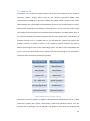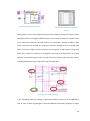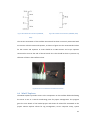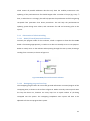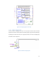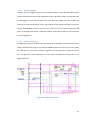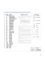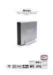
1
Instrumentation and Control Laboratory Facility Upgrade Murdoch University – School of Engineering and Energy A report submitted to the School of Engineering and Energy, Murdoch University in partial fulfillment of the requirements for the degree of Bachelor of Engineering Supervisor: Associate Professor Graeme Cole Daniel Lau (30499037) 11/15/2010 1 Acknowledgements Associate Professor Graeme Cole John Boulton Will Stirling 2 Abstract The Instrumentation and Control (IC) laboratory facility uses a Supervisory Control and Data Acquisition system to provide users with the flexibility in designing and implementation of control systems. A new panel is being built and setup due to the growing demand of the IC laboratory facility; the Labview server program must also be expanded to fulfil for this upgrade. Additionally the current Labview server program has several problems within the system and requires some improvement to help student users to use it effectively. The I/O Control board within the new panel provides the necessary connections between the server and the field, as well as controlling the power board. This I/O control board has been configured and will be prepared for the wiring into the patch panel. The patch panel which is connected to both the I/O control board and the power board provides the necessary connections and power to the instruments in the field. The power board is currently being constructed within this project and required a new and clearer wiring diagram to help with the construction of the power board. With the help of the new wiring diagram, the reduction of wiring mistakes and failures provided safety for both the constructor and future users. With the introduction of the new panel, a Profibus network has also been introduced to the IC laboratory facility. The Profibus network provides a demonstration of alternative industrial communication system. Contrast to the established system it has a faster transmission rate, less wiring and intrinsic safety. 3 Table of Contents 1 Introduction .................................................................................................................... 8 1.1 Background ............................................................................................................. 8 1.2 Scope of Report ...................................................................................................... 8 1.3 Objectives ............................................................................................................... 9 1.4 Related Work ........................................................................................................ 10 1.5 Assumptions, Constraints and Risks ..................................................................... 11 1.6 Definitions and Acronyms..................................................................................... 12 1.7 Structure of the Report......................................................................................... 12 2 The Instrumentation and Control Laboratory Facility .................................................. 14 2.1 Master I/O............................................................................................................. 15 2.2 Power Board ......................................................................................................... 16 2.3 I/O Control Board.................................................................................................. 17 2.4 Profibus System .................................................................................................... 17 3 Labview Program (Master I/O) ..................................................................................... 19 3.1 Activation Table.vi ................................................................................................ 19 3.2 Patchnames.txt Corruption................................................................................... 21 3.3 Read/Write Previous I/O Listings .......................................................................... 25 3.4 Setting up Loop 4 .................................................................................................. 25 3.5 Labview Conclusion .............................................................................................. 27 4 Power Board.................................................................................................................. 28 4.1 Wiring Diagram ..................................................................................................... 28 4.2 Components Changes ........................................................................................... 31 4.2.1 New Thyristors ........................................................................................... 31 4.2.2 New 24VDC Power Supplies ....................................................................... 33 4.2.3 Transformer 5 Primary Circuit Breaker Current Rating.............................. 33 4.3 Wiring Up the Power Board .................................................................................. 34 4.4 Power Board Conclusion ....................................................................................... 36 5 I/O Control Board .......................................................................................................... 37 5.1 6B System ............................................................................................................. 37 5.1.1 6B Series I/O Devices ................................................................................. 38 5.1.2 Setting Up and Testing ............................................................................... 41 5.2 Other Components ............................................................................................... 43 5.3 I/O Control Board Conclusion ............................................................................... 44 4 6 Profibus ......................................................................................................................... 45 6.1 Technical Review – Profibus DP and PA................................................................ 45 6.2 System Setup in IC laboratory facility ................................................................... 45 6.3 Termination .......................................................................................................... 46 6.4 WinCC Explorer ..................................................................................................... 47 6.5 Testing................................................................................................................... 48 6.6 Profibus System Conclusion .................................................................................. 49 7 Future Directions .......................................................................................................... 50 7.1 Revamping Labview server program .................................................................... 50 7.1.1 Recording Previous Usability Listings ......................................................... 50 7.1.2 Alternation of Labview Coding ................................................................... 51 7.2 I/O Control Board Wiring Diagram ....................................................................... 54 7.3 Patch Panel and Power Board .............................................................................. 54 7.4 6B Series Settings on Older Panels ....................................................................... 55 7.5 Proper Housing for the New PA Measuring Equipment ....................................... 55 8 Conclusion & Project Experiences................................................................................. 56 9 Bibliography .................................................................................................................. 57 10 Appendix ....................................................................................................................... 58 10.1 Academic Supervisor Endorsement ...................................................................... 58 10.2 Appendix A ............................................................................................................ 59 10.3 Appendix B ............................................................................................................ 60 10.4 Appendix C ............................................................................................................ 61 10.5 Appendix D............................................................................................................ 65 10.6 Appendix E ............................................................................................................ 66 5 Table of Figures Figure 1-IC laboratory facility front panel ............................................................................. 14 Figure 2-IC laboratory facility back panel .............................................................................. 14 Figure 3-Master I/O as part of the 2 networks...................................................................... 15 Figure 4-Old power board ..................................................................................................... 16 Figure 5-Patch panel power sockets...................................................................................... 16 Figure 6-Patch panel connectors ........................................................................................... 17 Figure 7-I/O control board..................................................................................................... 17 Figure 8-IO_Manager 4.6 interface ....................................................................................... 19 Figure 11-Activation Table interface ..................................................................................... 20 Figure 12-Activation Table connected to Activation Table.vi in loop system ....................... 21 Figure 13-Test point readings ................................................................................................ 22 Figure 14-Normal procedure corruption ............................................................................... 22 Figure 15-Jumbled sequence of combining data................................................................... 23 Figure 16-Murdoch Campus Adjusted Sequence .................................................................. 23 Figure 17-Corrupted Patchnames.txt .................................................................................... 24 Figure 18- Blank Array Initialisation Size ............................................................................... 24 Figure 19-Remapping warning indicator ............................................................................... 24 Figure 20-Path to Rubbish.txt ................................................................................................ 25 Figure 21-Path to Patchnames.txt ......................................................................................... 25 Figure 22-Activation Table Adjustment ................................................................................. 26 Figure 23-Activation Table True Address Column ................................................................. 26 Figure 24-Various COM port settings .................................................................................... 26 Figure 25-Maximum number of Addresses ........................................................................... 27 Figure 26-loop 4 configured patchnames.txt ........................................................................ 27 Figure 27-Single line diagram ................................................................................................ 28 Figure 28-Semi-improved wiring diagram ............................................................................. 29 Figure 29-Implementation of Isolation Switch ...................................................................... 29 Figure 30-Old Thyristor (PAC-15-C) ....................................................................................... 32 Figure 31-New Thyristor (PAC-16) ......................................................................................... 32 Figure 32-Control modes and wave form of the Thyristors (Shimaden)............................... 32 Figure 33-New 24VDC power supply ..................................................................................... 33 Figure 34-Old 24VDC power supply....................................................................................... 33 Figure 35-Transformer 5 Primary Circuit Breaker ................................................................. 34 Figure 36-Conductor Sizes ..................................................................................................... 35 Figure 37-Earth & Neutral Bars ............................................................................................. 35 Figure 38-Power box.............................................................................................................. 36 Figure 39-4 RS485 serial card ................................................................................................ 37 Figure 40-6BP16-1 Analog backplane (Devices, 1997) .......................................................... 39 Figure 41-Process Current Inputs (Devices, 1997) ................................................................ 39 Figure 43-6B50-1 Digital Board (Devices, 1997) .................................................................... 41 Figure 44-Interconnection wiring (Devices, 1997) ................................................................ 42 Figure 45-Other adjustments made to the I/O control board .............................................. 44 Figure 46-DP/PA coupler in a system (SIEMENS, Bus links, 2006) ....................................... 46 Figure 47-Profibus DP termination (SAMSON, 2007) ............................................................ 47 6 Figure 48-Profibus PA termination (SAMSON, 2007) ............................................................ 47 Figure 57-Current Termination of Profibus PA network ....................................................... 47 Figure 49-Level sensor in PVC container tube ....................................................................... 48 Figure 50-pressure sensor with resized fitting ...................................................................... 48 Figure 51-RS485/2 board functional indicator ...................................................................... 51 Figure 52-remapping progress state loop ............................................................................. 52 Figure 53-Profibus remapping state ...................................................................................... 52 Figure 54-COM port numbers ............................................................................................... 53 Figure 55-New patch panel location (back) ........................................................................... 55 Figure 56-New patch panel location (front) .......................................................................... 55 Figure 1-6BP16-1 (analog backplane) .................................................................................... 68 Figure 2-6B50-1 (digital board).............................................................................................. 68 Figure 5-Interdevice connection............................................................................................ 69 Figure 3-6BP16-1 (analog backplane) .................................................................................... 70 Figure 4- 6B50-1 (digital board)............................................................................................. 72 7 1 Introduction The Instrumentation and control (IC) laboratory facility on the Murdoch Campus has been undergoing constant upgrade, to provide student users with usability and to increased capability of the Instrumentation and control laboratory. This document will discuss the various topics with regards to the project, allowing readers to view the direction and improvements the project had made during the course of time. The document will also explain in detail the technical aspects of the project. The approach of the various problems/improvements, assumptions, reasoning and analysis of the results from the actions that had been taken on each area of the project, will hopefully give readers a clear understanding on how the project unfolded. 1.1 Scope of Report The report will encompass any improvements and knowledge attained as the project unfolded. The report will discuss the various objectives that were developed as the project progressed. The report covers four main areas: Labview programming; Power board; I/O control board and the Profibus System. There will be a technical review to help the reader get a better understanding of the various systems around the IC laboratory facility. The report also includes documentation on the possible future directions and future recommended directions for the various sections in the IC laboratory facility. 1.2 Background Prior to the start of the project, there were numerous bugs, problems and unwanted programming in the Labview Master I/O program. The program was also found to be troublesome to use and over-complex, hence it was desired for the program to be revamped, allowing future users to pick up on the program quickly and easily, if there was a need for the program to be worked upon. A new panel is being built up to meet the growing demand for the need of panels in the Instrumentation and control laboratory. The panel would consist of a power board, an IO 8 control board, two patch panels and an equipment rack. The power board which powers the I/O control board and the other higher powered devices in the IC laboratory facility had its components laid out in preparation for it to be wired. However the wiring diagrams did not have sufficient information for it to be recreated and the previous power board poorly labelled, preventing users from easily locating connections. The I/O control board was supposedly completed and commissioned, but was later found to have some major issues (wrong Digital I/O boards were placed into the panel and SSRs and I/O modules had not been placed nor configured for the panel). The PLC had just been installed and programmed into the network and had not been tested. 1.3 Objectives The project would help the IC laboratory facility move towards an ultimate goal of having a new panel up and running. The project was aimed towards the upgrade of the IC laboratory facility, with the addition of a PLC into the new panel which is being set up in the IC laboratory facility. Areas have been left open for upgrades and work to be done. The upgrade would include both hardware and software improvements to the IC laboratory facility, the following areas were to be worked upon: 1. Labview (Master I/O) – There is a need for the improvement and debugging of the Labview program (Master I/O), which needed to be corrected and improved upon. It was a desired aim for the Labview program to be revamped. Due to the lack of time and the due to the complexity of the Labview program, significant documentation for the Labview program was made in preparation for future users to be able to easily revamp the Master I/O program. 2. Power Board (Bottom Box) – There was a need to generate a new wiring diagram which would improve and replace the previous wiring diagrams, allowing users to easily understand and be able to set up the power board. This included gathering 9 and preparation of the correct documents for the new hardware and size/types of wires for the power board, following this, the wiring of the power board, in preparation for it to be wired into the patch panel. 3. I/O Control board (Upper Box) – Ensuring that the control board works includes the connectivity of the PLC and the 6B system. There was a need for the configuration of the 6B boards and I/O Modules, to allow connectivity with the Master IO server program. Furthermore the replacement of an incorrectly placed 6B board. The board should be configured and ready to be connected to the power board and the patch panel. Installation and tidying up of the various components on the I/O control board had to be made. 4. Profibus PLC – This would include the testing of the Profibus equipment which was new to the IC laboratory facility. The equipment was ordered and brought in specifically to be connected to the Profibus network. 5. WinCC – To ensure the connectivity of the PLC which is connected via the use of WinCC, and updating the software to suit the new location from where the software is being run from. 6. Documentation – This part included the IClab website (a chad webpage system) keeping the CHAD webpage up to date to provide easy access for different level users. Technical documents, software coding and diagrams will be available on the EngShared server, for future users to attain important current information and previous software or information prior to the work done in this project. Customised user guides will be made to help future users to configure or even reconstruct sections in the IC laboratory facility. 1.4 Related Work One major part of the project was the testing of the program and different components within the IC laboratory facility. Simple gadgets where made to accommodate the various 10 sensors which were Profibus networked, as these sensors were slightly different in physical size or had different attachments which did not allow for connectivity with the existing instruments in the IC laboratory facility. Another important aspect to the project was the planning and communication with various people involved with the project, in order for the project to flow smoothly. 1.5 Assumptions, Constraints and Risks Several assumptions were made before and during the progress of the project. These assumptions would help constrain the various factors involved in the process of upgrading the IC laboratory facility. The current Labview software was assumed to be sufficient for the desired upgrade for the IC laboratory facility. This was done so as to have the users of the IC laboratory facility be able to easily use or manipulate the functionality of the facility. The wiring of the power control board will be checked by John Boulton, and information on wiring standards were informed through him, with some guidance from the AS/NZS 3000:2007 Wiring rules. Risk of incorrect wiring may occur even after triple checking with the redrawn wiring diagram. It was also assumed that the previously components fixed onto the control board were the correct components, fixed and labelled appropriately as well. Another constraint was related to the time that the other people involved with this project had, in which the project may or may not have been able to progress. The constraint that areas such as the patch panel will not be able to be completed by the end of the project period, due to the time consuming process of which the panel had to be sent to an external contractor for it to be cut; hence the wires that lead towards the sockets will be incomplete. 11 1.6 Definitions and Acronyms .vi - Labview program 6B - 6B series (Analog Devices hardware) AS/NZS 3000, Australian /New Zealand wiring rules COM - serial port ECLB - Earth Current Leakage Breaker EEPROM - Electrically Erasable Programmable Read-Only Memory ESB-DO-## - Experimental station Side B-Digital Output-## I/O - Input or Output IC – Instrumentation and Control PLC - process logic controller PVC - Poly(vinyl chloride) (Plastic) RTD - Resistor Thermal Detector SCADA - Supervisory control and data acquisition SCR - Silicon-controlled rectifier SSR - Solid State Relay VAC - voltage alternating current VDC - voltage direct current Vrms - Voltage root mean squared FMEA – Failure mode and Effect Analysis 1.7 Structure of the Report The Instrumentation and control (IC) laboratory facility consists of various aspects from different fields of knowledge, including power, control and computer systems. Due to the numerous aspects within the project of upgrading the IC laboratory facility, the report will be broken up into four major components: The Labview Server program, Power board, Input /Output (IO) control board and the Profibus system. A small introduction on the IC laboratory facility will be provided before the four major sections, to give the reader a feel on how the IC laboratory facility runs as a whole. The four major sections will then start with a brief introduction and within each section documentation on the background and problems will be discussed. Following this discussion, a report on what was done and the reasoning behind these actions, then review(s) of results or overlooked issues and how 12 each of them was addressed. Technical reviews will be interlaced amongst the various sections of the report, to help readers understand the capabilities of the numerous different components in the IC lab facility without having to remember all the technical details at the start of the report. A conclusion will end each major section, to provide a small review on that section. This document as a whole will end with a discussion of the possible future directions of the Instrumentation and Control (IC) Laboratory. 13 2 The Instrumentation and Control Laboratory Facility The Instrumentation and control (IC) laboratory facility is a multi-purpose SCADA (supervisory control and data acquisition ) system which allows users to be able to create a control system with its various analog inputs/outputs and digital inputs/outputs (I/O). This allows users to design and implement various control systems designs and algorithms with the use of a client based Labview program. The IC lab has a number of connection panels wired to a master I/O server which in turn is connected via Ethernet cabling to client workstations. The panels allow for a variety of instruments to be used and with the use of analog/digital connections, readings and signals can be received or sent to the connected instruments, as shown in figures 1 and 2. The server is connected to the patch panels via an RS485 network based on Analog Devices 6B Series I/O modules and Solid State Relays to connect with higher powered devices. Also with the use of the WinCC program, the server is connected through RS232 to a PLC which in turn connects to the instrument on the Profibus network. From the Master I/O Server using the Lab View and Data Socket software, users on client workstations are able to control the panel I/Os. Figure 1-IC laboratory facility front panel Figure 2-IC laboratory facility back panel 14 2.1 Master I/O The Master I/O is a Labview program which acts as the server program for the whole IC laboratory facility, reading various I/Os via the national instruments RS485 serial communication (COM3-6) to 6B series modules and COM1 which is linked to the newly added Profibus PLC. The Profibus network Master I/O server also communicates to various experimental workstations via Ethernet, collecting data in arrays from the various loops and sending and receiving data to the experimental workstations. The Data Socket server is the interface between the Labview program and the client workstation.. The Master I/O program basically acts as a middle man for the two different systems, 6B system and Profibus network, as shown in figure 3. The respective network transfers the data to Master I/O through the use of their networking system. The data is then manipulated and read or sent to the Data Socket server, which holds the data waiting for the workstation (Computer Users around the IC laboratory facility). 6B system Profibus Workstations Workstations Data Socket Data Socket Master I/O Master I/O PC - DAQ card WinCC program Analog/Digital Card Profibus PLC Field Instruments Field Instruments Figure 3-Master I/O as part of the 2 networks The master I/O server program is capable of doing multiple configurations such as, setting preferences, getting port signals, Configuration of 6B series hardware and its core sub program the IO_Manager. The IO_Manager sub program, deals with the mapping and 15 transfer of data. Originally there were 4 main loops in the IO_Manager program, each handling 2 patch panels in the IC laboratory facility. One main loop had been disabled as there were only 6 patch panels usable in the IC laboratory facility, when it was transferred from Rockingham. Another new loop has been set up for the Profibus system and the disabled loop has been reactivated and configured to suit the settings in the Murdoch Campus IC laboratory facility. The I/O manager allows users to ensure readings and help debug problems in the IC laboratory facility. It also allows for the disabling of I/Os to cut down on loop time. 2.2 Power Board The power boards hold the various protections devices, power supplies, transformers and thyristors, as shown in figure 4. These power boards protect users and equipment from the various high voltages or currents that occur in various situations. The power supplies, transformers and thyristors provide the necessary voltages and functions for the I/O control board and the various equipments, which are easily connectable via the patch panel in the IC laboratory facility, as shown in figure 5. Figure 4-Old power board Figure 5-Patch panel power sockets 16 2.3 I/O Control Board The I/O control board (as shown in figure7) contains the 6B analog and digital isolation devices, which allow communication between the server and the various measuring devices located around the IC laboratory facility. The various analog and digital, read or write devices are connected to a patch panel, as shown in figure 6, allowing a flexible implementation of various forms of control systems. The I/O handles the 6B series devices, which are connected via RS-485 to the server which can then be configured to the users’ specifications, through the use of the 6BWIN software. With the use of the Labview program, these devices can be used for various purposes and can then be used with the Data Socket system to communicate with the various workstations in the IC laboratory facility. The I/O control board also provides some protection for the short circuits or over currents, through the use of the 6B series devices internal circuitry and various fuses which have been connected to the I/O analog ports. The I/O control board also holds various connections to the control for and supplying from the power board. Figure 6-Patch panel connectors Figure 7-I/O control board 2.4 Profibus System The new I/O control board also contains the PLC (as shown in figure 7) which has now been included in order to implement the Profibus system. This Profibus network provides for more efficient communication between the server and the various equipments in the field. 17 The Profibus system brings variety to the IC laboratory facility. Further instrument or communication as part of the Profibus system includes the PA system (intrinsic safety system), although not required. This system may increase in size in the future years, as not only is it easier to transfer and rewire, it is also faster. Further details on the functionality of the Profibus system will be discussed in the “Profibus” section of the report. 18 3 Labview Program (Master I/O) The Master I/O Labview program acts like a server for the whole IC laboratory facility, dealing with the activation, data manipulation and mapping of the I/Os in the IC laboratory facility. Prior to the start of the project, there were several bugs and improvements that needed to be made. The next few sections will discuss on the modifications and actions. 3.1 Creation of the module known as the Activation Table.vi Prior to the I/O Activation table.vi, the IO_Manager 4.6 program used a cumbersome method to activate and deactivate addresses. Using the old programming code (Add_remove_module.vi), users had to enter an address and hold down an activate or deactivate button (shown in the bottom right corner of figure 8) for long periods of time (3-20+ seconds) for the adjustment of each address. The old code was troublesome and had flaws in changing the previous address when another address was entered for activation or deactivation, shown in the bottom right corner of figure 8. Due to having the Activate and Deactivate button in each main loop of IO_Manager, users were forced to hold the button till the loop was running again. The old code also used multiple loops within loops, which made the wait time for each change even longer and also caused the a bug when changing previously selected address. Figure 8-IO_Manager 4.6 interface 19 Work on the bug when changing previously selected address was a significant problem. It was then decided to work that section prior to any other changes. However much of the code was overcomplicated, causing uncertainties of when the controls were detected to adjust the I/Os and would cause corruption in the Patchnames.txt file (this will be discussed in the “patchnames.txt” section). For the system to be a robust and efficient system which would still be able to both activate and deactivate the various I/Os for each loop in the IO_Manager, it was decided that the system to use a different method of selecting addresses for activation and deactivation. By having a table with a listing of addresses and an adjustable column which allows for the activation or deactivation of the addresses on each loop interface, changes can be made by typing in a “1” for activation and a “0” for deactivation quickly and efficiently, shown in figure 11. Figure 9-Activation Table interface As a result of the changes made to the interface, the activation table brought on a new coding, hence removing the issue of altering previous addresses. The activation table of each loop was then be attached to the Activation Table.vi, which reads the activation table, splits and adjusts the number of I/O that should be present in the system and corrects usability states accordingly, this new code is shown in figure 12. Activation Table.vi still used parts of the old coding for the activation and deactivation of I/Os, but adjusted to fit 20 the new table system and capable of selecting appropriate data to increase its robustness. Activation Table.vi handles all I/Os in each loop, splitting and manipulating data for the various required formats of other Vis in the IO_Manager. Compared to the old coding system (Add_remove_modules.vi), the Activation Table method is simple, easy to use and significantly improves the usability. The program was released for testing engineering student users (2nd and 3rd year) who have found the new method much more convenient and efficient. Figure 10-Activation Table connected to Activation Table.vi in loop system 3.2 Patchnames.txt Corruption The Patchnames.txt corruption was known prior to start of this project. Previous programmers were unable or did not have to solve this problem. Patchnames.txt allowed users to retain information across the session. In order to find out what was actually happening to the Patchnames.txt file, several test points were added to the program particularly within finishing.vi, this included picking up readings of different types of data and formats, as shown in figure 13. 21 Figure 11-Test point readings When the program was ran following the normal procedures, corruption of the usability data were found to be overflowing into the Timestamp data section, shown in Figure 14. One of the main causing issue was that there were missing I/O addresses in the patchnames.txt file, which lead to an unequal number of usability data. This issue was solved with the introduction of a new sub program known as the Activation Table.vi, as it continued to write data on I/O addresses, which were not found during the remapping procedure. Activation Table.vi kept the I/O addresses for the finishing.vi to use and to prevent usability data corruption in the Patchnames.txt file. Figure 12-Normal procedure corruption Unfortunately this was not the only corruption source. Reviewing the original patchnames.txt with the corrupted.txt file, the addresses were being altered and jumbled data all over the place. This was due to the wrong sequence of combining data in the 22 IO_Manager.vi, Data was being combined in the sequence of loop2, loop1, loop 3, loop4 (Figure 15). This jumbling of sequence might have been due the shifting of loops and addresses when the IC laboratory facility was brought from the Rockingham Campus to the Murdoch campus. Hence adjustments were made to suit the Murdoch Campus IC laboratory facility address and loop sequencing, to prevent further corruption of the Patchnames.txt file, this code is shown in Figure 16. Figure 13-Jumbled sequence of combining data Figure 14-Murdoch Campus Adjusted Sequence However, still there was more corruption was occurring. Data in the patchnames.txt file started loading Timestamp data in sections where I/O address data was being written, as shown in figure 17. This problem was due to the initialised size of the blank array created each time the finishing.vi starts. This array size should only include the total number of I/O addresses, and this does not include the Timestamp data, shown in figure 18. With the wrong number of I/O addresses, the starting point for the Timestamp data would be formatted accordingly. 23 Figure 15-Corrupted Patchnames.txt Figure 16- Blank Array Initialisation Size This new version of the Master I/O program was made available to the 2nd and 3rd year engineering students, who often used the IC laboratory facility. Intriguingly, corruptions occurred again. Looking at the patchnames.txt file, there were missing I/O addresses and incomplete usability data. Testing on operations of shutting down and starting up were done, and when the IO_Manager was shut down during the remapping phase (remapping incomplete), corruptions for the patchnames.txt file reoccurred. This problem was solved by reading a separate text file with fixed data and replacing the missing data in the patchnames.txt file each time IO_Manager would start up. However it was decided that doing so would prolong the already long waiting time of loading the IO_Manager and would be tackled in a different manner. It was decided to have a large indicator to be shown next to the “stop” button on the IO_Manager interface, to warn users not to stop the program while remapping was incomplete (shown in figure 19). Corruption has yet to occur since the placement of remapping indicator, since the released for testing by the 2nd and 3rd year 2010 engineering students. Figure 17-Remapping warning indicator 24 3.3 Read/Write Previous I/O Listings As previous programmers were unable to fix or even realise the corruption of patchnames.txt file, a temporary fix was used by sending data to rubbish.txt file (Figure 20). The temporary fix did not provide the desired aims of the original code. Patchnames.txt was still being read from for its “previous” usability settings and I/O listings for which I/O data to be displayed on IO_Manager. Patchnames.txt had to be replaced as the path for I/O listings to be written in when IO_Manager was shut down, in order to attain its originally designed purpose (Figure 21). Figure 18-Path to Rubbish.txt 3.4 Figure 19-Path to Patchnames.txt Setting up Loop 4 Prior to the IC laboratory facility being transferred from the Rockingham campus to the Murdoch Campus, there were four loops, but only 3 were used to run 6 of the 8 patch panels. Certain Coding for loop 4 was already set up for patch panels 7 & 8, but needed to be changed to suit the set up on the Murdoch campus. Since the reconfiguration of addresses, total number of I/Os and the new Activation Table.vi, adjustments had to be made to prevent corruption and correct readings from the 6B I/O boards. After the new 6B I/O boards were set up and configured, for panels 7 & 8 adjustments had to be made in the new coding Activation Table.vi. Specifically the number of I/Os had to be configured to fit the exact number of I/Os in the loop (Figure 22). This was done to prevent corruption of the Patchnames.txt file; adjustments had to be made to the loop 4 activation table as well, in the 2nd column (True address) of the activation table, which tells the program the corresponding address for which the activation is to be adjusted (Figure 23). The True address column had to be configured for the configuration of the usability of the I/Os, when setting up loop 4. 25 Figure 20-Activation Table Adjustment Figure 21-Activation Table True Address Column Configurations in the normal sequence loop were also made for setting up of loop 4, where COM ports had to be configured differently due to the change of COM port number, when the IC laboratory facility was brought shifted. The initialisation, Activation Table.vi, Read Write.vi and loop info.vi COM port constants had to be changed to fit the existing COM port 6, as shown in figure 24 below circled in red. The green circled constant in figure 24 shows the number that needs to be changed for the fitting of analog devices to be read and sent for the patchnames.txt file, this will have to be altered to the maximum number of analog addresses present in particular loop of IO_Manager. Figure 22-Various COM port settings In the remapping sequence, changes in Maximum number of I/Os had to be adjusted as well, in order to allow IO_Manager to read the addresses which were originally no higher 26 than 150. This maximum number of addresses is now configured to 200 to allow readings of loop 4 which have I/O addresses of 151 to 192, shown in figure 25. Figure 23-Maximum number of Addresses Figure 24-loop 4 configured patchnames.txt Lastly, the Patchnames.txt file had to be configured to allow the displaying of I/Os being read by IO_Manager. Addresses and configuration data had been added to the Patchnames.txt file, where 6B boards and modules had been configured and placed into the loop4 system, as shown in figure 26. 3.5 Labview Conclusion The Labview server program has now been debugged, solving previously known issues and improved in a few different areas. These improvements will provide greater usability of the Master I/O program, and reactivation of its broken hardware debugging software. The Labview program still has room for improvement but in particular it needs to be completely redesigned and the need for revamping. This is due to the continual small improvements and additions to the program have now made it very complicated and difficult to understand. More information in the documentation and ideas for the revamping of the Labview program, are contained in the “Future Direction” section. 27 4 Power Board The power board has been designed to power the I/O board in the box above the power board and sends power to power sockets to power equipment, such as pumps, heaters and measuring devices that need the high AC voltage. Components for the power board had already been bought, based on the previous boards and had to be assembled and wired in preparation for the powering of the panel. The power sockets have yet to be wired and commission due to the patch panel not being ready for the panel. 4.1 Wiring Diagram The original wiring diagram prior to the construction of the IC laboratory facility was a single line diagram. It had some information on the wiring diagram, shown in Figure 27. However, there was little information on how each component was to be connected, which made it very difficult for the uniquely wiring up of the power board, many assumptions would have to be made upon using the single line diagram. Figure 25-Single line diagram Prior to the start of this project, improvements were made to the wiring diagram. Providing a bit more information on how major components had to be wired up, as shown in Figure 28. However, not all the required information on how all components were to be wired was included in the diagram. 28 Figure 26-Semi-improved wiring diagram Much time was spent in improving the wiring diagram in the course of the project period. the wiring diagram was made for users to have enough information to set up the power board, shown in Appendix A. The main aim of the wiring diagram was not only to help with the production of the power board, but the safety and for future review and use. During the course of documenting the wiring diagram, certain important details on the power board and its connections were identified to be anyone who may have to construct the board or indentify possible issues. These important details are as listed below: 1. 1-9A &1-9B are multi-core wires that are used to connect the power supply board with the patch panel’s power connections. There will be an isolation switch between these wires and the actual power supply socket (Figure 29) Figure 27-Implementation of Isolation Switch 29 2. 24VDC drawn for the relay coils is taken from the control board’s 24VDC+ coming from T4+ (Power Supply 4). 3. There is a reduction to four 240VAC sockets for the new patch panels (2010-11-09) instead of the original six 240VAC sockets. 4. Thyristors A & B are running straight from the mains; They use the circuit breakers on the power board, as Thyristors used in the power board do not have over-current are not connected via the Earth Leakage Circuit Breaker (ELCB), this may be due to the sensitivity of ELCB, being able to detect tiny amounts of current changes in the Thyristors circuitry, which is likely to occur each time the Thyristors is set to a different voltage. 5. Thyristors A is controlled by the ESA-DO-04 and Thyristors B is controlled by ESB-DO04. 6. 110VAC power sockets are named “C/B1-4” on the patch panel and will use a yellow power socket cap. 240VAC Sockets will use a blue power socket cap and will be labelled “ESA-DO-06 to ESA-DO-12” or “ESB-DO-06 to ESB-DO-12”. 3-phase power supply sockets will use a red power socket cap. 7. Signal for the coils come from the SSR connections (DB-05A to DB-11A for panel A and DB-17A to DB-23A for panel B). 8. Required connections to the earth and neutral bars, have been listed on the right of the bar symbols. 9. Dotted line areas represent section that will be connected to outside of the power box. 10. Emergency stop buttons are connected before the mains enters the power box and are not indicated in the wiring diagram. 11. Labels 1-10A and 1-10B are numbered in accordance to the patch panel, where 1A and 1B are at the top of the patch panel and 10A and 10B are at the bottom of the patch panel. 30 These important notes have been placed in the wiring diagram’s legend to provide further details on the information that cannot be shown clearly on the wiring diagram, shown in Appendix B. The legend also includes a listing of components which can be crossreferenced to the power board layout diagram and short description on the component. 4.2 Component Changes Certain changes to the hardware components have been made as compared to the previous older set ups, due to components not being in production or questionable implementations. These changes in components have been discussed with Graeme Cole and John Boulton, before any implementations had been made on the actual power board. 4.2.1 New Thyristors One of the changes is the Thyristors, which are no longer in production. The old Thyristors in the previously set up power boards have basic features of zero voltage switching, adjustable power supply and current capacity of 20~100 Amperes, shown in figure 30. The new Thyristors have same features as the old one, convenient mode settings, zero voltage switching or phase angel control, soft start, slow rise and slow fall function, as shown in figure 31 below. 31 Figure 28-Old Thyristor (PAC-15-C) Figure 29-New Thyristor (PAC-16) 4.2.1.1 Technical Review – Control Modes Thyristors use different control modes producing different wave forms. Information on the different types of control modes are documented in figure 32. The main advantage of zerovoltage switching control which is currently used in the old control board set up is the lower cost due to the fewer Silicon-controlled rectifier (SCR) and having less noise as compared with the phase angle controlled Thyristors. In the case of the IC laboratory facility, zero-voltage switching control mode is being used and, as such on the new Thyristors when they are powered. Figure 30-Control modes and wave form of the Thyristors (Shimaden) 4.2.1.2 Technical Review – Soft start, slow rise/fall The Soft start function is to delay an output against changes in a control input signal whenever power is supplied. This produces an effect which helps to suppress rush current. The slow rise function mode increases the rise time of output in the event of an abrupt change of control input signal. For example when set data is changed during control 32 (Shimaden). The slow fall function slows the fall of the output in the event of sudden change to the input signal, similar to the slow rise function. Functions available in the new Thyristors, it may not be desirable to use them as it may cause confusion amongst experimental users, unless they are well aware of these functions. 4.2.2 New 24VDC Power Supplies New 24VDC power supplies were purchased as the previous 24VDC power supplies were no longer manufactured. Unfortunately there was no manual available on the old 24VDC power supplies. Based on the label on the old power supply, its function was 240VAC input and 5Amps 24VDC output, as shown in figure 34. The new 24VDC power supplies (Mean Well, SP-150-24) have an 85~264VAC input and 6.3A 24VDC output, as shown in figure 33. In addition the new power supply features protections for short circuit, overload, over voltage and over temperature. Figure 31-New 24VDC power supply Figure 32-Old 24VDC power supply 4.2.3 Transformer 5 Primary Circuit Breaker Current Rating The circuit breaker used on the primary side of transformer 5 on the old power board uses a 16A current rating. However a 10A current rating was documented for the transformer, as shown in Figure 35. The 16A current rating circuit breaker might be due to the high inrush current. However it was decided that a 10A current circuit breaker would be placed in the new power board. This would allow future users to see if the circuit breaker trips when the power to the power board is switched on, showing that the inrush current is 33 higher than 10A. As there is no documentation on why this was done, the change to a 16A circuit breaker in replacement of the originally designed 10A circuit breaker should be documented if the need for replacement arises. Figure 33-Transformer 5 Primary Circuit Breaker 4.3 Wiring Up the Power Board Prior to wiring the power board, the wiring diagram was reviewed in consultation with John Boulton, Technical Officer into the school. Information for wiring such as conductor size and Protective device ratings were also checked based on the AS/NZS 3000 (NHP, 2005). Based on these sources, wiring sizes were chosen for the power box, where conductor sizes from the main switch to the circuit breakers were sized at 2.5mm 2, conductor sizes from the protective devices (8-16Amps) to other components were 1.5mm2 and signal conductor sizes were 1mm2 (Figure 36). Most parts of the power board run at a no higher than 16Amps. Power drawn from the main switch board is less than what is actually available (25Amps). Hence wire sizes from the main switch to the protection devices can be adjusted to suit the load of no higher than 16Amps, with 9Amps to spare which can go to a sub power circuit if the need arises. 34 Figure 34-Conductor Sizes Figure 35-Earth & Neutral Bars Certain Neutral wires are in orange and light blue colours. These however are not in the standard of AS/NZS3000 and should be black in colour (Figure 37). This was due to cable sizes not being available, and would not have been able to be bought and shipped in time for the end of the project. Hence it was decided to use these colours as a temporary wire to give a clear indication of where the neutral wire will have to run, before the shipping of the new multi-core cables arrive. Apart from these wires the power board itself is complete. However the power board cannot be cleared for powering up as grounding for the box, emergency stop buttons, main switch and isolation of multi-core cable leading to the patch panel is not yet complete. These issues are to be resolved by John Boulton, as grounding of the box requires unique clamps to secure the earth lines, main switch and emergency stop buttons require drilling of the power box or cutting of thick metal, and isolation of multi-core cable is dependent on how the patch panels are to be made. More discussion on what needs to be done will be discussed in the “Future Direction” section. 35 Figure 36-Power box Multi-core cables have been used and labelled for the wires that are leading to the patch panel power sockets for clear indication of where they should go and to make the power box cleaner, to also allow future users make it easier to follow the wiring (Figure 38). Multiple checks on the wiring of the power board have been cross-referenced to the updated wiring diagram and previous power boards, in order to help prevent any event of failure due to wiring issues. As the patch panel could not be made in time before the end of the project period, cabling could only be done in preparation for the patch panel. Cables have been labelled and information on how they are to be wired has been stated in the legend. Further details on what needs to be done will be discussed in the “Future Direction” section. 4.4 Power Board Conclusion The new power board is currently near completion, with minor adjustments and wiring to the patch panel left to be done. The board can then be checked in conjunction with the new wiring diagrams, and can be connected to the mains for testing. The new component changes will hopefully provide more flexibility in new control systems. 36 5 I/O Control Board The I/O control board is set up to provide control: of the relay section for the power board as well as input and out signal connection to the patch panel. In the beginning, the I/O control board was assumed to have the correct components clearly assembled onto the board. However during the process of commissioning the I/O control board and configured it for the Labview program IO_Manager, certain components were found to be incorrectly placed and wired. Thus additional work had to be done to get the board ready for connected into the power board for running. 5.1 6B System The Analog Devices 6B product family consists of backplanes, digital boards and analog modules, which allow for direct communication between the server and the different I/Os in the field. The 6B system is used to deal with remote I/O, removing the need to use pointto-point wiring directly to the server computer. The 6B devices use a serial communication specifically RS-485 to communicate between 6B devices. In the IC laboratory facility, these communication lines are wired using cables, which are plugs into a RS485 serial card in the computer, shown in figure 39. Where the Labview program can use this RS485 serial card for communication to the I/Os and 6BWin software allows for easy configuration of the various 6B series I/O devices. Figure 37-4 RS485 serial card 37 5.1.1 6B Series I/O Devices The 6B series I/O devices are highly configurable as they contain internal circuitry, using microcontrollers and EEPROM to communicate with similar devices. Up to 255 I/O channels maybe included as a single RS-485 communication line. The 6B analog modules and digital boards use non-volatile memory to store configurations, such as addresses, calibrations and other parameters. The 6B analog and digital systems have isolation devices that protect the devices from over currents or short circuits. 5.1.1.1 Analog The 6B series analog field devices use two main components: the backplane and the analog module. The backplane acts as a rack for the analog modules and as a routing power and communications to all the modules, to other boards or the server. The analog backplane that is used in the IC laboratory facility is a 6BP16-1 backplane, shown in figure 40. It uses RS-485 to communicate with other 6B devices or the server, including a RS-485 repeater to allow distances of up to 4000ft for later boards. The 6BP16-1 Analog backplane also can houses up to 16 analog devices, for either input or output power (Devices, 1997). A shunt diode is also present on the backplane, providing polarity reversal protection to the backplane. For the prevention of any short circuit or failure of other modules, a fuse (F1, in figure 40) is present and can be replaced. The two LEDs (CR3 and CR2, in figure 40) are status indicators, providing information on data transmission, board and module status. The configuration jumper (W1, in figure 40), allows for configuration for the analog module’s parameters, like address, baud rate, checksum status and integration time. Both the 6B11 and 6B21 analog devices have an EEPROM which stores calibration constants as well as configuration information. Details on how to configure these 6B series devices is available in a user guide “Configurations for the Adding or Removal of 6B series devices”, available in Appendix E. 38 Figure 38-6BP16-1 Analog backplane (Devices, 1997) 5.1.1.1.1 6B11 Isolated, field configurable analog input The 6B11 module is an isolated field configurable analog device, which have been configured to 19.2K baud rate, to maximise information transmission speed. These analog inputs have also been configured to ±20mA with 60ms Integration time. The use of a microcontroller allows for module output signals to be converted into engineering units as requested by the controller. For protection of the controller from the field, there is isolation between the field and controller side of the module of 1500Vrms. The analog inputs requires a 50 Ω precision resistor which converts the 20mA current signal to a 1V signal which is readable by the 6B11, as shown in figure 41. The plug in resistor fits into the two pin socket between the module terminals and the screw termination block, shown in figure 40 above. Do note that as the module’s inputs are bipolar, a negative value may mean that the user has reversed the high and low inputs on the screw terminal (Devices, 1997). Figure 39-Process Current Inputs (Devices, 1997) 39 The I/O modules in the previous panels have an integration time of 50ms, which may not be as desirable due to possible interferences with the power line frequencies in Australia. These integration times will have to be altered as further discussed in the “Future Direction” section. 5.1.1.1.2 6B21 Isolated, field configurable analog output The 6B isolated configurable analog output devices have been configured to 0 to 20mA and 19.2k baud rate to maximise information transmission rate. The slew rates for these analog modules are set to immediate. The output range for these modules is selectable between 0 to 20mA and 4 to 20mA, with a digitally-controlled isolated current loop output to a resolution of 12bits. The 6B21 module provides output protection of 240Vrms and 1500Vrms protection for the controller (Devices, 1997). Additional protection is available from the current flow being read back by an on-board isolated voltage-to-frequency converter, whose frequency is proportional to the loop current (Devices, 1997). This frequency signal is read back to a microcontroller through an optical isolator, where the frequency signal is scaled and returned to the host computer (Devices, 1997). 5.1.1.2 Digital The 6B series digital system in the IC laboratory facility utilises two 6B50-1 boards per I/O cabinet (2 panels), which are connectable via a 50 pin ribbon cable to two 24 slotted SSR racks. One is for inputs and the other for outputs. Similar to the other analog devices used in the IC laboratory facility, the 6B50-1 digital board communicates using RS-485 to the next board or backplane in the network. Similarly the digital I/O boards use a configuration jumper (shown in figure 43), where if placed on pins A and B, configuration of the board is available and if placed on pins C and B, only parameters such as input range, data format and integration time are available for change. The 2 LEDS (CR1 and CR2) shown in figure 43, present on the board show the communication status, where CR 1 provides information on transmission and CR2 flashes with the on board clock. A fuse (F1 on figure 43) helps to 40 protect the board from damage caused by short circuits, and the shunt diode provides power reversal protection to the board (Devices, 1997). Figure 40-6B50-1 Digital Board (Devices, 1997) 5.1.2 Setting Up and Testing Details on configuration procedures are explained in the user guide. However notable results and undocumented issues will be discussed in this section. Upon configuration of the analog board, it was noticed that additional modules placed in non-configurable sections of the analog backplane produced interference with the configurable port. It will be advised in the user guide to only configure one module at a time with no other modules attached to the backplane during configuration. As the power board had not been ready for supplying power, an external power sources was used for the configuration of the 6B series devices. About 0.5Amps and 5Volts was sufficient to run a couple of analog modules and the digital board, however when more modules were added onto the board, status indicators on the digital boards started to act up. The reasons for the status indicators did not function as per normal, after multiple tests were done on the EEPROM, the microcontroller and playing around with the number of analog modules on the backplane, it was soon noticed that the power levels had dipped below 4.5Volts. After placing the desired number of modules, the power source with the 41 new setup required 6.1volts and 1.85Amps, which is close to the voltage limit of the analog modules of 6.5Volts (Devices, 1997). Power levels on the external power source had to suit the needs of the 6B I/O setup, but the power panel will supply 5volts with a larger current to compensate for the lower voltage. Interconnections between the various 6B series devices were wired prior to the start of the project. It was noticed that these connections were not implemented with the recommended setup. Instead the grounds were connected at the end, as there is only one shield to allow the connected devices to have a common reference point. As terminals 1 and 2 are referenced to the left ground terminal and terminals 3 and 4 are referenced to the right ground terminal, shown in figure 44 below, by commoning all the grounds transmission of data is possible. Figure 41-Interconnection wiring (Devices, 1997) The 6BWin program allowed for the configuration and testing of the analog and digital devices as such this program was used as a tool for basic commissioning tests. As these devices would be used by a higher level program, IO_Manager.vi, the Labview program was 42 setup and configured to allow the usage of the new 6B configured devices. Readings and current changes were shown in the process of testing and the 6B series devices. 5.2 Other Components Several other components have been added onto the I/O control board, in order to have the panel to ready for powering, and wiring connections to the patch panel. As shown at the grey terminals in Figure 45 below where analog terminal connection AA-1C to AB-12C, have been commoned. 16 fuses (0.1A) were placed in line for the analog I/O devices for protection (shown in Figure 45 as black fuse holders), down from the 32 fuses in the older panels. The reduction in numbers of fuses placed into the I/O board was due mainly to the reduction in the number of analog I/O modules and sockets in the new panels compared with the old. Most of the time no more than four of each type of analog input or outputs were been used in the past. Connections T1± and T2± have yet to be commoned. Connections to the power supplies T1 and T2 have been disconnection for configuration of the analog and digital devices (shown as blue terminal blocks with separators in figure 45). The external power supplies are still in place, as the patch panel is still not ready and the power box has not yet been grounded. Hence the power board is not ready to supply the necessary power to the I/O control board above. 43 Figure 42-Other adjustments made to the I/O control board 5.3 I/O Control Board Conclusion Adjustments to the I/O control board have brought the cabinet closer to the completion of the new panel. Configuration of the new 6B series analog and digital modules and boards has been made, including the connectivity to the Labview server program. The I/O control board is waiting for the patch panel which will be sent for construction with the help of John Boulton. When the patch panel arrives, the analog and digital I/Os can be connected to it, providing practical usage of the I/O control board. 44 6 Profibus The Profibus system is a new core network system within the IC laboratory facility. It provides increased transmission rates of about 50% from the previous 19.2K baud rate. The following sub sections will provide information on how the Profibus system has been configured and setup. It also introduces new technologies and connectivity into the facility. 6.1 Technical Review – Profibus DP and PA Profibus DP uses a distributed I/O transmission protocol as an open bus system, whereas Profibus PA is an extension of Profibus DP being compatible in terms of communication. The high powered Profibus DP provides high transmission rates of up to 12MBaud. A DP master system can be extended to explosive areas by using DP/PA converters, where PA runs at a lower baud rate of 31.25K, but is capable of intrinsic safety for electrical equipment (SIEMENS, Bus links, 2006). 6.2 System Setup in IC laboratory facility The current Profibus system in the IC laboratory facility consists of a PLC (2 I/O modules), Server (using WinCC), Clients (which are the workstations) and the instruments in the field connected to the PLC. The PLC has 2 I/O modules, SIMATIC NET communication processor (CP342-5) and 2 DP/PA Coupler (FDC 157-0) to communicate to the various sensors out in the field. The communication processor (CP342-5) is designed to attach the PLC to a Profibus Fieldbus system. It can act as a DP class 1 master or a slave (SIEMENS, SIMATIC NET, 2006). A class 1 master can communicate actively only with its configured slaves and can communicate passively with a class 2 master. Whereas a class 2 master is capable of communicating with class 1 masters, the class 1 masters’ slaves and its own slaves for diagnostic, configuration and parameter/data exchanging. The DP/PA coupler acts as a physical link between the Profibus DP and Profibus PA networks. It is possible to connect up to five FDC157-0 (DP/PA couplers), which may be configured differently. With the use of an active field distributor (AFD) the network is set 45 up for ring redundancy, and with the use of an active field splitter the net work is setup for coupler redundancy, shown in the figure46 (SIEMENS, Bus links, 2006). In the case of the IC laboratory facility, there is a standalone DP/PA coupler which daisy chains to the devices in the field. Figure 43-DP/PA coupler in a system (SIEMENS, Bus links, 2006) 6.3 Termination Termination for signal wires is important, in order to prevent signal reflections on the Profibus PA or DP cable. Wrong or missing cable terminations may result in transmission errors or even completely losing communication link. Termination for the two different Profibus cables requires different termination. The Profibus DP uses active termination whereas PA uses a passive termination. The Profibus DP termination requires a 5V source, two 390Ω resistors and a 220Ω resistor, connecting as shown in Figure 47 below. Termination on PA requires a 100Ω resistor and a 1μF capacitor connected in series at the end of the PA branch line, as shown in figure 48 below. 46 Figure 44-Profibus DP termination (SAMSON, Figure 45-Profibus PA termination (SAMSON, 2007) 2007) The current termination of the Profibus PA network has been incorrectly terminated with an incorrect valued resistor and capacito, as shown in figure 56. The recommended values for the resistor and capacitor in series should be a 100Ω resistor and a 1μF capacitor connected in series at the end of the PA branch line. This should be done to prevent any reflection of data in the Profibus PA line. Figure 46-Current Termination of Profibus PA network 6.4 WinCC Explorer The WinCC explorer provides access to the components on the Profibus field and allowing the server to act as a central coordinating point for project management. The program gives the user details of the loaded project and shows all related file associated to the project. WinCC explorer allows for tag management, server computer setup, system 47 configurations and many other utilities. WinCC explorer has to start up prior to the loading of the Labview server program, as the program has not been set up to be able to reload new readings from the WinCC program into the Labview program. The WinCC configuration location of the server had to be altered during this project, as the previous configuration and testing computer was not the main server computer. 6.5 Testing Prior to the start of the project, pressure levels of the new pressure sensors were shown to change in the IO_Manager when air was blown into the pressure sensor. However the new measuring equipment had yet to be tested out for experimental purposes. This simple containment structures were built to encase the measurement equipment. John Boulton, a technician was brought into help construct these simple modified add-ons for usage in the IC laboratory facility, shown in figures 49 and 50 below. Figure 47-Level sensor in PVC container Figure 48-pressure sensor with resized tube fitting The pressure sensor was fitted with tubing and a resized cap to fit onto a level tank in the IC laboratory facility. The Level sensor was encased in a PVC tube which was sealed on both ends with an opening on the top with a screw-on fitting for the level sensor. The PVC tube 48 was fitted with taps and fittings to use the cold water supply in the IC laboratory facility. With the new setup, the measuring devices were again tested to show additional levels of readings, on both workstations and from the server. However, these instruments would require calibration as the results from the testing of the equipment showed that the level sensor could not go below 30% and the pressure sensor was at -3% to the IC laboratory facility’s atmospheric pressure. 6.6 Profibus System Conclusion The Profibus System is ready to be used. However having plugs and socket will provide more practicality and convenience to student users. The Profibus PA instruments will also require better containers for the storage of liquids and pressured gas/liquids, for usage in control systems set up by the users in the IC laboratory facility. These instruments will also require some calibration before usage in a proper control system. 49 7 Future Directions The future directions of this project are important to the completion of the total upgrading of the IC laboratory facility, as there are many viable options and possible improvements to help the IC laboratory facility run at its full capacity. The following sections will cover several recommendations for future directions to be taken under serious consideration, with regards to the upgrade and development of the IC laboratory facility. 7.1 Revamping Labview server program The revamping of the Labview server program is still a major concern of the upgrading of the IC laboratory facility. Due to the prioritisation of getting the 4th panel up and running, the program has gained some minor upgrades and debugging, however a total review and revamping of the program is required. Block diagrams on the Labview program have been created to help future users quickly grasp the major ideas of how the Master I/O server program functions. The block diagrams are shown in the appendix C (4 pages) and will be available in the EngShared server. A VI hierarchy has been included in the appendix D and will be available in the EngShared server. This will help users locate the various sub programs and to understand the structure of the server program. A few thoughts into the revamping of the Labview server program will be discussed in the sub sections below. 7.1.1 Recording Previous Usability Listings Previously the usability listings used a basic method of gathering data and writing over all of the previous data. With the use of the activation table, data on usability has been made more robust. However it is not entirely failure proof. After much work on the master I/O program, it has been found to be very troublesome to adjust multiple parts of the master I/O program, to prevent corruption of the patchnames.txt file. As the system is being revamped, the user should look into a method which alters the usability column of the patchnames.txt file alone. The addresses, tag name, station number, I/O type and port number should never be over written in the first place. The user should create a system 50 which retains all possible addresses data but only have the usability overwritten. The updating of the patchnames.txt file should happen after a number of loops (eg. every ½ hour, or when there is a change); this will help prevent the patchnames.txt file from getting corrupted from premature shut down procedures. This will help the patchnames.txt updating system being more robust, and convenient for add and removing I/Os to the system. 7.1.2 Alternation of Labview Coding 7.1.2.1 RS485/2 board functional indicator Currently the program made for this indicator, which is suppose to show that the RS485 board is functioning appropriately, is useless as it does not actually serve its true purpose. Rather it merely turns on the indicator when passing through the start up state, drawing a reading from a constant, as shown in figure 51. Figure 49-RS485/2 board functional indicator 7.1.2.2 Remapping progress bars loop The remapping progress bars do not actually provide information on actual progress of the remapping state, as shown in the red box in figure 52. Rather it merely counts up each time the loop has been run, however not every loop has an equal number of I/O being remapped into the system. The remapping completion state system will have to be adjusted to fit the new progress bars system. 51 Figure 50-remapping progress state loop 7.1.2.3 Profibus remapping state Currently Profibus remapping state servers no real purpose, however when the WinCC program has not been started up before the Labview program, tags cannot be picked up by IO_Manager. This blank state will serve a purposeful location for code on remapping tags from WinCC, shown in figure 53. Figure 51-Profibus remapping state 52 7.1.2.4 Profibus logging Currently there no logging system for the Profibus network, unlike the other 6B network which has patchnames.txt file which logs data from the previous session. This will help with the debugging of new devices which will most likely be added onto the Profibus PA network, or when device failure occurs. The profibus system should preferably not use the existing PATCHNAMES.txt file to log the data, as this may cause confusion when the 6B loops are drawing information, unlike the Profibus system which does not read off these previous logged data. 7.1.2.5 COM port numbers The COM port constant numbers have not entirely been changed to fit the actual COM port being used within the program. For example COM6 used from the server is at times calling for COM port 5 as a constant, as shown in figure 54. The users will have to look into certain sub .vi programs to make alterations to fit the new true COM ports being used in the higher level loop. Figure 52-COM port numbers 53 7.2 I/O Control Board Wiring Diagram Even though it is assumed there will not be any changes to the I/O control board, having a better I/O control board diagram will be useful for the future, should the need arise. Currently the wiring diagrams for the I/O control board, is quite vague when trying to relate to the planned layout drawing. Documentation of how the labelling code has been made would help create some sense in the way the labelling has been done. The current labelling on the I/O control board does not provide any indication on how the system is to be wired to the patch panel. In addition, having five A3 pages of wiring diagram can be very troublesome to follow and hard to understand. 7.3 Patch Panel and Power Board The patch panel which has yet to be created is an important section to follow up after this project. John Boulton is the person to contact, as he will be sending the metal plates to be specifically punched to fit the power switches, sockets and I/O connection sockets. Using information on the power wiring diagram will help with the wiring and isolation of the power sockets and switches. Information on the I/O connection sockets will have to made based on the old wiring diagrams. The power board is awaiting grounding of the power and I/O control cabinets to be done by John Boulton, as he has the proper equipment and expertise. When black colour 2.5mm diameter cable becomes available, wiring of the neutrals for cables that are orange and light blue attached to the neutral bars, will have to be replaced with the specific black colour 2.5mm cables. The isolation of the power cables should be done before any connections from the live lines are to be connected to the power board’s main switch. The metal pole which connects the main switch breaker and the switch on the box door is being cut by John Boulton. When these things are completed, the power board should again be cross-referenced with the updated wiring diagram with a different set of eyes to check that everything is consistent and correct. 54 The new patch panels which will be created, will be placed in the locations highlighted in red in the figures 55 and 56 below. Notice that in figure 55, that the patch panel has been located behind the power and I/O control boards, unlike previous panels, this is to allow for more rack space for equipment. Figure 53-New patch panel location (back) Figure 54-New patch panel location (front) 7.4 6B Series Settings on Older Panels The 6B series modules and boards integration time settings on the old panels are all on 50hz (60ms), these should all be altered to 60hz (50ms) as discussed in the 6B series section previously. Configuration procedures will be available in a user guide provided in the EngShared folder in Timoshenko, also shown in Appendix E. 7.5 Proper Housing for the New PA Measuring Equipment As shown in the Profibus testing section, the modified add-ons only made as temporary testing housing equipment. The need for a more experimental friendly housing will be required to be made for these new PA measuring devices. The housing should most definitely have some sort of sight glass or a transparent panel, for viewing of the level of water in the tank. Furthermore, the pressure measurement devices should have some sort of tank and housing for the sensor to be placed on the equipment racks. 55 8 Conclusion & Project Experiences The project has run rather smoothly with certain predicted delays in the course of the project. The Master I/O Labview program has been configured to meet the needs of the new panel and there has been reduction of bugs in the system. However it still requires a major redesigning and remaking. The I/O control board is complete and configured, ready to be wired to the patch panel, after the two new panels (patch panels 7 & 8) will be available for configuration in the facility. With the knowledge learnt in this project and documented, future users will be able to set up new panels from scratch with the help of these documents. The CHAD website has been updated in several areas and documentation in .pdf and .tcw (TurboCAD) are readily available in the “downloads” section of the website. The documents acquired in the process of this thesis will be available on the EngShared server under “IC_facility_2010”, this will include various documents, such as drawings, references and software, a list in shown in Appendix F. This project has brought about numerous experiences in the different fields of; Instrumentation and control, Electrical power and industrial computer systems. Through constant communication with the various experts in the respective fields, the project has brought along much learning experiences. The project still holds great purpose in both the present and the future developments in IC laboratory facility. 56 9 Bibliography Devices (1997). 6B Series User manual. In A. Devices. (Technical Manual) (Available on Timoshenko "IC_Facility_2010") NHP. (december, 2005). NHP. Retrieved 9 November, 2010, from www.nhp.com: http://www.nhp.com.au/latest_news/Technical%20news/documents/TNL46.pdf SAMSON. (2007). Profibus PA. In SAMSON, Technical Information. (Technical Manual) (Available on Timoshenko "IC_Facility_2010") Shimaden. (n.d.). MPU-Based single phase power regulator (PAC16). Retrieved 2010 11, 9, from www.get-point.com: http://www.get-point.com/get-point-pdf/pac16(NEW).pdf SIEMENS. (2006). Bus links. In SIEMENS. (Technical Manual) (Available on Timoshenko "IC_Facility_2010") SIEMENS. (2006). SIMATIC NET. In SIEMENS, S7-CP for profibus. (Technical Manual) (Available on Timoshenko "IC_Facility_2010") 57 10 Appendix 10.1 Academic Supervisor Endorsement ENG460 Engineering Thesis Academic Supervisor endorsement performance I am satisfied with the progress of this thesis project and that the attached report is an accurate reflection of the work undertaken. Signed: Date: 58 10.2 Appendix A – Power Board Wiring Diagram (Available Electronically) 59 10.3 Appendix B – Power Board Wiring Diagram Legend (Available Electronically) 60 10.4 Appendix C – Master I/O Block Diagrams (Part 1-4) (Available Electronically) 61 62 63 64 10.5 Appendix D – Master I/O VI Hierachy (Available Electronically) 65 Daniel Lau USER GUIDE 2010 10.6 Appendix E Instrumentation and Control Laboratory Facility Upgrade Murdoch University – School of Engineering and Energy Daniel Lau 2010 66 Table of Contents 1 Installation & Configuration of 6B series devices ......................................................... 68 1.1 Important notes .................................................................................................... 68 1.2 Required Information/Software ........................................................................... 68 1.3 Assumed devices used .......................................................................................... 68 1.4 Procedures ............................................................................................................ 68 1.4.1 Analog devices ........................................................................................... 69 1.4.2 Digital Devices ............................................................................................ 72 2 LabView configuration .................................................................................................. 74 2.1 Important notes: ................................................................................................... 74 2.2 Required information ........................................................................................... 74 2.3 Procedures ............................................................................................................ 74 2.3.1 Activation table configuration ................................................................... 74 2.3.2 Configuration of “Normal” loop in IO_Manager ........................................ 75 2.3.3 Configuration in “Remapping” loop ........................................................... 75 3 Troubleshooting ............................................................................................................ 76 67 11 Installation & Configuration of 6B series devices 11.1 Important notes Information is available in the 6B series devices manual, can be found in the “IC_facility_2010” folder It is best to configure each 6B series devices, before connecting all of the devices as a network, as each device has to be configured separately. The 6B backplanes for the analog devices and the 6B Boards both require 5V and ~0.3mA NEVER go above 6.5V, this will burn the boards!! 11.2 Required Information/Software COM port number Largest address number 6B WIN software 11.3 Assumed devices used Analog backplane: 6BP16-1 Analog Input module: 6B11 50 Ω precision resistor (black blocks) Analog Output module: 6B21 Digital board: 6B50-1 11.4 Procedures This section will be split into three parts, one each for analog devices, digital board and inter-device connections. The connection used in the Murdoch Campus Instrumentation and Control Facility is a RS485 cable, the 2 wires that are needed for configuration and connectivity to the server computer is in blue and white. The blue wire will have to be connected to terminal 3 and the white wire to terminal 4 of the analog backplane or digital board, in the red circles as shown in figures 1 & 2 below. Figure 55-6BP16-1 (analog backplane) Figure 56-6B50-1 (digital board) 68 11.5 Inter-device connection 1. Implement one of the following connections between the devices; ensure that the GNDs of the boards are connected to each other, as they are not commoned within each board, as shown in figure 5. Ensure that output signals go to inputs terminals; board diagrams input and output terminals shown in figures 3 &4. Figure 57-Interdevice connection 2. Connect the Ethernet communication cable from the server computer. 3. Power the devices and ensure that there is sufficient power (5V) at the power terminals of the board closest to the Ethernet cable. 4. Run Sixb (6B-WIN) software 5. When the MAIN MENU will pop up; click COMMS and use 19200 Baud rate and ensure that the max addresses includes the address the device is in. Press OK/DONE. 6. Run a SEARCH to ensure that all connected devices are present. 7. Any other issues review the “Troubleshoot” section. 11.6 Analog devices The following procedures should be followed when configuring the analog devices: 1. Ensuring that the Ethernet cable has been connected between the backplane and the server computer (see 1.4 for connection information). 2. Take out the configuration jumper 3. Place the analog module that is to be configured in the far left terminal (next to the Configuration Jumper, shown in Figure 3) 4. Ensure that no other modules are on the board (this may cause bugs) 5. Power the analog backplane at GND and +5V, as shown in figure 3. 69 Figure 58-6BP16-1 (analog backplane) 6. Open the Sixb program (6B-WIN), this leads you to a screen for COM port selection, select the COM port that you are connecting the device(s) to, as shown below. 70 7. After clicking the COM port, you will be lead to a selection screen, which stores previously “searched” devices, as shown below. Select one of these devices and press OK. 8. The MAIN MENU will pop up. Click COMMS and use 9600 Baud rate (a new board will have a default Baud rate of 9600 and address of 00) and ensure that the max addresses includes the address the device is in. Press OK/DONE. 9. Back at the MAIN MENU click on SEARCH and select the appropriate device (there should only be one, if you followed the steps) to enter Device Configuration, or else you will automatically be brought to a Device Configuration, where you can change the Address, Baud Rate and Integration Period. Some warnings on the changes in addresses and baud rate will pop up. *Ensure that the addresses are unique and the baud rate is 19200, for integrating with the Master I/O Labview software. Clicking on DONE, will lead you to the MAIN MENU. 10. Unpowered and Repower the 6B series device to load the configuration into the module. Repeat these procedures (Step 1-8) if more modules are to be configured. 11. When all the devices are configured, turn off the power supply. 12. Re-install the Configuration jumper (W1, n figure 3) place all the modules into their respective terminals. 13. Install the 50 Ω precision resistors, at the 2-pin terminals (below the module terminals) for analog input devices, shown in figure 3. 14. Power the board and ensure that there is sufficient power (5V) at the power terminals of the board closest to the Ethernet cable. 71 11.7 Digital Devices The following procedures should be followed when configuring the analog devices: 1. 2. 3. 4. Connect the Ethernet cable to the digital board you are configuring as shown in section 1.4 Switch the configuration jumper to common pins C & B. Ensure that no other devices are connected to the board (this may cause bugs) Power the board at points GND and +5V, as shown in figure 4. Figure 59- 6B50-1 (digital board) 5. Open the Sixb program (6B-WIN), this leads you to a screen for COM port selection, select the COM port that you are connecting the device(s) to, as shown below. 72 6. After clicking the COM port, you will be lead to a selection screen, which stores previously “searched” devices, as shown in below. Select one of these devices and press OK . 7. The MAIN MENU will pop up; click COMMS and use 9600 Baud rate and ensure that the max addresses includes the address the device is in. Press OK/DONE. 8. Back at the MAIN MENU, click on SEARCH and select the appropriate device (there should only be one, if you followed the steps) to enter Device Configuration, or else you will automatically be brought to a Device Configuration, where you can change the Address, Baud Rate and Integration Period. Some warnings on the changes in addresses and baud rate will pop up. *Ensure that the addresses are unique and the baud rate is 19200, for integrating with the Master I/O Labview software. Clicking on DONE, will lead you to the MAIN MENU. 9. Unpowered and Repower the 6B series device to load the configuration into the module. Repeat these procedures (Step 1-8) if more modules are to be configured. 10. When all digital boards have been configure, remove power from the board. 11. Rre-install the configuration jumper to pins A & B, as shown in figure 4. 12. Attach the 50-pin ribbon cable which is connected to the 24 SSR rack. 13. Power the board and ensure that there is sufficient power (5V) at the power terminals of the board closest to the Ethernet cable. 73 12 LabView configuration 12.1 Important notes This section seeks to explain procedures required for the configuration of the Master I/O Labview program, whenever additional 6B analog or digital devices are added to the network. If the address being removed in not the largest address of its type (Eg. Removing analog output address 182, amongst analog outputs addresses 180-185), it would be advised not to be removed, as it will likely be removed in the future. These procedures are made for the configuration in Murdoch University Campus Instrumentation and Control Laboratory Facility in 2010-11-16 12.2 Required information Serial COM port number Highest address used in the COM port Maximum number of analog addresses List of address to be added or removed 12.3 Procedures The following procedures will guide the user through the necessary adjustments in the Labview server sub .vi program, IO_Manager. Each section will have a picture of the location of the amendment(s) required, some information on the configuration required and the steps that are taken for the adding or removal of I/Os. 12.3.1 Activation table configuration The list of addresses in the “True Address” Column and the address header column in the Activation Table for the loop being configured contains the added I/O address. For the 6B digital board, the digital address should be from ##.1 to ##.23 in the address columns. 74 12.3.2 Configuration of “Normal” loop in IO_Manager Configuration in “normal” loop in IO_Manager, configuration of selected COM ports have to be ensured to be correct and the maximum number of analog addresses chosen in the Activation table have to exactly be the same. The following configurations make reference to the image above: Boxes labelled “1” will have to be configured to the actual serial COM port number Boxes labelled “2” will have to be configured to the actual serial COM port number minus one (Eg. COM port 6, a constant of “5” would be used). Box labelled “3” will have to be adjusted to the exact number of maximum analog addresses chosen in the Activation table. 12.3.3 Configuration in “Remapping” loop Configuration of the Baud rate and Highest address number will have to be configured in altered. The baud rate which is used in the IC laboratory in the Murdoch Campus is 19200. The following configurations make reference to the image above: Box labelled “1” will have to be adjusted if the Baud rate is not 19200 Boxes labelled “2” will have to be adjusted to the highest possible address number 75 13 Troubleshooting Symptom Module or board does not respond to host. Possible Cause The RS-485/Ethernet cable may be loose or not connected properly. The external power supply is not attach or is not supplying power You are using an incorrect baud rate Module or board The module or board is is not operating damaged or malfunctioning properly. Vibration or loose connection Incorrect wiring Missing or broken wires Overheating Electrical noise High line resistance Yellow and Green LED on 6B series board/backplane continuously ON Possible Solution Check the cable connection and review chapter 1.4 Check the power supply and ensure that the right amount of voltage is coming in (no higher than 6.5V) Verify that the baud rate is the same for the module/ board and the host computer (default 9600) Check the EEPROM Software and the processor chip. Fix it! Or you are in big trouble! Cushion the source of vibration and tighten connections Review the respective sections Replace the wires Ambient temperature should be less than 60degC (unlikely the case, IC Lab Facility Murdoch Campus has air-conditioning duct running into the I/O Control Panels) Control electromagnetic interference through better cable shielding and planned ground connections Use larger cable size (within 22-14 AWG range) Test each board/backplane or each modules individually Malfunction of the board/backplane or one of the modules Not enough power supplied Check power terminals of to the board/backplane the board/backplane closest to the Ethernet cable connections from the server computer Green LED goes You may have blown fuse F1 Replace with little off fuse251.500, 5A (for 6BP161 back planes) Replace with little fuse 251.500, 1½A (for 6B50-1) 76 Symptom 6B21 analog output module responds to all commands, but readback indicates that no current following. When using search option in 6B-Win, software doesn’t recognise any devices TIMEOUT error occurs when using 6B-Win Possible Cause The current loop is open Possible Solution Check wiring. Some multispeed host Use 6B-WIN from the hard computers cannot access disk. 6B-WIN using diskette Memory-resident programs may interfere with communication with the 6B series devices Address or Baud rate have been altered and are not recognised by 6B-WIN Run 6B-WIN while other programs are not running (Eg. Master I/O) Power cycle the 6B devices and search for the devices under the appropriate baud rate 77