1
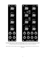
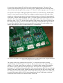
Oakley Sound Systems
5U Oakley Modular Series
VC-ADSR
Looping Envelope Generator
Building the ADSR Upgrade PCB issue 1
Builder’s Guide
V1.0.01
Tony Allgood B.Eng
Oakley Sound Systems
CARLISLE
United Kingdom
The left hand figure depicts the single width ADSR Upgrade module. This is designed to sit to the right of
our single width ADSR/VCA module. The right hand figure shows the double VC-ADSR module. This is
essentially a ADSR/VCA and an Upgrade module behind a common 2U wide panel.
Both modules contain the Oakley Upgrade PCB, but the VC-ADSR module also contains the main VCADSR PCB.
2
Introduction
This is the Project Builder's Guide for the issue 1 of the ADSR Upgrade and VC-ADSR 5U
modules from Oakley Sound.
This document contains a basic introduction to the Upgrade board, circuit description, a full
parts list for the components needed to populate the boards, and a list of the various
interconnections.
To build the full 2U VC-ADSR module you will need this document and the ADSR/VCA
Builder's Guide. The ADSR/VCA Builder's Guide can be found on the ADSR project
webpage:
http://www.oakleysound.com/adsr.htm
To download the latest User Manual, which contains an overview of the operation and all the
calibration procedures, please visit the main project webpage at:
http://www.oakleysound.com/vc-adsr.htm
For general information regarding where to get parts and suggested part numbers please see
our useful Parts Guide at the project webpage or http://www.oakleysound.com/parts.pdf.
For general information on how to build our modules, including circuit board population,
mounting front panel components and making up board interconnects please see our generic
Construction Guide at the project webpage or http://www.oakleysound.com/construct.pdf.
Nomenclature
VC-ADSR PCB: The PCB used in the Oakley ADSR/VCA module since January 2004.
ADSR Upgrade PCB: The PCB described in this document that allows the VC-ADSR PCB
to behave in a fully voltage controlled manner.
ADSR/VCA PCB: Our original envelope generator that used passive components as timing
controls. The PCB was superseded by the issue 1 VC-ADSR PCB in January 2004.
ADSR/VCA module: The module that, since January 2004, comprises of the VC-ADSR
PCB and, since August 2010, acts as a looping ADSR with a built in VCA on the output.
VC-ADSR module: The 2U fully voltage controllable looping ADSR module with integral
VCA.
ADSR Upgrade module: A 1U module that connects to an already constructed ADSR/VCA
module to allow for full voltage control of the attack, decay, sustain and release parameters.
3
The Oakley ADSR Upgrade Module
The issue 1 Upgrade PCB and handy Sock4 PCB behind a natural finish MOTM format Schaeffer panel.
The Upgrade board is designed to be used with the Oakley VC-ADSR boards. It enables the
four parameters, attack, decay, sustain and release, to be under full voltage control. The
Upgrade board connects with the VC-ADSR board via two four way ‘hidden’ interconnects.
The Upgrade board takes 1U of panel width and requires four socket inputs. It can be fitted
into either its own 1U panel, or be part of a 2U panel shared with the VC-ADSR board. For
the sake of clarity in this document we will refer to the 1U panel normally as the Upgrade
module and the 2U panel as the VC-ADSR module.
Please note in order to upgrade a ADSR/VCA module you need to have a VC-ADSR main
board. Very early versions of the Oakley ADSR/VCA module, prior to 2004, used passive
methods of controlling the attack, decay and release times and are not suitable for upgrading.
Your VC-ADSR board should be clearly marked as ‘VC-ADSR’ if you want to have the
ability to upgrade. Those marked as ‘ADSR/VCA’ and normally fitted with the green Omeg
Eco 16mm pots will not work.
The design requires plus and minus 15V supplies. The power supply should be adequately
regulated. The current consumption is around 25mA. Power is routed onto the PCB by a four
way 0.156” MTA156 type connector or the special five way Synthesizers.com MTA100
header. The four pins of the four way connector are +15V, ground, earth/panel ground, -15V.
The earth/panel connection allows you to connect the metal front panel to the power supply’s
ground without it sharing the modules’ ground line. More about this later. Provision is also
made for a second power connector to allow any connected VC-ADSR board to take its
power from the Upgrade board. Thus allowing both boards to be powered from just one main
power cable.
The PCB has four mounting holes for M3 bolts, one near each corner. These are not required
if you are using the three 16mm pot brackets. The board size is 143 mm (high) x 74 mm
(deep).
4
Circuit Description
The board simply consists of four identical attenuator and mixer circuits, along with various
headers to allow the signals on and off the board, and to provide connection to the power
supply.
Power is applied to the board through the PSU2, a 4-way MTA156 / Molex 0.156” connector,
or PWR2, a special five way MTA header. F1 and F2, small axial ferrite beads, provide some
high frequency resistance, and along with C13 and C14 prevent the board from being effected
by any noises on the power rails. They also help keep any unwanted noises going the other
way too.
Additional decoupling is also provided elsewhere on the board by eight other capacitors
shown above right of the power inlet circuitry. These capacitors keep the power supply clean
of noise, and provide a reservoir for the little bursts of current that the circuit takes in normal
operation.
Two grounds are provided, one for the circuit itself, and one for the earthing of the jack
sockets on the front panel.
The power supplies to each of the quad op-amp ICs are shown separately from the main
schematics to avoid cluttering the diagram.
The four inputs feature identical ‘reversible attenuator’ circuits. Let us consider the first
reversible attenuator. This takes its input from the line labelled ATTACK_CV and has its
output at ATTACK-OUT. The circuit is made up from four individual op-amps.
ATTACK_CV comes from pin 8 of the INPUTS header at the bottom of the board and is
connected to the signal lug of the ATTACK CV socket. R3 and R4 attenuate the signal
slightly to prevent any possible damage to the electronic circuits and also provide some
protection against static discharges. U1b (pins 5, 6 & 7) acts simply as a voltage buffer. This
is a circuit that merely ‘sniffs’ the voltage across R4 and creates a copy of that signal at its
output on pin 1. We are then free to take a bucket full of current from this output without
affecting the input at all. A bucket full of current must be defined here as anything less 15mA
or so... Hardly a bucket then, is it Tony??
U1a (pins 1,2 & 3) is a different circuit to the one around U2b. This is an amplifier with a
gain of -1. This means that its output is the opposite polarity to the input voltage. The input
voltage is sensed by R2, and the current flowing through R2, is matched by an equal current
flowing in the series combination of R1. The op-amp does this because it adheres to the
golden rules. (Actually, it can only try to adhere to these golden rules.) Now the golden rule
in question is that an op-amp with negative feedback must move its output so that its two
input pins are both the same voltage. The negative feedback is provided by the resistor R1. So
as the input signal tries to inject current into the op-amps inverting (-) pin via R2, the output
will move against this by taking that current away through R1.
5
So a positive input voltage at R2 will lead to the output going negative. The ratio of the
resistors will determine the gain of the inverting circuit. Making both the resistors the same
value will mean that the gain of the op-amp is -1. That is 5V at the input gives us -5V at pin 1
We now have two copies of the input signal. One, from U1b, is an exact copy, and the other,
from U1a, is an inverted version. These two voltages are placed across the two ends of the
control pot. As the pot wiper moves from one side to the other, it will tap off a proportion of
each signal. Consider what will happen with a +5V input signal across input resistor R4. This
will give +5V at the output of U1b and -5V at the output of U1a. The wiper of the pot can
thus move from +5V to -5V. In the middle position, both voltages take equal precedence and
the voltage at the wiper is zero. R17 loads the wiper voltage causing the linear pot to behave
in a non linear fashion. The pot becomes increasingly less sensitive near the middle of its
rotation thus making it easier to control small levels of modulation.
The two four way headers (A-D, S-R) and the additional power header (PSU1) on the Upgrade board that
connect to the adjacent VC-ADSR board.
The voltage at the wiper, and therefore across R17, is connected to another inverting
amplifier based around U1d (pins 12, 13 & 14). The op-amp’s gain is also minus one. So a
voltage of +5V at the wiper of the pot, will give -5V at the op-amp’s output. The amplifier
has another resistor connected to its input pin, R20. This resistor is very important to us
building the VC-ADSR and Upgrade modules. The current flowing in R20 will sum with that
flowing in the other input resistor. In other words this circuit will mix the wiper voltage with
the voltage present at the point labelled ATTACK-IN. This point goes back to one of the pins
on a four way header called A-D. The decay channel also uses the A-D header, whilst the
sustain and release channels use another header called S-R.
6
The headers are shown at the bottom right of the circuit diagram. You can see each one has
two inputs and two outputs. This is because the A-D and S-R headers serve two purposes.
One, they allow the Upgrade board’s output voltages to get to the VC-ADSR board. And two,
they allow for the ADSR’s pot settings to be sent to the Upgrade board. The Upgrade board
not only processes the input CVs but also adds them to the VC-ADSR board’s own settings.
Only then are the summed CVs are then passed back to the VC-ADSR core. This might seem
a little odd but it means that the VC-ADSR board does not need to have summing circuitry
included and thus the PCB can be physically smaller. The summing circuitry is only needed
with the full VC-ADSR module so it was not necessary to put it on the main VC-ADSR
board which is quite often used without external CV inputs.
As the output of the mixer is inverting, we need to invert it once again to get it the right way
up. U1c (pins 8, 9 &10) is configured as yet another inverting amplifier.
At the output of the final inverting stage is a small voltage limiting network based around a
resistor, R23, and a Schottky diode, D1. These are used to limit the maximum output swing to
positive values only. A Schottky diode is used because its resistance drops dramatically when
it has around -0.2V across it. A normal junction diode needs at least -0.6V before this
happens. When D1’s resistance drops it shunts any excess negative voltage to ground, thus
preventing the output voltage to drop below -0.2V or so. This negative clamping is done to
protect the 4052 analogue switch on the VC-ADSR board. Applying too much negative
current to the inputs of this chip will cause it misbehave or possibly die.
The voltage across the diode is fed to the header A-D. Here it will travel to the VC-ADSR
board to control the rise time of the VC-ADSR’s integrator.
The other three channels are identical in operation to the attack channel.
The suggested layout normalises the decay CV input to the attack CV when no jack is
inserted into the ATTACK CV socket. This requires 3 way header NORM to be fitted and a
jumper put across pins 2 and 3. If normalisation is not required the jumper should be fitted to
fit across pins 1 and 2.
7
Parts List
For general information regarding where to get parts and suggested part numbers please see
our useful Parts Guide at the project webpage or http://www.oakleysound.com/parts.pdf.
The components are grouped into values, the order of the component names is of no
particular consequence.
A quick note on European part descriptions. R is shorthand for ohm. K is shorthand for kiloohm. R is shorthand for ohm. So 22R is 22 ohm, 1K5 is 1,500 ohms or 1.5 kilohms. For
capacitors: 1uF = one microfarad = 1000nF = one thousand nanofarad.
To prevent loss of the small ‘.’ as the decimal point, a convention of inserting the unit in its
place is used. eg. 4R7 is a 4.7 ohm, 4K7 is a 4700 ohm resistor, 6n8 is a 6.8 nF capacitor.
This board may also be used with our older simpler front panel design. However, there are
small differences to the board components used for each option.
Resistors
All 5% carbon 1/4W or better.
4K7
8K2
10K
33K
100K
470K
R23, R30, R37, R44
R17, R24, R31, R38
R3, R7, R11, R16
R1, R2, R9, R10, R5, R6, R13, R14
R21, R22, R28, R29, R35, R36, R42, R43
R18, R19, R20, R25, R26, R27
R32, R33, R34, R39, R40, R41
R4, R8, R12, R15
Capacitors
33pF 2.5mm ceramic
100nF 63V axial ceramic
2u2, 63V electrolytic
C9, C10, C11, C12
C1, C2, C3, C4, C5, C6, C7, C8
C13, C14
Discrete Semiconductors
BAT-42 Schottky diode
D1, D2, D3, D4
Integrated Circuits
TL074 quad bi-fet op-amp
U1, U2, U3, U4
8
Pots
All pots 16mm Alpha or equivalent.
47K or 50K linear
ATTACK, DECAY, SUSTAIN, RELEASE
Alpha pot brackets
3 off
Miscellaneous
Leaded axial ferrite beads
L1, L2
MTA156 4 way header
MTA100 6-way header
PSU1, PSU2 – Oakley/MOTM power supply
PWR1, PWR2 – Synthesizers.com power supply
3-way 0.1” pin header
0.1” jumper
NORM
NORM
– for setting normalisation mode
– for setting normalisation mode
Molex/MTA 0.1” header 8-way
Molex/MTA 0.1” housing 8-way
Molex/MTA 0.1” header 4-way
Molex/MTA 0.1” housing 4-way
INPUTS
INPUTS
A-D, S-R
4 off
– for connecting to sockets
– for connecting to sockets
– to connect to VC-ADSR board
– to make VC-ADSR interconnects
Switchcraft 112APC 1/4” sockets
Four off mounted either on the Sock4 board or on panel
Four knobs
Around 2m of insulated multistrand hook up wire. Suitable power lead.
Additional components required if using optional Sock4 board
Molex/MTA 0.1” header 8-way
Molex/MTA 0.1” housing 8-way
I/O
I/O
112APC Switchcraft 1/4” socket
SK1, SK2, SK3, SK4
Two wire links are to be fitted to L1 and L2 on the Sock4 PCB.
If using Molex KK you'll also need at least 16 crimp terminals.
Suitable lengths of wire to make up the single 100mm interconnect and two cable ties.
9
Other Notes
The normalisation header is a 3 pin 0.1” header and associating jumper. In this jumper position
normalisation is activated.
The normalisation jumper is either fitted on the first two pins or the last. It simply sets
whether the Attack CV socket is normalised to the Decay CV input if no jack plug is inserted
into the Attack CV socket.
Pin 1 is the square pad on the NORM header When pin 1 and pin 2 are connected the Attack
CV input socket is not normalised.
If you do not need this feature to be selectable simply use a wire link to permanently set your
choice.
Note that the suggested front panel layout uses a small arrow between the attack and decay
sockets to indicate the normalisation. Thus this front panel layout expect pins 2 and 3 to be
linked or jumpered.
10
Connections
Power connections – MOTM and Oakley
The PSU1 and PSU2 power sockets are 0.156” Molex/MTA 4-way header. Friction lock
types are recommended. This system is compatible with MOTM systems.
Power
Pin number
+15V
Module GND
Earth/PAN
-15V
1
2
3
4
Pin 1 on the INPUTS header has been provided to allow the ground tags of the jack sockets to
be connected to the powers supply ground without using the module’s 0V supply. Earth loops
cannot occur through patch leads this way, although screening is maintained. Of course, this
can only work if all your modules follow this principle.
Power connections – Synthesizers.com
The PWR1 and PWR2 power sockets are to be fitted if you are using the module with a
Synthesizers.com system. In this case you should not fit the PSU header. The PWR header is
a six way 0.1” MTA, but with the pin that is in location 2 removed. In this way location 3 is
actually pin 2 on my schematic, location 4 is actually pin 5 and so on.
Power
Location number
Schematic Pin number
+15V
Missing Pin
+5V
Module GND
-15V
Not connected
1
2
3
4
5
6
1
2
3
4
5
+5V is not used on this module, so location 3 (pin 2) is not actually connected to anything on
the PCB.
If fitting the PWR header, you will also need to link out pins 2 and 3 of PSU1. This connects
the panel ground with the module ground. Simply solder a solid wire hoop made from a
resistor lead clipping to join the middle two pads of PSU together.
11
Power connections – MOTM/Oakley and Synthesizers.com
The Upgrade module has been fitted with two sets of power headers. This is so the Upgrade
board can power the connected VC-ADSR board. Thus only one power lead is required to
feed both boards.
PSU1 and PWR1 are laid out to be directly in line with the power headers on the VC-ADSR
board. If you are building the full 2u version of the VC-ADSR module, then you can use
these headers to simply connect the two boards together with a short 4-way jumper lead. You
can make this jumper lead so that each end is terminated in a MTA housing, or you can solder
the power lead directly into the ADSR board and then use a MTA header/housing on the
other end that plugs into the Upgrade board.
Building the Upgrade or VC-ADSR module using the Sock4 board
This is the simplest way of connecting all the sockets to the main board. The Sock4 board
should be populated in the way described in our construction guide found on the project
webpage. There is only one eight way header and it is to be fitted to the bottom side of the
board. Don't forget to solder in the wire links L1 and L2.
You need to make up only one eight way interconnect. It should be made so that it is 100mm
long.
The Sock4 makes a very neat job of wiring up the four sockets.
12
Hand wiring the sockets
If you have bought Switchcraft 112A sockets you will see that they have three connections.
One is the earth or ground tag. One is the signal tag which will be connected to the tip of the
jack plug when it is inserted. The third tag is the normalised tag, or NC (normally closed) tag.
The NC tag is internally connected to the signal tag when a jack is not connected. This
connection is automatically broken when you insert a jack.
Once fitted to the front panel the ground tags of each socket can be all connected together
with solid wire. I use 0.91mm diameter tinned copper wire for this job. It is nice and stiff, so
retains its shape. A single piece of insulated wire can then be used to connect those connected
earth tags to pin 1 of I/O. Pin 1 is the square solder pad.
All the other connections are connected to the signal lugs of the sockets. The table below
shows the connections you need to make:
Pin
Pad name
Socket Connection
Lug Type
Pin 1
Pin 2
Pin 3
Pin 4
Pin 5
Pin 6
Pin 7
Pin 8
PANEL_GND
RELEASE_CV
GROUND
DECAY_CV
GROUND
SUSTAIN_CV
ATTACK_NC
ATTACK_CV
Connect to all sockets
Connect to RELEASE CV
Connect to DECAY CV
Connect to DECAY CV
Connect to SUSTAIN & RELEASE CV
Connect to SUSTAIN CV
Connect to ATTACK CV
Connect to ATTACK CV
Earth lugs
Signal lug
NC lug
Signal lug
NC lugs
Signal lug
NC lug
Signal lug
Board to Board Interconnects
Make up two sets of four way interconnects. Each one will be terminated in either a Molex or
MTA 0.1” housing. Make sure if you have used Molex headers on your PCBs that you use
Molex housings. Likewise make sure that MTA headers will be mating with MTA housings.
Select the length of each wire in the interconnect so that they will reach from the Upgrade
PCB to the VC-ADSR PCB. If you are making the 1U ADSR Upgrade module and have your
ADSR/VCA module on a separate front panel I would suggest making the leads long enough
so you can extract either module from your modular case without the leads getting stretched.
13
Final Comments
If you have any problems, an excellent source of support is the Oakley Sound Forum at
Muffwiggler.com. Paul Darlow and I are on this group, as well as many other users and
builders of Oakley modules.
If you can't get your project to work, then Oakley Sound Systems are able to offer a 'get you
working' service. If you wish to take up this service please e-mail me, Tony Allgood, at my
contact e-mail address found on the website. I can service either fully populated PCBs or
whole modules. You will be charged for all postage costs, any parts used and my time at
25GBP per hour. Most faults can be found and fixed within one hour, and I normally return
modules within a week. The minimum charge is 25GBP plus return postage costs.
If you have a comment about this builder's guide, or have a found a mistake in it, then please
do let me know. But please do not contact me or Paul Darlow directly with questions about
sourcing components or general fault finding. Honestly, we would love to help but we do not
have the time to help everyone individually by e-mail.
Last but not least, can I say a big thank you to all of you who helped and inspired me. Thanks
especially to all those nice people on the Synth-diy and Analogue Heaven mailing lists and
those at Muffwiggler.com.
Tony Allgood at Oakley Sound
Cumbria, UK
© November 2010
No part of this document may be copied by whatever means without my permission.
14