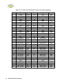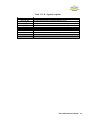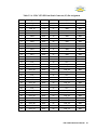
1
PXI-C1553
Hardware Manual
1/2/4 Stream MIL-STD-1553 Test and Simulation Module
for cPCI/PXI
September 2011
V01.00 Rev. D
3703 N. 200th Street,
Omaha, NE 68022
Tel: 866.246.1553
402.763.9644
Fax: 402.763.9645
aviftech.com
[email protected]
PXI-C1553
Hardware Manual
1/2/4 Stream MIL-STD-1553 Test and Simulation Module for cPCI/PXI
V01.00 Rev. D
September 2011
Avionics Interface Technologies
Omaha Headquarters
3703 N. 200th Street
Omaha, NE 68022
Tel: 866.246.1553
402.763.9644
Fax: 402.763.9645
Eastern Sales Office
34 Country Road
East Hampstead, NH 03826
Tel: 603.378.0957
Design & Production Center
2689 Commons Boulevard
Suite 201
Beavercreek, OH 45431
Tel: 937.427.1820
Fax: 937.427.1281 ext. 202
Western Territory Office
9221 E. Baseline Road
Suite A-109, #432
Mesa, AZ 85212
Tel: 480.354.0142
Notice: The information provided in this document is believed to be accurate. No
responsibility is assumed by AIT for its use. No license or rights are granted by implication in
connection therewith. Specifications are subject to change without notice.
© 2011 AIT
Table of Contents
....................................................................................................1
Section 1 INTRODUCTION
1.1 General .................................................................................................................... 1
1.2 How This Manual
....................................................................................................................
4
is Organized
1.3 Applicable....................................................................................................................
5
Documents
1.3.1 Industry Documents
...................................................................................................... 5
1.3.2 Product Specific
......................................................................................................
Documents
5
Section 2 STRUCTURE ....................................................................................................6
OF THE PXI-C1553 MODULE
....................................................................................................8
Section 3 INSTALLATION
3.1 Installing the
....................................................................................................................
8
PXI-C1553 Module
3.1.1 Installation Instructions
...................................................................................................... 8
3.1.2 Board Connectors
...................................................................................................... 8
3.2 Connections
....................................................................................................................
9
to the I/O Signals
3.2.1 Connection to the
......................................................................................................
MIL-STD-1553 Interface
9
3.2.1.1 Direct
..................................................................................................................
Coupling
10
3.2.1.2 Transformer
..................................................................................................................
Coupling
11
3.2.1.3 Direct
..................................................................................................................
to Device (Network) Coupling
13
3.2.2 PXI-C1553 Breakout
......................................................................................................
Cables
14
3.2.3 PXI-C1553 Front
......................................................................................................
Panel Connector (J3)
17
3.2.4 PXI-C1553-EF......................................................................................................
Front Panel Connector (J3)
20
3.2.5 PXI-C1553-EF......................................................................................................
Rear I/O Connectory (J4)
22
3.2.6 PXI XJ4 Connector
...................................................................................................... 25
3.2.7 IRIG Connections
...................................................................................................... 25
3.2.8 Discrete Connections
...................................................................................................... 25
Section 4 TECHNICAL ....................................................................................................27
DATA
PXI-C1553 Hardware Manual
II
Section 5 NOTES
....................................................................................................30
5.1 Acronyms....................................................................................................................
30
and Abbreviations
Section 6 APPENDIX A....................................................................................................32
III
PXI-C1553 Hardware Manual
1
INTRODUCTION
1.1
General
Document History
Version
Date
V01.00 Rev. A October 2010
Author
Description
Andy Kragick/Melissa
Created document
Amarawardana
V01.00 Rev. B
December
2010
Melissa
Amarawardana
Format revisions
V01.00 Rev. C
March 2011
Melissa
Amarawardana
Updated connector cable specifications,
Connecting the AIT Module to the Bus
V01.00 Rev. D
September
2011
Drew Dingman/Bill
Fleissner
Updated connector cable specifications
This document comprises the Hardware User's Manual for the PXI-C1553 hardware module
which is a member of AIT's family of advanced MIL-STD-1553 test and simulation modules.
This document covers the hardware installation, the board connections, a general description
of the hardware architecture, and specific electrical and physical technical data of the module.
For programming information, refer to the appropriate reference documents listed in the
Applicable Documents section of this manual.
The PXI-C1553 modules are capable of operations in both 3.3V PCI and PCI-X systems.
The modules can be used to simulate, monitor, and inject protocol errors in MIL-STD1553A/B systems and can provide up to 4 MIL-STD-1553 Dual Redundant interfaces. The
Full Function variant of the module is capable of simultaneously supporting the operations of a
Bus Controller (BC), Bus Monitor (BM), and up to 31 Remote Terminals (RT). The Single
Function variant of the module is capable of supporting either BC operations, or BM and
Monitor only RT operations, or up to 31 RT simulation operations. The Simulator Only
variant of the module is capable of simultaneously supporting BC operations, up to 31 RT
simulations, and up to 31 RT monitor only operations.
Both Transformer and Direct MIL-STD-1553 bus coupling modes are supported.
Additionally, an extended function variant of the module (PXI-C1553-EF) provides
additional functions that support software programmable MIL-STD-1553 bus coupling
(Transformer, Direct, Network, or Isolated) and software programmable output voltages.
The modules provide an onboard IRIG B Time Decoder/Encoder in support of time
synchronization with external equipment. Each module may be configured to synchronize its
internal clock to an input IRIG B time signal. Additionally, the module may also be configured
as an IRIG B time source capable of providing a reference time signal.
The PXI-C1553 module provide 10 programmable (as input or output) discretes. Each
PXI-C1553 Hardware Manual
1
discrete is capable of up to 30 V operations with an external power supply.
2
PXI-C1553 Hardware Manual
Table 1.1 - PXI-C1553 Variants
Part Number
Description
PXI-C1553-1
PXI-C1553-2
PXI-C1553-4
1, 2 and 4 channel full function interfaces for PXI
Simultaneous BC, 31 RTs and BM operations
IRIG-B Input/Output, 10 programmable discretes, PXI backplane
triggers and timing synchronization
PXI-C1553M-1
PXI-C1553M-2
PXI-C1553M-4
1, 2 and 4 channel single function interfaces for PXI
BC or 31 RTs or BM and 31 RT monitor only operations
IRIG-B Input/Output, 10 programmable discretes, PXI backplane
triggers and timing synchronization
PXI-C1553S-1
PXI-C1553S-2
PXI-C1553S-3
1, 2 and 4 channel simulate only interfaces for PXI
BC or 31 RTs and 31 RT monitor only operations
IRIG-B Input/Output, 10 programmable discretes, PXI backplane
triggers and timing synchronization
PXI-C1553-EF-1
PXI-C1553-EF -2
PXI-C1553-EF -4
1, 2 and 4 channel extended full function interfaces for PXI
Simultaneous BC, 31 RTs and BM operations
Programmable bus coupling/output voltage
IRIG-B Input/Output, 10 programmable discretes, PXI backplane
triggers and timing synchronization
PXI-C1553M-EF-1
PXI-C1553M-EF-2
PXI-C1553M-EF-4
1, 2 and 4 channel single function interfaces for PXI
BC or 31 RTs or BM and 31 RT monitor only operations
Programmable bus coupling/output voltage
IRIG-B Input/Output, 10 programmable discretes, PXI backplane
triggers and timing synchronization
PXI-C1553S-EF -1
PXI-C1553S-EF -2
PXI-C1553S-EF -3
1, 2 and 4 channel simulate only interfaces for PXI
BC or 31 RTs and 31 RT monitor only operations
Programmable bus coupling/output voltage
IRIG-B Input/Output, 10 programmable discretes, PXI backplane
triggers and timing synchronization
PXI-C1553 Hardware Manual
3
1.2
How This Manual is Organized
This manual is comprised of the following sections:
Section 1, INTRODUCTION, contains an overview of this manual.
Section 2, STRUCTURE OF THE PXI-C1553, describes the physical hardware
interfaces on the PXI-C1553 using a block diagram and a description of each
main component.
Section 3, INSTALLATION, describes the steps required to install the PXI-C1553
device and to connect the device to other external interfaces, including the
MIL-STD-1553 databus, IRIG-B, and discretes.
Section 4, TECHNICAL DATA, describes the technical specification of the PXIC1553.
Section 5, NOTES, contains a list of acronyms and abbreviations used in this manual.
4
PXI-C1553 Hardware Manual
1.3
Applicable Documents
The following documents shall be considered to be a part of this document to the extent that
they are referenced herein. In the event of conflict between the documents referenced and the
contents of this document, the contents of this document shall have precedence.
1.3.1
Industry Documents
MIL-STD-1553B, Department of Defense Interface Standard for Digital Time
Division Command/Response Multiplex Data Bus, Notice 1-4, January 1996
MIL-STD-1760, 1 August 2003, Department of Defense Interface Standard for
Aircraft/Store Electrical Interconnection System
PICMG 2.0 R3.0 CompactPCI Specification
PXI Hardware Specification, Revision 2.2, PXI Systems Alliance
PXI Hardware Specification, Revision 2.2 ECN 1, PXI Systems Alliance
PCI Local Bus Specification, R2.3 &3.0
PCI-to-PCI Bridge Architecture Specification, Revision 1.1
1.3.2
Product Specific Documents
AIT MIL-STD-1553 Getting Started Manual, provides detailed instructions to
assist first time users of AIT MIL-STD-1553 interface modules with software
installation, hardware setup, and starting a sample project.
AIT MIL-STD-1553 Object Wrapper Library Reference Manual, provides a
detailed description of the high level object oriented programming interface between
host application programs and the PXI-C1553.
PXI-C1553 Hardware Manual
5
2
STRUCTURE OF THE PXI-C1553 MODULE
The structure of the PXI-C1553 module is shown in Figure 2 below.
Figure 2 - Structure of the PXI-C1553
6
PXI-C1553 Hardware Manual
The primary components of the PXI-C1553 are:
PCI to PCI Bridge
This bridge allows multiple devices (namely the PMC1553 and PXI Trigger/IO
controller) on the on-card PCI bus. This bus runs at 33.333 MHz, whereas the
CompactPCI backplane may run at 66 MHz or 33 MHz.
MIL-STD-1553 Core/PowerPC FPGA
The MIL-STD-1553 Core and PowerPC is implemented in a Xilinx Virtex 4. The
PowerPC operates at 250MHz and is capable of hosting time critical user application
functions. The MIL-STD-1553 Core supports simultaneous Bus Controller, Bus
Monitor and Remote Terminal (up to 31) functions on each of the available four bus
interfaces.
Full error injection and error detection capabilities are provided.
SDRAM
Two 128MB banks of SDRAM provide storage for bus transmit & receive buffers
and for PowerPC program and data stores.
MIL-STD-1553 Transceivers and Coupling circuits
The Transceivers and Coupling circuits provide both transformer and direct coupling
access to all four dual redundant bus interfaces.
IRIG-B Encoder/Decoder
The IRIG-B Decoder allows the PXI-C1553 module to synchronize its time tagging
clock source to an external IRIG-B time source. The IRIG-B Encoder allows the
PXI-C1553 module to output an IRIG-B time signal derived from the modules
onboard time tagging clock so that external equipment may be synchronized to the
module. This IRIG time may be reset by the PXI_STAR signal if configured through
software to do so.
Discrete Drivers and Buffers
Ten discrete signals are provided, each independently programmable as an input or
output. In support of MIL-STD-1760 applications, outputs can be used to driver up
to +30V signals with the help of an external power supply and inputs can tolerate up
to +30V signals.
The variable output voltage MIL-STD-1553 transceivers provide for the generation of
variable voltage bus signals. The output voltage is controlled by an software programmable
control voltage via the digital potentiometers. When direct bus coupling is used, the output
voltage can be varied between 140 mVp-p and 7Vp-p (measured with 36 Ohm load). When
transformer bus coupling is used, the output voltage can be varied between 410 mVp-p and
19Vp-p (measured with 73 Ohm load).
The onboard coupling circuits allow software to control the bus coupling mode of each of the
four channels independently, and set them in either direct, transformer, network or isolated
mode. For definitions of these modes, see Table 3.2.4-I.
PXI-C1553 Hardware Manual
7
3
INSTALLATION
3.1
Installing the PXI-C1553 Module
The PXI-C1553 features full PCI 'plug-and-play' capability. There are no jumpers or
switches on the board which have to be modified by the user.
Note: We recommend that you use a wrist strap for any installations. If there is no
wrist wrap available, then touch a metal plate on your system to ground yourself
and discharge any static electricity during the installation work.
The following instructions describe how to install the PXI-C1553. Follow the instructions
carefully to avoid any damage on the device.
3.1.1
Installation Instructions
To Install the PXI-C1553 Module:
3.1.2
1.
Shut down your system and all peripheral devices. Unplug the power cord
from the wall outlet. (Inserting or removing modules with power applied may
result in damage to the module devices.)
2.
Remove any chassis panel covers necessary to gain access to a PXI/
CompactPCI peripheral slot.
3.
Place the PXI-C1553 module into an open slot in your chassis.
4.
Screw the PXI-C1553 board into the top rail with the captive screw at the
top of the faceplate.
5.
Connect system with power source and turn on the power to your system.
Board Connectors
The PXI-C1553, provides user access to the MIL-STD-1553 Bus signals, Discrete I/O
signals and IRIG-B Input/Output Signals at the front panel 68-pin VHDCI (J4) connector.
8
PXI-C1553 Hardware Manual
3.2
Connections to the I/O Signals
3.2.1
Connection to the MIL-STD-1553 Interface
The MIL-STD-1553 bus interface of the PXI-C1553 (non -EF) supports up to four dual
redundant 1553 channels. For each channel both transformer coupled and direct coupled
connections are provided. The transformer coupled signals can be connected directly to a
stub of a MIL-STD-1553 coupler. The direct coupled connections can be connected directly
to the MIL-STD-1553 bus. Both the direct and transformer coupled signals are provided at
the front panel connector (J3). Additionally, the transformer coupled signals are provided at
the rear I/O connector (J4).
The MIL-STD-1553 bus interface of the PXI-C1553-EF also supports up to four dual
redundant 1553 channels. For each channel one of four bus coupling modes can be
independently programmed as described in the table below. The MIL-STD-1553 bus signals
of the PXI-C1553-EF modules are only provided at the front panel connector (J3).
Table 3.2.1 - Bus Coupling Modes
Coupling Mode
Description
Direct
Bus signal provided at front panel is direct coupled and can be connected
directly to the 1553 bus
Transformer
Bus signal provided at the front panel is transformer coupled and can be
connected directly to a stub of a bus coupler
Network
A properly terminated bus network is simulated on the PXI-C1553-EF card
and a bus stub is provided at the front panel connector, the bus signal at
the front panel can be connected directly to a transformer coupled MILSTD-1553 device
Isolated
No bus signal is provided at the front panel, the front panel bus signal pins
are disconnected from the internal circuitry of the PXI-C1553-EF module
The MIL-STD-1553 specification clearly defines the process of coupling subsystems to the
bus. This connection, called a stub, has two coupling options: direct coupled and transformer
coupled. In addition to these two methods of connecting to the bus, a direct to device
(network) coupling configuration is also an option. All three methods are described in this
section.
The Flight Director bus analyzer software allows the user to select isolated, transformer,
direct or network coupling, through the system setup controls. Use of an AIT module without
the Flight Director software is accomplished with library setup calls.
PXI-C1553 Hardware Manual
9
3.2.1.1
Direct Coupling
Direct coupling connects the subsystem/terminal device directly to the bus and can only be
used in connections under one foot in length.
Since a direct coupled stub provides only limited isolation in the event of a device (subsystem
or terminal) short, transformer coupling is normally the recommended method of connecting to
the bus.
Figure 3.2.1.1 - Direct Coupling
10
PXI-C1553 Hardware Manual
3.2.1.2
Transformer Coupling
Transformer coupling utilizes a bus coupler that contains an isolation transformer and isolation
resistors. Transformer coupling extends the stub length to 20 feet and provides electrical
isolation, better impedance matching and higher noise rejection characteristics than direct
coupling. The electrical isolation prevents a terminal fault or stub impedance mismatch from
affecting bus performance.
Figure 3.2.1.2-I - Bus Coupler
Connecting to the bus using transformer coupling requires a coupler for each subsystem/
terminal device and proper termination on the bus.
Figure 3.2.1.2-II - Terminal Device Connection Cables
PXI-C1553 Hardware Manual
11
Figure 3.2.1.2-III - Transformer Coupling
12
PXI-C1553 Hardware Manual
3.2.1.3
Direct to Device (Network) Coupling
Direct to Device (Network) coupling is an option with AIT modules. The AIT design
includes onboard bus network circuitry that is software selectable. This allows the user to
connect directly to a single terminal device without the need for any bus coupling. The
network coupling mode, selected by the user via software controls, provides a terminated
MILbus network simulation on the AIT module for direct connection between the AIT
module, software, and the terminal under test.
Figure 3.2.1.3 - Direct to Device (Network) Coupling
PXI-C1553 Hardware Manual
13
3.2.2
PXI-C1553 Breakout Cables
The PXI-C1553 and PXI-C1553-EF modules are delivered with one of three cable
assemblies, which provide only transformer coupled outputs for the non -EF, and software
selectable coupling for the -EF:
A single channel card is delivered with one break out cable Part Number CBLVHDCI-1553-1. It includes two Twinax BNC connectors for each of the MILSTD-1553 bus connections.
A dual channel card is delivered with one break out cable Part Number CBLVHDCI-1553-2. It includes four Twinax BNC connectors for each of the MILSTD-1553 bus connections.
A quad channel card is delivered with one break out cable Part Number CBLVHDCI-1553-4. It includes eight Twinax BNC connectors for each of the MILSTD-1553 bus connections, and one 15 pin standard DSUB breakout connector to
provide access to the IRIG, Digital I/O (DIO), and the Voltage I/O (VIO) control
signal.
Figure 3.2.2 - PXI-C1553 Cable Assemblies
AIT#CBL-VHDCI-1553-1
Delivered with the PXI-C1553-1
14
PXI-C1553 Hardware Manual
AIT#CBL-VHDCI-1553-2
Delivered with the PXI-C1553-2
AIT#CBL-VHDCI-1553-4
Delivered with the PXI-C1553-4
If the customer application requires IRIG or other signals for a single or dual channel card
(normally shipped standard only with a quad channel card), customers may order the quad
channel cable from AIT's Price List. For assistance, contact your AIT Sales Engineer or call
AIT at +1 402.763.9644. AIT will make any custom cable configurations and/or length
required.
PXI-C1553 Hardware Manual
15
Table 3.2.2 - Breakout Cable Pinout
Pin
J1-J8
BNCs
J1
J1
J2
J2
J3
J3
J4
J4
J5
J5
J6
J6
J7
J7
J8
J8
D-Sub
J9-1
J9-2
J9-3
J9-4
J9-5
J9-6
J9-7
J9-8
J9-9
J9-10
J9-11
J9-12
J9-13
J9-14
J9-15
16
PXI-C1553 Hardware Manual
Signal Name
MIL bus twinax BNC
connections
CHA_1A_XC+
CHA_1A_XCCHA_1B_XC+
CHA_1B_XCCHA_2A_XC+
CHA_2A_XCCHA_2B_XC+
CHA_2B_XCCHA_3A_XC+
CHA_3A_XCCHA_3B_XC+
CHA_3B_XCCHA_4A_XC+
CHA_4A_XCCHA_4B_XC+
CHA_4B_XC15 pin Standard
VIO-IN
IRIG-OUT
IRIG-IN
GND
DIO9
DIO8
DIO7
DIO6
DIO5
DIO4
DIO3
DIO2
DIO1
DIO0
GND
3.2.3
PXI-C1553 Front Panel Connector (J3)
For applications not using the break out cables provided, the PXI-C1553 (non -EF) front
panel connector (J3) is a 68-pin VHDCI connector that provides access to the transformer
coupled and direct coupled MIL-STD-1553 databus signals (four redundant channels),
IRIG-B Input/Output signals, and the Discrete I/O signals. Pinouts for the PXI-C1553 are
given below.
PXI-C1553 Hardware Manual
17
Table 3.2.3-I - PXI-C1553 Front Panel Connector (J3) Pin Assignment
18
Pin No.
Signal
Direction
Pin No.
Signal
Direction
1
VIO_IN
Input
35
GND
Bidir.
2
IRIG_OUT
Output
36
GND
Bidir.
3
IRIG_IN
Input
37
GND
Bidir.
4
GND
38
GND
5
DIO9
Bidir.
39
GND
Bidir.
6
DIO8
Bidir.
40
GND
Bidir.
7
DIO7
Bidir.
41
GND
Bidir.
8
DIO6
Bidir.
42
GND
Bidir.
9
DIO5
Bidir.
43
GND
Bidir.
10
DIO4
Bidir.
44
GND
Bidir.
11
DIO3
Bidir.
45
GND
Bidir.
12
DIO2
Bidir.
46
GND
Bidir.
13
DIO1
Bidir.
47
GND
Bidir.
14
DIO0
Bidir.
48
GND
Bidir.
15
GND
49
GND
.
16
CHA_4B_DC+
Bidir.
50
CHA_4B_DC-
Bidir.
17
CHA_4B_XC+
Bidir.
51
CHA_4B_XC-
Bidir.
18
CHA_4A_DC+
Bidir.
52
CHA_4A_DC-
Bidir.
19
CHA_4A_XC+
Bidir.
53
CHA_4A_XC-
Bidir.
20
GND
54
GND
21
CHA_3B_DC+
Bidir.
55
CHA_3B_DC-
Bidir.
22
CHA_3B_XC+
Bidir.
56
CHA_3B_XC-
Bidir.
23
CHA_3A_DC+
Bidir.
57
CHA_3A_DC-
Bidir.
24
CHA_3A_XC+
Bidir.
58
CHA_3A_XC-
Bidir.
25
GND
59
GND
26
CHA_2B_DC+
Bidir.
60
CHA_2B_DC-
Bidir.
27
CHA_2B_XC+
Bidir.
61
CHA_2B_XC-
Bidir.
28
CHA_2A_DC+
Bidir.
62
CHA_2A_DC-
Bidir.
29
CHA_2A_XC+
IN
63
CHA_2A_XC-
Bidir.
30
GND
64
GND
31
CHA_1B_DC+
Bidir.
65
CHA_1B_DC-
Bidir.
32
CHA_1B_XC+
Bidir.
66
CHA_1B_XC-
Bidir.
33
CHA_1A_DC+
Bidir.
67
CHA_1A_DC-
Bidir.
34
CHA_1A_XC+
Bidir.
68
CHA_1A_XC-
Bidir.
PXI-C1553 Hardware Manual
Table 3.2.3-II - Signal Descriptions
Signal
CHA_xB_DC
CHA_xA_DC
CHA_xB_XC
CHA_xA_XC
IRIG_OUT
IRIG_IN
DIOx
VIO_IN
NC
GND
Description
MIL-STD-1553 Bus B Direct Coupled Interface Signal
MIL-STD-1553 Bus A Direct Coupled Interface Signal
MIL-STD-1553 Bus B Transformer Coupled Interface Signal
MIL-STD-1553 Bus A Transformer Coupled Interface Signal
IRIG-B Output Signal
IRIG-B Input Signal
Discrete I/O Input/Output
Discrete I/O Output Reference Voltage Input
No Connection
Ground
PXI-C1553 Hardware Manual
19
3.2.4
PXI-C1553-EF Front Panel Connector (J3)
For applications not using the break out cables provided, the PXI-C1553-EF (Extended
Functionality), the pinout for the PXI-C1553-EF front panel connector, are different than
those for the PXI-C1553 due to the fact that the PXI-C1553-EF supports multiple software
programmable bus coupling modes on the same front panel pins. Pinouts for the PXI-C1553EF are given below.
20
PXI-C1553 Hardware Manual
Table 3.2.4 - PXI-C1553-EF Front Panel Connector (J3) Pin Assignment
Pin No.
Signal
Direction
Pin No.
Signal
Direction
1
VIO_IN
Input
35
GND
Bidir.
2
IRIG_OUT
Output
36
GND
Bidir.
3
IRIG_IN
Input
37
GND
Bidir.
4
GND
38
GND
Bidir.
5
DIO9
Bidir.
39
GND
Bidir.
6
DIO8
Bidir.
40
GND
Bidir.
7
DIO7
Bidir.
41
GND
Bidir.
8
DIO6
Bidir.
42
GND
Bidir.
9
DIO5
Bidir.
43
GND
Bidir.
10
DIO4
Bidir.
44
GND
Bidir.
11
DIO3
Bidir.
45
GND
Bidir.
12
DIO2
Bidir.
46
GND
Bidir.
13
DIO1
Bidir.
47
GND
Bidir.
14
DIO0
Bidir.
48
GND
Bidir.
15
GND
Bidir.
49
GND
Bidir.
16
N.C.
17
CHA_4B+
50
N.C.
51
CHA_4B-
18
N.C.
52
N.C.
19
CHA_4A+
Bidir.
53
CHA_4A-
Bidir.
20
GND
Bidir.
54
GND
Bidir.
21
N.C.
55
N.C.
22
CHA_3B+
Bidir.
56
CHA_3B-
23
N.C.
Bidir.
57
N.C.
24
CHA_3A+
Bidir.
58
CHA_3A-
Bidir.
25
GND
Bidir.
59
GND
Bidir.
26
N.C.
60
N.C.
27
CHA_2B+
Bidir.
61
CHA_2B-
28
N.C.
Bidir.
62
N.C.
29
CHA_2A+
Bidir.
63
CHA_2A-
Bidir.
30
GND
Bidir.
64
GND
Bidir.
31
N.C.
65
N.C.
32
CHA_1B+
66
CHA_1B-
33
N.C.
67
N.C.
34
CHA_1A+
68
CHA_1A-
Bidir.
Bidir.
Bidir.
Bidir.
Bidir.
Bidir.
Bidir.
Bidir.
PXI-C1553 Hardware Manual
21
3.2.5
PXI-C1553-EF Rear I/O Connectory (J4)
The rear (J4) connector of the PXI-C1553 or PXI-C1553-EF is a DIN64 male connector
that provides access to the Bus signals, IRIG-B signals and the Discrete I/O signals.
22
PXI-C1553 Hardware Manual
Table 3.2.5 - PXI-C1553-EF Rear I/O Connector (J4) Pin Assignments
J4 (Row C)
Pin#
Signal
J4 (Row A)
Pin#
J4 (Row A)
1
CHA_1A_XC-
1
CHA_1B_XC-
2
CHA_1A_XC+
2
CHA_1B_XC+
3
DIO3
3
CHA_3A_XC-
4
DIO4
4
CHA_3A_XC+
5
DIO5
5
CHA_4A_XC-
6
DIO6
6
CHA_4A_XC+
7
DIO7
7
CHA_3B_XC-
8
DIO8
8
NC
9
DIO9
9
NC
10
NC
10
CHA_4B_XC-
11
NC
11
NC
12
NC
12
NC
13
NC
13
VIO_IN
14
CHA_3B_XC+
14
NC
15
NC
15
IRIG_IN
16
NC
16
IRIG_OUT
17
NC
17
CHA_4B_XC+
18
DIO2
18
NC
19
DIO1
19
NC
20
DIO0
20
NC
21
NC
21
NC
22
NC
22
NC
23
NC
23
NC
24
NC
24
NC
25
NC
25
NC
26
NC
26
NC
27
NC
27
NC
28
NC
28
NC
29
NC
29
NC
30
NC
30
NC
31
CHA_2A_XC-
31
CHA_2B_XC-
PXI-C1553 Hardware Manual
23
32
24
PXI-C1553 Hardware Manual
CHA_2A_XC+
32
CHA_2B_XC+
3.2.6
PXI XJ4 Connector
Table 3.2.6 - XJ4 Connector
3.2.7
Pin
Z
A
B
C
D
E
F
1
GND
GA4
GA3
GA2
GA1
GA0
GND
2
GND
3
GND
4
GND
5
GND
PXI TRIG3
PXI TRIG4
6
GND
PXI TRIG2
GND
7
GND
PXI TRIG1
PXI TRIG0
8
GND
RSV
GND
GND
GND
GND
GND
PXI TRIG5
RSV
GND
PXI TRIG6
GND
PXI STAR
PXI CLK10
GND
GND
PXI TRIG7
GND
PXI LBL6
PXI LBR6
GND
IRIG Connections
The IRIG_IN and IRIG_OUT signals of the PCI-C1553 and PCI-C1553-EF are provided
at both the front panel connector (J4). The IRIG_IN and IRIG_OUT signals shall be
connected depending on the time tagging method used as described below:
Single module with no external IRIG source: No connections required
Multiple modules with no common synchronization requirement: No connections
required
Single or multiple modules with external IRIG source: Connect IRIG source to
IRIG_IN and GND of all modules
Multiple AIT modules with no external IRIG source: Connect the IRIG_OUT signal
and the GND of the module you have chosen as the time master to all IRIG_IN and
GND signals of all boards (including the master's)
3.2.8
Discrete Connections
Ten Discrete I/O signals are provided at the front panel connector (J4). Each discrete can be
operated as an output or an input. The discrete outputs can be configured (in software) as
open-collector (current sink), emitter follower (current source) or a TTL-like output. In the
case of the emitter follower configuration VIO_IN may be provided from an external source
and used to externally set the high output voltage level. If VIO_IN is not provided externally,
then the onboard +5V supply is used. External pull-up or pull-down resistors must be
selected to ensure that the output load does not exceed +/- 100mA.
An output voltage decrease will be seen as loads increase as described below.
PXI-C1553 Hardware Manual
25
Table 3.2.8 - Output Voltage
Logic '1' output powered by onboard +5V VIO
Load
Output Voltage
10mA
4.0V
70mA
3.5V
100mA
3.0V
Logic '0' output powered by onboard +5V VIO
Load
Output Voltage
any load up to +/-100mA
0.2V
Logic '1' output powered by externally provided +30V at VIO_IN
Load
Output Voltage
10mA
28V
100mA
27V
Logic '0' output powered by externally provided +30V at VIO_IN
Load
Output Voltage
any load up to +/-100mA
0.2V
The discrete input Logic '1' minimum voltage is +2.5V. The input Logic '0' maximum voltage
is +0.8V. All discrete inputs are protected up to +30V.
Note: An optional onboard pull-up resistor to onboard 5V supply or the externally
provided VIO_IN may be provided. Please consult factory for details.
26
PXI-C1553 Hardware Manual
4
TECHNICAL DATA
PCI Interface:
32-bit/33 MHz PCI plus PXI Trigger Bus, PXI System Clock, and PXI
Star Trigger
Form Factor:
3U Hybrid Slot Compatible PXI Module
Memory:
256 Mbyte DDR2 SDRAM (128MB for channel data, 128MB for
onboard processor)
MIL-STD-1553
Channels:
PXI-C1553-EF: Up to 4 Dual Redundant MIL-STD-1553 channels
with programmable coupling and output voltage are supported.
PXI-C1553: Up to 4 Dual Redundant MIL-STD-1553 channels
with both transformer and direct coupling modes are supported.
Each channel independently capable of simultaneous Bus Controller,
Bus Monitor, and Remote Terminal (up to 31) simulation.
MIL-STD-1553
Bus Controller:
Major Framing, Minor Framing, and Acyclic message transfer
scheduling
Inter-message Gap Scheduling
Full error injection capabilities in support of AS4112 RT Validation
Testing
Automatic Bus Retries
Full Mode Code generation support
MIL-STD-1553
Remote
Terminals:
Simultaneously supports 31 RTs
Programmable Response Times (250 ns increments)
Full Error Injection
Intelligent Mode Code responses
Passive, receive only monitor mode operations
MIL-STD-1553
Bus Monitor:
Chronologically time tags and stores all bus traffic
Error detection and notifications including detection of Gap and
Response time violations, low bit/word counts, parity errors, sync
errors, and status work exceptions
Complex Triggering and Filtering
Programmable Pre/Post Trigger storage
MIL-STD-1553
Replay:
Replay of stored bus monitor data
Replay can be synchronized across channels/modules
Time Tagging:
46-bit IRIG time tag (IRIG time + microseconds since start of second)
IRIG Input:
Resolution:
1 us
Width:
14 BCD digits (400 days)
Signal Type:
Single ended analog
Signal Waveform:
Amplitude modulated sine wave or
PXI-C1553 Hardware Manual
27
square wave
IRIG Output:
Discretes:
28
Modulation Ratio:
3:1 to 6:1
Input Amplitude:
0.2Vpp to 3Vpp
Input Impedance:
> 3k Ohm
Coupling:
AC Coupled
Time Jitter:
+/-5nS (typical, module to module)
depending on input signal quality
Lock time:
1 to 5 seconds depending on input
signal quality
Signal Type:
Single ended analog
Signal Waveform:
Amplitude modulated sine wave
Modulation Ratio:
3:1
Output Amplitude:
+/- 1.5 volts
Output Impedance:
1.3 Ohms typ. (designed for 50
Ohm load)
10 Fully programmable (as input or output) discrete signals
Inputs:
Min. Logic '1': +2.5V
Max. Logic '0': +0.8V
Tolerant of up to +30V input
Outputs:
Software configurable as open
collector or emitter followers
Maximum load +/-100mA
Emitter Follower configuration
capable of providing up to +5V
signal without external (VIO_IN)
supply or up to +30V signal with
external (VIO_IN) supply.
Connectors:
J1
XJ4
J4
Dimensions:
3U CompactPCI (100mm x 160mm)
Weight:
< 0.6 lbs.
Supply
Voltages:
+3.3V +/- 5%
+5V +/- 5%
+12V +/- 5%
-12V +/- 5%
PXI-C1553 Hardware Manual
Power
(Operating):
Temperature:
Humidity:
Total Power:
Voltage
Current
+3.3V
TBD
+5V
TBD
+12V
TBD
-12V
TBD
Operating:
0 °C to +70° C
Storage:
-40° C to +85° C
0 to 95% (non condensing)
PXI-C1553 Hardware Manual
29
5
NOTES
5.1
Acronyms and Abbreviations
ADC
AFDX
ALBI
ANSI
ARINC
ARM
BC
BIP
BIU
CM
cPCI
CPLD
CPU
DAC
DC-DC
DIP
DMA
DRAM
DSUB
EDO
EEPROM
EPROM
FIFO
FLASH
FPGA
GND
IEEE
IRIG
IRIG-B
I/O
LCA
LED
MIL-STD
OWL
PC
PCI
PCIe
PMC
PROM
30
Analog to Digital Converter
Avionics Full Duplex Databus
Local Bus Interface
American National Standards Institute
Aeronautical Radio, Incorporated
Advanced RISC Machine
Bus Controller
Bus Interface Processor
Bus Interface Unit
Chronological Bus Monitor
Compact PCI
Coupled
Central Processing Unit
Digital to Analog Converter
Direct Current to Direct Current (power conversion)
Data Interface Processor
Direct Memory Access
Dynamic Random Access Memory
D-Subminiature
Enhanced Data Output
Electrically Erasable and Programmable Read Only Memory
Erasable Programmable Read Only Memory
First in/First out
Page oriented electrical erasable and programmable memory
Field Programmable Gate Array
Ground
Institute of Electric and Electronic Engineers
Inter Range Instrumentations Group
Inter Range Instrumentations Group Time code Format Type B
Input/Output
Logic Cell Array (XILINX - Programmable Gate Array)
Light-emitting Diode
Military Standard
Object Wrapper Library
Personal Computer
Peripheral Component Interconnect
Peripheral Component Interconnect Express
PCI Mezzanine Card
Programmable Read Only Memory
PXI-C1553 Hardware Manual
PSC
PXI
PXIe
RAM
RISC
RMW
RS-232
RT
RTPTP
RXD
SDK
SIMM
SRAM
SSRAM
TBD
TCP
TTL
TXD
UART
USB
VME
VME64
VXI
XMC
PCI and System Controller
PCI Extensions for Instrumentation
PCI Extensions for Instrumentation Express
Random Access Memory
Reduced Instruction Set Computer
Read-Modify-Write
Recommended Standard No.232 (US-Norm)
Remote Terminal
Remote Terminal Production Test Plan
Received Data
AIT's Software Development Kit
Single Inline Memory Module
Static Random Access Memory
Synchronous Static Random Access Memory
To be determined
Time Code Processor
Transistor-Transistor Logic
Transmitted Data
Universal Asynchronous Receiver and Transmitter
Universal Serial Bus
VERSAmodule Eurocard
VME 64bit extension
VME Extensions for Instrumentation
PCI Express Mezzanine Card
PXI-C1553 Hardware Manual
31
6
APPENDIX A
Avionics Interface Technologies Product Information for People’s Republic of China
This document provides product information as required by the People’s Republic of China
Electronic Industry Standard SJ/T11364–2006, Marking for Control of Pollution Caused
by Electronic Information Products.
Table 1 lists toxic or hazardous substances or elements contained in Avionics Interface
Technologies (AIT) electronic information products (EIPs), including subassemblies, that
exceed limits specified in SJ/T11363–2006.
Table 1 - Toxic or Hazardous Substances or Elements in Product
Toxic or hazardous Substances or Elements
Lea
d
(Pb)
Mercur
y (Hg)
Cadmiu
m (Cd)
Hexavale
nt
Chronium
(Cr6+)
PXI 1553 4 Channel
Carrier for PMC
1553
X
O
O
O
O
O
Hardware Standoff
HEX 5mm x 10mm
M2.5
(Aluminum Clear
Iridite finish)
O
O
O
O
O
O
Hardware Screw
Metric M2.5 x 5mm
O
O
O
O
O
O
Hardware
Faceplate Overlay
O
O
O
O
O
O
Hardware Face
Plate(PXI-1553)
O
O
O
O
O
O
PMC 1553 Channel
Conduction Cooled
Parts List
X
O
O
O
O
O
Component
Name
Polybrominate Polybrominat
d Biphenyls
ed Diphenyl
(PBB)
Ethers (PBDE)
Product Marking Explanations
In accordance with the requirements specified in SJ/T11364–2006, all AIT EIPs sold in the
People’s Republic of China are marked with a pollution control marking. The following
marking applies to AIT products.
32
PXI-C1553 Hardware Manual
This marking indicates that some homogeneous substance within the EIP contains toxic or
hazardous substances or elements above the requirements listed in SJ/T11363–2006. These
substances are identified in Table 1.
The size or function of some products may prevent them from being directly marked. These
products still meet SJ/T11364–2006 requirements, and their marking information is covered
by this document.
Environmentally Friendly Use Period
The number in the marking, shown as 40 in the illustration above, refers to the EIP’s
environmentally friendly use period (EFUP). The EFUP is the number of years from the date
of manufacture that toxic or hazardous substances or elements contained in EIPs will not leak
or mutate under the normal operating conditions described in the EIP user documentation,
resulting in any environmental pollution, bodily injury, or damage to assets.
Note: Except as expressly stated herein and as required under mandatory provisions of
regulations of the People’s Republic of China, Avionics Interface Technologies makes no
representation or warranty of any kind, expressed or implied, with respect to the EFUP and
expressly disclaims any representations or warranties, expressed or implied, with respect to
the EFUP.
Original Equipment Manufactured (OEM) EIPs
SJ/T11364–2006 specifies that OEM EIPs shipped by AIT should include hazardous
substance information and EFUP markings. Table 1 applies to products that do not supply
OEM product information.
Manufacture Date
Contact your local sales representative to obtain the manufacture date of your product.
Waste Electrical and Electronic Equipment (WEEE)
EU Customers: At the end of the product life cycle, all products must be sent to a WEEE
recycling center. For more information about WEEE recycling centers, National Instruments
WEEE initiatives and compliance with WEEE Directive 2002/96/EC on Waste Electrical and
Electronic Equipment, visit ni.com/environment/weee.htm
PXI-C1553 Hardware Manual
33