1
IEKP-KA 2003-18
Entwicklung und Umsetzung
von Strategien zur Qualitätssicherung
von CMS
Silizium-Mikrostreifenspurdetektormodulen
Guido Dirkes
Zur Erlangung des akademischen Grades eines
Doktors der Naturwissenschaften
der Fakultät für Physik der
Universität Karlsruhe (TH)
genehmigte
Dissertation
von
Dipl. Physiker Guido Dirkes
aus Riesenbeck, NRW
Karlsruhe, 30. Juni 2003
Tag der mündlichen Prüfung: 18.Juli 2003
Referent:
Prof. Dr. Th. Müller
Korreferent: Prof. Dr. W. de Boer
IEKP-KA 2003-18
Development and Implementation
of Quality Control Strategies
for CMS Silicon Strip Tracker Modules
Zur Erlangung des akademischen Grades eines
Doktors der Naturwissenschaften
der Fakultät für Physik der
Universität Karlsruhe (TH)
genehmigte
Dissertation
von
Dipl. Physiker Guido Dirkes
aus Riesenbeck, NRW
Karlsruhe, 30. Juni 2003
Tag der mündlichen Prüfung: 18. July 2003
Referent:
Prof. Dr. Th. Müller
Korreferent: Prof. Dr. W. de Boer
Nothing is too wonderful to be true,
if it be consistent with the laws of nature ...
Experiment is the best test ...
Michael Faradays
Research Notes
March 19th 1849
Abstract
Abstract
The Large Hadron Collider will explore physics at the energy frontier. It will allow
to address many open questions in particle physics, amongst which the following ones are
of highest importance: search for the Higgs boson and the study of its properties, search
for new symmetries at higher mass scales such as Supersymmetry, which would manifest
itself in a new spectrum of high mass particles, or left-right symmetry which would entail
the existence of new vector bosons. More hypothetical but spectacular is the prospect of
finding indications of extra dimensions in space. Last but not least, high precision and
high rate beauty physics are to be explored at the LHC. To pursue these physics topics,
high resolution track and vertex reconstruction are vital.
Search for the Higgs boson is one of the prime goals of the LHC. It turns out, that
for light Higgs bosons, decaying mainly to a b-quark pair, excellent b-tagging performance
and good mass resolution as well as jet separation are essential for the discovery potential
of a given detector, which calls for a high resolution tracking detector.
The CMS silicon tracker consists of 15 232 detector modules as the smallest independent units. Production and assembly of these modules will span two and a half years
period, during which it is essential to guarantee a continuous production quality using
defined control procedures and acceptance criteria to avoid expensive and non-replaceable
production failures. Part of this quality control chain has to ensure functionality and
reliability of the final silicon modules produced.
The CMS group in Karlsruhe is involved in the construction of the silicon trackers
end-caps and will produce and qualify the 1 600 modules of ring 5. Therefore automatic
test systems for module qualification are developed and test strategies are worked out.
For the electrical tests a complete readout system is developed, based on readout modules available within the collaboration and extended by home build modules. These are
based on a modular approach with less complex functional units attached to a motherboard
and includes key functionalities like clock and trigger generation and their distribution,
high and low voltage supply and test signal generation usable with lasers or infrared LEDs.
The motherboard is connected to a standard PC, hosting a fast ADC, interface cards to
the motherboard and the front-end electronics.
Already during the R&D phase of this readout system, first prototype tests were
performed and some weak points of the design were uncovered, resulting in changes of the
electronics design of the front end hybrids.
Two test stations are built. The first one focuses on a fast functionality test, which
includes an active thermal cycle with readout at −10 ◦ C performed for each individual
module. The other test station focuses on debugging and repair requirements. It disposes
of sufficient space for a flexible use of the system, including the possibility of additional
test options with lasers, radioactive sources, probes and LEDs.
For quality control measurements at module level it turned out, that LEDs are of good
use: Besides external signal generation by running them in a pulsed way, they can be used
for constant illumination of sensors, inducing an artifical leakage current. This led to
the discovery of gain losses of complete readout chips induced by shorted AC coupling
capacitances of several readout channels, which are called pinholes. Therefore pinholes
must be unbonded from the front end preamplifier , which requires faultless identification
techniques for pinholes.
CONTENTS
i
Contents
German Abstract / Zusammenfassung
I
1 Introduction
1
2 High Energy Physics at the Large Hadron Collider
2.1 Large Hadron Collider . . . . . . . . . . . . . . . . . .
2.2 Standard Model Higgs . . . . . . . . . . . . . . . . . .
2.2.1 Low-mass Higgs . . . . . . . . . . . . . . . . .
2.2.2 Intermediate and high-mass Higgs . . . . . . .
2.2.3 High-mass Higgs . . . . . . . . . . . . . . . . .
2.3 Supersymmetry . . . . . . . . . . . . . . . . . . . . . .
2.4 New Physics . . . . . . . . . . . . . . . . . . . . . . . .
2.5 B Physics . . . . . . . . . . . . . . . . . . . . . . . . .
Theoretical background . . . . . . . . .
0
2.5.1 The Mass Difference ∆mB and B 0 –B Mixing .
2.5.2 CP Violation in the B System . . . . . . . . . .
2.6 Heavy Ion Collisions . . . . . . . . . . . . . . . . . . .
3 Compact Muon Solenoid
3.1 Detector Design Goals . . . . . . . . .
3.2 Magnet System . . . . . . . . . . . . .
3.3 Central Tracker . . . . . . . . . . . . .
3.3.1 Pixel Vertex Detector . . . . .
3.3.2 Silicon Strip Tracker . . . . . .
3.4 Calorimeter . . . . . . . . . . . . . . .
3.4.1 Electromagnetic Calorimeter .
3.4.2 Hadronic Calorimeter . . . . .
3.4.3 Hadronic Forward Calorimeter
3.5 Muon System . . . . . . . . . . . . . .
.
.
.
.
.
.
.
.
.
.
.
.
.
.
.
.
.
.
.
.
.
.
.
.
.
.
.
.
.
.
.
.
.
.
.
.
.
.
.
.
.
.
.
.
.
.
.
.
.
.
.
.
.
.
.
.
.
.
.
.
4 Silicon Strip Tracker and its End-cap Modules
4.1 Silicon Strip Tracker Modules . . . . . . . . . . .
4.1.1 Mechanics . . . . . . . . . . . . . . . . . .
4.1.2 Silicon Micro-Strip Sensors . . . . . . . .
4.2 Readout and Control Chain . . . . . . . . . . . .
4.2.1 Front-End Hybrid . . . . . . . . . . . . .
4.2.1.1 PLL . . . . . . . . . . . . . . . .
4.2.1.2 APV25 . . . . . . . . . . . . . .
APSP . . . . . . . . . . . . . . . .
CM Suppression . . . . . . . . . .
Inverter stage . . . . . . . . . . . .
Calibration unit . . . . . . . . . . .
Interfaces . . . . . . . . . . . . . .
4.2.1.3 APVMUX . . . . . . . . . . . .
4.2.1.4 DCU . . . . . . . . . . . . . . .
.
.
.
.
.
.
.
.
.
.
.
.
.
.
.
.
.
.
.
.
.
.
.
.
.
.
.
.
.
.
.
.
.
.
.
.
.
.
.
.
.
.
.
.
.
.
.
.
.
.
.
.
.
.
.
.
.
.
.
.
.
.
.
.
.
.
.
.
.
.
.
.
.
.
.
.
.
.
.
.
.
.
.
.
.
.
.
.
.
.
.
.
.
.
.
.
.
.
.
.
.
.
.
.
.
.
.
.
.
.
.
.
.
.
.
.
.
.
.
.
.
.
.
.
.
.
.
.
.
.
.
.
.
.
.
.
.
.
.
.
.
.
.
.
.
.
.
.
.
.
.
.
.
.
.
.
.
.
.
.
.
.
.
.
.
.
.
.
.
.
.
.
.
.
.
.
.
.
.
.
.
.
.
.
.
.
.
.
.
.
.
.
.
.
.
.
.
.
.
.
.
.
.
.
.
.
.
.
.
.
.
.
.
.
.
.
.
.
.
.
.
.
.
.
.
.
.
.
.
.
.
.
.
.
.
.
.
.
.
.
.
.
.
.
.
.
.
.
.
.
.
.
.
.
.
.
.
.
.
.
.
.
.
.
.
.
.
.
.
.
.
.
.
.
.
.
.
.
.
.
.
.
.
.
.
.
.
.
.
.
.
.
.
.
.
.
.
.
.
.
.
.
.
.
.
.
.
.
.
.
.
.
.
.
.
.
.
.
.
.
.
.
.
.
.
.
.
.
.
.
.
.
.
.
.
.
.
.
.
.
.
.
.
.
.
.
.
.
.
.
.
.
.
.
.
.
.
.
.
.
.
.
.
.
.
.
.
.
.
.
.
.
.
.
.
.
.
.
.
.
.
.
.
.
.
.
.
.
.
.
.
.
.
.
.
.
.
.
.
.
.
.
.
.
.
.
.
.
.
.
.
.
.
.
.
.
.
.
.
.
.
.
.
.
.
.
.
.
.
.
.
.
.
.
.
.
.
.
.
.
.
.
.
.
.
.
.
.
.
.
.
.
.
.
.
.
.
.
.
.
.
.
.
.
.
.
.
.
.
.
.
.
.
.
.
.
.
.
.
.
.
.
.
.
.
.
.
.
.
.
.
.
.
.
.
.
.
.
.
.
.
.
.
.
.
.
.
.
.
.
.
.
.
.
.
.
3
. 3
. 4
. 6
. 7
. 7
. 8
. 9
. 9
. 9
. 11
. 12
. 14
.
.
.
.
.
.
.
.
.
.
.
.
.
.
.
.
.
.
.
.
15
15
15
16
16
17
19
19
20
20
21
.
.
.
.
.
.
.
.
.
.
.
.
.
.
22
22
23
24
27
28
28
29
29
30
31
32
32
32
33
.
.
.
.
.
.
.
.
.
.
.
.
.
.
ii
CONTENTS
4.2.2
4.3
Optical Links . . . . . . . . . .
4.2.2.1 LLD . . . . . . . . . .
4.2.2.2 Analogue Opto-hybrid
4.2.3 Front-End Driver . . . . . . . .
4.2.4 Control and Monitor Path . . .
4.2.4.1 FEC . . . . . . . . . .
4.2.4.2 CCUM . . . . . . . .
4.2.4.3 Digital Opto-hybrid .
4.2.4.4 TTC . . . . . . . . .
Expected Module Performance . . . .
4.3.1 Signal Creation and Collection
4.3.2 Radiation Effects . . . . . . . .
4.3.3 Noise Analysis . . . . . . . . .
.
.
.
.
.
.
.
.
.
.
.
.
.
.
.
.
.
.
.
.
.
.
.
.
.
.
.
.
.
.
.
.
.
.
.
.
.
.
.
.
.
.
.
.
.
.
.
.
.
.
.
.
.
.
.
.
.
.
.
.
.
.
.
.
.
.
.
.
.
.
.
.
.
.
.
.
.
.
.
.
.
.
.
.
.
.
.
.
.
.
.
.
.
.
.
.
.
.
.
.
.
.
.
.
.
.
.
.
.
.
.
.
.
.
.
.
.
5 Quality Control at CMS Tracker Modules
5.1 Silicon Strip Tracker Production Scheme . . . . . . . .
5.2 Sensor Quality Test Strategy . . . . . . . . . . . . . .
5.2.1 Sensor Quality Test Centre . . . . . . . . . . .
5.2.2 Process Qualification Centre . . . . . . . . . .
5.2.3 Irradiation Qualification Centre . . . . . . . . .
5.3 Quality Test Strategy for the Front-End Electronics .
5.3.1 Front-End Hybrid Industrial Test . . . . . . . .
5.3.2 FEH Bonding and Quality Test Centre . . . . .
5.4 Module Quality Test Strategy . . . . . . . . . . . . . .
5.4.1 Module Assembly Centre . . . . . . . . . . . .
5.4.2 Bonding and Module Quality Assurance Centre
5.4.3 Petal Integration Centre . . . . . . . . . . . . .
5.5 Module Error Type Detection . . . . . . . . . . . . . .
5.5.1 Non-electrical Errors . . . . . . . . . . . . . . .
5.5.2 General ASICs Error Detection . . . . . . . . .
5.5.2.1 I2 C Connection Problems . . . . . . .
5.5.2.2 Leakage Current Failures . . . . . . .
5.5.2.3 APV25 Header Problems . . . . . . .
5.5.2.4 APVMUX and PLL Failures . . . . .
5.5.2.5 Low Voltage Power Consumption . .
5.5.3 Strip Error Detection . . . . . . . . . . . . . .
5.5.3.1 Scratches . . . . . . . . . . . . . . . .
5.5.3.2 Shorted Strips . . . . . . . . . . . . .
5.5.3.3 Broken Strips . . . . . . . . . . . . . .
5.5.3.4 Missing Bonds . . . . . . . . . . . . .
5.5.3.5 Pinholes . . . . . . . . . . . . . . . .
5.5.3.6 Bad Poly-Resistors . . . . . . . . . . .
5.5.3.7 Noisy Channels . . . . . . . . . . . .
5.6 Module Quality Grades . . . . . . . . . . . . . . . . .
.
.
.
.
.
.
.
.
.
.
.
.
.
.
.
.
.
.
.
.
.
.
.
.
.
.
.
.
.
.
.
.
.
.
.
.
.
.
.
.
.
.
.
.
.
.
.
.
.
.
.
.
.
.
.
.
.
.
.
.
.
.
.
.
.
.
.
.
.
.
.
.
.
.
.
.
.
.
.
.
.
.
.
.
.
.
.
.
.
.
.
.
.
.
.
.
.
.
.
.
.
.
.
.
.
.
.
.
.
.
.
.
.
.
.
.
.
.
.
.
.
.
.
.
.
.
.
.
.
.
.
.
.
.
.
.
.
.
.
.
.
.
.
.
.
.
.
.
.
.
.
.
.
.
.
.
.
.
.
.
.
.
.
.
.
.
.
.
.
.
.
.
.
.
.
.
.
.
.
.
.
.
.
.
.
.
.
.
.
.
.
.
.
.
.
.
.
.
.
.
.
.
.
.
.
.
.
.
.
.
.
.
.
.
.
.
.
.
.
.
.
.
.
.
.
.
.
.
.
.
.
.
.
.
.
.
.
.
.
.
.
.
.
.
.
.
.
.
.
.
.
.
.
.
.
.
.
.
.
.
.
.
.
.
.
.
.
.
.
.
.
.
.
.
.
.
.
.
.
.
.
.
.
.
.
.
.
.
.
.
.
.
.
.
.
.
.
.
.
.
.
.
.
.
.
.
.
.
.
.
.
.
.
.
.
.
.
.
.
.
.
.
.
.
.
.
.
.
.
.
.
.
.
.
.
.
.
.
.
.
.
.
.
.
.
.
.
.
.
.
.
.
.
.
.
.
.
.
.
.
.
.
.
.
.
.
.
.
.
.
.
.
.
.
.
.
.
.
.
.
.
.
.
.
.
.
.
.
.
.
.
.
.
.
.
.
.
.
.
.
.
.
.
.
.
.
.
.
.
.
.
.
.
.
.
.
.
.
.
.
.
.
.
.
.
.
.
.
.
.
.
.
.
.
.
.
.
.
.
.
.
.
.
.
.
.
.
.
.
.
.
.
.
.
.
.
.
.
.
.
.
.
.
.
.
.
.
.
.
.
.
.
.
.
.
.
.
.
.
.
.
.
.
.
.
.
.
.
.
.
.
.
.
.
.
.
.
.
.
.
.
.
.
.
.
.
.
.
.
.
.
.
.
.
.
.
.
.
.
.
.
.
.
.
.
.
.
.
.
.
.
.
.
.
.
.
.
.
.
.
.
.
.
.
.
.
.
.
.
.
.
.
.
.
.
.
.
.
.
34
34
35
35
35
35
37
37
37
37
38
40
41
.
.
.
.
.
.
.
.
.
.
.
.
.
.
.
.
.
.
.
.
.
.
.
.
.
.
.
.
.
45
45
47
47
48
49
50
50
51
52
52
53
54
54
54
54
55
55
55
55
56
56
56
57
57
58
58
59
59
59
CONTENTS
6 Karlsruhe Test Stations
6.1 Karlsruhe Readout System . . . . . . .
6.2 Hardware Components . . . . . . . . . .
6.2.1 Motherboard . . . . . . . . . . .
6.2.2 PLD Sequencer . . . . . . . . . .
6.2.3 ARCS Repeater . . . . . . . . .
6.2.4 HV Card . . . . . . . . . . . . .
6.2.5 Infrared LED System . . . . . .
6.2.6 Power Pack and Peltier Control .
6.2.7 Multiplexer Device . . . . . . . .
6.2.8 FED . . . . . . . . . . . . . . . .
6.2.9 I2C . . . . . . . . . . . . . . . .
6.2.10 DIO . . . . . . . . . . . . . . . .
6.2.11 MIO . . . . . . . . . . . . . . . .
6.2.12 Slow Control Multiplexer . . . .
6.3 Software Layout . . . . . . . . . . . . .
6.3.1 Device Driver . . . . . . . . . . .
6.3.1.1 I2 C Driver . . . . . . .
6.3.1.2 FED Driver . . . . . . .
6.3.2 Libraries . . . . . . . . . . . . . .
6.3.3 Threads . . . . . . . . . . . . . .
6.3.4 Graphical User Interface . . . . .
6.4 Fast Test Station . . . . . . . . . . . . .
6.5 Diagnostic Test Station . . . . . . . . .
6.5.1 Linear Gate System . . . . . . .
6.5.1.1 An Optical Microscope
6.5.1.2 The Laser System . . .
6.5.1.3 A Radioactive Source .
iii
.
.
.
.
.
.
.
.
.
.
.
.
.
.
.
.
.
.
.
.
.
.
.
.
.
.
.
.
.
.
.
.
.
.
.
.
.
.
.
.
.
.
.
.
.
.
.
.
.
.
.
.
.
.
.
.
.
.
.
.
.
.
.
.
.
.
.
.
.
.
.
.
.
.
.
.
.
.
.
.
.
.
.
.
.
.
.
.
.
.
.
.
.
.
.
.
.
.
.
.
.
.
.
.
.
.
.
.
.
.
.
.
.
.
.
.
.
.
.
.
.
.
.
.
.
.
.
.
.
.
.
.
.
.
.
.
.
.
.
.
.
.
.
.
.
.
.
.
.
.
.
.
.
.
.
.
.
.
.
.
.
.
.
.
.
.
.
.
.
.
.
.
.
.
.
.
.
.
.
.
.
.
.
.
.
.
.
.
.
.
.
.
.
.
.
.
.
.
.
.
.
.
.
.
.
.
.
.
.
.
.
.
.
.
.
.
.
.
.
.
.
.
.
.
.
.
.
.
.
.
.
.
.
.
.
.
.
.
.
.
.
.
.
.
.
.
.
.
.
.
.
.
.
.
.
.
.
.
.
.
.
.
.
.
.
.
.
.
.
.
.
.
.
.
.
.
.
.
.
.
.
.
.
.
.
.
.
.
.
.
.
.
.
.
.
.
.
.
.
.
.
.
.
.
.
.
.
.
.
.
.
.
.
.
.
.
.
.
.
.
.
.
.
.
.
.
.
.
.
.
.
.
.
.
.
.
.
.
.
.
.
.
.
.
.
.
.
.
.
.
.
7 Test System Performance and Module Qualification Studies
7.1 Readout Modes . . . . . . . . . . . . . . . . . . . . . . . . . . .
7.2 Noise Studies . . . . . . . . . . . . . . . . . . . . . . . . . . . .
7.2.1 Pedestal and Raw Noise . . . . . . . . . . . . . . . . . .
7.2.2 Common Mode Noise . . . . . . . . . . . . . . . . . . .
7.2.3 Readout Mode Dependence of Module Noise . . . . . .
7.3 Module Leakage Current . . . . . . . . . . . . . . . . . . . . . .
7.4 Signal Performance . . . . . . . . . . . . . . . . . . . . . . . . .
7.4.1 Calibration Signal . . . . . . . . . . . . . . . . . . . . .
7.4.2 Cosmic Ray and Radioactive Source Signals Detection .
7.4.2.1 Angular Acceptance . . . . . . . . . . . . . . .
7.4.2.2 Timing Jitter . . . . . . . . . . . . . . . . . . .
7.4.2.3 Clustering Algorithm . . . . . . . . . . . . . .
7.4.3 Signal to Noise Ratio Fits . . . . . . . . . . . . . . . . .
7.5 Signal to Noise Ratio Studies . . . . . . . . . . . . . . . . . . .
7.5.1 Signal to Noise Ratio vs. Temperature . . . . . . . . . .
7.5.2 Signal to Noise Ratio vs. Bias Voltage . . . . . . . . . .
7.5.3 Signal to Noise Ratio vs. Leakage Current . . . . . . . .
.
.
.
.
.
.
.
.
.
.
.
.
.
.
.
.
.
.
.
.
.
.
.
.
.
.
.
.
.
.
.
.
.
.
.
.
.
.
.
.
.
.
.
.
.
.
.
.
.
.
.
.
.
.
.
.
.
.
.
.
.
.
.
.
.
.
.
.
.
.
.
.
.
.
.
.
.
.
.
.
.
.
.
.
.
.
.
.
.
.
.
.
.
.
.
.
.
.
.
.
.
.
.
.
.
.
.
.
.
.
.
.
.
.
.
.
.
.
.
.
.
.
.
.
.
.
.
.
.
.
.
.
.
.
.
.
.
.
.
.
.
.
.
.
.
.
.
.
.
.
.
.
.
.
.
.
.
.
.
.
.
.
.
.
.
.
.
.
.
.
.
.
.
.
.
.
.
.
.
.
.
.
.
.
.
.
.
.
.
.
.
.
.
.
.
.
.
.
.
.
.
.
.
.
.
.
.
.
.
.
.
.
.
.
.
.
.
.
.
.
.
.
.
.
.
.
.
.
.
.
.
.
.
.
.
.
.
.
.
.
.
.
.
.
.
.
.
.
.
.
.
.
.
.
.
.
.
.
.
.
.
.
.
.
.
.
.
.
.
.
.
.
.
.
.
.
.
.
.
.
.
.
.
.
.
.
.
.
.
.
.
.
.
.
.
.
.
.
.
.
.
.
.
.
.
.
.
.
.
.
.
.
.
.
.
.
.
.
.
.
.
.
.
.
.
.
.
.
.
.
.
.
.
.
.
.
.
.
.
.
.
.
.
.
.
.
.
.
.
.
.
.
.
.
.
.
.
.
.
.
.
.
.
.
.
.
.
.
.
.
.
.
.
.
.
.
.
.
.
61
61
62
63
64
65
65
67
69
70
70
73
73
73
73
74
74
76
76
77
77
77
80
83
84
84
85
85
.
.
.
.
.
.
.
.
.
.
.
.
.
.
.
.
.
86
86
86
87
89
91
94
95
95
97
97
97
98
99
101
101
102
103
iv
CONTENTS
7.6
7.7
7.8
7.9
Infrared LED Studies . . . . . . . . . . . . . . . . . .
7.6.1 High Leakage Current Behaviour of Modules
7.6.2 Infrared LED signals . . . . . . . . . . . . . .
Module Fault Detection Studies . . . . . . . . . . . .
7.7.1 Shorted Strips . . . . . . . . . . . . . . . . .
7.7.2 Broken Strips . . . . . . . . . . . . . . . . . .
7.7.3 Missing Bonds . . . . . . . . . . . . . . . . .
7.7.4 Pinholes . . . . . . . . . . . . . . . . . . . . .
7.7.5 Bad Poly-Resistors . . . . . . . . . . . . . . .
7.7.6 Noisy Strips . . . . . . . . . . . . . . . . . . .
7.7.7 General ASICs Faults . . . . . . . . . . . . .
High Leakage Current Behaviour of Pinholes . . . .
Scratches . . . . . . . . . . . . . . . . . . . . . . . .
8 Conclusion
.
.
.
.
.
.
.
.
.
.
.
.
.
.
.
.
.
.
.
.
.
.
.
.
.
.
.
.
.
.
.
.
.
.
.
.
.
.
.
.
.
.
.
.
.
.
.
.
.
.
.
.
.
.
.
.
.
.
.
.
.
.
.
.
.
.
.
.
.
.
.
.
.
.
.
.
.
.
.
.
.
.
.
.
.
.
.
.
.
.
.
.
.
.
.
.
.
.
.
.
.
.
.
.
.
.
.
.
.
.
.
.
.
.
.
.
.
.
.
.
.
.
.
.
.
.
.
.
.
.
.
.
.
.
.
.
.
.
.
.
.
.
.
.
.
.
.
.
.
.
.
.
.
.
.
.
.
.
.
.
.
.
.
.
.
.
.
.
.
.
.
.
.
.
.
.
.
.
.
.
.
.
.
.
.
.
.
.
.
.
.
.
.
.
.
104
104
104
107
107
109
109
113
114
115
116
117
119
121
Appendix
A Acronyms and Abbreviations
123
B Silicon strip detector characteristic
128
B.I Leakage current . . . . . . . . . . . . . . . . . . . . . . . . . . . . . . . . . . . . 128
B.II Charge carrier velocities . . . . . . . . . . . . . . . . . . . . . . . . . . . . . . . 128
B.III Depletion Voltage and effective Doping Concentration . . . . . . . . . . . . . . 128
C Karlsruhe Readout libraries
130
D Channel numbering schemes
136
E I2C bus protocol
137
F Front-End Hybrid schematic
137
G Fast Test Station schematic
140
List of Figures
141
List of Tables
144
References
145
Zusammenfassung
I
Zusammenfassung
Entwicklung und Umsetzung von Strategien zur
Qualitätssicherung von CMS
Silizium-Mikrostreifenspurdetektormodulen
1.
2.
3.
4.
5.
6.
7.
Physik am LHC . . . . . . . . . . . . . . . . . . . . . . . . . . . . . . . . . . . . . . . . . . . . . . . . . . . . . . . . . . . . . . . . . . . . I
Der CMS Detektor . . . . . . . . . . . . . . . . . . . . . . . . . . . . . . . . . . . . . . . . . . . . . . . . . . . . . . . . . . . . . . . . . I
Der Silizium-Mikrostreifenspurdetektor . . . . . . . . . . . . . . . . . . . . . . . . . . . . . . . . . . . . . . . . . . . . II
Qualitätskontrolle für CMS Spurdetektormodule . . . . . . . . . . . . . . . . . . . . . . . . . . . . . . . . . . V
Die Karlsruher Teststationen . . . . . . . . . . . . . . . . . . . . . . . . . . . . . . . . . . . . . . . . . . . . . . . . . . . . . VI
Testsystem Charakteristika und Qualitätsstudien . . . . . . . . . . . . . . . . . . . . . . . . . . . . . . . . . VI
Schlußfolgerungen . . . . . . . . . . . . . . . . . . . . . . . . . . . . . . . . . . . . . . . . . . . . . . . . . . . . . . . . . . . . . . . . . X
1. Physik am LHC
Die Skala, auf der die elektroschwache SU (2) × U (1) Wechselwirkung auf die schwache
unf elektromagnetische gebrochen wird, wird allgemein mit der Higgsmasse identifiziert.
Obwohl das Standardmodell exakte Vorhersagen über die Produktions- und Zerfallskanäle
macht, erlaubt es keine genaue Vorhersage für die Masse des Higgsbosons. Allerdings werden mit zunehmender Higgsmasse die Selbstkopplungen und die Kopplungen mit den W und Z-Bosonen größer, welches auf der Energieskala des LHC entweder die Entdeckung
des Higgsbosons oder die von neuen Strukturen im dynamischen Verhalten der W W und ZZ-Wechselwirkungen garantiert. Weiterhin bietet der LHC die Möglichkeit, verschiedene supersymmetrische Erweiterungen des Standardmodells zu testen und nach Erweiterungen im elektroschwachen Sektor zu suchen, die sich z.B. in der Präsenz von Z 0 , W 0
manifestieren. Hypothetisch, aber sehr spektakulär, ist die Aussicht auf ein Hinweis auf
kleinere Strukturen und höhere räumliche Dimensionen.
√
Aufgrund seiner Schwerpunktenergie von s = 14 TeV und Luminostät von L =
1034 cm−2 s−1 erlaubt der LHC die Wechselwirkungen und Eigenschaften schwerer Quarks
präzise zu vermessen. Die enorme Anzahl an top Quarks, welche mit den beiden großen
Mehrzweckdetektoren ATLAS und CMS untersucht werden können, erlaubt selbst die
Vermessung seltener Zerfälle, und im System der B-Mesonen werden neue Kanäle zur
Untersuchung der CP Verletzung zugänglich.
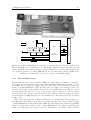
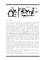
2. Der CMS Detektor
Das Design des CMS Detektors (siehe Abb. 1) fußt auf
• einem sehr guten und redundanten Muon Detektor
• optimal dazu angepaßten elektromagnetischen und hadronischen Kalorimetern
• einem hochauflösenden Spurdetektor
Das Design geht von einem 13 m langen und 6 m durchmessenden, supraleitenden Magnetsystem aus, welches das größte Element in Bezug auf Ausdehnung und Gewicht darstellt.
Das Muonsystem ist hierbei in das Magnetjoch integriert. Der Innendurchmesser des Magneten ist hinreichend groß, um sowohl das elektromagnetische als auch den größten Teil
des hadronischen Kalorimeters (HCAL) in sich aufzunehmen.
Das ECAL setzt sich aus 83 000 Blei-Wolframat (P bW O4 ) Kristallen zusammen, welche aufgrund ihrer kurzen Strahlungslänge ein kompaktes Design des ECALs bei hervorragender Schauertrennung erlaubt. Das HCAL ist als Kupfer(Messing)/Szintillator
Sandwichkalorimeter realisiert. Seine Stärke wächst von 6.6 auf über 10 Wechselwirkungslängen, von der Mitte zu den Endkappen hin, an.
II
Zusammenfassung
Abbildung 1: “Compact Muon Solenoid” Detektordimensionen und Layout [Della Negra
2002]
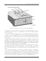
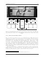
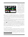
3. Der Spurdetektor
Der zentrale Silizium-Spurdetektor, welcher im Inneren der Kalorimeter installiert
wird, besteht aus einem inneren Pixel-Spurdetektor, der vom Silizium-Mikrostreifenspurdetektor SST (siehe Abb. 2) umschlossen ist. Dieser wiederum ist unterteilt in einen
Zylinderbereich und zwei Endkappen, welche den Kollisionspunkt mit 10, bzw. 9 Lagen
umschließen.
3.1 Die Detektormodule
Die Gesamtfläche, welche von den 15 232 SST-Detektormodulen aufgespannt wird,
umfaßt 210 m2 , was erst durch die Verwendung von 600 Wafertechnologie möglich wird.
Die nötigen Signal-zu-Rausch-Verhältnisse werden erhalten, indem Auslesechips mit extrem geringen Rauschanteilen entwickelt wurden. Weiterhin werden in den äußeren SSTBereichen, in denen die Streifenlängen bis zu 20.6 cm erreichen, Sensoren mit einer Dicke
von 500 µm verbaut, während die inneren Lagen 320 µm starke Sensoren verwenden.
Um den enormen Strahlenbelastungen von bis zu 1.6×10¹⁴ (1 MeV-equivalent n) / cm2
des 10-jährigen LHC Betriebes standhalten zu können, wird der SST bei −10 ◦C betrieben.
Dies reduziert sowohl die Dunkelströme der Sensoren, als auch das Reverse-Annealing,
welches hilft, die Verarmungsspannung der Sensoren nach der Bestrahlung klein zu halten. Aus diesem Grund werden auch nur Sensoren mit einer < 100 > Kristallstruktur und
hoher Resistivität verwendet. In dem n-dotierten Bulk sind p+ -Implantatstreifen eingelassen, welche über Polysilicon-Widerstände (nominal 1.8 MΩ) auf den Biasring geführt
werden. Die Auslese erfolgt über kapazitiv gekoppelte Aluminiumstreifen, welche in der
Breite über die p+ -Implantatstreifen hinausragen und somit eine höhere Spannungsfestigkeit ergeben. Die Rückseite der Sensoren ist aluminisiert, eine n+ -Schicht garantiert
einen guten Ohmschen Kontakt.
Die Sensoren werden auf U-förmigen Kohlefaserrahmen montiert, auf deren Beinen
Kaptonkabel zur Spannungsversorgung und Isolation aufgeklebt sind. Die Beine werden
an einem Ende von einem Querstück zusammengehalten, auf dem der Auslesehybrid und
der Pitchadapter (Streifenabstandswandler) aufgebracht sind.
Zusammenfassung
III
Abbildung 2: Dimensionen und Layout des zentralen Spurdetektors. Die Länge über
alles beträgt 5.4 m [Hartmann 2002]
3.2 Auslese und Steuerung
Im CMS-Spurdetektor findet ein uni-direktionales Takt- und Auslösesignal-Netzwerk
Verwendung, während die Steuersignale, wie z.B. Konfigurationsparameter, über ein bidirektionales Netzwerk übertragen werden. Diese beiden Netze sind als digital optische
Netzwerke realisiert, im Gegensatz zu dem Auslesepfad, welcher eine analog-optische Übertragung nutzt.
Auslesehybrid Die Auslesehybride vereinen die verschiedenen Chips, welche für den
Betrieb und die Steuerung der Module benötigt werden.
PLL∗ Der PLL-Chip regeneriert den Takt und das Auslösesignal, welche im CMS-Detektor
in einem gemeinsamen Signal kodiert übertragen werden, wobei die Auslösesignale als
fehlende Taktzyklen kodiert sind. Weiterhin synchronisiert der PLL-Chip die Phasenlage
des Taktsignals und kann das Auslesesignal verzögern, um so unterschiedliche Signallaufzeiten auszugleichen.
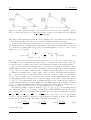
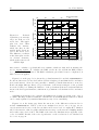
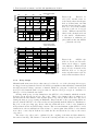
APV25† Der APV25-Chip ist das Herz der Auslesekette. Er ließt parallel 128 Detektorkanäle aus, verstärkt deren Signale und speichert diese analog zwischen (vgl. Abb. 3).
Der Vorverstärker und der anschließende Pulsformer sind direkt an eine analoge Pipeline angeschlossen. Auf diese folgt ein APSP-Filter, welcher das vom Vorverstärker und
Pulsformer gefaltete Signal zu entfalten vermag. Dies ist nötig, da der Vorverstärker
und Pulsformer das Eingangssignal auf etwa 100 ns verbreitert, was zu einem Signal in
mehreren aufeinanderfolgenden Takten führt. Dies läßt sich vermeiden, indem man das
Signal aus drei aufeinanderfolgenden Taktzyklen kombiniert und so im APSP-Filter die
Verbreiterung des Signals herausrechnet. Falls der APSP-Filter genutzt wird, spricht man
vom “Deconvolution”, falls er nicht genutzt wird vom “Peak” Modus. Weiterhin kann
zwischen dem Vorverstärker und dem Pulsformer eine Inverterstufe zugeschaltet werden,
um so unterschiedliche Eingangspolaritäten zu verarbeiten.
Die Daten der 128 Eingangskanäle werden über einen 128:1 Multiplexer seriell ausgegeben, wobei dessen Baumstruktur die Reihenfolge der Ausgangsdaten bestimmt. Vor
den Daten wird ein 12 -bit digitaler Datenkopf gesendet, welcher die Nummer der Pipelinezelle und ein Fehlerbit enthält. Eine Ausgabegeschwindigkeit von 20 MHz, damit halb
so groß wie die Taktfrequenz, ermöglicht ein nachgeschaltetes 2:1 Multiplexen von zwei
Auslesechips auf eine Datenleitung. Der APV25-Chip generiert alle 70 Taktzyklen ein
Synchronisierungsbit oder startet die Ausgabe von Daten, so ein Auslesesignal empfangen
wurde.
∗
†
phase locked loop
analogue pipeline voltage (build in a 0.25 µm process)
IV
Zusammenfassung
I2C
interface
bias voltage and currents
SCL
SDA
MUX
192 storage cells
x 128 channels
APSPs
shapers
calibration
logic
Analog Output
CLK
R/W cell pointer logic
timing
logic
T1
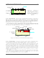
Abbildung 3: Blockdiagramm des APV25-Chips. Jeder Vorverstärker ist mit
einer 192 zellentiefen Pipeline verknüpft, welche die Auslesedaten für die Zeit
der Auslöseentscheidung zwischenspeichert. Der Zugriff auf die Pipeline wird von
einer Schreib-/Lesezeigerlogik kontrolliert, welche Zellen, die auf die Auslese warten,
entsprechend überspringt. Das vom Vorverstärker und Pulsformer gefaltete Signal kann
mittels eines APSP-Filters entfaltet werden, bevor es durch einen 128:1 Multiplexer und
das Auslesesystem übertragen wird. Zugriff auf die internen Register kann über eine I2CSchnittstelle erfolgen. Eine Kablibrationseinheit steht für Funktionstests zur Verfügung
[Heier 2001]
Die analoge Pipeline wird von einer Schreib-/Lesezeigerlogik verwaltet. Der Schreibzeiger eilt hierbei dem Lesezeiger immer um eine einstellbare Taktzahl voraus. Wird nun
ein Auslesesignal empfangen, wird die aktuelle Position des Lesezeigers zur Auslese in
einem FIFO-Speicher abgelegt. Dieser FIFO-Speicher hat eine Tiefe von 31 Zellen, wobei
im Deconvolution Modus jeweils drei Positionen für die Verarbeitung im APSP-Filter
gespeichert werden.
Weiterhin verfügt der APV25-Chip über eine interne Kalibrationseinheit, mit der unterschiedliche Ladungsmengen in den Vorverstärker eingekoppelt werden können. Die
Zeitspanne zwischen der Eingekopplung des Signals und dem Abtastzeitpunkt kann hierbei in Schritten von 3.125 ns variiert werden.
Der Auslesemodus und eine interne Kalibrationseinheit, sowie weitere Register des
APV25-Chips, werden über eine I2C-Schnittstelle kontrolliert. Mit der Auslösesignalleitung steht ein weiteres schnelles Interface zur Verfügung, welches Auslesesignale, Resetanweisungen oder Kalibrationsanfragen überträgt. Die verwendeten Muster haben hierbei
eine Länge von drei Bit. Dies, die Tiefe des Auslese-FIFO-Speichers und die Dauer der
seriellen Datenübertragung begrenzen die Auslesesignalrate.
APVMUX∗ Der APVMUX-Chip übernimmt das paarweise Multiplexen der APV25Chips auf eine gemeinsame Ausgabeleitung. Des Weiteren wandelt er das Stromsignal der
APV25-Chips in ein Spannungssignal um, wobei dieses über verschiedene Widerstände
erfolgen kann.
DCU† Der DCU-Chip integriert einen 12 -bit ADC mit I2C-Interface zur Messung verschiedener Umgebungsvariablen, wie die beiden Versorgungsspannungen auf dem Hybriden, den Gesamtleckstrom des Moduls oder die Temperatur eines Thermistor auf dem
Auslesehybriden.
∗
†
APV25 multiplexer
detector control unit
Zusammenfassung
V
3.3 Leistungsverhalten der Module
Die zu erwartenden Signalhöhen werden durch eine Landau-Verteilung beschrieben,
deren mittlerer Energieverlust durch die Bethe-Bloch-Formel für die verwendeten Teilchenenergien und das Absorbermaterial (Silizium) gegeben ist. Für minimalionisierende
Teilchen (MIPs) erwarten wir die Erzeugung von 23 500 Elektron-Loch-Paaren in 320 µm
starken Sensoren und 36 700 Elektron-Loch-Paare in 500 µm starken Sensoren. Entscheidend für den Betrieb des Spurdetektors ist ein hinreichendes Signal-zu-Rausch-Verhältnis
(SNR), auch nach 10 Jahren Betrieb. Da die Ladungssammlungseffizienz mit der Bestrahlung leicht abnimmt und der Leckstrom sowie der zugehörige Rauschanteil um mehrere Größenordnungen zunimmt, wird sich das SNR im Laufe des Betriebes deutlich verschlechtern.
Im Wesentlichen tragen drei verschiedene Quellen zum Rauschen bei. Diese sind das
sog. “Shot Rauschen”, welches z.B. in Halbleitern durch die statische Fluktuation der
Elektronemission verursacht wird, das sog. “Thermische Rauschen”, hervorgerufen durch
thermische Geschwindigkeitsfluktuationen der Ladungsträger und das “Flicker Rauschen”,
wofür Trapping/Detrapping Prozesse in Halbleitern bei DC-Strömen verantwortlich sind.
BIAS
RESISTOR
DETECTOR
SERIES
RESISTOR
Rs
AMPLIFIER +
PULSE SHAPER
ens
ena
Rb
Cd
inb
ina
ind
Abbildung 4: Equivalenter Schaltkreis zur Rauschanalyse [Hagiwara et al. 2002]
Alle diese Rauschquellen finden sich auch auf den Modulen wieder (vgl. Abb. 4). Hierbei unterscheidet man im Allgemeinen zwischen Rauschquellen, welche parallel und seriell
zum Vorverstärkereingang geschaltet sind. Parallel geschaltete Rauschquellen verhalten
sich wie Stromgeneratoren, während seriell geschaltete Rauschquellen als Spannungsgeneratoren modelliert werden. In Tabelle 1 sind diese Rauschanteile für SST Module des
Endkappenrings 6 bei −10 ◦C angegeben. Zusammen mit dem Signal von MIPs ergibt
sich ein SNR von 29.9 im Peak Modus und 19.2 im Deconvolution Modus.
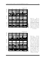
Rauschquelle
Leckstrom∗
Vorspannungswiderstand Rpoly
Auslesestreifenwiderstand Rs
Ausleseelektronik
Summe
Art
parallel
parallel
seriell
seriell
Peak Modus
8–1068
165
425
808
928–1415
Deconvolution Modus
3–480
74
627
1316
1460–1537
∗ skaliert von 0.1 µA für nichtbestrahlte Module auf bis zu 1 mA nach 10 Jahren LHC Betrieb
Tabelle 1: Rauschanteile für Ring-6-Module in äquivalenter Elektronladung. Berechnet
für Ts = 50 ns, inb = 0.05 µA – 1mA, homogen verteilt über alle 512 Auslesekanäle und
beide Sensoren, Rpoly = 1.85 MΩ, Rs = 220 Ω, Ctot = 15.6pF
4. Qualitätskontrolle für CMS Spurdetektormodule
Produktion und Bau der SST Module werden sich über einen Zeitraum von ca. zweieinhalb Jahren ziehen, wobei sich die Arbeiten auf über zwanzig verschiedene Institute
weltweit verteilen. Hierbei ist eine vollständige Qualitätskontrolle der gesamten Produktionskette essentiell, um Fehlerquellen frühzeitig zu erkennen und zu eliminieren. Hierzu
VI
Zusammenfassung
wird ein umfangreiches Qualitätssicherungsprogramm eingesetzt, welches sowohl Funktionalitätsprüfungen für alle elektronischen Komponenten beinhaltet, als auch umfangreiche Tests auf Sensorbasis. Letztere umfassen sowohl Qualifizierungstests, wie auch
Prozeß- und Bestrahlungskontrollen.
Die Detektormodule werden auf automatischen Montagerobotern mechanisch zusammengebaut, bevor sie in den Bondingzentren mit Industriebondern elektronisch vervollständigt werden. Da diese Module die kleinste unabhängige Detektoreinheit darstellen, ist
deren Qualitätsprüfung für die Gesamtqualität des späteren Spurdetektors mitentscheidend.
Im Rahmen der Detektormodulqualifizierung werden elektrische und mechanische
Tests durchgeführt. Während Letztere sich auf mechanischen Streß innerhalb eines Kühlzyklus von Raumtemperatur auf −10 ◦C beschränken, umfassen die elektrischen Tests eine
Vielzahl von Einzelmessungen. Hierbei spielen insbesondere Rauschmessungen, die interne
Kalibrationseinheit und Messungen mit externem Licht von IR-LED eine große Rolle.
Das Rauschen eines einzelnen Detektorkanals hängt primär von der an den Vorverstärker angeschlossenen Kapazität ab und ist damit sensitiv auf fehlende Bondverbindungen
und Kurzschlüsse zwischen mehreren Kanälen. Allerdings zeigen sich auch andere Streifenfehler im Rauschen, wie z.B Streifen mit erhöhtem Leckstrom oder mit fehlerhaftem Vorwiderstand. Um alle diese Fehlertypen eindeutig identifizieren zu können, ist insbesondere
die interne Kalibrationseinheit sehr hilfreich.
Kurzschlüsse der kapazitiven Koppelung der Auslesestreifen, sog. “Pinholes”, lassen
sich allerdings nur teilweise im Rauschen und der Kalibration identifizieren. Andererseits
können diese Kurzschlüsse nach Bestrahlung einen ganzen APV25-Chip mit seinen 128
Kanälen in Mitleidenschaft geziehen.
5. Die Karlsruher Teststationen
In Karlsruhe wurden zwei Stationen speziell für die Qualitätskontrolle von Spurdetektormodulen konzipiert, entwickelt und gebaut.
Die erste Station ist auf die Anforderungen einer schnellen Qualifizierung der Detektormodule nach dem Bonden optimiert. Obwohl hierbei ein voller thermischer Zyklus von
Raumtemperatur auf −10 ◦ C durchlaufen wird, ist es möglich mit der Rate des Bonders zu
testen, da die Station über eine entsprechende thermische Isolation und ein automatisch
steuerbares Kühlsystem verfügt. Der gesamte Aufbau dieser Station ist sehr kompakt
gehalten.
Die zweite Station ist auf tiefergehende Analysen von Modulfehlern ausgelegt. Hierbei ist es neben den normalen Analysen des Modulverhaltens auch möglich, weitere
Meßgrößen zu erhalten, indem Probenadeln, radioaktive Quellen oder Laser verwendet
werden. Das großzügig gewählte Volumen dieser Station erlaubt eine vielseitige Anwendung und kurzfristige Modifikationen. Beide Stationen verfügen über Szintillatoren und
Photomultiplier zur absoluten Eichung mit kosmischer Höhenstrahlung.
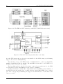
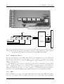
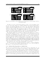
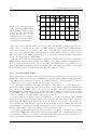
Das Auslesesystem besteht aus Komponenten, welche innerhalb der CMS Kolaboration entwickelt wurden, industriell verfügbar oder selbst entwickelt sind. Letztere umfassen wichtige Schlüsselkomponenten, wie die Takt- und Triggererzeugung, oder die Hochund Niederspannungsversorgung. Hierbei wurde für die Eigenentwicklung ein modulares
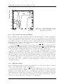
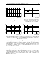
Konzept zu Grunde gelegt, welches auf einer Hauptplatine verschiedene funktionale Einheiten zusammenführt (vgl. Abb. 5).
Die Auslesesoftware basiert auf einem objektorientierten Ansatz, welcher in C++ auf
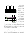
einer Linux-Plattform realisiert wurde. Für das Benutzerinterface und zur Steuerung
wird LabView verwendet. Auch bei der Softwareentwicklung wurde großer Wert auf Modularität gelegt und getrennte Funktionen in unterschiedlichen Bibliotheken abgelegt (vgl.
Abb. 6).
6. Testsystem Charakteristika und Qualitätsstudien
Eingehende Analysen von Detektormodulen setzen eine genaue Kenntnis von Testsystem und Testobjekt voraus. Hierbei werden insbesondere schon während der Entwicklungsphase des Auslesesystems erste Prototypen vermessen.
Zusammenfassung
VII
Repeater
Card
PM’s
Test Module
4 IR LED−arrays
T/H−Sensors
Peltier
I2C
PM−HV
LV for Peltiers
NIM logic
LV
Powerpack
LED Control
HV
Sequencer
Multiplexer
Interface card
Multi I/O
Peltier Control
Parallel port
Test station
Readout PC
FED
Motherboard
UPS
Abbildung 5: Die Karlsruher Teststationen bauen auf kleinen funktionalen Einheiten
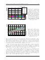
auf, welche entweder direkt vom PC aus betrieben werden oder auf einer externen Hauptplatine realisiert sind. Hierbei werden zentrale Funktionen, wie die Takt- und Auslösesignalerzeugung, von selbstentwickelten Komponenten übernommen
Graphical User Interface
Socket Connections
Analysis Thread
Filedump Thread
Shared Memory
Readout Thread
SlowControl Thread
APV−Lib
FED−Lib
Seq−Lib IR LED−Lib SlowControl−Lib
I2C−Lib
RAL−FED−Lib
Motherboard−Lib
Device Driver
Device Driver
Device Driver
Device Driver
FED−PMC
digital I/O card
parallel port
mulitf. I/O card
I2C−PMC
Abbildung 6: Die Struktur der Karlsruher Auslesesoftware basiert auf dem Linux Betriebssystem, für welches entsprechende Hardwaretreiber entweder entwickelt (I2C) oder
angepaßt (FED, MIO, DIO) wurden. Aufbauend hierauf sind die Funktionalitäten der
unterschiedlichen Komponenten in Bibliotheken abgelegt, auf welche die verschiedenen
Prozesse zugreifen. Die Steuerung erfolgt über eine graphische Benutzerschnittstelle (LabView), welche über TCP/IP angebunden ist.
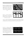
Zusammenfassung
# Entries
VIII
Entries
Mean
χ2 / ndf
Width
MP
Area
GSigma
30
25
641
21.22
59.64 / 72
1.752 ± 0.3362
19 ± 0.4266
430.3 ± 18.57
5.407 ± 0.5364
20
5
0
0
5
10
15
20
25
30
35
40
45
SNR
Module 30216630300027
10
Dec wo Inv Mode wo Cal
15
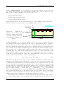
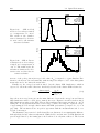
Abbildung 7: SNR im Deconvolution Modus bei einer Verarmungsspannung von 300 V
gemessen bei −10 ◦C. Die Breite der Verteilung wird vom Rauschen der Elektronik dominiert
Peak Modus
SNRM P
Korrekturfaktor
SNRKorr
RauschenM ess
ENCM ess
ENCT heo
ADC
34.53 ± 0.37
1.015
35.0 ± 0.4
1.97
986 ± 12
928
501 ± 33
Decon. Modus
minimale Korrektur
19.00 ± 0.43
1.075
20.4 ± 0.5
2.72
1691 ± 45
1460
621 ± 39
Decon. Modus
mittlere Korrektur
19.00 ± 0.43
1.180
22.4 ± 0.5
2.72
1540 ± 45
1460
566 ± 35
Tabelle 2: SNR Messung für Peak und Deconvolution Modi. Ein MIP in 500 µm starken
Sensoren (470 µm effektive Stärke) erzeugt 34 500 Elektron/Lochpaare. Die Messung der
wahrscheinlichsten Energiedeposition SNRM P und die akzeptanzkorrigierte Deposition
SNRcorr , verglichen mit dem berechneten Wert, zeigt eine gute übereinstimmung, welche
für eine absolute Kalibration der ADC Werte genutzt werden kann
Abbildung 7 zeigt das Signal-zu-Rauschverhältnis (SNR) im Deconvolution Modus.
Das SNR wird in diesem Fall durch Winkelakzeptanzen und die Auslöseimpulsakzeptanz
verbreitert, wobei insbesondere letztere großen Einfluß haben kann. Zeitgleiche Signale
von den Photomultiplieren werden hierbei direkt und den Sequenzer weitergeleitet, welcher
dann, entsprechend um Laufzeiten korrigiert, ein Auslesesignal für den Detektor und die
Auslese generiert. Hierbei kommt es zu zeitlichen Schwankungen, welche selbst bei optimaler Konfiguration zu Signalverlusten führen. Während der Peak Modus relativ unempfindlich auf diese Schwankungen reagiert (∼ 1.5 %), ist der Deconvolution Modus,
aufgrund seiner deutlich kürzeren Signalform, sehr empfindlich auf diese Schwankungen.
Hierbei kommt es zu einem durchschnittlichen Verlust von 7, 5 % bei optimalen Einstellungen, der bei einer Abweichung von nur 5 ns sich auf 18 % vergrößert.
In Tabelle 2 werden die gemessenen SNR Werte mit den vorhergesagten Werten aus
Tabelle 1 verglichen. Die Abweichung von der Vorhersage liegt im Peak Modus bei weniger
als 7 %, wohingegen die Abweichung im Deconvolution Modus stark von der Korrektur
abhängt. Bei minimaler Korrektur, ergibt sich eine Abweichung von ∼ 16 %, wohingegen
bei einer mittleren Korrektur (5 ns Fehler), die Abweichung auf ein 5 % Level abfällt.
Während normale Streifenfehler (Fehlende Bondverbindungen, Kurzschlüsse, unterbrochene Auslesestreifen) zu Ausfällen eines einzelnen Kanals führen, können Pinholes
Zusammenfassung
IX
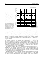
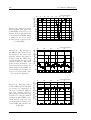
90
80
70
60
30
20
10
0
50
100
150
200
250
300
350
400
Leakage current [ µA]
01.1
40
Module 30200020000638
50
Peak w Cal wo Inv Mode
Calibration amplitude [ADC]
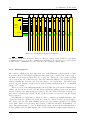
Abbildung 8: Pinholes und der APV25 Schaltplan
Abbildung 9: Die Kalibrationsamplituden für normale Kanäle sind unabhängig vom
Leckstrom. Anders bei Pinholedefekten: Hier regeniert sich das Kalibrationssignal bei
kleinen Leckströnem, bevor es bei Leckströmen von mehr als 30 µA wieder degeneriert
prinzipiell einen ganzen Auslesechip beeinträchtigen. Durch den Ohmschen Kurzschluß
der AC gekoppelten Auslesestreifen (siehe Abb. 8), liegt am dazugehörigen APV25 Eingangskanal das Potential Vimp an, welches den Vorverspärker in Sättigung treibt. Solange
das Eingangspotential kleiner als der virtuelle Ground von 0.75 V des Vorverstärkers
bliebt, bleibt sein Ausgang Vi positive und der Invertertransistor schaltet nicht durch.
Steigt das Eingangspotential allerdings über die 0.75 V so schalted der Invertertransistor durch, womit dieser permanent Strom zieht. Das Potential des Implantatstreifens
Vimp ist abhängig von dem Leckstrom, welcher durch den Vorspannungswiderstand RP oly
und einen Meßwiderstand auf der Rückführleitung Rret auf dem Auslesehybriden fliesst.
Abbildung 9 zeigt das Verhalten der Kalibrationsampliude bei eines APV25 mit einem
künstlich erzeugten Pinhole. Bei einem künstlichen Leckstrom von ca. 30 µA, wenn das
Eingangspotential Vimp mit dem virtuellen Ground des APV25 übereinstimmt, wird das
Pinhole im Signal der Kalibrationseinheit ununterscheidbar von normalen Kanälen.
Während ein einzelnes Pinhole die anderen Kanäle des APV25 nicht beeinflußt, ändert
sich dieses Bild drastisch, sobald mehr als drei Pinholes an einem APV25 angeschlossen
sind. Abbildung 10 zeigt das Verhalten eines APV25 mit unterschiedlich vielen Pinholes
anhand der Kalibrationspulse bei zunehmendem künstlichen Leckstrom. Hierbei reduziert
ein Leckstrom von mehr als 50 µA die Verstärkung des APV25 bei mehr als drei Pinholes um bis zu 30 %. Ursache hierfür ist, dass alle Inverterstufen über einen externen
Widerstand mit Spannung versorgt werden. Fliesst nun aber größerer Strom über diesen
Widerstand, so kommt es zu einem Spannungsabfall, welcher auf alle Kanäle des APV25
durchschlägt (vgl. auch Abb. 8).
Zusammenfassung
Mean calibration amplitude [ADC]
X
85
80
75
70
65
60
50
100 150 200
250 300 350
400
Leakage current
[ µA]
2
4
6
s
e
l
8
o
10
pinh
12
r of
e
b
Num
0
Abbildung 10: Pinhole verursachte Abnahme des APV25 Verstärkungsfaktors. Die
Antwort auf Kalibrationspulse mit einer ein MIP äquivalenten Amplitude kann als
Meßgröße für den APV25 Verstärkungsfaktor verwendet werden. Bei sehr niedrigen Leckströmen arbeitet der APV25 noch normal, welches von den geringen Potentialdifferenzen
in diesem Leckstrombereich herrührt. Mit steigendem Leckstrom aber, zeigt sich ein
Verstärkungsverlust von bis zu 30 % bei mehr als drei Pinholes
Extrapoliert man die Zahl der Pinholedefekte, wie sie in den Vorserien gefunden wurde,
auf die gesamte Produktion, so erwartet man, dass bei 3.5 % der Module ein APV25 mit
mehr als drei Pinholes verbunden ist. Hinzu kommt, dass auch mit leichten Kratzern
auf den Sensoren weitere Pinholes erzeugt werden können. Hierbei kommt zum Tragen,
dass bei den CMS Sensoren der Aluminium-Auslesestreifen breiter als das unterliegende
Implantat ist. Hierdurch trägt der Auslesestreifen prägnant zur Feldformung bei, welches
zu einer höheren Spannungsfestigkeit der Sensoren führt. Wird nun allerdings durch einen
Kratzer eine Spitze erzeugt, so ändert sich auch die Feldkonfiguration. Die resultierende
Feldspitze kann, insbesondere falls auch die Oxidschicht zwischen dem Implantat und dem
Auslesestreifen verletzt wurde, zu einem Durchbruch der isolierenden Kopplungskapazität
führen, welches dann in einem Pinhole endet.
7. Schlußfolgerungen
Die ersten Erfahrungen mit Prototypen des CMS Spurdetektors, verifizieren das robuste Design der Module. Die Zahl der rauschenden oder defekten Kanäle ist deutlich
unter der geforderten Quote von 2 %. Verbesserungen des Moduldesign ergeben sich aus
einem Randkanalrauschen, welches durch eine Filterkapazität deutlich reduziert werden
kann und aus der Sensitivität der APV25 auf DC-Kopplungen via Pinholes. Im letzteren
Fall wird die Spannungsversorgung modifiziert. Hierdurch wird die Empfindlichkeit auf
Pinholes der Auslesechip reduziert, allerdings besteht weiterhin die Notwendigkeit in der
Qualitätskontrolle alle Pinholes zu identifizieren und von der Auslese zu trennen. Beide
Änderungen erfolgen aufgrund der in Karlsruhe ausgeführen Messungen.
Die für die Produktion notwendigen Testsysteme und Prozeduren konnten anhand der
Prototypserien erprobt werden und erwiesen sich als außerordentlich erfolgreich.
1 Introduction
1
1
Introduction
To a great degree, the progress of particle physics has followed from progress in accelerator
science and instrumentation. There is no substitute for experiment, and experiment requires
both inventions in hardware and software as well as continuous innovation in analysis techniques. The slogan, “Yesterday’s sensation is today’s calibration and tomorrow’s background,”
(V. L. Telegdi) embodies both the challenge and the opportunity of advances in experimental
technique. In the middle of the revolution we are experiencing — indeed, making — in our
conception of Nature, when we deal with fundamental questions such as
• What are the symmetries of Nature, and how are they hidden from us?
• Are the quarks and leptons composite?
• Are there new forms of matter, like the superpartners suggested by supersymmetry?
• Are there more fundamental forces?
• What makes an electron an electron, a neutrino a neutrino, and a top quark a top quark?
• What is the dimensionality of spacetime?
we cannot advance without new instruments that extend our senses and allow us to create —
and understand — new experience far beyond the realm of everyday human knowledge.
The Large Hadron Collider (LHC) program addresses these questions and one of its detectors under construction is the “Compact Muon Solenoid” (CMS) detector with its Central
Tracker. Hereby the Silicon Strip Tracker (SST) alone will instrument an area of 210 m 2 with
15 232 individual detector modules of in total 15 different geometries.
A detector of this size can only be built in a collaboration of many institutes, all participating in an industrial like mass production. Over 20 institutes and companies worldwide
are involved in the Silicon Strip Tracker (SST) production, each of them specialised on one
or several steps of the production. Hereby, the Institut für Experimentelle Kernphysik of
the Universität Karlsruhe (TH) participates in sensor testing, wire bonding of modules, their
testing and their integration into larger substructures of the tracker end caps.
In Karlsruhe 1 600 modules will be bonded and tested. While the bonding is done on
an industrial automatic bonding machine, the test systems of the final modules have to be
developed by the collaboration. This contains not only the technical part, but also the test
strategies and the final automatisation, suitable for an usage of the test systems by technicians.
This thesis introduces all these aspects as well as the impact of the author’s work on the
testing procedures and the final design of the Silicon Strip Tracker (SST) module. In Sec. 2
a short overview of the Large Hadron Collider (LHC) physics program is given, followed by
a brief introduction to the “Compact Muon Solenoid” (CMS) detector design and its subdetectors. Thereafter in Sec. 4, the Silicon Strip Tracker (SST) is discussed in more detail. A
short description of the mechanics of SST modules and an introduction to the silicon sensors
is followed by a discussion of the readout chain. Hereby special emphasis is given to the
front-end hybrid (FEH) and its embedded chips, especially to the analogue pipeline voltage
chip (APV25). The different readout modes, and the signal processing as well as other specific
characteristics like the common mode (CM) suppression are introduced. The section is closed
by a discussion of the module performance, dealing with the signal creation as well as with
the noise behaviour.
Section 5 shows the different steps of the SST module production and the corresponding
quality control specifications. The latter are strongly influenced by the test results of the
2
first prototypes, performed in Karlsruhe. Those test results finally lead to the definition
of the official test procedures given in [Dirkes et al. 2002], culminting in an unique pinhole
tagging method, which utilised artifical leakage currents induced by infrared LEDs. Finally,
this section concludes with a detailed discussion of module faults, starting from general chip
failures and ending with an analysis of pinhole effects to the readout.
The following Sec. 6 is devoted to the test stations built for the module testing in Karlsruhe
and describes the hard and software developed. A description of the two different test systems
and their scope of application concludes this section.
In Sec. 7, the last section before the conclusion, an overview of the experimental results
and the module behaviour is given. After an analysis of the noise performance, the absolute
calibration of the test system using cosmic ray particles is shown. Based on this, systematic
studies of the modules performance in terms of signal-to-noise-ratio (SNR) are presented,
proving that the modules follow the expected performance. The last part of this section deals
with fault detection and shows the experimental signatures of the different module faults.
This results in the presentation of the discovered pinhole behaviour and its influence on the
final module design.
2 High Energy Physics at the Large Hadron Collider
2
3
High Energy Physics at the Large Hadron Collider
Among currently approved projects in high energy physics, the LHC has the unique potential, sufficient energy and luminosity, to probe in detail the TeV energy scale, relevant to
electroweak symmetry breaking to uncover and explore the physics behind it.
This study involves the following steps:
• Discover (or exclude) the single Higgs boson of the Standard Model (SM) and/or the
multiple Higgs bosons of supersymmetry
• Discover (or exclude) supersymmetry in essentially the full theoretically allowed mass
range
• Discover (or exclude) new dynamics at the TeV scale
The new high energy regime also offers a unique opportunity to look for the unexpected
physics, and new phenomena. There is a true multitude, with some perhaps less wellmotivated than others. Examples (always at the 1–10 TeV scale) are:
• Possible new electroweak gauge bosons with masses below several TeV.
• New quark or leptons.
• Extra dimensions with a mass scale for a few TeV.
The very high cross sections and resulting event rates make the LHC a true factory for
the production of particles like the top quark. Finally, high-rate phenomena can be used to
measure precisely the properties of Heavy Flavours. There is even some place for B physics,
at low luminosity, in particular sensitive studies of CP-violation in the B-hadron system will
be carried out.
2.1
Large Hadron Collider
The Large Hadron Collider (LHC) machine is a proton-proton collider that will be installed in
the 27 km circumference tunnel formerly used by the Large Electron Positron collider (LEP)
at the European Laboratory for Particle Physics (CERN). Hereby the LHC will extend the
accessible energy range by a factor of ten compared to the highest energy collider currently operating, the Tevatron. The LHC accelerator will use ∼ 1 100 superconducting dipole magnets
with a magnetic field of 8.4 T. Given the LEP circumference, this implies proton beams should
attain an energy of 7 TeV. The proton bunches in the machine are separated by 25 ns (with
an RMS length of 75 mm) and intersected at four points where experiments are placed. Two
of these are high-luminosity regions housings the “A Toroidal LHC Apparatus” (ATLAS) and
the CMS detectors. The other regions house the “A Large Ion Collider Experiment” (ALICE)
detector, to be used for the study of heavy ion collisions, and LHC-B (LHC-B), a detector
optimised for the study of b-flavoured hadrons. The beams cross at an angle of 200 µrad.
During the first year LHC will operate as proton-proton collider at a centre of mass energy of
√
s = 14 TeV with low luminosity, L = 10 33 cm−2 s−1 , which subsequently will be increased
to the design value of L = 1034 cm−2 s−1 . During the low luminosity phase the large nondiffractive inelastic cross-section of about 70 mb will already result in an average of ∼ 18
minimum bias interactions per bunch crossing in 25 ns time intervals. The interesting weak
physics signals are buried in this enormous background and will have to be disentangled by
selective and hierarchical trigger system. The weak signatures of new physics can show up
in a number of (sometimes complex) final states of leptons, jets and missing energy. This
4
2.2 Standard Model Higgs
puts extreme requirements on the performance of detectors: they must have good particle
identification, high count rate capability, good energy, momentum and angular resolutions for
charged leptons, jets, photons and missing transverse energy, which especially holds true for
the central tracking detectors.
2.2
Standard Model Higgs
The Standard Model (SM) as the combination of the Quantum Chromodynamics (QCD),
as theory of the strong interaction, and the electroweak interaction, as the unification of
Quantum Electrodynamics (QED) and weak interaction, has the group structure
S = SU (3)C ⊗ SU (2)L ⊗ U (1)Y .
(2.1)
Experiments over the past thirty years have shown numerous confirmations of the SU (2) L ⊗
U (1)Y electroweak theory: the existence of neutral currents, the necessity of charm, and the
existence and properties of the weak gauge bosons W ± and Z 0 . Experiments have also given
essential guidance to the form of the evolving standard model through the discovery of a third
generation of leptons (τ ; ντ ) and quarks (t; b). Finally, experiments have shown a number of
big surprises that have shaped both experimental and theoretical opportunities: the narrow0
ness of J/ψ and ψ 0 , the unexpectedly long B lifetime, the large degree of B 0 − B mixing,
the extreme heaviness of the top quark and evidence of neutrino oscillations.
Ten years of precision measurements have found no significant deviations from the predictions of the electroweak theory. A series of quite remarkable experiments, not to mention
the accompanying evolution in theoretical calculations, have tested the quantum corrections
of the electroweak theory — loop effects — to a precision of one per mil. The net result of
this prodigious effort is that we have found no evidence for new physics.
Nevertheless, we know that the Standard Model (SM) is incomplete and several problems
arising from the theory wait for experimental clues:
Hierarchy problem: what is the origin of the large difference between the electroweak
symmetry breaking scale and the Planck scale?
Fine tuning problem arises from quadratic divergences of the radiative corrections,
caused by the hierarchy problem
Why are there three generations of quarks and leptons
Neutrinos are described as massless particles in the SM, although neutrino oscillations
show, that they are massive particles
Still the SM has in total 19 parameters: the three coupling constants of the gauge theory
SU (3)C ⊗SU (2)L ⊗U (1)Y , three lepton and six quark masses, the mass of the Z boson, which
sets the scale of weak interactions, and the four Cabbibo-Kobayashi-Maskawa (CKM) (quarkmixing) parameters. One of the remaining two parameters, is a CP violating parameter,
associated with the strong interaction. The other parameter is associated to the mechanism
responsible for the breakdown of SU (2) L ⊗ U (1)Y to U (1)em . This can be taken as the mass
of the Higgs boson. The couplings of the Higgs boson are determined once its mass is given.
Unfortunately, within the SM we have no guidance on the expected mass of the Higgs
boson. The current (summer 2003) experimental lower bound is 114.5 GeV/c 2 . With larger
Higgs boson mass self coupling and coupling to the W and Z boson grow. This feature has
a very important consequence: either the Higgs boson must have a mass less than about
2 High Energy Physics at the Large Hadron Collider
5
800 GeV/c2 or the dynamics of W W and ZZ interactions, with centre of mass energies of the
order of 1 TeV, will reveal new structures.
The Higgs boson is an essential part of the analogy to the Meissner effect in superconductivity, that leads to an excellent understanding of the masses of the electroweak gauge
bosons W ± and Z 0 as consequences of the electroweak symmetry breaking. At tree level in
the electroweak theory, we have
√
2
MW
= g 2 v 2 /2 = πα/GF 2 sin2 θW ,
MZ2
2
= MW
/ cos2 θW
,
√
1
where the electroweak scale v = (GF 2)− 2 ∼ 246 GeV is set by the vacuum expectation value
of the Higgs field.
The problem is how to give mass to the weak gauge bosons, W ± and Z, without breaking
gauge symmetry, which is required for an renormalisable field theory. In order to understand
it, one may consider the weak interaction Lagrangian of the charged scalar field φ: i.e.
L=
† † h
→
−
i 1−
→
−
τ −
→
→
→ −
→
τ −
δµ φ + ig W µ φ − µ2 φ† φ + λ(φ† φ)2 − W µν W µν
δµ φ + ig W µ φ
2
2
4
(2.2)
where
−
→
−
→
−
→
−
→
−
→
W µν = δµ W ν − δν W µ − g W µ × W ν
(2.3)
−
→
is the field tensor for the weak gauge bosons W µ . The charged and the neutral W bosons form
a SU (2) vector, reflecting the non-Abelian nature of this gauge group, which is responsible
for the last term in Eq. 2.3 and leads to gauge boson self-interaction. Correspondingly the
−
→
gauge transformation on W µ has an extra term, i.e.
→
− →
−
φ → ei α · τ φ,
−
→
−
→
−
→
1 − →
α −−
α × W µ.
W µ → W ν − δν →
g
(2.4)
−
→
This ensures gauge invariance of W µν and hence for the last term of the Lagrangian, representing gauge kinematic energy. Evidently the middle term of Eq. 2.2, representing scalar mass
and self-interaction, is invariant under gauge transformation on φ. Finally the first term, representing scalar kinematic energy and gauge interaction, can be shown to be invariant under
the simultaneous gauge transformations (Eq. 2.4). However, the addition of a mass term
→
−
→ −
−M 2 W µ W µ
(2.5)
would clearly break the gauge invariance of the Lagrangian. In contrast the scalar mass term
µ2 φ† φ is clearly gauge invariant. This phenomenon is exploited to give mass to the gauge
bosons through back door without breaking the gauge invariance of the Lagrangian. This is
the Higgs mechanism of spontaneous symmetry breaking [Roy 2003].
Starting with a SU (2) doublet of complex scalar field φ with imaginary mass, i.e. µ 2 < 0,
results in the minimum of the scalar potential µ 2 φ† φ + λ(φ† φ)2 , to move out from the origin
to a finite value
p
v = −µ2 /λ,
(2.6)
i.e. the field develops a finite vacuum expectation value. Since perturbative expansion in
quantum field theory is stable only around a local minimum, one has to translate the field by
the constant quantity,
φ0 = v + H 0 (x),
(2.7)
6
2.2 Standard Model Higgs
g
q
g
q
t
q W, Z
t
H0
t
W, Z
t
H0
t̄
t
H0
q
q
q
g
g
t̄
H0
Figure 2.1: Higgs production in proton-proton high energy collisions is dominated by gluon
fusion
where the superscript denotes the electric charge. Thus one gets a valid perturbative field
theory in term of the redefined field H. It represents the physical Higgs boson, while the
three other components of the complex doublet field are absorbed to give mass and hence
longitudinal components to the gauge bosons.
Depending on the Higgs mass, different decay channels are optimal for signal detection.
2.2.1
Low-mass Higgs
For SM Higgs masses just above the LEP limit of M H > 114.5 GeV/c2 and below 2MW ,
the dominant decay mode is into bb (compare Fig. 2.2 on the next page), which is rather
unrealistic to extract, because there is no trigger for this process to disentangle it for the
enormous background of Quantum Chromodynamics (QCD) bb production.
For this reason the decay into γγ is the most promising in this mass region. Also the
branching ratio is very small and there is large background from pair production of photons
via qq → γγ, gg → γγ and bremsstrahlung processes. Excellent photon energy resolution is
required to observe this signal, which drives the very high quality electron calorimeter (ECAL)
development for ATLAS and CMS. For SM Higgs masses up to ∼ 140 GeV/c 2 , this channel
seems to be the most promising. A full coverage of this mass region requires a run at high
luminosity and detector performances as designed or better [Kunszt 1997].
If the Higgs boson is lighter than 130 GeV/c 2 , another promising channel arises from
its decay to a bb̄ pair in the tt̄H 0 channel [Drollinger et al. 2001]. In the channel t t̄H 0 →
`± νq q̄bb̄bb̄, where the Higgs Boson decays to bb̄, one top quark decays hadronically and the
second one leptonically.
The events are expected to show one isolated lepton, missing transverse energy E Tm and
six jets (four b-jets and two non-b-jets), but initial and final state radiation are sources of
additional jets. So the number of jets per event is typically higher than six. On the other
hand, not all six quarks of the hard process can be always recognised as individual jets in the
detector, in which case it is impossible to reconstruct the event correctly - even if there are
six or more jets.
For the reconstruction of resonances it is necessary to assign the jets of an event to the
corresponding quarks of the hard process. The nominal mass of the leptonically decaying W
boson, together with ETm and the lepton four momentum, is used to calculate two solutions of
the longitudinal momentum of the neutrino p Z (ν) which is needed for the mass reconstruction
of the leptonically decaying top.
Good mass resolution and the identification of b-jets is essential to reduce the number of
wrong combinations in the event reconstruction. A good mass resolution can be obtained
when the energy and direction of each reconstructed jet agree as closely as possible with
the quantities of the corresponding parent quark. The identification of b-jets is even more
important for efficient background suppression.
Branching Ratio
2 High Energy Physics at the Large Hadron Collider
7
1
.5
bb
WW
ZZ
.2
.1
.05
tt
ττ
gg
cc
.02
.01
2.2.2
100
200
300
500
mH0 [GeV]
Figure 2.2: Branching ratios for the
main decay modes of SM Higgs bosons
[Hagiwara et al. 2002]
Intermediate and high-mass Higgs
A second high precision discovery channel, offered by the SM, is ZZ (∗) decays into four charged
leptons (electrons and muons). This channel can be used for searching on a broad mass range
of MH ∝ 130–600 GeV/c2 . Below 2MZ , the event rate is small and the background reduction
more difficult, as one or both of the Z-bosons are off-shell. In this mass region the Higgs width
is small (. 1 GeV/c2 ) and so lepton energy and momentum resolution are of great importance
in maximising the significance of a signal.
Below the ZZ threshold, the main background arises from tt, Zbb and continuum ZZ ∗ /Zγ ∗
production. The tt background can be reduced by lepton isolation and pair invariant mass
cuts, which surely requires excellent vertex reconstruction. The Zbb background can be suppressed by isolation requirements. The ZZ ∗ process is an irreducible background.
The H → ZZ → 4` channel is sensitive over a wide range of SM Higgs masses from 2M Z
upwards: to about 400 GeV/c2 with 10 fb−1 and about 600 GeV/c2 with 100 fb−1 . For lower
SM Higgs masses, the width is quite small and precision lepton energy and momentum resolution are helpful; for larger masses the natural Higgs width increases. The main background
is continuum ZZ production, but the signal is very clean — this is considered as the “golden”
decay mode. With 100 fb −1 a signal in excess of six standard deviations is visible over the
entire range 200 < MH < 600 GeV/c2 . Experimentally an excellent vertex reconstruction
capability is required.
2.2.3
High-mass Higgs
As the SM Higgs mass increases further, its width and its production rate falls and one must
turn to decay channels with a larger branching ratio.
The first of these is H → ZZ → ``νν. Here the signal involves a Z decaying to lepton
pairs and a larger fraction of missing energy. Therefore the signal appears as a peak in the
missing energy spectrum. There are more potentially important sources of background in this
channel than in the 4` final state. In addition to the irreducible background from ZZ final
state, there are Z + jets events where the missing energy arises from neutrinos, cracks or
other detector effects that cause jet energies to be mismeasured.
8
2.3 Supersymmetry
Substantially larger event samples are available if the decay mode H → W W → `ν + jets
and H → ZZ → `` + jets can be exploited efficiently, which requires enormous reduction of
W + jets and Z+ jets background by kinematical cuts, which may be possible.
The LHC at full luminosity will be able to probe the entire range of Higgs masses from
lower limit set by LEP up to the value where it is no longer sensible to speak of an elementary
Higgs boson. Failure to find a Higgs boson over the range would therefore rule out the
SM. Then the Higgs sector either consists of non-standard Higgs bosons, or the electroweak
symmetry breaking occurs via some strongly coupled processes that will manifest itself in the
study of W W scattering.
2.3
Supersymmetry
In the supersymmetric standard model, a doubling of the particle spectrum is predicted. For
every particle that has been discovered, supersymmetry predicts a supersymmetric partner
that has not discovered yet. The extra particles circulate in loops and protect the hierarchy
from quadratic divergences.
But supersymmetry can not be exact, otherwise the particles and their superpartners
would be degenerate in mass, which is clearly not the case. But even with a broken symmetry
— different masses for particles and their superpartners — the radiative correction from
virtual boson and fermion loops are of opposite sign. Thus, since the particles and their
supersymmetric partners are assumed to have the same couplings, the one-loop divergences
will cancel.
The most widely quoted scheme is that of the Minimal Super-Symmetric Model (MSSM),
which consists of taking the SM and adding the corresponding supersymmetric partners. In
addition the MSSM contains two hypercharge Y = ±1 Higgs doublets, which is the minimal
structure for the Higgs sector of an anomaly free supersymmetric extension of the SM. Furthermore, the supersymmetric structure of the theory requires (at least) two Higgs doublets
to generate mass for both “up”-type and “down”-type quarks (and charged leptons), which
leads to (at least) five supersymmetric Higgs bosons: one lightest CP even h 0 , one heavier CP
even H 0 , one CP odd A0 and two charged H ± as it is described in [Kazakov 2000].
If supersymmetry is realised by nature and connected to the SU (2) symmetry breaking of
the electroweak interaction, the LHC will be able to find traces of it. For the MSSM Higgs
sector the LHC covers nearly all the theoretical allowed parameter space, although ensuring a
5σ discovery over the entire plane requires more luminosity [Womersley 1997]. Furthermore,
if supersymmetry is relevant to the electroweak symmetry breaking problem, then most of
the supersymmetric particles will be in a mass range that is observable at LHC. Both ATLAS
and CMS have enormous potential to discover supersymmetry, if it exists at mass scale less
than about 2 TeV [Asai 2002].
2 High Energy Physics at the Large Hadron Collider
2.4
9
New Physics
Beside the search for Higgs bosons, also other theoretical models will be probed at the LHC.
This includes
• New gauge bosons as they are a generic prediction of superstring theories, which have
additional U (1) gauge groups, motivating the search for additional W 0 and Z 0 bosons
• Technicolor as a model of strong electroweak symmetry breaking predicts resonances
which decay into vector bosons. These signals are very striking since they are produced
with large cross sections and may be observed in the leptonic decay modes of the W
and Z where the backgrounds are very small
√
• Strongly interacting W ’s will reveal new dynamics at a scale of s = 1 TeV, if no
Higgs-like particles exists
• Compositeness of the quarks and leptons has no a priori reason, but could explain the
observed mass spectrum. If they have a substructure it will be revealed in the deviations
of the jet cross-section from that predicted by QCD
2.5
B Physics
The exploration of physics with b-flavoured hadrons offers a very fertile testing ground for
the SM description of electroweak interactions. One of the key problems to be studied is the
phenomenon of CP violation, which, although already discovered in 1964 by Christenson et.
al. in the neutral Kaon system [Christenson et al. 1964], is still one of the experimentally
least constrained phenomena. Another main topic is the study of rare b decays, induced by
flavour changing neutral currents (FCNCs) transitions b → s, d, which are loop-suppressed in
the SM and thus very sensitive to new-physics effects. During the last few years, B physics
has received a lot of attention, both from theorists and experimentalists, and we are presently
at the beginning of the B-factory era in particle physics. The BaBar (SLAC), BELLE (KEK)
and HERA-B (DESY) detectors as well as CLEOIII (Cornell), CDF-II and D0-II (FermiLab)
have already seen their first events, and although the physics potential of these experiments is
very promising, it may be that the definite answer in the search for new physics in B decays
will be left for second-generation B experiments at hadron machines. Already during the low
luminosity phase, 1012 –1013 b-events will be produced at the LHC. Previously existing doubts
regarding the possibility to reconstruct B hadrons in the very complicated topology at hadron
machines have been dispelled by the Collider Detector FermiLab (CDF) collaboration, which
also demonstrated the key role of tracker and vertex systems for B physics.
Theoretical background In the SM with SU (2) ⊗ U (1) as the gauge group of electroweak interactions, both the quarks and leptons are assigned to be left-handed doublets and
right-handed singlets. The quark mass eigenstates are not the same as the weak eigenstates,
and the matrix relating these bases was defined for six quarks, given an explicit parametrisation by Kobayashi and Maskawa [Kobayashi and Maskawa 1973] 1973. This generalises the
four-quark case, where the matrix is described by a single parameter, the Cabibbo angle θ C
[Cabibbo 1963]. By convention, the mixing is often expressed in terms of a 3 × 3 unitary
matrix V operating on the charge −e/3 quark mass eigenstates (d, s, and b):
0
Vud Vus Vub
d
d
d
s0 = Vcd Vcs Vcb · s ≡ V̂CKM · s .
(2.8)
Vtd Vts Vtb
b
b
b0
10
2.5 B Physics
Figure 2.3: The unitarity triangle. The version on the left uses the definition given in
Eq. 2.8 on the preceding page, while the rescaled version on the right uses the definition
of η and ρ [Ellis 2001]
The values of individual matrix elements can, in principle, all be determined from weak decays
of the relevant quarks, or in some cases, from deep inelastic neutrino scattering.
As far as phenomenological applications are concerned, the following parametrisation of
the CKM matrix, the “Wolfenstein parametrisation” [Wolfenstein 1983], which corresponds
to a phenomenological expansion in powers of the small quantity λ ≡ |V us | = sinθC ≈ 0.22,
turns out to be very useful:
V̂CKM
λ
Aλ3 (ρ − iη)
1 − 12 λ
+ O(λ4 ),
−λ
1 − 21 λ
Aλ2
=
Aλ3 (1 − ρ − iη) −Aλ2
1
(2.9)
where A, ρ and η are real numbers, that were intended to be of the order of unity. However,
in the LHC era, the experimental accuracy will be so tremendous that one has to take into
account the next-to-leading order terms of the Wolfenstein expansion [Kowalewski 2003].
The relations dictated by unitarity allow a convenient geometrical representation of the
CKM parameters. The product of any row (column) of the matrix times the complex conjugate
of any other row (column) results in three complex numbers that sum to zero, and can
be drawn as a triangle in the complex plane. There are three such independent triangles.
Two of the three have one side much shorter than the others (i.e. have one side that is
proportional to a higher power of λ than are the others), but the remaining triangle, formed
by multiplying the first column by the complex conjugate of the third column, has all sides
of order λ3 . It is this triangle that is usually discussed when considering the impact of
experimental measurements on the parameters of the CKM matrix. These unitarity relations
need to be verified experimentally; a violation of unitarity would point to new physics (e.g. a
fourth generation, in which case the 3 × 3 submatrix need not be unitary).
∗ + V V ∗ + V V ∗ = 0, is usually rescaled
The unitarity triangle of interest, namely V ud Vub
cd cb
td tb
∗
by dividing through by Vcd Vcb , giving a triangle whose base has unit length and lies along
the xaxis and
whose apex,
in terms
of the parameters λ, A, ρ and η and using the definition
λ2
λ2
ρ = 1 − 2 ρ and η = 1 − 2 η , is at (ρ, η) up to corrections of order λ 2 . By dividing
out Vcb we largely eliminate dependence on the parameter A, which is in any case relatively
well known (A = 0.85 ± 0.04). The angles of the unitarity triangle are
Vtd Vtb∗
α = arg −
∗ ,
Vud Vub
(compare Fig. 2.3).
Vcd Vcb∗
β = arg −
,
Vtd Vtb∗
∗ Vud Vub
γ = arg −
.
Vcd Vcb∗
(2.10)
2 High Energy Physics at the Large Hadron Collider
b̄
W+
d
W−
d¯
11
b̄
t̄
d¯
b
t
b
d
0
Figure 2.4: B 0 – B transition diagrams
An invariant measure of the size of the CP violation in the CKM matrix is given by the
Jarlskog invariant
J = c12 c23 c213 s12 s23 s13 sinδ = A2 λ6 η
(2.11)
where cij and sij are shorthand for the cosine and sine of the angle θ ij (see e.g. [Hagiwara et al.
2002] for the corresponding “standard” parametrisation), and A, λ and η are the parameters
of √
the Wolfenstein parameterisation. The maximum value of J in any unitary 3 × 3 matrix is
(6 3)−1 ∼ 0.1; the value in the CKM matrix is ∼ 4 × 10 −5 , which underlies the statement
that CP violation in the SM is small.
2.5.1
0
The Mass Difference ∆mB and B0 –B Mixing
0
The eigenstates of flavour, B 0 = (bq) and B = (bq) (q = d, s), degenerate in pure QCD,
mix on account of weak interactions (box diagrams of Fig. 2.4). The quantum mechanics of
0
the two-state system, with basis {|1i, |2i} ≡ {|B 0 i, |B i}, is described by a complex, 2 × 2
Hamiltonian matrix
i Γ Γ12
i
M M12
−
H=M− Γ=
(2.12)
∗
M12
M
2
2 Γ∗12 Γ
with Hermitian matrices M and Γ and for the case that CPT theorem holds. The off-diagonal
elements in Eq. 2.12 arise from ∆B = 2 flavour changing transitions with virtual (M 12 ) or
real intermediate states (Γ12 ), in the latter case corresponding to decay channels common to
0
B 0 and B .
Diagonalising Eq. 2.12, the physical eigenstates B h (’heavy’), Bl (’less heavy’) and the
corresponding eigenvalues Mh,l − 12 Γh,l are obtained. The mass and width difference read
∆mB ≡ Mh − Ml = 2|M12 |,
∆Γ ≡ Γh − Γl =
∗ Γ )
2Re(M12
12
.
|M12 |
(2.13)
0
The mass difference ∆mB is a measure of the frequency of change from B 0 into a B or vice
versa. Measurements give an average ∆m B = (3.07 ± 0.12) × 10−4 eV, which is a hundred
times larger than the corresponding ∆m K in the Kaon system.
Once the neutral B mesons are produced in pairs, their semileptonic decays (inclusive or
0
exclusive) provide an excellent method to measure the B 0 –B mixing. From their respective
0
quark contents, B 0 decays into a positive charged lepton ` + while B goes into a negative `− .
0
0
If B 0 and B do not mix, the produced pair B 0 +B would have a distinctive signature of a
dilepton with opposite signs `+ +`− . Therefore, a fully reconstructed µ + +µ+ same sign event
0
would unambiguously demonstrate the conversion of a B into a B 0 , requiring a sufficient
tracking precision to reconstruct the secondary and primary vertices unambiguously.
0
For the neutral B 0 and B system, the off-diagonal term Γ12 is extremely small since
0
the overlap in the decay products of B 0 and B is rare. Indeed, the B 0 decays mostly into
0
anti-charmed and unflavoured particles described by b → c + d + u, while the B decays into
12
2.5 B Physics
charm from b → c + d + u. These final decay products are completely distinct. There exist
0
only a few common channels into both B 0 and B decay. There are B 0 → D + + D − ( or
0
π + + π − ) ← B coming from b → c + d + c (or b → u + d + u). However, their rates are
suppressed by |Vcb Vcd |2 (or |Vub Vud |2 ). Experimentally only an upper bound < 10 −3 is known
for the branching ratio into common decay channels.
2.5.2
CP Violation in the B System
0
Similar to the Kaon system, the B 0 and B are mixtures of CP eigenstates, B1 = (B 0 −
0 √
0 √
B )/ 2 and B2 = (B 0 + B )/ 2 of eigenvalues ±1 respectively:
1
0
Bl = pB 0 + qB = p
(B2 + B1 )
1 + ||2
1
0
Bh = pB 0 − qB = p
(B1 + B2 )
1 + ||2
q
∗ − i Γ∗
∗ − i Γ∗
M12
M12
p
1−
2 12
2 12
= q
=
=q
q
1+
i
∗ − i Γ∗
M12
M12 − 2i Γ12
2 12 M12 − 2 Γ12
(2.14)
0
Indirect CP violation in B 0 –B mixing arises if
p
6= 1 −→ 6= 0
q
(2.15)
which results from the fact that the physical flavour eigenstates B h and Bl are different from
the CP eigenstates B1 and B2 .
2
Taking the time-depended decay rate Γ(B 0 (t) → f ) = Nf hf |B 0 (t) of an initially tagged
B 0 into some final state f , where Nf is time independent normalisation factor, leads to the
decay amplitudes
2
2
0
Af = hf |B (t) ,
(2.16)
Af = hf |B 0 (t) ,
0
where Af corresponds to the decay rate of B . If the final state f is a CP eigenstate, with its
CP conjugate state f, Af and Af are defined in the corresponding way. Finally the quantity
λf =
q Af
p Af
(2.17)
plays a central role in CP asymmetries and other observables in B mixing. The three quantities
A q
f
,
λf
(2.18)
,
p
Af are independent of phase conventions and the only complex quantity here is λ f . Its phase is
a physical observable. If any of these quantities is not equal to 1 (or −1 for λ), then CP is
violated in the particular decay.
CP violation in mixing (|q/p| 6= 1) If |q/p| 6= 1, then CP is violated, which is called CP
violation in mixing, or indirect CP violation, because the mass eigenstates are different from
the CP eigenstates or in other words |B h i and |Bl i are not orthogonal and CP is not conserved
in |∆B| = 2 amplitudes.
2 High Energy Physics at the Large Hadron Collider
13
CP violation in decay (|Af /Af | 6= 1) If |Af /Af | 6= 1, then CP is violated, which is called
CP violation in decay, or direct CP violation. It occurs due to interference between various
terms in the decay amplitude, and requires that at least two terms differ in both their strong
and in their weak phases.
CP violation in the interference between decay and mixing (λ f 6= ±1) The third
type of CP violation is possible in neutral B decay into CP eigenstate final state, f CP . If CP is
conserved, then not only |q/p| = 1 and |A f /Af | = 1, but the relative phase between q/p and
Af /Af also vanishes. If not, this is called CP violation in the interference between decays with
and without mixing, because it results from the CP violation interference between B 0 → fCP
0
and B 0 → B → fCP .
Measuring CP
The most promising method of measuring CP violation is to look for
0
an asymmetry between Γ(B 0 → fCP ) and Γ(B → f CP ), where fCP is a hadronic state having
a well-defined CP eigenvalue ±1. Commonly used are two particle systems like φ + K S (CP
parity = −1), π + + π − (CP parity = +1), and ρ0 + KS (CP parity = −1).
The “golden mode” for studying CP violation in B decays is B 0 → J/ψKS0 . In this case
the decay is dominated by the tree level diagram with internal W → cs emission, leading to
(bd) → cW + d → (cc)(sd). This is not a flavour-neutral state at the quark level, but becomes
so at the hadron level through K 0 mixing. For this decay one finds
∗
∗
∗
Vcd Vcs
Vtb Vtd
Vcs Vcb
λfCP = ηCP
(2.19)
V tbVtd∗ B mixing V csVcb∗ decay V cdVcs∗ K mixing
Im(λfCP ) = ηCP sin 2β
(2.20)
with very little theoretical uncertainty [Kowalewski 2003]. The CP eigenvalue η CP is −1 (for
B 0 → J/ψKL0 it is +1). This decay mode is also favourable experimentally. The product
branching fraction B(B 0 → J/ψKS0 )B(J/ψ → `+ `− ) ' 5 × 10⁻⁵ is well within the reach of B
factories, and the final state includes a lepton pair, enabling excellent background suppression.
The experimental determination of sin 2β involves three key elements:
• The reconstruction of the CP eigenstate, J/ψK S . This requires good momentum and
energy resolution for charged particles and photons.
• The determination of the b quark flavour of the recoiling B meson at the time of its
decay, which requires good particle identification in order to cleanly identify the charged
Kaons and leptons that are used to infer the b quark flavour.
• The determination of the difference between the decay times of the B decay to the
CP eigenstate and the recoiling B, requiring excellent vertex resolution to extract the
spatial distance between the decay points of the two B mesons.
The BaBar and Belle experiments first observed non-zero CP violation in 2001 and have
now measured sin 2β with good precision
sin 2β = 0.719 ± 0.074 ± 0.035
sin 2β = 0.741 ± 0.067 ± 0.034
(Belle)
(2.21)
(BaBar)
(2.22)
The systematic errors are dominated by the statistics of the auxiliary samples used to evaluate
them, and should continue to fall with increasing luminosity. The combined precision of the
14
2.6 Heavy Ion Collisions
experiments will be impressive at the start of LHC, but nonetheless, the huge statistics of the
LHC can bring valuable new insights to this important channel.
There is presently substantial effort on determination of the angle α. This angle is accessible in b → u transitions leading to uudd final states, e.g. B 0 → π + π − . In contrast
to the golden mode, however, there are both tree and penguin decay amplitudes that contribute appreciably to these decays, rendering the precise determination of α is more difficult.
The experimental situation is also less favourable, due to the very small branching fractions (B(B 0 → π + π − ) ' 5 × 10⁻⁶ ), higher backgrounds and the difficulty in distinguishing
B 0 → π + π − decays from the more numerous B 0 → K + π − decays.
The e+ –e− B-factories, BaBar and Belle, operating at the Υ(4S) resonance will not be in
a position to explore the BS system. Since it is, moreover, very desirable to have large data
samples available to study BS decays, they are of particular interest for hadron machines like
the Tevatron (at low statistics possible) and LHC [Wilkinson 2000].
Experimentally, the BS → J/ψφ channel has a clean signature and very big samples
will be available. The SM prediction for the CP asymmetry in this channel is very small:
A ∼ −2λ2 η ∼ O(few %), where λ and η are the Wolfenstein parameters of the CKM matrix.
A large observed asymmetry would therefore be a sign of new physics. Good proper-time
resolution is essential given, the rapid oscillations of the asymmetry [Ellis 2001].
2.6
Heavy Ion Collisions
Heavy ion beams at LHC will provide collision energy densities well above the threshold for
formation of quark gluon plasma (QGP). ALICE, as a dedicated experiment for heavy ion
physics, is part of the LHC program and ATLAS as well as CMS have good capabilities for a
heavy ion program [Wrochna 2002].
3 Compact Muon Solenoid
3
15
Compact Muon Solenoid
The concept of a compact detector for the LHC based on a solenoid, the CMS detector, was
presented for the first time during the LHC Workshop in Aachen in October 1990. Basic ideas
are an optimised muon detection system, reached through a very strong magnetic field and a
compact detector design including tracking and calorimetry. The choice of a superconducting
solenoid generating a magnetic field of 4 Tesla strength is a pre-requisite for good momentum
resolution even for high momentum (muon) tracks (≈ 1 TeV) up to pseudo-rapidities of 2.5.
Following on the formation of a proto-collaboration for CMS in May 1991, the Letter of
Intent (LoI) based on a conceptual design of the complete detector was signed and submitted to the LHC Committee (LHCC) in October 1992. With the Technical Proposal [CMS
Collaboration 1994] (1994) the design phase was finished and detailed Research & Development (R&D) studies during the following years led to the publication of the Technical Design
Reports of the individual sub-detectors [CMS Collaboration 1997a,b,c,d, 1998].
In 2000 there was a major design change for the Tracker Project. The micro-strip gas
chambers (MSGCs) in the outer part of the tracker were replaced by an all-silicon solution.
3.1
Detector Design Goals
The design baseline of CMS was driven by
• a very good and redundant muon system, superimposed on a solenoid
• best possible ECAL consistent with the muon system
• a high quality central tracking to achieve both points above
• and of cause to be a financially affordable detector
The large radius of 6.0 m of the chosen solenoid allows a full calorimetry located inside the
solenoid. From the LEP experiments it is well known that very precise electromagnetic
calorimetry is essential for separation of photons from decays, for example from low mass
Higgs bosons. Such a precision calorimetry fits naturally in the CMS design.
Figure 3.1 on the following page shows an overview of CMS. The individual sub-detectors
are discussed in the following sections.
3.2
Magnet System
The choice of the magnet system meant the starting point of the CMS detector design. A long
superconducting solenoid of 12.5 m length and 6.0 m inner diameter, with a uniform magnetic
field of 4 T has been chosen. The magnetic flux is returned via a 1.8 m thick saturated iron
yoke which is instrumented with muon detector stations. The inner coil diameter is large
enough to accommodate the tracker and calorimeters.
Since the magnet is the main element of CMS in terms of size (21.6 m length, 15 m diameter), weight 12 500 t, and structural rigidity, it is used as the principal structural element
to support all other detector components. The return yoke consists of five outer barrel rings
and two end-caps with three separated disks both. Each barrel ring is made up of three iron
layers. The superconduction coil system and its sub-systems (cryogenics, power, vacuum and
quenching protection) are attached to the fixed central ring. The other rings can slide on rails
parallel to the beam direction, to allow insertion and maintenance of the muon stations. For
details on the magnet system see the [CMS Collaboration 1997c] and recent publications like
[Herve et al. 2001].
16
3.3 Central Tracker
Figure 3.1: “Compact Muon Solenoid” detector dimensions and layout [Della Negra 2002]
3.3
Central Tracker
The innermost part of the CMS
detector is the Central Tracker, which
is divided into the Pixel and Strip
Tracker (see Fig. 3.2). Initially it was
planed to use MSGCs for the outer
part of the Strip Tracker, but in 2000,
the design baseline was changed to an
all-silicon solution, although the
MSGCs had passed all milestones and
showed their viability of stable tracking within a LHC experiment. Main
argument towards an all-silicon solutions was the chance to concentrate
all available effort to a common type
of detectors, the reduced price for sil- Figure 3.2: Central Tracker dimensions and layout.
The overall length is 5.4 m [Hartmann 2002]
icon as well as an easier replacement
of detector elements or upgrade. The Central Tracker is described by detail in Chapter 4.
3.3.1 Pixel Vertex Detector
The most interesting events at the LHC are likely to contain several b-jets originating from
the decay of heavy particles. In order to allow efficient tagging of these jets as well as of other
objects (c, τ ) the tracking must extend most closely towards the reaction vertex. The high
3 Compact Muon Solenoid
Figure 3.3: Pixel detector layout.
The barrel length is 52 cm [Kotlinski
2002]
17
Figure 3.4: Construction principle of
a pixel detector with bump bonded
readout electronics [CMS Collaboration 1998]
flux of particles necessitates appropriate pixel size to keep the occupancy sufficiently low. On
the other side, the pixel size is influenced by the area needed for the readout chip for the pixel
analogue front-end and readout circuit. Furthermore, material budget and sufficient cooling
had to be kept in mind, while designing the pixel detector.
The pixel detector consists of three barrel layers at mean radii of 4.3, 7.3 and 11.0 cm. The
two innermost layers will be installed directly, while the third one will be added before start
of the high luminosity phase of LHC. The pixel barrel will be 52 cm long and supplemented
by two end disks each side (see Fig. 3.3).
In order to achieve optimal vertex position resolution in both the (r, ϕ) and the zcoordinates, a design with a square pixel shape of 150 × 150 µm 2 was adopted. To enhance
the spatial resolution by analogue signal interpolation, the use of charge sharing induced by
the large drift (Lorentz angle 28◦ at 4 T for electrons) is made. Hence, the detectors are
deliberately not tilted in the barrel layers but titled in the end disks, resulting in a turbine
like geometry.
The whole pixel system consists out of about 1 400 detector modules arranged into 4
module ladders in the barrel and 7 module blades in the disks. To readout the detector,
about 16 000 readout chips are bump-bonded to the detector modules (see Fig. 3.4). The
total number of readout channels (pixels) is about 45 × 10 6 . The pixel detectors uses a
readout system with zero-suppression to reduce the amount of data to be transfered.
At full LHC luminosity about 1 000 tracks cross the pixel barrel layers every 25 ns, which
translates into an occupancy of 3.3 × 10 −4 or a single pixel counting rate of 10 kHz.
3.3.2
Silicon Strip Tracker
The SST surrounds the pixel system. In the central pseudo-rapidity region detectors are
arranged in a barrel geometry with 10 layers, while in the forward regions they are arranged
in 9 disks, radially segmented into the so called petals. Furthermore, 5 stereo layers are
concentrated below a radius of 90 cm. The detector modules are assembled using single sided
sensors with the strips parallel to the beam axis in the centre or barrel region and with the
strips orthogonal to the beam, nominally pointing to in the two end-cap regions. Figure 3.5 on
the following page shows a longitudinal view of the all-silicon CMS tracker.
The overall instrumented area of the silicon strip tracker will cover 210 m 2 . The possibility
to construct such a large silicon tracker relies crucially on a few key elements like the usage of
600 wafer technologies and implementation of the front-end readout chip in deep sub-micron
18
3.3 Central Tracker
Figure 3.5: Strip Tracker layout. Solid lines represent double sided modules [CMS Collaboration 1998]
technology with improved signal-to-noise-ratio (SNR) performance. This enables usage of
large area modules in the outer part of the tracker. Modules with strip length of up to
20.6 cm, comparing to 12.3 cm in the inner part, produce 50 % more noise. This will be
compensated by increasing the sensors thickness from 320 µm, as used in the inner layers, to
500 µm in the outer ones resulting in the same SNR. Pitches range from 80 µm to 183 µm in
the barrel and 80.5 µm to 205 µm in the end-caps.
The stereo layers are built out of two completely independent single-sided detection units
mounted back to back; one of them precisely measures the main coordinate, the other rotated
by 100 mrad with respect to the first, gives a sufficient measurement of the second coordinate.
The tracker has to operate in a high radiation environment for at least 10 years, maintaining a satisfactory global performance despite expected changes in the material characteristics
due to irradiation. The level of irradiation coming from primary interaction will be very high
around the collision region; in addition a high flux of backscattered neutrons evaporated from
nuclear interactions in the material surrounding the tracker will be present. The innermost
layer of the SST will undergo a fluence of 1.6 × 10 14 (1 MeV-equivalent n) / cm 2 during 10
years of operation.
To avoid potentially critical degeneration of the sensor performance due to irradiation,
the SST will be kept at −10 ◦ C. This will drastically reduce the sensor dark current and,
consequently, the risk of thermal runaway of detector modules. Furthermore, keeping the
irradiated sensors at low temperature substantially reduces the reverse annealing effect [Moll
1999] and helps keeping the depletion voltage below a reasonable level.
Crucial for track finding is mainly the number of detectors intersected on the one side,
and the overall material budget on the other side, because all material inserted will cause
multiple scattering, which reduces the track quality (see Figs. 3.6 and 3.7 on the next page).
Critical regions are the gaps between barrel and end-caps and the high pseudo-rapidity regions.
However, the average hit multiplicity within the Silicon Strip Tracker is at least eight for tracks
of infinite momentum and |η| < 2.4 where four of these come from double-sided detectors
(refered as 3D in Fig. 3.6 on the facing page).
3 Compact Muon Solenoid
Figure 3.6: Average number of detectors intersected by infinite momentum tracks as function of pseudorapidity for the silicon strip tracker
[Caner 2001]
3.4
19
Figure 3.7: Contributions of the CMS
tracker subsystem to the interaction
length. The label ’outside’ refers to
all material installed beyond to active
volume of the tracker [Caner 2001]
Calorimeter
The CMS detector utilises three calorimeters: the innermost is the ECAL, placed together with
the main part of the hadronic calorimeter (HCAL) inside of the magnet coil. Furthermore,
the HCAL has two forward extensions, installed 11 m up- and downstream of the interaction
point.
3.4.1
Electromagnetic Calorimeter
CMS has made precision electromagnetic calorimetry a priority and has chosen a design based
on scintillating crystals of lead tungstate (PbWO 4 ) [CMS Collaboration 1997b; Lecomte 2002].
Lead tungstate has several properties, which makes a good choice for this detector. It is intrinsically radiation hard and therefore suitable to withstand the harsh radiation environment at
the LHC. Lead tungstate has a small Molière radius of 20 mm, allowing separation of nearby
adjacent electromagnetic showers. It has a short radiation length of 8.9 mm, which means that
the detector can be relatively compact. Finally, by controlling the impurities, it is possible to
produce crystals with a fast scintillation time of about 10 ns.
The ECAL is comprised of three separate sections, the central barrel (|η| < 1.5) and two
end-caps (1.5 < |η| < 2.5). In the barrel region solid-state avalanche photodiodes (APDs) are
used, which are not suitable for the end-cap region because the irradiation induced reverse
bias currents would become excessive. The ECAL end-caps use radiation tolerant vacuum
photo-triodes (VPTs) as photodetectors. On the other hand, these VPTs can not be used in
the barrel as they can not be operated in transverse magnetic fields.
20
3.4 Calorimeter
A pre-shower detector of two layers of lead absorber intercepted with silicon sensors will
be installed in front of the ECAL end-caps to reduce the background for photons coming
from π 0 decays. The absorber has a total thickness of 2.8X 0 , interleaved with two orthogonal
planes of silicon strip detectors. The excellent spatial resolution of silicon detectors improves
discrimination between single photons and closely spaced pairs of photons from the π 0 decays.
The energy resolution of the ECAL in the energy range of 150 GeV can be parametrised
as
a
%n
%
=√ ⊕
⊕c
E
E
E
where %n is a contribution from electronics noise, a is a stochastic term arising from photoelectron statistics and the amplification noise in the VPTs, E in GeV. The constant term
arises mainly from non-uniformity in the light collection along the crystal and inert material
in the structure. At higher energies, the constant term becomes relatively more important and
eventually dominates the resolution. Measured average values for a and c are (4.1±0.1) % and
(0.29 ± 0.06) % [Apollonio et al. 2002]. Thus typical energy resolutions of the ECAL detector
are 1.05 % at 50 GeV and 0.47 % at 180 GeV.
3.4.2
Hadronic Calorimeter
The coil radius is large enough to install essentially all the hadronic calorimeter inside and
hence a coil-calorimeter interference can be avoided. The hadronic calorimeter in the central
region (|η| < 3) is a copper(brass)/scintillator sampling calorimeter, surrounding the ECAL.
Like the ECAL it consists of a barrel part supported on rails by the vacuum tank of the magnet
system and end-caps supported by the magnet end-cap return yoke (compare Fig. 3.1 on
page 16). The transition region barrel/end-cap has been optimised to avoid dead regions and
pointing cracks [CMS Collaboration 1997b].
Copper(brass) has been chosen, because the absorber material is required to have a short
interaction length, since space is limited A low Z number is needed to avoid degrading the
muon momentum resolution. The material must be non-magnetic and should cause only low
costs. Furthermore, with copper it is relatively easy to construct mechanical structures by
electron beam welding (EBW).
The barrel calorimeter has 15 scintillator and copper layers inside the magnet coil corresponding to 6.6 interaction length (including the electron calorimeter) at η = 0. Two more
scintillator layers behind the magnet coil increase this interaction length by 4 more units.
These scintillator segments outside the coil are known as the tail catcher.
The scintillators are 4 mm thick mega-tiles of various width. The individual tiles are
separated by 3.75 mm deep grooves and filled with white glue. The back sides of this grooves
are painted black for optical isolation. For readout each tile is grooved in a keyhole shape
near the periphery and a mirrored wavelength shifting (WLS) fiber inserted. The other ends
of the fibers are fused to clear fibers. The light is detected by photodetectors that can prove
gain and operate in high axial magnetic fields (proximity focused hybrid photodiodes).
3.4.3
Hadronic Forward Calorimeter
The very forward region from η = 2.75 to η = 5.25 will be covered by the hadronic forward
calorimeter (HF), allowing both the measurement of missing transverse energy and forward
jet tagging. Operation at such high pseudo-rapidity requires the use of a technique that is
radiation resistant to giga-rads, faster than bunch-crossing time and insensitive to high ambient radioactivity. These requirements can be achieved with quartz optical fibers embedded
3 Compact Muon Solenoid
21
absorber material. Shower particles produce light in the fiber by the Cherenkov effect, generating a signal at the speed of light (∼ 3 ns duration). The quartz HF meets the challenge of
operation in the extremely hostile radiation environment with event rates up to 16 per bunch
crossing.
The quartz fibers are inserted into grooves in a copper matrix. The quartz HF is only
sensitive to relativistic charged particles. Hence, it does not see low-energy neutrons, which
will traverse it in large numbers. Furthermore, high purity quartz is one of the most radiationhard substances known. Hence the detector is largely insensitive to the effects of induced
radioactivity.
3.5
Muon System
The CMS muon detector is geometrically made of a cylindrical barrel closed at both ends by
two end-caps. It is integrated in the return yoke of the superconducting magnet, which has a
magnetic field of 1.8 T. This allow an independent measurement of the muons impulse, which
will be used for fast trigger decision.
The CMS muon detection system consists of three different detector technologies: drift
tube (DT) in the barrel region (0.0 < |η| < 1.3), cathode strip chambers (CSCs) in the
end-cap region (0.9 < |η| < 2.4) and resistive plate chambers (RPCs) in both barrel and
end-cap regions (0.0 < |η| < 2.1). Just for its sheer size, about 2 000 m 2 for the barrel
detector and 1 500 m 2 for the end-cap detector, this muon detection system will be one of the
largest and most complex wire chamber systems ever built. The position resolution ranges
between 50 and 200 µm across the covered pseudo-rapidity range and ensures a standalone
transverse momentum, pt , resolution of about (∆pt /pt ) = 10 %. The muon detector will
provide excellent muon detection with at least 16 radiation lengths of material in the pseudorapidity range 0 < |η| < 2.4. The muon detector is made up of four stations in all its
geometrical acceptance and provides at least 3 muon track segments along every muon track.
The muon trigger identifies muon track candidates with a transverse momentum threshold
that can be adjusted to keep the trigger rate under control. At the same time, the trigger
system must unambiguously identify the LHC bunch crossing with high efficiency. The RPC
detectors are employed as dedicated fast trigger detectors and complement the triggering
capabilities of the DT and CSC detectors. The muon detection system has been designed
with a certain degree of redundancy in order to properly reconstruct muon tracks even in the
presence of several superimposed events [Giacomelli 2002].
22
4
Silicon Strip Tracker and its End-cap Modules
The end-cap modules of the Silicon Strip Tracker (SST) are discussion in detail and their
properties and electrical behaviour is presented. Starting with an overview of the different
geometries and their multiplicity, a short description of the modules main components is
given, followed by a more detailed discussion of the SST readout and control chain. Hereby
main attention is paid on the FEH and the application specific integrated circuits (ASICs)
implemented on it. Especially the front end amplifier chip characteristics are discussed in
greater detail.
Finally, the expected module performance is analysed by means of signal creation and
detection. A detailed noise analysis, showing the strength of the noise contributions arising
from sensors and electronics, allows a precise calculation of expected signal-to-noise-ratio
(SNR).
4.1
Silicon Strip Tracker Modules
The micro-strip part of the central tracker in CMS will cover 210 m 2 and consist of 15 232
individual modules. The total number of silicon wafers needed and to be tested, reaches a
number of 25 000. Hereby, CMS has to deal with 15 different sensor geometries (masks) and
as many different module types, four for the barrel region, ten for the end-caps (see Tab. 4.1
and 4.2 on the next page) and one additional different geometry for the inner disks. The
modules represent the smallest independent units within the tracker, which are integrated
into ’rods’ for the barrel region and ’petals’ for the end-cap.
sensor
type
width
[ mm ]
IB1
IB2
63.3
63.3
OB1
OB2
96.4
96.4
W1 TEC
W1 TID
W2
W3
W4
W5a
W5b
W6a
W6b
W7a
W7b
64.6
63.6
112.2
64.9
59.7
98.9
112.5
86.1
97.5
74.0
82.9
– 87.9
– 93.8
– 112.2
– 83.0
– 73.2
– 112.3
– 122.8
– 97.4
– 107.5
– 82.9
– 90.8
length
[ mm ]
thickness
[ µm ]
pitch
[ µm ]
# of
strips
# of
sensors
119.0
119.0
320
320
80
120
768
512
1536
1188
94.4
94.4
500
500
122
183
768
512
3360
7056
87.2
112.9
90.2
112.7
117.2
84.0
66.0
99.0
87.8
109.8
90.8
320
320
320
320
320
500
500
500
500
500
500
768
768
768
512
512
768
768
512
512
512
512
288
288
576
640
1008
1440
1440
1008
1008
1440
1440
81
80.5
113
123
113
126
143
163
185
140
156
– 112
– 119
– 143
– 158
– 139
– 142
– 156
– 185
– 205
– 156
– 172
Table 4.1: Sensor types and multiplicities used for the SST barrel and end-cap modules.
Different thickness of the substrate is chosen to compensate noise for longer strip length of
models with two sensors [Hartmann 2003b]
4 Silicon Strip Tracker and its End-cap Modules
module type
Ring
Ring
Ring
Ring
Ring
Ring
Ring
1
2
3
4
5
6
7
radius
[ cm ]
233.0
323.0
392.1
504.1
603.2
727.0
888.4
active area
[ cm2 ]
320.2
411.1
502.7
619.2
750.4
910.9
1094.1
∗
23
# of strips
768
768
512
512
768
512
512
# of
APVs
6+6∗
6+6∗
4
4
6+6∗
4
4
# of
modules
144∗
288∗
640
1008
720∗
1008
1440
these are rings of double sided modules
Table 4.2: The end-caps consist of ten module types, with four single sided rings and three
stereo rings, consisting of two different modules, mounted back to back
Figure 4.1: A ring 5 module (left) and its components (right). The capton cable is glued to
the CF frame for electrical insulation, before the silicon sensors and the FEH are glued to it
4.1.1
Mechanics
Each of the 15 232 modules consists of a carbon fiber (CF) frame, onto which the silicon
sensors (one or two depending on the module type) and the FEH will be glued. Between the
CF and the silicon sensors a capton cable is glued, which contains the electrical lines needed
to contact the sensors backside and filter capacities (10 kΩ − 47 pF − 3 kΩ). Furthermore, the
capton will isolate the sensors backplane and its applied high voltage (see Fig. 4.1). The CF
frames consist of two legs holding the silicon substrate(s) and a cross piece supporting the
FEH and a pitch-adapter. According to the number of different module geometries, there are
also 14 different types of CF frames.
Automated procedures based upon high-precision robotic positioning machines (gantry)
are used for module assembly. These gantries allow a placement accuracy of all components
on the CF frame within 5 µm [Surrow 2001]. However, the production of the first express line
proto-types showed a root mean square (RMS) accuracy of 50 µm [Schwerdtfeger 2002], which
has been improved by a new calibration of the gantry systems.
24
4.1 Silicon Strip Tracker Modules
For the tracker end-caps, the integration into larger structures is done in two steps. As a
first step radial sections of a disk, called petal, are integrated. Each disk consists of 16 petals,
of which eight are mounted on the front side and the other eight on the disk’s back side. The
individual modules will overlap in both r and φ to guarantee a hermetic sensitive detection
area. The petals basic honeycomb structure has cooling pipes embedded, which are connected
via inlets to the electronic components hosted on the petal (modules, FEH, optical hybrids
and CCUMs). These inlets have to be placed with high precision, because they are also used
as fixation points for the modules providing at the same time a good thermal contact between
cooling pipes and heat sources. The total thermal load of a single petal will scale from ∼ 44W
before irradiation up to ∼ 88W after 10 years of LHC operation.
Mounted on each petal is an interconnect board (ICB), which serves low and high voltages
to modules as well as connectivity between modules and optical hybrids. The voltages are
split up into three groups of low and six groups of high voltage to limit the voltage drops
across the individual low voltage groups and the currents on the high voltage lines.
4.1.2
Silicon Micro-Strip Sensors
The necessity to instrument over 210 m 2 of active area is one of the reasons behind the choice
of single-sided p-on-n silicon micro-strip devices. Beside the fact, that these allow very high
voltage operation and can be manufactured using industrial 6 00 wafer lines, compatible with
standard micro-electronics technology, leading to a reliable and cost effective production,
there is another important reason, why p-on-n silicon is chosen: During irradiation additional
acceptor defects are produced, which will change the effective doping concentration. For ntype substrate material the effective doping concentration decreases, till the type inversion
is reached and the material becomes effectively a p-type and afterwards the effective doping
concentration increases. As the depletion voltage scales with the effective doping concentration
(compare App. B.III on page 128), n-type substrates will result in lower depletion voltage after
irradiation then p-type.
Efficient charge collection of irradiated sensors can be achieved provided that the sensor
can be biased significantly above its depletion voltage. This requirement drives the choice
of substrate resistivity as well as the sensor design characteristics, which improve the high
voltage performance of the detectors. Furthermore, surface damages during irradiation may
affect the capacitive coupling between adjacent strips; this effect can be kept under control
by choosing < 1 0 0 > silicon material [Braibant et al. 2000].
The sensors are single-sided, with p + -strips on a n-type, phosphorus doped, substrate, of
a resistivity of 1.5 − 4 kΩ cm (thin sensors) and 4 − 8 kΩ cm (thick sensors). The schematic
structure of the sensors used within CMS, is shown in Fig. 4.2 on the facing page.
A picture of a tracker end-cap (TEC) sensor is shown in Fig. 4.3 on the next page and a
schematic of the sensor design in Fig. 4.4 on page 26: inside a large border area the guard
and bias rings are visible, together with bias resistors and bonding/test pads located at the
beginning of the strips. The relative low resistivity material used in the inner region will help
to keep the depletion voltage low, when the bulk will be type-inverted after irradiation, while
the high resistivity substrates used in the outer parts, where the irradiation level will be lower,
reduces the naturally higher initial depletion voltage of the thicker sensors (V dep ∼ d2 /ρ) [My
2001].
The width of the implant strips depends on its pitch. A constant width/pitch ratio of 0.25
is used within CMS. Aluminium readout strips, coupled capacitive over the p-implants, will be
wider than the implant underneath (metal-overhang) [Passeri et al. 2000]. This design choice
will move the high edge electric field from the silicon into the much more resistant oxide layer
4 Silicon Strip Tracker and its End-cap Modules
Al read out strip
25
SiO2 isolation
++
p s trip
HV
Diode
n-dot. Si
n
++
R
CC
Al
Figure 4.2: Schematic structure of CMS silicon strip sensors. Based on a n-type substrate,
one side gets an n++ -layer for a good Ohmic contact to the back plane aluminium, while on
the other side p++ -strips are implanted. Applying an electric field across the bulk, results in
collection of holes on the p++ -implant strips, while the electrons drift to the back plane. The
signal on the implant strips couples through a thin layer of SiO 2 to the Al readout strips,
connected to an amplifier
Figure 4.3: Close up view of a tracker end-cap ring 6 detector [Hartmann 2003b]
26
4.1 Silicon Strip Tracker Modules
Figure 4.4: Schematic of a silicon micro-strip sensor [Feld 2002]
reducing the risk of electrical breakdown. The thickness of the aluminium strips is required to
be thicker than 1.2 µm to reduce noise contributions due to the electrode resistance (compare
Sect. 4.3 on page 37).
An array of poly-silicon resistors is used to bias the implant strips; these resistors are
connected to one end of the implant strips. Their mean value is around 1.8 MΩ, which is a
compromise between two different needs: a low noise contribution which implies a high value
and low voltage drop across the resistor when the detector is irradiated and leakage currents
are increased.
On the backside a uniform, metallised, n + -layer is present, providing a good ohmic contact.
In addition, on the junction side an n + implant is required over the entire cutting line as well
as metallised p+ guard and bias rings surrounding the active area of the sensor. To protect the
sensors during the assembly phase the front side of the sensor, except some regions required
for contacts and bonding to the metal layer, will be passivated. The alignment tolerances
with respect to any mask is required to be 2 µm maximum.
Sensors should be stable in time, without breakdown below 500 V and excesses of noisy or
faulty strips before and after irradiation. The goal is to receive sensors that, once assembled
in a module, will result in a fraction of bad channels below 2 %. The leakage current for a 6”
sensor (∼ 80 cm2 ), measured at room temperature, and 450 V reverse bias should not exceed
10 µA.
The total effective capacitance of each strip C strip , measured as a sum of coupling capacitance to the two neighbouring strips C int on each side and the capacitance to the backplane
Cg , is expected not to exceed 1.3 pF/ cm at depletion voltage. The coupling capacity C c of the
Al readout strip to the implant is specified to be 1.2 pF/ cm µm with the strip length in cm
and the Al readout strip width in µm. These values directly determines the noise contribution
of the front-end electronics (again compare Sect. 4.3 on page 37) [Hartmann 2003b].
4 Silicon Strip Tracker and its End-cap Modules
27
Figure 4.5: CMS Silicon Strip Tracker readout and control system [Friedl 2001]
4.2
Readout and Control Chain
In the CMS Silicon Strip Tracker a one-directional chain delivers clock and trigger to each
detector and a bi-directional control chain exchanges control information such as configuration
parameters or temperature monitoring data between control room and front-end electronics.
These control data are conveyed purely digital, while on the other hand a one-way analogue
readout chain transmits the measured data from the detectors to the control room. Within the
experiment all signals are transmitted through about 100 m of optical fibers between front-end
and control room. On either end, the light information is converted to electrical signals and
vice versa (see Fig. 4.5).
CMS decided to use an analogue readout system for several reasons. The first argument
is the possible gain in overall performance. The material budget is strongly coupled to the
front-end electronics. The number of needed connections as well as the power dissipation
influence the cooling requirements. Lower power simply results in less material and services
needed. The second argument towards an analogue readout is an expected gain in reliability
using an analogue system, which gives direct access to pulse height informations. Experience
from former experiments shows, that systems are easier to debug and operate, if pulse height
information are available.
28
4.2 Readout and Control Chain
Local receiver boards (TTCrx) provide the signals from the timing trigger control (TTC)
system for the modules. The front-end controller (FEC) takes this information, adds specific
control signals and sends these data to the front-end control module, using a digital optical
link. The communication and control unit (CCU) interprets the received information and
passes it to the front-end electronics. Temperature, voltages and currents of the detector
module are monitored by the detector control unit (DCU). The CCUs collect these data and
transmit them back to the FEC. To synchronise all distributed front-end electronics, special
phase locked loop (PLL) delay chips are used to adjusting clock phase and trigger delay.
In the readout path, the analogue data coming from two analogue pipeline voltage chip
(APV25) front-end amplifiers are multiplexed onto a single line by the multiplexer (APVMUX)
chip and sent over the analogue optical link [Hall et al. 2000]. The data is then digitised and
pre-processed by the front-end driver (FED).
4.2.1
Front-End Hybrid
The detector module front-end hybrid (FEH) supports several ASICs needed to operate and
control the module together with power supply decoupling capacitors. In detail discussed
below are the APV25, the APVMUX, the PLL and DCU ASICs. The physical layout of the
FEH enables efficient transfer of heat between the tracker cooling system and the front-end
electronics, of which the APV25 dissipates the largest fraction.
4.2.1.1 PLL In the CMS central tracker system, the LHC reference clock (40.08 MHz) and
the first level trigger decisions (L1) are transmitted from the counting house to the detector,
using a single optical fiber. To achieve this, both the clock and trigger signals are encoded
as a single signal as schematically illustrated in Fig. 4.6. The coded signal is identical to the
LHC clock, except when a trigger decision is signaled. Then the coded signal stays at logic
level ”0” for the duration of a LHC clock cycle.
Figure 4.6:
Combined coding for the LHC clock and first
level trigger signals [Placidi
et al. 2000]
This concept simply allows to reduce the number of physical channels necessary to transmit
the clock and trigger information to the detector. However, at the receiving end, a special
purpose circuit is required to extract from the encoded signal the original information. The
tracker phase locked loop (PLL) ASIC implements this function: it extracts the LHC clock
from the encoded signal and decodes the first level trigger decisions. An important function
of any clock and trigger distribution network is the ability to correct the timing of the clock
and trigger signals according to the geographical position of the different subsystems inside
the detector. This function is also implemented in the PLL. The ASIC contains an internal
4 Silicon Strip Tracker and its End-cap Modules
I2C
interface
bias voltage and currents
SCL
SDA
MUX
192 storage cells
x 128 channels
APSPs
shapers
calibration
logic
29
Analog Output
CLK
R/W cell pointer logic
timing
logic
T1
Figure 4.7: Block diagram of the APV25. Each preamplifier is connected to a 192 cells deep
pipeline to store data during the time needed for trigger decision. Access to the pipeline is
controlled by a read/write pointer logic, saving cells awaiting for readout from being overwritten. An APSP can be used to de-convolute the shaping behaviour of the preamplifier and
shaper stage before sending the data through a 128:1 multiplexer stage to the DAQ system.
Internal register access is performed using an I 2 C interface. Furthermore, for functionality
tests an internal calibration logic is implemented [Heier 2001]
clock de-skewing mechanism that allows to phase shift the clock signal up to a maximum of
25 ns in steps of 1.04 ns. A trigger coarse skew compensation function is also implemented,
allowing to delay the L1 trigger signal up to a maximum of 15 LHC clock cycles. Finally,
an auto-calibration logic element sets the PLL to optimum bias conditions at start-up. This
auto-calibration mechanism is transparent to the user and can be controlled by an I 2 C bus
protocol (I2 C) interface for testing purposes [Placidi et al. 2000]. The I 2 C interface uses four
consecutive I2 C addresses to access the internal registers controlling the clock and trigger
delays and storing status information of the auto-calibration circuit.
4.2.1.2 APV25 The analogue pipeline voltage chip (APV25) is a 128 channel readout
chip built in a 0.25 micron complementary MOS (CMOS) process. Each channel consists of
a low noise charge preamplifier followed by an inverter stage (see below). The preamplifiers
output inverter is supplied through a common resistor of all channels, which results in an
on-chip common mode (CM) suppression (see below). The inverter stage is followed by a
CR-RC shaper with a peaking time of 50 ns. Taking minimum ionising particles (MIPs)
generating about 25 000 electron-hole pairs in 300 µm silicon the total voltage output of the
charge preamplifier with the shaper is about 110 mV/MIP with a total power consumption
of 1.15mW/channel. The output, which is sampled at the 40.08 MHz LHC bunch crossing
frequency is stored into a 192 elements deep analogue pipeline memory (compare schematic
Fig. 4.7). The pipeline enables storage of tracker data for upto 4.8 µs (trigger latency) while
decision is taken whether an interesting physics event has been taken or not.
APSP The pipeline is DC-coupled to the analogue pulse shape processor (APSP), which
works in either Peak, Deconvolution or Multi mode. The APSP is designed to discriminate
between signals from consecutive bunch crossings. This need arises from the fact that the
amplifier and shaper stage are optimised for noise performance, which calls for long shap-
30
4.2 Readout and Control Chain
Figure 4.8: Schematic circuit diagram of the APV25 chip. The schematics to the left of the
128 : 1 multiplexer (MUX) is implemented individually for each of the 128 channels [Turchetta
et al. 2001]
ing times and thus long output pulses. The chosen preamplifier and shaper configuration
produces pulses of ∼ 100 ns full width at half maximum. Sampling the shaper output with
the bunch crossing frequency (Peak mode signal), one can deconvolute the signal by adding
three consecutive Peak mode signals with according weights [Bingefors et al. 1993; Hall 1994].
Using this Deconvolution mode the pulse width reduces to ∼ 25 ns. Furthermore, the APV25
gives access to three consecutive Peak mode signals within the Multi mode. The APSP adds
a power consumption of 0.2mW/channel and has been designed to keep an equal gain of
100 mV/MIP in both peak and deconvolution mode. Figure 4.8 shows the schematic circuit
block diagram of the APV25. For a more detailed discussion see [Friedl 2001; Jones et al.
1999].
When the chip receives an external trigger, analogue samples are retrieved from the
pipeline, processed in the APSP and fed to a single output via a 128 : 1 analogue multiplexer.
Due to the used tree structure, the output of this multiplexer stage is non-consecutive. To retrieve the physical channel number c from output sample number n, the following calculation
must be done
n
n
− 31 int
c = 32(n mod 4) + 8 int
4
16
The output data stream contains these 128 analogue data samples, preceded by a digital
header (compare also Fig. 4.11 on page 33), which consists of 3 start bits, followed by an
8-bit pipeline column address (location of one of the 192 “time-slices”) and an error bit. The
output speed can be selected to be either at full system speed (40.08 MHz) or at half system
speed (20.04 MHz). The latter option enables usage of an external 2 : 1 multiplexer stage
constructing a 40.04 MHz output stream, which is done within CMS. Thus within CMS the
readout of all 128 channels plus digital header information takes 280 clock cycles (data frame
length 7 µs). If no output is pending a 1-bit tick mark is send every 70 system clock cycles in
order to keep the synchronisation with the DAQ.
CM Suppression An important feature of the APV25 is its internal common mode
(CM) suppression. Figure 4.9 on the facing page shows the working principle: The CM signal
appears on the external resistor supplying the preamplifiers output inverter stage, which
results in an effective subtraction of the common mode (CM) from the signal. Hereby the
external 100 Ω resistor has been introduced for stability reasons after the first FEH prototypes.
4 Silicon Strip Tracker and its End-cap Modules
31
Figure 4.9: Working principle of the APV25 CM suppression [Raymond 2001b]
Figure 4.10: Small signal model of the APV25 CM suppression [Raymond 2001b]
From the small signal model, compare Fig. 4.10, results for the sum currents into node v R :
vR
= gm (vin + vCM − vR ) + 127 · gm (vCM − vR )
(4.1)
R
(vin + 128 · vCM )gm R
(vin + 128 · vCM )gm R
vIN
vR =
≈
=
+ vCM ≈ vCM (4.2)
1 + 128gm R
128gm R
128
with the amplification factor gm . While the currents down the left hand branch of Fig. 4.10
give
gm (−vOU T ) = gm (vIN + vCM − vR ) .
(4.3)
But if vR = vCM , then for the output voltage results
vOU T = −vIN
(4.4)
which shows an effective CM suppression [Raymond 2001b].
Inverter stage With two mutual switches, either the direct or the inverted output of
the APV25 preamplifier can be sent to the shaper stage. The unity gain inverter, that follows
the preamplifier if shown in Fig. 4.9. While the direct output is intended for use with n-bulk
detectors, the inverted output is intended for p-bulk detectors, which produce current pulses
of opposite polarity. Since the dynamic range of the shaper is limited, its working point is not
centered between the supply voltages. The optional inverter between preamplifier and shaper
thus allows linear operation with input signals of either polarity.
32
4.2 Readout and Control Chain
Calibration unit Another useful feature of the APV25 is its internal calibration circuit
[Neviani 1999], designed to allow for on-chip testing and measurement of the APV25 analogue
front-ends impulse response. Basically, the circuit generates and injects current pulses of
programmable total charge into selected readout channels. Furthermore, the time interval
between stimulation and the front-end amplifiers sampling point is programmable, both on a
coarse (25 ns) and a fine (25 ns/8 = 3.125 ns) time scale.
The amount of charge injected is programmable in steps of 0.1 fC (0.025 MIPs ∗ ), in the
range between 0 and 25.5 fC (0 – 6.4 MIPs ∗ ), however since the resistor and the capacitance
defining the calibration amplitude have large tolerances, the charge is not very well defined.
The 128 analogue channels are grouped into eight selectable, 16-channel sets and the charge
is injected only in the selected one. Channels belonging to a given set are separated by
seven channels belonging to other ones, minimising channel to channel interference effects.
The polarity of the charge pulse alternates with every calibration request, thus inverting and
non-inverting modes can be tested.
Interfaces The APV25 has fast and slow control interfaces. The slow one uses the I 2 C
industrial protocol [Philips 1992] to program registers, which control the chips logic like the
readout mode and its analogue circuits by generating via on-chip digital analogue converters
(DACs) defined currents and voltages required by the analogue parts. The fast control signals
consist of the 40.08 MHz LHC clock and a trigger line. Table 4.3 shows patterns transmitted
via this line and the corresponding meanings.
pattern
100
110
101
meaning
trigger
calibration
soft reset
Table 4.3: Symbols transmitted over the trigger line
[Jones 2001]
The digital functionality of the chip can be compromised
by single event upsets (SEUs). Effects are also expected in the
analogue circuit, but they cannot cause logic errors which affect chip operation. The areas which can be upset consist of
pipeline control logic, I2 C registers, first in first out (FIFO)
memory, which stores addresses of pipeline columns awaiting
readout, and the main control logic block, which handles external communication and controls readout sequencing.
When a trigger occurs, the pipeline cell at the current location of the trigger pointer is reserved for readout and its address is loaded into the FIFO. The
write pointer will subsequently skip over columns marked for readout until they have been
transmitted. The FIFO has a depth of 31 cells and further address will cause a FIFO error
signaled via the error bit in the data output header. The fact, that Deconvolution and Multi
mode both need three consecutive sample, restricts the number of stored trigger to 10. For
Peak mode only one address is stored per trigger and thus the limit is 31. This and the time
needed for data transmission (data frame length) limits the L1-trigger frequency.
4.2.1.3 APVMUX Savings in link numbers are achieved by multiplexing data from two
adjacent APV25s onto one optical channel, with 256 detector channels connected to it. Multiplexing is done by interleaving data from pairs of APV25s transmitting at 20 MHz into a
40 MHz stream (compare Fig. 4.11 on the next page). Each multiplexer (APVMUX) chip
contains 8 APV25 inputs and four differential output channels.
∗
for 300 µm silicon
4 Silicon Strip Tracker and its End-cap Modules
33
Figure 4.11: Switching between two APV25s by the APVMUX. The output of two APV25s is
skewed by 25 ns relative to each other to get maximum settling of the analogue levels [Murray
2000]
To control the switching, the clock and trigger signals used by the APV25s are also received
on the APVMUX. For optimum performance the data stream from each APV25 is shifted by
25 ns if its local address is an odd number, with even and odd APV25s providing the two
inputs, so that maximum settling of the analogue levels at the APVMUX inputs is achieved
[Murray 2000].
Furthermore, the APVMUX converts the differential current output of the APV25s into
voltages by internal resistors. Each differential input line is connected eightfold and parallel
through a switch and a 400 Ω resistor to a reference voltage pad (typically ground (GND)).
This allows to variate the termination in steps between 400 Ω and 50 Ω to adjust the dynamic
range of the output differential voltage.
4.2.1.4 DCU The detector control unit (DCU) is a special ASIC to be used mainly in
the Silicon Strip Tracker for the monitoring of embedded parameters like supply voltages,
currents and temperatures on the FEHs.
Based on an internal band-gap reference voltage, the DCU measures up to seven external
channels and one internal temperature sensor. The DCU provides a 10 µA and a 20 µA constant current source, that can be used to drive external thermistors for temperature measurements. These measurements are performed using a 12-bit successive approximation analogue
digital converter analogue digital converters (ADCs) with the absolute value of the integral
non-linearity (INL) and the differential non-linearity (DNL) smaller than the least significant
bit (LSB) for the complete range of operation temperature from −50 to 50 ◦ C. The conversation time will be always below 25 µs and with a RMS noise of less than 0.5 LSB. Furthermore,
the power consumption could be kept below 40mW. Readout and control is done using a I 2 C
standard protocol with 2.5 V CMOS levels [Magazzu et al. 2001]. The connections of the DCU
as they are used on CMS end-cap modules are shown in Fig. 4.12 on the following page.
34
4.2 Readout and Control Chain
Figure 4.12:
Connections of the DCU on
CMS end-cap modules
[Friedl 2001]
4.2.2
Optical Links
Optical data transmission is essential for the CMS tracking system to transfer data from and
to the tracking volume with minimal contribution to the material budget. Furthermore, an
optical system has the advantage of being inherent immune to electrical interference and allows
galvanic decoupling of front- and back-ends. Thus the data acquisition system of the CMS
tracker will make use of optical fibre links for analogue readout of detector signals from the
front-end electronics (∼ 40 000 fibers in total), and for digital transmission (∼ 1 000 fibers in
total) of trigger, timing and control signal between the front-end communication and control
modules (CCUMs) and the back-end FECs.
The basic technology used for the digital and for the analogue links is very similar: edgeemitting lasers operating at 1310nm, epitaxial positive-intrinsic-negative (PIN) photodiodes
and single mode optical fibres [Vasey et al. 1998].
4.2.2.1 LLD The linear laser driver (LLD) array ASIC converts differential input voltage
into a single ended output current added to a preset DC current. This DC current allows
correct biasing of the laser diode above its threshold in the linear region of its characteristic.
The absolute value of the bias current can be varied over a wide range (0 to 55 mA), in order to
maintain the correct functionality of laser diodes with very high threshold currents as a consequence of radiation damage. The laser diode-biasing scheme (current sink) is compatible with
the use of common anode laser diode arrays. A combination of linearisation methods allows
achieving good analogue performance (8-bit equivalent dynamic range, with 250 MHz bandwidth), while maintaining wide input common-mode range (±350 mV) and power dissipation
of 10mW/channel.
Input signals are transmitted to the laser driver using 100 Ω matched transmission lines.
The driver is optimised for analogue operation in terms of exhibiting good linearity and low
noise. However, input voltage levels are compatible with the digital low voltage differential
signal (LVDS) standard (±400 mV over 100 Ω). The gain can be chosen from 4 preset values.
Gain control provides an extra degree of freedom for optimally equalising the CMS Tracker
readout chain. The integrated circuit (IC) modularity is 3 matching FEH with 6 APV25s
[Cervelli et al. 2001].
4 Silicon Strip Tracker and its End-cap Modules
35
4.2.2.2 Analogue Opto-hybrid The analogue opto-hybrid circuits are required to carry
the electro-optical components, situated in close proximity to the detector FEH. Due to limited
space and material budget, the whole circuit is placed on a printed circuit board (PCB) of
23 × 30 mm size. Apart from a linear laser driver (LLD) chip, the number of laser diodes
mounted matches the number of used APVMUX output lines from the corresponding FEH,
which are connected via a short (< 30 cm) 100 Ω transmission line.
About 12 900 of these opto-hybrids will be used for the CMS tracker readout links. The
total power dissipation of individual chips must remain constant regardless of the modulation
signal to minimise cross-talk and noise injection in the common power supplies. [Troska et al.
2002].
4.2.3
Front-End Driver
On the back-end side of the readout chain the front-end driver (FED) receives and digitises
the analogue data streams from the APV25s. While the current prototype, based on a PCI
Mezzanine card (PMC) format, has only an electrical receiver implemented, the final FED
will be a 9U Versa Module Eurocard (VME) board including analogue optical receivers for 96
channels. Furthermore, the final one will have a TTCrx receiver for clock and trigger input
and a high-speed interface (DAQ link) to the subsequent event builder. The overall input
data rate of the final FED will be 3.1 GB/s, condensed to about 100 MB/s at the DAQ link
output.
Both prototype and final FED digitise the analogue inputs by 10-bit ADCs (of which
9 bits are read out) at 40 MHz. Similar to the PLL ASIC, the final FED can adjust the
sampling time within a clock period for optimum sampling performance for every channel,
while the prototypes supports this feature only globally, which makes sampling performance
optimisation difficult. After receiving a trigger, a programmable number of samples is stored
in a dual port memory (DPM) [FED Manual]. The data is fetched by an Xilinx field programmable gate array (FPGA) unit for further processing. Currently, only the frame search
is implemented which extracts header, pipeline column address, error bit and channel data
of an APV25 frame and passes them on to the peripheral component interconnect (PCI) interface for readout. Furthermore, the FED has a 32 -bit bunch crossing and a 16 -bit trigger
counter and adds their values to the APV25 data. The bunch crossing number can be used as
a time stamp with relative accuracy of 25 ns. In future versions, also signal processing such
as channel reordering, pedestal subtraction, common-mode correction, zero-suppression and
clustering algorithms will be included in the FPGA to reduce the amount of data.
4.2.4
Control and Monitor Path
The internal tracker control and timing distribution system consists of a set of services dedicated to the distribution of the LHC bunch crossing clock, trigger signals and the supervision
of the embedded front-end electronics via a dedicated network.
The building blocks of the CMS tracker control chain are the front-end controllers (FECs)
on the back-end side and communication and control modules (CCUMs) on the front-end
side, which interpret and distribute the signals received from the FECs via the digital optical
links.
4.2.4.1 FEC The front-end controller (FEC) is the master of the communication network.
While in principle all nodes on the network are equivalent, the network monitoring and initialisation functions are generated only by the FEC. One of the main functions of the control
chain are clock and trigger distribution. The FEC receives timing and trigger informations
36
4.2 Readout and Control Chain
Figure 4.13: The FEC and CCU token ring architecture [CMS Collaboration 1998]
Figure 4.14: The CCU block diagram [Marchioro et al. 2002]
from the TTC system and encodes it in a way suitable for the CCUs, using a special timing
trigger control receiver ASIC (TTCrx).
The current prototype of the FEC is based on a PMC and able to control one digital link,
available electrically as well as optically. The final FEC version will be a 9U VME board,
housing control for several control rings.
The data links and the embedded electronics connected, are synchronised to the LHC
clock frequency and the data links have a raw capacity of 40 Mbit/s.
An important function, which will be implemented in the final FECs, is the emulation of
the APV25s front-end pipeline logic to ensure, that its output buffer FIFO do not overflow
(Sec. 4.2.1.2 on page 29) by inhibiting the trigger for the small fraction of events that would
cause an overflow.
4 Silicon Strip Tracker and its End-cap Modules
37
4.2.4.2 CCUM The building blocks of the CCU are shown in Fig. 4.14 on the facing page.
The CCU receives the combined clock and trigger signal and passes it to PLL. Moreover, it
implements a 16 channel I2 C bus master used for the slow control and readout in the front-end.
It also generates the (hard) reset signal for other chips and includes memory and I/O local bus
interfaces, which will not be used in the CMS tracker. Each CCUM will include a PLL chip for
clock and trigger separation. These signals are sent to an LVDS fanout ASIC. Groups of I 2 C,
clock, trigger and reset signals are distributed to each front-end module through interconnect
boards. CCUs are typically mounted on Control Modules (CCUM), housing the necessary
auxiliary electronics, such as line drivers, receivers and level translators.
In difference to the simplified schematic from Fig. 4.5 on page 27 the FECs are connected
to several CCUM in a token ring network topology (Fig. 4.13 on the facing page). In the
ring, a token is initially sent out by the FEC and passed on from one station (CCUM) to
the next. A node, which wants to send data, replaces the token by a data frame, which is
forwarded until received by the FEC, where the packet is modified and passed on until it
returns to the sender. This node verifies the FEC acknowledgement and a checksum. If the
transmission was successful, an empty token is inserted in the ring instead of the data frame;
otherwise, the data packet is resent. The token ring architecture minimises the connections
needed between the stations, but relies on the functionality of all links. If a single connection
is broken, the whole ring will get of control. To overcome this risk, the final configuration
of the CMS tracker control token ring will be redundant in a way that there is a second,
staggered ring. Each station will have two interfaces and automatically detects which one is
in the currently active ring.
4.2.4.3 Digital Opto-hybrid The digital optical link uses the same components as the
analogue link for the transmitter section, located in the radiative environment of the experiment. Since two-way communication is required on the control part, pin diodes and a
radiation tolerant receiver ASIC will be included on the digital opto-hybrids as well. The
best digital signal transmission on fiber optics is obtained with DC balanced data, containing
the same amount of low and high level bits on average, as it is implicitly the case with the
clock. For the data line, this is achieved with a special four to five bit, encoding and the non
return to zero with invert 1 on change (NRZI) scheme [CMS Collaboration 1998]. Basically,
this scheme uses a line transition to represent a 1 and no transition to represent a 0. The idle
symbol, which is sent when no other data are pending, is 11111, resulting in a square wave
output of half the clock frequency.
4.2.4.4 TTC The timing trigger control (TTC) system as a common development for all
LHC experiments, will distribute timing pulses from the LHC master clock using high power
lasers operating at 1 310 nm by means of optical fibers with small dispersion and a passive
hierarchical network of optical couplers. This type of system is well advanced and achieves
splitting ratios of up to 1 : 1 000 and timing jitters on clock edges of less than ∼ 50 ps.
4.3
Expected Module Performance
The efficiency to reconstruct single isolated muon tracks is expected to be 100 % over most of
the pseudo-rapidity coverage. First results of dedicated studies of performance at the detectors
large-η boundaries are in progress. The precision of the track-reconstruction performance are
evaluated studying single muon tracks at several p t values. As an example, the precision of
the track curvature is shown in Fig. 4.15 on the next page, in terms of σ(p t )/pt as a function
of pseudo-rapidity.
38
4.3 Expected Module Performance
Figure 4.15: Transverse momentum
resolution as a function of pseudorapidity for single muons for several
pt values [Caner 2001]
Figure 4.16: Zimp resolution as a
function of pseudo-rapidity for single muons for several pt values [Caner
2001]
As expected, at large η the resolution worsens, as the tracker lever arm decreases. For lowpt tracks, multiple scattering becomes significant and the η dependence reflects the amount
of material traversed by the tracks. In Fig. 4.16, the spatial resolution along the beam pipe
Zimp is shown as a function of pseudo-rapidity for single muons. The η-dependence of the
Zimp resolution is due to multiple scattering.
4.3.1
Signal Creation and Collection
The energy loss of heavy particles in matter can be described by H.A.Bethe ∗ and F.Bloch† ’s
formula [Hagiwara et al. 2002]
Tupper
2me c2 β 2 γ 2 Tupper
δ(γ) C
1
1 dE
2
2 2Z 1
−
= 4πNA re me c z
ln
−
−β 1+
−
ρ dx
A β2 2
I2
Tmax
2
Z
(4.5)
Equation 4.5 represents the differential energy loss per mass surface density [ MeV g −1 cm2 ],
where ze is the charge of the incident particle, N A , Z and A are Avogadro’s number, the
atomic number and the atomic mass of the material, m e and re are the electron mass and its
2
classical radius ( 4π0eme c2 ). Tmax is the maximum kinetic energy which can be imparted to a
free electron in a single collision given for an incident particle of the mass M by
Tmax =
2me c2 β 2 γ 2
p
e
1 + 2m
1 + β 2γ2 +
M
m2e
M2
,
(4.6)
I is the mean excitation energy, β = v/c, γ = (1 − β 2 )−1/2 and δ(γ) is a correction for the
shielding of the particle’s electric field by the atomic electrons, the density effect caused by
∗
Hans Albrecht Bethe, ∗ 1906 in Strasbourg. Most of the time he worked with the Cornell University,
interrupted by sabbaticals leading him to CERN and other research centres. For his contributions to the theory
of nuclear reactions he was awarded the Nobel Prize in 1967
†
Felix Bloch, ∗ 1905 in Zurich, † 1983 in Zurich. He was working with several universities and research
centres, like Stanford and CERN. The Nobel Prize was awarded to him in 1952 for nuclear magnetic precision
measurements
4 Silicon Strip Tracker and its End-cap Modules
39
atomic polarisation. In thin layers, the deposited energy is reduced because a fraction of the
lost energy is carried off by energetic knock-on electrons (also known as δ electrons). These
considerations lead to restricted energy loss, which is expressed by an additional term C/Z
in the Bethe-Bloch-equation, where T upper = inf(Tcut ; Tmax ) with Tcut depending on the
material and the incident particle momentum.
The mean energy loss dE/dx per unit absorber thickness by charged particles in matter,
as given by the Bethe-Bloch formula (Eq. 4.5 on the facing page), is more or less useless in
describing the behaviour of a single particle in a thin absorber because of the stochastic nature
of the energy loss process. The probability distribution function (pdf) f describing the distribution of energy loss ∆ in absorber thickness x is usually called the “Landau distribution” ∗
11
f (x, ∆) =
ξπ
Z
∞
0
with
exp(−u ln u − uλ) sin πu du
(4.7)
1
[∆ − ξ(ln ξ − ln ε + 1 − γE )]
ξ
(1 + β 2 )I 2
ln ε = ln
+ β2
2mc2 β 2
λ=
and the Euler† ’s constant γE = 0.577 . . . and the mean energy loss ξ = x dE/dx [Leo 1994].
The Landau distribution resembles a distorted normal distribution with a long upper tail due
to rare, but highly ionising knock-on electrons. The tail of an ideal Landau distribution will
extend to infinite energies, which is unrealistic. In practice, the measurement range is always
limited, which leads to a truncated Landau curve. As a result of its asymmetry, the mean
energy loss is higher than the most probable (∆ mp ). However, the latter is much easier to
obtain from measured data and therefore usually stated in experimental results. The most
probable loss ∆mp increases as function of ξ in a first order approximation as
∆mp = ξ [ln(ξ/ε) + 0.198 − δ]
(4.8)
while the ratio w/∆mp , where w is the full width at half maximum (FWHM) of the energy
loss distribution (see Fig. 4.17), decreases with increasing absorber thickness x.
With particle energies far below the MIP range, corresponding to thick layers where the
energy loss exceeds half of the original energy, knock-on electrons are improbable, the Landau
tail vanishes and thus the resulting distribution begins to approximate a Gaussian ‡ . This
intermediate region between thin absorber, covered by the Landau theory, and the Gaussian
limit is treated by Symon and Vavilov (compare [Leo 1994]).
For energetic particles and photons, the energy required to create an electron-hole pair in
silicon is I = 3.6 eV (which is larger than the band gap because phonon excitation is required
for momentum conservation). For MIPs, the most probable charge deposition in a 320 µm
thick silicon detector is about 23 500 electrons (3.7 fC) and in a 500 µm thick sensor about
36 700 electrons (5.8 fC). Hereby differs the most probable value ∆ mp for a typical silicon strip
∗
Lev Davidovich Landau, ∗ 1908 in Baku (Azerbaijan), † 1968 in Moscow. The work of the Soviet physicist
covers all branches of theoretical physics. In 1962 the Nobel Prize was awarded to him for his pioneering theories
on condensed matter, especially liquid helium
†
Leonard Euler, ∗ 1707 in Basel, † 1783 St. Petersburg. The famous scientist contributed important parts
to modern calculus and to physics like the Euler gyroscope equations, hydrodynamics and fluidics as well as
works on the principle of least action and variational analysis
‡
Carl Friedrich Gauss, ∗ 1777 in Braunschweig, † 1855 in Göttingen. German mathematician who worked
in the fields of number theory, geometry, astronomy, and geodesy. He also introduced the bell-shaped curve
known by his name which is fundamental in the description of statistical data
40
4.3 Expected Module Performance
0.50
1.00
∆/x (MeV g−1 cm2)
1.50
1.0
f (∆/x)
2.50
500 MeV pion in silicon
640 µm (149 mg/cm2)
320 µm (74.7 mg/cm2)
160 µm (37.4 mg/cm2)
80 µm (18.7 mg/cm2)
0.8
Figure 4.17:
Straggling functions
in silicon for 500 MeV pions, normalised to unity at the most probable value ∆mp = x. The width w
is the full width at half maximum
[Hagiwara et al. 2002]
2.00
0.6
w
0.4
∆p/x
0.2
0.0
100
200
300
Mean energy
loss rate
400
∆/x (eV/µm)
500
600
detector from the mean energy deposit ξ, as given by the Bethe-Block formula, at a level of
about 70 % [Hagiwara et al. 2002].
Since both electronic and lattice excitations are involved, the variance in the number of
charge carriers N = E/I produced by an
p factor
√ absorbed energy E is reduced by the Fano
F (about 0.1 in Si), leading to σN = F N and the energy resolution σE /E = F I/E.
However, the measured signal fluctuations are usually dominated by electronic noise or energy
loss fluctuations in the detector.
Charge collection time scales with the charge carrier velocities, which can be increased by
operating the detector at higher voltages. This leads to an “over-bias”, i.e., a bias voltage
exceeding the value required to fully deplete the device. Nevertheless, the collection time is
limited by velocity saturation at high fields (approaching 10 7 cm/ s at E > 104 V/ cm); at an
average field of 104 V/ cm the drift velocities are about 15 ps/ µm for electrons and 30 ps/ µm
for holes. In typical fully-depleted detectors 300 µm thick, electrons are collected within about
10 ns, and holes within about 25 ns.
4.3.2
Radiation Effects
Due to the large fluence integrated over the ten years of operation, radiation damages will
strongly affect the silicon sensors characteristics. There are two basic mechanisms of radiation
damages in silicon detectors:
1. Bulk damage due to displacement of atoms from their lattice positions. This leads to
increased leakage current, charge carrier trapping and build-up of space charge, which
changes the required operating voltage. This kind of displacement damage depends on
the nonionising energy loss (NIEL) and the energy imparted to the recoil atoms. Hence,
it depends on both protons and neutrons as well as on energy [Dierlamm 2003]
2. Surface damage occurs due to charge build-up in the oxide layer, which leads to an increased surface leakage current. Furthermore, the inter-strip isolation is affected within
strip detectors. Since the damage is proportional to the absorbed energy (when ionisation dominates), it is independent of particle type
The increase in reverse bias current due to bulk damage is given by ∆I r = αΦ per unit
volume, where Φ is the particle fluence and α the damage coefficient (α ∼ 3 × 10 −17 A/ cm).
4 Silicon Strip Tracker and its End-cap Modules
41
As the reverse bias current depends strongly on temperature, cooling the sensors to −10 ◦ C
results in a ∼ 15-fold reduction of the current. Furthermore, the bulk damage induced traps
for charge carriers results in a decreased charge collection efficiency.
After irradiation, a decrease of induced damages is observable. This effect is called annealing, although true annealing, in which the crystal becomes perfect again, does not exist. But
in many cases the defects induced by irradiation are not stable and may just be transformed
into another more stable defect during the annealing phase. As new defect complexes are
produced, the effect of annealing may not always be beneficial for the detector performance,
which is called reverse annealing.
Measurements show an exponential behaviour of the beneficial annealing effect with time,
while reverse annealing slowly increases with time and saturates much slower. After some
time, annealing effect goes through a minimum and increases slightly again afterwards. The
relevant time scales for both beneficial and reverse annealing are dependent on the temperature
and decrease with increasing temperature. Due to this, irradiated sensors are kept under cold
conditions to prevent reverse annealing.
4.3.3
Noise Analysis
For signal detection, noise has to be taken into account as well as signal creation. Hereby
two different types of noise have to be distinguished. First we may get interference noise
as a result of unwanted interaction between the circuit and outside world, like power supply
noise on ground wires or electromagnetic interference. This kind of noise can be significantly
reduced by careful circuit wiring and layout. On the other side, we have inherent noise which
refers to random noise signals that can be reduced, but never eliminated since this noise is
due to fundamental properties of the circuits themselves.
DETECTOR BIAS
Cb
PREAMPLIFIER
BIAS
RESISTOR
PULSE SHAPER
Rb
DETECTOR Cd
Cc
Rs
OUTPUT
Figure 4.18: Schematic silicon detector front-end circuit [Hagiwara et al. 2002]
Typical modern detector front-ends follow the schematic shown in Fig. 4.18, where the
detector is represented by a capacitance C d , which is biased through resistor R poly and the
signal is coupled to the preamplifier through a coupling capacitor C c . All resistances present in
the input signal path, like the electrode resistance, any input protection network, and parasitic
resistances in the input transistor, are represented by a series resistance R s . The preamplifier
provides gain and feeds a pulse shaper, which tailors the overall frequency response to optimise
signal-to-noise ratio, while limiting the duration of the signal pulse to accommodate the signal
pulse rate (see Sec. 4.2.1.2 on page 29).
The equivalent circuit for the noise analysis (Fig. 4.19 on the next page) includes both
current and voltage noise sources. The leakage current of a semiconductor detector, for
42
4.3 Expected Module Performance
BIAS
RESISTOR
DETECTOR
SERIES
RESISTOR
Rs
AMPLIFIER +
PULSE SHAPER
ens
ena
Rb
Cd
inb
ina
ind
Figure 4.19: Equivalent circuit for noise analysis [Hagiwara et al. 2002]
example, fluctuates due to electron emission statistics. This “shot noise” ∗ ind is represented
by a current noise generator in parallel with the detector. Due to thermal velocity fluctuations
of the charge carriers, resistors exhibit “thermal noise”. This kind of noise can be modelled
either as a voltage source or current generator. Generally, resistors shunting the input act as
noise current sources and resistors in series with the input act as noise voltage sources (why
some people in the detector community refer to current and voltage noise as “parallel” and
“series” noise). Since the bias resistor effectively shunts the input, as the capacitor C b passes
current fluctuations to ground, it acts as a current generator i nb and its noise current has the
same effect as the shot noise current from the detector. Any other shunt resistances can be
incorporated in the same way. Conversely, the series resistor R s acts as a voltage generator.
The electronic noise of the amplifier is described fully by a combination of voltage and current
sources at its input, shown as ena and ina [Johns and Marin 1997].
Thermal and shot noise have a “white” frequency distribution, i.e. the spectral power
densities dPn /df ∝ di2n /df ∝ de2n /df are constant with the magnitudes
i2nd = 2eIleak ,
i2nb =
4kT
,
Rpoly
e2ns = 4kT Rs
(4.9)
where e is the electronic charge, Ileak the detector bias current, k the Boltzmann constant
√
and T the√temperature. Typical amplifier noise parameters e na and ina are of order nV/ Hz
and pA/ Hz.
Besides thermal and shot noise a third kind, called “Flicker noise”, is found in all active
devices as well as in carbon resistors, but it occurs only if a direct current (DC) is flowing. Flicker noise usually arises due to traps in the semiconductors, where charge carriers
that would normally constitute DC current flow, are held for some time period and than
released. Flicker noise is commonly refered as “pink noise” or 1/f -noise, since its spectral
power densities is well modelled as
Af
(4.10)
e2nf = α ,
f
where α is in the order of 0.8 to 1.3 and with the device specific noise coefficient A f , which is
of the order 10−10 − 10−12 V2 .
A fraction of the noise current flows through the detector capacitance, resulting in a
frequency-dependent noise voltage i 2n /(ωC)2 , which is added to the noise voltage in the input
circuit. Since the individual noise contributions are random and uncorrelated, they add in
quadrature. The total noise at the output of the pulse shaper is obtained by integrating
over the full bandwidth of the system. Superimposed on repetitive detector signal pulses of
constant magnitude, purely random noise produces a Gaussian signal distribution.
∗
Shot noise is like rain on a tin roof Horowitz and Hill [1989]
4 Silicon Strip Tracker and its End-cap Modules
43
Since radiation detectors typically convert the deposited energy into charge, the system’s
noise level is conveniently expressed as an equivalent noise current (ENC), equal to a detector signal yielding a signal-to-noise ratio of one. The equivalent noise charge is commonly
expressed in the corresponding number of electrons, Coulombs, or the equivalent deposited
energy ( eV).
For a capacitive sensor the equivalent noise current (ENC) Q n is
Q2n = i2n Fi TS + e2n Fv
2
Ctot
2
+ Fvf Af Ctot
TS
(4.11)
where in is the sum of all current noise generators, e n the sum of all voltage noise sources, C tot
is the sum of all capacitances shunting the input (coupling and inter-strip [Lutz 1999]), F i , Fv ,
and Fvf depend on the shape of the pulse determined by the shaper and T s is a characteristic
time, for example, the peaking time of a semi-Gaussian pulse. The form factors F i , Fv are
easily calculated
Z
Z ∞
Ts ∞ dW (t) 2
1
dt
(4.12)
[W (t)]2 dt, Fv =
Fi =
2Ts −∞
2 −∞
dt
where for time-invariant pulse-shaping W (t) is the system’s impulse response (the output
signal seen on an oscilloscope) with the peak output signal normalised to unity.
The total capacitance Ctot can be calculated for CMS sensors using the values measured for
the coupling capacitance Cc , inter-strip capacitance Cint and a calculated one for the strip to
backplane capacitance Cg . Assuming that only inter-strip capacities from first neighbouring,
ones contribute significantly to capacitance C strip , seen from the strip into the detector, we
get Cstrip = Cg + 2Cint and the total detector capacitance, as seen from the amplifier, results
in
Cc Cstrip
Ctot =
.
(4.13)
Cc + Cstrip
Furthermore, the fraction of charge collected is
Cc
.
Cc + Cstrip
(4.14)
In the specifications of the CMS sensors, we have C c = 1.2 pF/ cm µm with the strip length
given in cm and the implant width in µm. C strip is expected not to exceed 1.3 pF/ cm. The
ratio of pitch to implant width is for all CMS sensors chosen to be 0.25 (compare Sec. 4.1.2 on
page 24). Together with the pitches shown in Tab. 4.1 on page 22, this leads to typical C tot
values in the range of 14.6–25.1 pF and charge coupling efficiencies of 94.9 – 97.9 %.
The overall noise bandwidth depends on the time constant, i.e. the characteristic time T s .
Noise with a 1/f spectrum depends only on the ratio of upper to lower cutoff frequencies
(differentiator to integrator time constants of the CR-RC shaper), so for a given shaper
topology the 1/f contribution to Qn is independent of Ts . The contribution of noise voltage
sources to Qn increases with detector capacitance and decreases with increasing shaping time,
while the contribution from noise currents increases with shaping time. Furthermore, pulse
shapers can be designed to reduce the effect of current noise, which will also mitigate radiation
damage.
4kT
2
2
Q2n = 2eIleak +
/Ts + Fvf Af Ctot
(4.15)
+ i2na Fi Ts + 4kT Rs + e2na Fv Ctot
Rpoly
As the characteristic time Ts is changed, the total noise goes through a minimum, where the
current and the voltage noise contributions are equal. At short shaping times the voltage noise
44
4.3 Expected Module Performance
Noise source
Type
Reverse bias
current inb
Bias resistance Rpoly
parallel
parallel
Metal strip
resistance Rs
Front-end
electronics
series
ENC (RMS e− )
q
qe inb Ts
4
e
qe
e
qe
q
e
qe Ctot
kT Ts
2Rpoly
q
kT Rs
6Ts
series 246 + 36 · Ctot ( pF)
expression at T = −10 ◦ C
p
≈ 108 · inb ( µA)Ts ( ns)
r
)
≈ 22.5 · R Ts ((ns
poly MΩ)
q
Ω)
≈ 13 · Ctot ( pF) TRss((ns
)
—
Deconvolution
×0.45
×0.45
×1.45
396 + 59 × Ctot ( pF)
Table 4.4: Noise sources, types and relative ENC evaluation [CMS Collaboration 1998, 2000]
dominates, whereas at long shaping times the current noise takes over. The noise minimum is
flattened by the presence of 1/f noise. Increasing the detector capacitance will increase the
voltage noise and shift the noise minimum to longer shaping times.
Table 4.4 summarises the main noise sources and their corresponding dependencies as well
as expressions for ENC evaluation for Peak and Deconvolution mode at −10 ◦ C, as they are
listed in the CMS Collaboration [1998] and CMS Collaboration [2000].
Beside the contributions from the electronics and the sensors to the noise, the pitchadapter (PA) has also to be taken into consideration. A contribution of the PA arises from
its additional resistance, which increases the series resistance R s . Another contribution arises
from PAs strip capacities, which increase the effective strip capacity C strip . [Migliore 2002;
Raymond 2001b].
For a typical ring 6 module, the measured values for the interstrip capacity of an individual
sensor results to 3.6 pF (calculated from the sensors total capacity), the coupling capacitance
to 498 pF and polysilicon resistor values to 1.85 MΩ. While the coupling capacity matches
the specifications perfectly, is the interstrip capacitance better and the specification, which
results in a total capacity of 15.6 pF, which is significantly lower than the 22.7 pF obtained
from the sensor specification. The other values of interest for noise calculation are the metal
strip resistance Rs of 200 Ω and the 50 ns shaping time of the APV25. For this values Tab. 4.5
lists the contributions of the different noise sources.
Noise source
Reverse bias current∗
Bias resistors Rpoly
Metal strip resistors Rs
Front-end electronic
Total
Peak mode
8–1068
165
425
808
928–1415
Deconvolution mode
3–480
74
627
1316
1460–1537
∗ scaled from 0.1 µA for non-irradiated module to 1 mA after 10 years of LHC
Table 4.5: Noise contributions for Ring 6 Modules in equivalent electron charge. Calculated
for Ts = 50 ns, inb = 0.05 µA – 1mA homogeneous distributed over all 512 strips and both
sensors, Rpoly = 1.85 MΩ, Rs = 220–260 Ω, Ctot = 15.6 pF
This total noise values together with the expected MIP signal (calculated of an effective
thickness of 470 µm) predicts a SNR value for non-irradiated modules of 37.2 in Peak mode
and 23.6 in Deconvolution mode.
5 Quality Control at CMS Tracker Modules
5
45
Quality Control at CMS Tracker Modules
We have to distinguish two basic but entirely different types of quality control aims. The first
one checks for basic functionality and is typically applied after each production step. The
second type verifies long term reliability and is typically applied after major steps and at the
end of a production chain. Frequently reliability tests are also called burn-in test, although
burn-in is also an idiom for thermal stress tests. Reliability tests are usually performed as
long term operation test, which will determine infant mortality.
Furthermore, within CMS we specify a third kind of test for performance evaluation,
which is called qualification test. This test is mainly needed due to the fact, that we use an
analogue readout, which makes performance measurements much more complicated, compared
to digital readout systems.
Despite the large number of laboratories and institutes involved in the production, a fast
feedback and traceability of potential sources of faults is needed in order to guarantee a
high efficiency in the construction of highest quality components. This can be achieved with
functionality tests after each production step. Furthermore, these tests are mandatory, due
to the fact that repairs done late in a production chain are known to be very expensive. On
the other hand it is obvious that this implies a lot of redundancy in the testing procedures,
and implies a lot of additional handling due to testing, which also arises serious risks.
Reliability and performance tests play a particular role during the first phase of the production, where production and test procedures have to be established and inherent sources
of faults have to be identified and eliminated. Later, these reliability and performance test
can be strongly reduced and will typically be performed at the end of the production chain.
Furthermore, present manpower, time schedule and existing equipment have to be taken into
account.
All three kinds of quality tests are performed during the production and construction
phase of the CMS tracker and an extensive quality control program has been launched by
the collaboration. Similar approaches have already been chosen by collaborations like CDF,
D0 (D0) [Ermolov et al. 2002].
5.1
Silicon Strip Tracker Production Scheme
The general structure of the SST production scheme is shown in Fig. 5.1 on the following
page. Starting point for all components used inside of CMS is the CERN, which acts as
control and distribution centre for external industrial companies. But nevertheless some of
the components, like FEH, pitch-adapters or frames, are in the responsibility of institutes
outside of CERN. Missing in Fig. 5.1 on the next page is the line, the ASICs go before their
integration, e.g. into FEHs.
Access to the 0.25 µm CMOS process, which is to be used for CMS Tracker ASICs, is
based on a contract between CERN, on behalf of CERN users, and International Business
Machine (IBM), to which there are strict conditions attached which all users of components
are required to observe. The contract defines acceptance criteria and recourse in case of
delivery of non-compliant wafers. Briefly, IBM undertakes the commitment not to deliver
wafers with components outside the electrical specifications of the process, which is verified
by IBM in testing their own test structures. All IBM provides CERN with, is a foundry
service from which wafers are delivered untested, which means that circuits on the wafer are
the responsibility of the customer, both for design and validation. There is no formal radiation
qualification or guarantee and therefore this must be based, like most other components used
at LHC, on measurements made by the CMS community.
46
5.1 Silicon Strip Tracker Production Scheme
Figure 5.1: Tracker logistics from industrial producers to tracker assembly, based mainly on
the silicon sensor flow. The individual steps of the production are stated on the left side
and start with quality control on sensors at QTC, followed by module assembly, bonding and
testing to the final integration of modules into larger structures and finally via sub-detector
integration into the tracker assembly. Over 20 different institutes and companies are involved
in the production chain [Della Negra 2002]
All IBM wafers are delivered first to CERN. There are two sets of CMS tracker wafers,
those for ASICs on the detector modules, which constitute the largest number of wafers
and whose production must at least match the schedule for module assembly, and remaining
ASICs, mainly for the opto-electronic and control systems, whose delivery schedule is slightly
less critical. The second series of ASICs are grouped together in a multi-chip wafer design
and are the responsibility of CERN for design and test. The remaining CMS tracker wafers,
which contain APV25s, APVMUX and PLL chips plus standard CMS test structures, will
be delivered by CERN to the United Kingdom for testing at Rutherford Appleton Laboratory (RAL) and Imperial College London (ICL). Following probe station testing, the wafers
will be shipped in groups to a designated company for cutting and packing into carriers for
transportation, and then good chips will be sent to the CMS group in Strasbourg who have
taken responsibility for FEH assembly.
5 Quality Control at CMS Tracker Modules
5.2
47
Sensor Quality Test Strategy
CMS uses two producers for silicon sensors: Hamamatsu Photonics K.K., Hamamatsu-City,
Japan and ST Microelectronics, Catania, Italy. The first one is contracted to produces all
320 µm thick sensors and the second one the 500 µm sensors. Both companies send their material via CERN to the CMS collaboration. CERN acts as centralised control and distribution
centre for all industrial companies. From here, the materials are distributed to the specialised
test centres within the individual institutes of the collaboration (see Fig. 5.2).
The capability of producing, testing and qualifying of the silicon detectors has been checked
using a staged schedule with embedded milestones. The first part was the milestone Milestone
200 (M200), which evaluated on a basis of 400 sensors (sufficient to build 200 modules), the
producers process and material and verified the set-ups and quality assurance procedures. The
second step based on a pre-series production of 5 % scale of the full production to verify the
capability of a fast pace and adequate quality production and testing inside the collaboration
as well as from the producers. Based on this, the full scale production has been launched in
spring 2003.
5.2.1
Sensor Quality Test Centre
The Quality Test Centres (QTCs) in Karlsruhe, Perugia, Pisa and Vienna are responsible
of the overall silicon quality and will check 100 % of the sensor under the microscope, while
simultaneously measuring their geometrical size. The cutting precision is required to be better
than ±20 µm and sensors with breaks longer than 40 µm are rejected.
Figure 5.2: Sensor logistics for the
main production. Nearly 30 000 sensors will be tested with the given percentages during the production period
[Simonis 2003]
48
5.2 Sensor Quality Test Strategy
On a 5 – 10 % scale the sensors are electrically qualified. Hereby two global and four
strip by strip measurements are performed. Global IV and CV scans from 0 up to 550 V
will be done to determine depletion voltage and high voltage behaviour. The current drawn
on a sensor has to stay below 10 µA at 450 V and the increase between 450 V and 550 V
has to be less than 10 µA as a breakdown criteria. The strip by strip measurements are
the individual leakage currents Istrip (limit 100 nA), the poly-silicon resistors R poly (within
a range of 1.5 ± 0.5 MΩ and sensor uniformity of ±0.3 MΩ around the mean), the current
over the coupling dielectric Idiel (limit 1 nA at 10 V) and the coupling capacities C c . The last
two measurements are devoted to identify pinholes, shorts, breaks and to check the dielectric.
All these tests have been performed on a 100 % scale during M200 and pre-series [Hartmann
2002].
5.2.2
Process Qualification Centre
To ensure a homogenous process quality the Process Qualification Centres (PQCs) in Florence, Strasbourg and Vienna perform several measurements on the standard test structures
delivered with each sensor.
Figure 5.3 on the next page shows this standard test structure. Starting from the righthand side, two metal oxide semiconductor (MOS) structures are implemented using the same
insulator as the sensors. These metal insulated semiconductors (MISs) allow extraction of the
flat band voltage by measuring the capacitance versus the gate voltage.
The next component is a photodiode with the same area as the two MISs structures
(24 mm2 ). It is used to check the silicon resistivity and the wafer thickness via capacitance
versus reverse bias voltage relationship.
The next device (Cap-TS-DC) dedicated to the study of the inter-strip resistance is made
of a series of nine strips without poly-silicon resistors coupling. The resistance between the
central strip and its two first neighbours is measured, while a reverse bias voltage of 20 V is
applied.
The largest substructure in the middle is a mini-sensor. It is a small equivalent in design
of the large sensor. The measurement of leakage current versus reverse bias voltages of up to
700 V allows to check the behaviour of this curve and also to find the breakdown voltage.
Again a test structure (Cap-TS-AC), build out of a series of nine strips, is implemented to
study the inter-strip capacitance C int . The strips arrangement is the same as for the inter-strip
resistance Rint measurement, expect that they are connected with poly-silicon resistors to a
bias ring. Additionally on each side, three outer strips are shorted together. The inter-strip
capacitance Cint is measured between the central strip and its two first neighbours, the six
outer ones being grounded with the bias line.
The surface currents generated at the MIS interface in the inter-strip region, are characterised with the gate controlled diode (GCD). This device is basically a comb-shaped diode
intertwined with a comb-shaped MIS in such a way that the gate voltage (applied through
the MIS) can influence the surface component of the diode leakage current. The diode leakage current variation is measured versus the gate voltage for a constant bias voltage. The
surface current is the main parameter extracted. From this IV curve, the flat band voltage,
corresponding to the passivation insulator, is also determined.
To check the poly-silicon resistors R poly , the p+ -implant and the aluminium resistivity
%s , a series of resistances have been gathered in a dedicated substructure (Sheet). There are
three poly-silicon resistors, identical to the ones found on the sensor itself for the biasing
of each strip. Three p+ -implanted strips with different widths (10, 20 and 50 mm) are also
implemented to extract the resistivity of the implant and to get a value of the global doping
5 Quality Control at CMS Tracker Modules
49
Figure 5.3: Picture of a standard test-structure. From left to right the TS-Cap, Sheet, GCD,
Cap-TS-AC, mini-sensor, Cap-TS-DC, Diode and two MOS structures can be seen (for details
see text) [Bergauer et al. 2002]
Figure 5.4: Proton irradiation beam line
in the Forschungszentrum Karlsruhe with
thermal-insulation box and plot of the activity of a scanned Ni foil by autoradiography. A piece was cut out for dosimetry
(white area). The inner frame marks the
important sensor area; the outer dashed
frame marks the scanned area, which is
more than one beam radius larger than the
sensor area itself [Dierlamm 2003]
level. The last three resistances are made of aluminium with the same design of the p + implanted strips to extract the metal lines resistivity.
The most left structure (TS-Cap) is made of 26 AC coupled strips without any poly-silicon
resistor, used to test the coupling capacitances and coupling insulator breakdown applying up
to 200 V across the insulator [Bergauer et al. 2002].
5.2.3
Irradiation Qualification Centre
To verify the radiation hardness of the silicon detectors during production, the Irradiation
Qualification Centres (IQCs) in Louvain and Karlsruhe irradiate 1 % of sensors and 5 % of standard test structures. The Quality Test Centre (QTC) in Louvain will check for bulk damages
using neutron irradiation, while the QTC in Karlsruhe (see Figs. 5.4 and 5.5 on the following
page) will use proton irradiation to study bulk and additional surface damage induced by ionising particles. Both IQCs will irradiate with a fluence of 1.6×10 14 (1 MeV-equivalent n) / cm2
as expected for 320 µm sensors.
Before irradiation, the device under test (DUT) is qualified at room temperature. These
measurements extract bulk parameters like leakage current I leak and full depletion voltage
Vdepl , using the IV - and CV -characteristics.
Furthermore, measurements of inter-strip resistance R int , inter-strip capacitance Cint ,
poly-silicon resistance Rpoly , coupling capacities Cc and strip leakage currents Istrip are per-
50
5.3 Quality Test Strategy for the Front-End Electronics
Figure 5.5: Stacker for irradiation with
five standard test structures (front) and
two full size sensors (back) [Dierlamm
2003]
formed before and after irradiation at operation conditions of CMS (V bias = 400 V and
T = −10 ◦ C).
Irradiation itself will be performed on biased detectors in a dry environment at temperature
of −10 ◦ C. However, due to the large amount of charge carriers during irradiation, heat
dissipation forbids operation at bias voltages of 400 V.
Important for surface damage is the electric field over the oxide during operation. The
voltage drop over the oxide will be about 1 V at the end of the experiment due to an increased
leakage current of about 1 µA per strip at the bias resistance of 1 MΩ. Therefore a voltage
of 1 V should be applied to the oxide layer during irradiation, which can be realised due
to the low resistance of the bulk material during irradiation, by putting both alternating
current (AC) pads and bias ring on ground and 1 V on the back plane. In fact, for practical
reasons a voltage of 10 – 15 V is chosen.
After irradiation all the structures are stored at −18 ◦ C except for the time of controlled
annealing (80 minutes at 60 ◦ C to reach the minimum of full depletion voltage). The structures
are then qualified at −10 ◦ C.
Typical changes due to irradiation are: the leakage current I leak increases significantly as
expected and influences the measurement of the bias resistance; the coupling capacitance C c
decreases slightly by about 1 pF and no increase in the dielectric current I diel is observed; the
inter-strip resistance Rint is initially out of the measurement range and after irradiation in
the order of few hundred MΩ up to GΩ. The important parameter with respect to noise is
the inter-strip capacitance Cint , which increases only slightly (∼ 10 fF) [Dierlamm 2003].
5.3
Quality Test Strategy for the Front-End Electronics
For the FEH the CMS group at the University of Strasbourg acts as control and distribution
centre. They get the ASICs from the groups in the United Kingdom and distribute them
to the industrial producers Cicorel, Boudry, Swiss, and Hybrid SA, Chez-Le-Bart, Swiss, to
build the FEH.
5.3.1
Front-End Hybrid Industrial Test
The FEHs are assembled outside of the CMS collaboration. The companies produce the flexPCBs, load the circuit with all components and connector(s), do the wire bonding of the
APV25s power lines and finally test the FEH electronically. Therefore the companies are
equipped with specialised test system called FEH Industrial Tester (FHIT) (see Fig. 5.6 on
the next page). This test system has been developed from the CMS groups at the RWTH
5 Quality Control at CMS Tracker Modules
51
Figure 5.7: Cut view of a TEC module at the FEH. Due to the different frame design and
sensor thickness of rings 1—4 and ring 5–7, two different module build-ups exist [Honma 2003]
Aachen and the IRes in Strasbourg and allows simplified functionality tests during this first
step of the production [Axer et al. 2001].
First the FEH Industrial Tester (FHIT) system checks the connectivity to reveal shorted or
open circuits. This is done completely passive
without powering of the DUT. The second test
part consists of an electrical test. It includes
tests of power supply currents and voltages; test
of the I2 C communication with the DCU, PLL,
APVMUX and APV25s ASICs. Both connectivity and electrical tests reveal most of the errors on the FEHs. Finally, a functionality test
is performed, measuring pedestal, noise and calibration pulses[FHIT].
5.3.2
Figure 5.6: FHIT as used by the FEH producing companies [FHIT]
FEH Bonding and Quality Test Centre
The FEH Bonding and Quality Test Centre performs the mounting of the PA onto the ceramic
hybrid carrier. In most cases this includes also the glueing of one or two spacers under the
PA (compare Figs. 5.7). This is followed by wire bonding from the APV25s inputs to the PA.
After reception the FEH are visually inspected and tested using a FHIT. Directly after
the glueing and bonding steps, a series of tests are made to ensure the continued correct
functioning of the FEH and that the PA has been faultless bonded. This includes a thermal
cycle to the operating temperature of −20 ◦ C with continuous readout.
Furthermore, an input pulser device, made of an insulated metal tape, which can be placed
next to the PA surface, can inject a charge into all input channels by means of capacitive
coupling. The injected pulse is seen as a large signal in every channel and missing signals
indicate either a bad readout channel, a failed bond, or an interrupted trace on the PA.
During the thermal cycle the FEH will stay powered. However, the FEH will be turned
off when the operating temperature of −20 ◦ C is reached. After a while it will be powered on
again, to check the power on condition at low temperature [Honma 2003].
52
5.4 Module Quality Test Strategy
Figure 5.8: Module logistics for tracker end-caps [Simonis 2003]
5.4
Module Quality Test Strategy
The real construction of a module starts with the mechanical assembly within the module
assembly centres (MACs). From here the modules go to the Bonding and Module Quality
Assurance Centres, which finalise the construction by wire bonding of the silicon sensors to
the PA and sensor-sensor. Figure 5.8 shows the logistics chain of the tracker end-cap (TEC)
production, with respect to the flow of sensors and modules.
5.4.1
Module Assembly Centre
Figure 5.9 on the next page shows a photograph of an automatic assembly robot, showing two
working platforms, an assembly platform in the front and a supply platform in the back as
well as a vacuum tool rack, as they are used for the TEC community in the module assembly
centres (MACs) in Brussels and Lyon. This so called gantry system is equipped with highspeed X–Y linear motor stages and Z and φ rotary drives. Furthermore, the Z drive is
equipped with a charge coupled device (CCD) camera to spot particular fiducial marks on the
individual detector components. An additional camera is installed on the mechanical support
structure of the Y linear motor to view the dispensing of glue.
With this dedicated setup, up to four detector modules can be assembled at the same
time. All components are first placed on the supply platform and the frames on the assembly
plate. Glue is then dispensed on the carbon-fiber frames, using specially developed gluedispensing tools. The components are then placed by the robot-arm in their final location on
the carbon-fiber frame. The proper handling of the very delicate sensors during the pick-up
and operations is assured by means of flat Teflon-coated vacuum pick-up tools with built-in
pressure control sensors. Once the components are positioned, vacuum valves are enabled to
5 Quality Control at CMS Tracker Modules
53
Figure 5.9: Automatic assembly robot as
used in the CMS gantry centre in Bari, Italy.
In front the assembly plate for four TID
modules is visible. Behind it the supply platform and the tooling rack can be seen [Surrow 2001]
secure the detectors and the frames into place on the vacuum chucks under each components.
The assembly platform containing the four assembled modules can be removed for glue curing
and another assembly platform brought in to start the construction of the next modules.
The placement accuracy is within 5 µm and the assembly rate amounts to approximately 100
modules/week [Fiore 2001].
The assembly of a module is naturally connected to several risks. The automated handling of sensors as well as of the highly integrated FEH has to be performed accordingly.
Furthermore, glueing and mechanical stress can in principle harm the silicon, eg. producing
microcracks. Therefore during the commissioning phase of module production and later on
sample base, an IV -curve for the individual sensors and a fast FEH functionality test will
be performed. The IV -characteristic measurement requires the use of a micromanipulation
probe connecting the bias ring to GND before bonding the module.
5.4.2
Bonding and Module Quality Assurance Centre
The modules are electrically finalised during the bonding procedure in the Bonding Centres
(BCs). For the TEC community there are five bonding centres, located at Aachen, Karlsruhe,
Strasbourg, Vienna and Zurich. Each of these centres takes care of one or two rings (compare
Fig. 5.8 on the facing page)
Taking the advantages of industrial automatic bonding machines (see Fig. 5.10),
each of the BCs can build up to four modules per day. To the standard program of
the BC belongs frequent checks of bond
quality by producing bond samples for pull
tests. The pull force has to be at least 8 g.
After bonding the modules are immediately pre-qualified, concerning the procedures given by the module test working
group [Dirkes et al. 2002]. A first check for
IV -behaviour, pedestals, noise and calibration pulse responses with and without increased leakage current is done. Additionally the power consumption is monitored Figure 5.10: Karlsruhe automatic bonder from
Hesse & Knips
and the DCU, PLL and APVMUX functionalities are tested. Furthermore, a thermo-cycle is applied to the module with active
readout during the cycle, if possible. The thermal-cycles with readout are also declared as
54
5.5 Module Error Type Detection
active thermo-cycles, while passive ones are without readout during the cycle. Independent
of passive or active thermo-cycle the tests will be repeated afterwards. The mechanical stress
induced by the thermo-cycle is supposed to identify weak bonds, which have to be repaired.
This immediate pre-qualification ensures, that the bonding procedures are performed without damaging the modules, where again great risks endanger the silicon as the ultrasonic
welding may cause damage.
A full qualification, pipeline based, will be done on a sample base during a long term test
of the modules. Therefore a 72 h test with active cooling cycles will be done. During the
commissioning phase all modules will go through this long term test, while during the mass
production this reliability test will be done on a full scale for equipped petals.
5.4.3
Petal Integration Centre
The five BC distribute the modules to the six Petal Integration Centres (PICs), located in
Aachen, Brussels, Karlsruhe, Louvain, Lyon and Strasbourg. Each PIC takes the responsibility for one of the 6 groups of petals. These groups consist of front or backside petals of the
discs 1–3, 4–6 and 7–9.
Independent of this, all petals have the same structure. Based on a honeycomb structure
with embedded cooling pipes the interconnect boards (ICBs) are mounted. These ICBs provide all needed services to the modules and establish the connection between the FEH and
the Opto-hybrids as well as their connection to the CCUM and power supplies.
During the assembly to the petals functionality tests have to be performed after mounting
of new components, because of the high density of fragile components. First the CCUMs and
Opto-hybrids will be mounted and tested. After that the non-overlapping modules of a ring
are installed and their functionality is tested by the means of an I 2 C scan and pedestal, noise
analysis, before mounting the second layer. This procedure is repeated till a power group is
completely installed and tested. Afterwards the integration of the next power groups starts,
following the same procedure.
As soon as a complete petal is integrated it is placed in a dry storage and the long term
test is started. Within this reliability test several active thermo-cycles will be performed.
5.5
Module Error Type Detection
Section 5.4.2 on the preceding page already addressed the detection of module faults. A lot of
experience has already been gained in former experiments, how to detect all types of different
errors, that may occur during a large production.
5.5.1
Non-electrical Errors
Although most of the module qualification is based on electrical test, we also perform nonelectrical tests like optical inspections and measurements on the mechanical and thermal stress
behaviour.
5.5.2
General ASICs Error Detection
All error types of the general ASICs errors have to be stated as serious. Typically these
defects affect the functionality of the module in general and thus imply that the module will
be unusable.
5 Quality Control at CMS Tracker Modules
55
To the general ASIC errors belong
• all I2 C connection problems to one or several of the FEHs ASICs
• a high leakage current outside of the specifications
• APV25 header faults or trigger problems
• APVMUX and PLL failures
• increased or decreased low voltage power consumption of the FEH
Nearly all these defect types can be detected by simple test procedures.
5.5.2.1 I2 C Connection Problems will be detected by scanning the I 2 C bus and applying several read / write / read cycles to the registers of all ASICs connected. Although
I2 C is not a very fast protocol by means of frequencies used nowadays. This test consumes
only a few seconds.
5.5.2.2 Leakage Current Failures are the most critical and difficult detectable ones.
Although measuring the leakage current is simple, there are several parameters to be taken into
account. First the silicon is very hygroscopic and the leakage currents are strongly affected
by this. Furthermore, the silicon shows a memory effect, due to the population of charge
traps, which also increase leakage current. Principally both dependencies can be controlled
by keeping the device in a dry atmosphere biased for some time. Obviously this is in conflict
with the needs of fast functionality tests during production. Additionally the modules should
not be handled in a too dry atmosphere due to electro-static discharge (ESD), which calls for
a relative humidity at a 50 % level.
5.5.2.3 APV25 Header Problems can be classified in two groups: trigger related errors
and control related ones. The first one will raise the error flag (the last bit of the digital header,
compare Sec. 4.2.1.2 on page 29). This indicates a problem within the read/write pointer logic
of the APV25s pipeline, either produced internally or through noise on the trigger line. The
latter possibility is closely related to PLL problems and should in principle affect all APV25s
on the FEH.
The other class of header problems reflects faults in the internal circuit of the APV25. If
the pedestals do not react on I2 C controlled bias changes, or if the signal polarity can not be
changed with the inverter, this indicates a bad APV25 chip and the module can not be used.
This type of fault is not expected to be common, due to the fact, that the ASICs and the
FEH are tested before, but we are nevertheless ready to identify them if present. Typically
they will be induced by handling, for instance through an electro-static discharge.
5.5.2.4 APVMUX and PLL Failures are also easy to identify. The APVMUX will
simply be fed with two APV25 in different operation modes, one biased on, the other off.
This has to be reflected by the APVMUX output.
For the PLL, it is in principle not possible to check directly if the trigger line reconstruction
is functional. This can only be checked indirectly via the APV25s output. For the PLL we
check the clock and trigger delay functionality. The clock delay can be checked by looking at
the phase change relative to the FEDs sampling point. For this the APV25s tick marks are
analysed. For the trigger delay check we can not use the APV25s calibration circuit, because
the request of a calibration pulse is transmitted over the same line. Therefore we have to use
56
5.5 Module Error Type Detection
external signals, so that we can corrected changes in the latency by delaying the trigger with
the PLL.
5.5.2.5 Low Voltage Power Consumption distribution of the FEH has a very small
RMS and reflects the correct functionality of the FEH. The main power consumption is caused
by the APV25s. The power consumption is monitored and interlocked to prevent damages
due to electric faults.
5.5.3
Strip Error Detection
Strip errors are principally much less critical than electrical errors on the FEH, because they
typically will not affect larger groups. Nevertheless, there are serious defects based on strip
errors. The most problematic ones are pinholes, which may drive a complete APV25 into
saturation.
Unfortunately, the CM suppression of the APV25 complicates the understanding of single
strip faults behaviour. Effectively the CM suppression reduces bias line voltage noise, to which
all strips are sensitive (compare Sec. 4.2.1.2 on page 30). But only bonded channels transfer
this “signal” to the APV25. This causes, that unbonded channel seem to be noisy.
Figure 5.11:
Schematic of
scratch fault in silicon strip detectors. Due to the metaloverhang technique used, a
surface scratch may have dramatic consequences for the
field configuration near the p+ implant, resulting in the worst
case in a localised breakdown
SiO2 /Si 3N 4
scratch
Al
+
P
+
P
+
P
high E-field
+
P
+
P
+
p -implant
E-field
n++-layer
n -bulk
Al
5.5.3.1 Scratches on the top side of the sensor strongly influence the detectors performance. As soon as the scratch penetrates the passivation layer on top the readout strips, the
latter can be damaged. If an edge on the metal readout strip is produced, a distortion of
the electric field inside the sensor may result, because of the metal-overhang technique used
(compare Fig. 5.11). This can influence the local breakdown voltage significantly, resulting
typically in a localised breakdown and a strong increase of the strips leakage current, that
also can be visible in the modules IV characteristic. In such a case, the increased strip leakage current will cause an significant increase of noise for the corresponding channel (compare
Tab. 4.4)
If the scratch goes deeper into the material and damages also the SiO 2 /Si3 N4 oxide layer,
a pinhole may be created (compare Sec. 5.5.3.5). Furthermore, a scratch will typically affect
several strips, which also can be shorted.
5 Quality Control at CMS Tracker Modules
SiO2 /Si 3N 4
57
short
Al
+
P
+
+
P
+
P
P
+
P
Figure 5.12:
Schematic of
short fault in silicon strip detectors, which can occur on
the surface (readout strips) as
well as in the substrate (p+ implants)
+
p -implant
E-field
n++-layer
Al
n -bulk
5.5.3.2 Shorted Strips A shorted strip, as schematically shown in Fig. 5.12, will cause a
higher capacitive load to the APV25 amplifier. Furthermore, the shorted strips will show the
same CM behaviour, which leads to an increased noise in the shorted channels, compared to
what is expected from the noise analysis (refer to 4.3 and Tab. 4.4 on page 44). Furthermore,
shorts will reduce the resolution, due to charge sharing between the strips.
Shorted strips can be detected easily, using the APV25s internal calibration circuit (compare Sec. 4.2.1.2). If a calibration pulse is given on one of the shorted strips, the other will
also share part of the signal, which gives a clear tag for identification.
bias ring
AC-pad
DC-pad
guard ring
Al
+
P -implant
SiO2 /Si3N4
P+
P
+
readout
Rpoly
breaks
n-bulk
++
n -layer
Al
Figure 5.13: Schematic of break fault in silicon strip detectors
5.5.3.3 Broken Strips are expected to show the opposite effects concerning the capacitive load than shorted strips: the APV25 amplifier will face a reduced capacitive load.
If the readout strip is broken, part of the capacitive load is lost and also part of the
charge collected (compare Eq. 4.14), causing a SNR deterioration. But furthermore, due to
the metal-overhang technique used, a broken metal readout strip will result in a disturbed
electrical field. The high edge of the electric field moves back from the much more resistant
oxide layer to the silicon p+ -implant, increasing the risk of a local electrical breakdown. As a
result the corresponding strip leakage current I strip increases similar to the effect of a surface
scratch (compare Sec. 5.5.3.1).
The signature of a broken readout strip will typically contain an increased strip leakage
current. The calibration amplitude is expected to be slightly larger, due to the reduced
capacitive load and signals will only cause a reduced amplitude.
58
5.5 Module Error Type Detection
5.5.3.4 Missing Bonds are very similar to broken Al readout strips, expect for the leakage current. The capacitive load of the APV25 amplifier will be reduced. There are up to
three positions, where a missing bond connection can occur:
• between the two sensors
• between the sensor and the PA
• between the PA and the APV25
In the Bonding Centres only the first two should be be found. Missing bonds between PA-toAPV25 should be found and repaired by the FEH Bonding Centres.
SiO2 /Si 3N 4
pinhole
Al
+
P
Figure 5.14:
Schematic of
pinhole fault in silicon strip
detectors, which replaces the
capacitive coupling of the Al
readout strip by an Ohmic connection
+
P
+
P
+
P
+
P
+
p -implant
E-field
n++-layer
n -bulk
Al
5.5.3.5 Pinholes are low ohmic (< 1 MΩ) contacts between the p + -implant and its corresponding Al readout strip, as sketched in Fig. 5.14. To understand the impact of pinholes,
dielectric shorts or Cc -shorts, what they are also called sometimes, one has to study the behaviour of am APV25 channel DC coupled to the p + -implant connected via the metal readout
strip. In this case the APV25s amplifier input sees through the pinholes resistance R pinhole
the potential of the p+ -implant strip, which depends on the leakage current drawn by the
individual strip Istrip . The circuit diagram is shown in Fig. 5.15. The current has to pass
the individual poly-silicon resistor R poly and as part of the total module leakage current I leak
it has also to pass the return line resistor R ret on the FEH. The voltage drops over the two
resistors define the potential Vimp of the p+ -implant strip
Vimp = Rpoly · Istrip + Rret · Ileak
(5.16)
The APV25 on the other side tries to keep its amplifier inputs at the constant level of its
virtual ground, which is for the APV25s at about 0.75 V. As long as the potential of the
p+ -implant strips stays smaller as the APV25 virtual ground, a current will flow out of the
APV25, which drives the amplifier into saturation (V i → V 250). When the leakage currents
increases and the potential Vimp matches the virtual ground of 0.75 V the amplifier works
normal without any distortion. If the affected strip has a normal leakage current behaviour,
Eq. 5.16 evaluated with Rret = 22 kΩ+2 kΩ, Rpoly = 1.8 MΩ and Istrip = Ileak /512 shows, that
the potential matching will occur at about 30 µA. With further increasing leakage current,
the potential will increase above the virtual ground, and the pinhole drives a current into
the APV25. Again the amplifier saturates, but this time with the opposite sign (V i →VSS),
which turns the inverter transistor on and the latter will draw a current.
The discussion above handles about ideal pinholes, but experience shows, that a pinhole,
as a defect in the insulation layer, is typically coupled to further defects. The ZEUS detector
5 Quality Control at CMS Tracker Modules
59
Figure 5.15: Pinholes and the APV25 circuit [Raymond 2001a]
group for example has reported a characteristic increase of sensors leakage current I leak with
respect to the number of pinholes [Coldewey 2000]. This implies that a pinhole strip will
probably drive a higher current Istrip than a regular strip. Unfortunately a strip current I strip
of about 0.5 µA would be sufficient to produce a potential connected to the APV25s input
channel equal to the virtual ground. In this configuration the pinhole will become invisible.
5.5.3.6 Bad Poly-Resistors Typical bad poly-resistors have a too small or infinite value.
With a significantly smaller value for R poly the p+ -implant strip gets sensitive to noise on the
bias line, mainly
p expected to be induced by CM from the other strips. The bias resistance noise
scales with 1/ Rpoly and thus the noise increases for bad poly-resistors, but its contribution
stays small as long as the poly-resistor is not completely shorted (see Tab. 4.5 on page 44).
Because the field configuration does not alter, the signals within the silicon are collected
properly. Therefore not deterioration of the signal is expected, as long as the poly-resisitor is
not completely shorted.
For the case of a broken poly-resistor (R poly = ∞), the p+ -implant is floating. In this
case, the capacitance of the readout strip will drop, with similar effects to the noise and the
calibration amplitude like for a broken bond.
5.5.3.7 Noisy Channels Although we have a set of test methods, which allows to check
for several defect origins, we still find channels, which simply behave noisy and where the
noise source itself can not be identified. For example bad poly-resistors are easy to tag within
the QTC test procedures, but they are hard to identify within the module tests later. We will
find a noisy strip, but it can also be caused by the APV25s amplifier.
The noise reference for a strip is given by the mean and RMS value σ for the whole module
and all channels with more than 5σ above the mean are flagged as noisy.
5.6
Module Quality Grades
The module quality grade are based on the number of bad channels, taking the assumption,
that no ASIC error was found and that the leakage current is within the specifications given
below. Using the default APV25 settings given in [Jones 2001], a bad bad channel is defined
by a percentage cut for pedestal, noise and calibration amplitude values, which all have to
stay with a range of ±20 % around their mean values. These percentage thresholds are given
60
5.6 Module Quality Grades
in the “Procedures for Module Test” document of the Module Test Working Group [Dirkes
et al. 2002] and will be revised by the final quality control document. The current version
also includes cut definitions for backplane pulsing and light test, which have to be reviewed
and are not cited here.
To reach the design goal of less than 2 % bad channels in the SST, this number is reflected
by the definition of the module quality grades, given in Tab. 5.1.
Grade
A
B
C
Number of
bad strips
Module leakage current
one sensor
two sensors
at 450 V increase 450–550 V at 450 V increase 450–550 V
less than 1 % < 10 µA
less than 10 µA < 20 µA
less than 20 µA
less than 2 % < 10 µA
less than 10 µA < 20 µA
less than 20 µA
more than 2 % bad strips or leakage current out of specifications
Table 5.1: Module quality grade definitions
6 Karlsruhe Test Stations
6
61
Karlsruhe Test Stations
Besides the silicon sensor based activities of being a QTC and IQC centre, the Karlsruhe CMS
group has the responsibility of building 1 600 ring 5 modules within the two years production
period. This leads to an average work load of 4 modules per day, calculating 200 working
days a year and thus implies the need of well adapted test and quality control systems.
Taking the needs arising from our production engagement a profile for a test system can
be sketched as follows:
• It has to serve the FEH with stabilised and low noise low voltage power
• High voltage has to be supplied with low noise contributions as well and the bias current
has to be monitored with a resolution of the order of 50 nA for IV measurements. An
appropriate interlock system has to be implemented
• Clock and trigger signals have to be generated for the FEH’s ASICs, the FED and
external devices such as pulsers, which may be used e.g. for infrared lasers, light emitting
diode (LED) arrays, etc. The electrical levels of the trigger and clock line have to be
selectable according to the different logic standards and external trigger processing has
to be implemented
• An I2 C bus has to be supported
• As ADC the FED will be used, because of its good performance, the built in automatic
header finding and last but not least the technical support within the CMS collaboration
• A slow control system with temperature and humidity control, including the possibility
of active thermo-cycles down to at least −10 ◦ C is needed
• Possible usage of external signals like infrared light flashes from a laser or a LED system
or signals induced by particles of radioactive sources or cosmic rays to verify module
functionality
• Good modularity to keep different functionalities disentangled, which allows parallel
development of components, simplifies the development itself and eases debugging
Two setups are realised with a different scope. The first station is focused on performing fast
functionality and qualification tests and is called Fast Test Station (FTS). This station has a
built in cooling system based on peltier elements and is designed to keep time needed for a
complete test cycle short enough to stay compatible with the production scheme of producing
four modules per day, including a complete qualification test.
The other setup has to be as flexible in usage as possible. This system is designed to be
used for debugging purposes and is called Diagnostic Test Station (DTS). It will make use
of additional test possibilities like laser, micro-manipulation probes, sources and cosmic rays.
Both systems are based on the same hardware devices, developed from the Karlsruhe CMS
group.
6.1
Karlsruhe Readout System
Figure 6.1 on the next page shows the basic hardware setup. Based on a standard personal
computer (PC) equipped with the FED as ADC, an I 2 C card, additional readout components are developed as replacement for the much more complex and expensive trigger, timing
and control system used in the final experiment. Furthermore, embedded slow control and
additional diagnostic tools for quality control are developed.
62
6.2 Hardware Components
Test Module
T/H−Sensors
I2C
LED Control
Multiplexer
Sequencer
HV
Analog I/O
LV
Digital I/O
Interface card
Readout PC
FED
IR LEDs
Repeater
Card
Test Station
Motherboard
Figure 6.1: Hardware layout of the Karlsruhe readout system. Based on an external motherboard several dedicated functionalities are realised as small devices controlled via the motherboards bus system, which is connected to the PC either through a DIO, an I 2 C link or
via parallel port. For data digitisation a FED is used and for the I 2 C link a PMC card from
CERN is chosen. Finally, with a MIO card slow-control sensors are read out, via a slow-control
multiplexer board
6.2
Hardware Components
Based on a small set of key components produced within the CMS collaboration or industries,
like FED as ADC, I2 C card and slow control multiple input/output (MIO), the basic readout
system is based on several dedicated modular components, served by a motherboard (see
Fig. 6.2 on the facing page).
Mainly all PCB design and layout is done with Eagle ∗ , which is a light weighted design
program from cadsoft [Eagle].
On board logic is implemented with programmable logic devices (PLDs) from Altera,
mainly of the MAX7000 series. Programming and simulation of the PLDs is done using the
MaxPlus II package from Altera. This program allows as well graphical programming of
the PLDs as compiling and loading of Altera hardware description language (AHDL) written
programs. The latter option is mainly used. [MAX+PLUS].
If the program’s simulation shows the right timing characteristics, it will be loaded into
the PLD, which can be done in two different ways. If the PLD is soldered directly to the PCB
you have to implement a joint test action group (JTAG) interface on the board. The JTAG
signals need four of the input/output pins of the PLD, which reduces their number available
for I/O operations accordingly. Without the JTAG interface, sockets for the PLD have to be
used. In this case the logic chips will be programmed externally.
∗
Eagle is an acronym for Easily Applicable Graphical Layout Editor
6 Karlsruhe Test Stations
63
Figure 6.2: Karlsruhe motherboard with all cards mounted
6.2.1
Motherboard
The Motherboard has in total 10 slots, of which two are reserved for special purposes (compare
Fig. 6.3 on the next page). The first one is specialised for input/output connections to e.g. a
PC via an interface card. Separating the interface from the motherboard itself allows usage of
different connection types like I2 C, parallel port or digital input/output (DIO) cards. The last
slot is reserved for a power regulator card supplying the motherboard with stabilised +5 V,
+3.3 V and −5 V. All application slots (0–7) are served with all power lines, a data strobe
(DS), an acknowledge (ACK), a reset (RESET ) and the eight data lines (D[0..7]). On the
motherboard inversed logic levels ∗ are used, which are compatible to the standard used for
the parallel port of PCs.
From the specialised interface slot additional lines are connected to a PLD, used to select/deselect the application slots by their SEL-lines. Therefore the PLD is connected with
the interface slot by additional select (SELECT), data strobe (DS), acknowledge (ACK) and
reset lines. If the select line (SELECT) is set high by the communications counterpart, the
PLD will check if the four MSB 7–4 are equal to its board ID, which can be selected by a hex
switch on the motherboard. If the PLD find its own ID, it will select or deselected the slot
coded in the three LSB 2–0.
Thus before communication with a card plugged onto the motherboard, the corresponding
slot has to be selected. All cards on the motherboard have to implement the handshaking via
∗
Logic true is represented by voltage level “0”
64
6.2 Hardware Components
D[0..7]
DS
ACK
RESET
Power
Slot 7
Slot 6
Slot 5
Slot 4
Slot 3
Slot 2
Slot 1
SELECT
Slot 0
I/O Slot
SEL[0..7]
PLD
Altera
MAX7032
Figure 6.3: Karlsruhe motherboard schematic
the DS and ACK lines them-self. Therefore, they are equipped with a PLD for performing
communication. As soon as the communication is finished, the slot has to be released again
to unblock the communication to the other slots. For details see [Heier 2001].
6.2.2
PLD Sequencer
The sequencer (SEQ) is the most important card of the Karlsruhe readout system, because
it provides all clock and trigger signals and thus replaces the complete fast control path of
the final readout system (compare Fig. 4.5 on page 27). The layout of the sequencer (SEQ)
can be seen in Fig. 6.4 on the next page. The idea behind the SEQ is to use a random-access
memory (RAM) and feedback part of its data lines to the address lines. The final design
uses 10 out of 18 data lines for the feedback address, which results in sequences of a maximal
length of 210 = 1024.
The needed logic of the SEQ is implemented in two PLDs. One performs all communication
tasks to the PC via the motherboard and allows reading and writing sequences to the RAM
and the sending of the different trigger sequences. The other PLD controls the feedback loop
and enables external trigger input. It also blocks read/write access via a busy flag during
active sequences.
The SEQ has five output lines of which one can be configured as external input line. One
output line is fixed to LVDS levels, while the others are connected with converter PCBs to
the output connector. The PLD transmits and accepts only transistor-transistor logic (TTL)
levels, while outside electronics may use a variety of different standards. Transmission over
longer lines will typically be done as LVDS signals, while external nuclear instrumentation
module (NIM) logics uses NIM signals. The converter PCBs allow simple signal adaptation.
6 Karlsruhe Test Stations
65
40MHz Clock
R/W
Seq1
Clk1
Seq2
FED
LVDS
TTL
(sequences)
RAM
8 Bit Data
PLD
PLD
Clk2
MT55L128L18F1
Seq3
LED−Array
LVDS
TTL
Clk3
ALTERA
MAX7064AETC100
Ext. Trigger
NIM
RA0...15
A10..A15
TTL
B
AB
Select
Strobe
ALTERA
MAX7064AETC100
B
Acknowledge
via Motherboard to PC
TTL
D0...D9
LVDS
D0...D17
(feedback)
APV
D14...D17
switch
QS3390
Select
A
A0...A15
Figure 6.4: Karlsruhe sequencer card picture and block diagram. Like all cards of the Karlsruhe system, the SEQ is connected to the motherboard and a PLD performs all communication
related tasks (ALTERA chip on the left). The SEQ provides five output lines consisting of up
to three different signals each, from which four can be configured with small adapter PCBs
to the preferred electrical format (two of them mounted on the picture). All output signals
are accessible through the SCSI connecter on the lefthand side [Heier 2001]
6.2.3
Aachen readout and control system (ARCS) Repeater
The APV25 is not able to drive longer lines. While later in the detector the analogue optohybrid is located close to the FEH, a repeater card has to be used to drive the lines from the
FEH to the FED. The Karlsruhe readout system uses the ARCS repeater card [Beißel 2001],
developed for the ARCS system at the RWTH Aachen. This repeater card also regulates the
low voltages needed for the FEH (2.5 V and 1.25 V) and adapts the I 2 C level for the FEH.
6.2.4
HV Card
The high voltage (HV) card utilises a ISEG BP P 10 105 5 2, 5 HV module [ise 2002], which
supports voltages up to 1000 V with a current of 1 mA at maximum ∗ . The noise ripples on
the HV line are well below 50 mV. The HV card allows monitoring of the voltage of the HV
line and of the current drawn on it by giving corresponding output signals, which can be read
out by a multiple input/output (MIO) card (see Fig. 6.5 on the following page). The voltage
∗
Although these are the values specified by the producer, it turns out that the BPP 10 105 5 2, 5 HV module
has a power limitation of 1W, which means that the current delivered by the module may be significantly larger
than the specified 1 mA for voltages below 1 kV
66
6.2 Hardware Components
MIO
iseg
Monitor
Kill
kill
D[0..7]
8 Bit Data
HV return
PLD
HV line
Remote
DAC
DAC
AD 557
AD 557
cS
Select
cS
Strobe
ALTERA
MAX7064 SLC44−6
iso
opamp
Comp
Acknowledge
via Motherboard to PC
BPp 10 105 5 2,5
kill
MIO
Figure 6.5: Karlsruhe HV card picture and block diagram. Like all cards of the Karlsruhe
system, the HV card is connected to the motherboard and a PLD performs all communication
tasks. The iseg HV module (mounted on back side) delivers the voltage according to the
applied remote voltage, which can be set by a DAC. The current drawn is measured on the
HV line and the isolation amplifiers output can be read out by an external MIO card as well
as the HV modules voltage monitor output (via top connector). Furthermore, an interlock
system is implemented by comparing the current measurement to a reference voltage delivered
by a second DAC. If the current signal exceeds the reference voltage a kill signal is delivered
via the PLD to the iseg HV module [Heier 2003]
monitor uses the control line of the ISEG module (Monitor), while the current monitor, also
implemented in the ISEG module, can not be used, because it measures the current on the HV
return line, while for the CMS modules the bias voltage goes via the FEH to GND. This makes
current measurements on the ISEG modules return line useless in our application. Therefore
a current measurement is implemented directly on the HV line using an isolation amplifier
delivering a voltage proportional to the voltage drop over a measurement resistor in the HV
line. Both monitor signals for voltage and current can be read out with a MIO card giving a
resolution according to a 16 -bit or ∼ 150 nA and ∼ 0.2 V.
The HV output voltage is controlled via a 8 -bit DAC, which results in an output resolution
of approximately 4.0 V. Furthermore, an interlock system is implemented on the HV card using a comparator between the current monitor and an adjustable threshold, realised by another
8 -bit DAC. If the current monitor signal exceeds the references voltage a kill signal is generated by the PLD, which also can be requested by the PC and read out via the MIO card.
6 Karlsruhe Test Stations
67
Vbias 2
Vbias 1
8 Bit Data
PLD
DAC
DAC
DAC
AD 557
AD 557
AD 557
Vpulse
D[0..7]
8 Bit Data
cS
Select
Strobe
ALTERA
MAX7064 SLC44−6
Acknowledge
via Motherboard to PC
trigger
Strobe
Acknowledge
Figure 6.6: Karlsruhe IR-LED array controller card extents the bus system to external cards
like the IR-LED arrays. Furthermore, it controls three different voltages typically used for
biasing the LED-array, which produces a constant illumination, and for pulse heights in the
case of pulsed operation of a single LED. Finally, it can switch off the connected LED-arrays
completely reducing the head load close to the modules [Weiler 2002a]
6.2.5
Infrared LED System
Starting from the idea to use fast infrared LEDs as a replacement of a much more expensive
and complicated laser system, it was realised, that an infrared LED system can also be used
to simulate effects of increased leakage currents, as they will occur for irradiated sensors, by
means of constant illumination. The system developed consists of an external control card
(see Fig. 6.6) hosted by the motherboard and up to four LED arrays (see Fig. 6.7 on the
following page) placed directly on top of the module. The separation of control card and
front-end electronics, allows to turn off the front-end completely, which prevents noise effects
probably induced by LED systems electronics. Furthermore, this reduces the heat load during
cooling cycles.
The control card hosts the obligatory PLD used for communication and can run up to
six LED arrays. The PLD controls three 8 -bit DACs, which set the voltages applied for the
constant illumination and the pulse height. While the pulse hight voltage is shared by all LED
arrays, two independent voltages for the constant illumination can be used to disentangle the
effects on modules with two sensors connected. Furthermore, the PLD controls a switch,
68
6.2 Hardware Components
trigger
PLD
CMOS switch 8:1
8x
8x
CMOS switch 8:1
8 Bit Data
8x
Vbias
ALTERA
MAX7064 SLC44−6
Strobe
Acknowledge
Figure 6.7: As front end of Karlsruhe IR-LED system the LED array hosts 64 IR-LEDs. A
PLD controls via eight 8 : 1 switches, which of the infrared LEDs will be pulsed at the next
trigger [Weiler 2002a]
which turns on or off the trigger input. The trigger itself is received from the SEQ as a LVDS
signal and feed through directly to the LED arrays. Finally, the control cards PLD can switch
the front-ends power on and off.
On the LED array front-end a second PLD controls a network of fast switches connected to
the 64 LEDs them-self. This network consists of eight 8 : 1 switches with low ohmic contacts
(< 5 Ω) and fast switching time (< 7 ns). The infrared GaAs LEDs SFH 4301 from Infinion
use a wavelength of 950 nm and have a rising time of less than 10 ns. Their light cone opening
angle of 7◦ can be reduced by usage of an collimator block. Depending on the size of the
collimator ten to twenty strips are illuminated by each LED [Weiler 2002a].
The LEDs wavelength of 950 nm is sufficient to induce signals in the silicon sensors, but
does not penetrate them deeply (∼ 80 µm). Due to this, the LED array system is not foreseen
to be used for electrical stress tests of the silicon. To do so, a special LED system has been
equipped with LEDs of 1050 nm wavelength, which turns out to be much more expensive
than those ones used for the regular type of LED arrays. This special system is used in the
Diagnostic Test Station (DTS) for special stress studies (see Sec. 6.5 on page 83).
The LED system is used collaboration wide for module quality tests, due to its unique
pinhole detection capability (compare Sec. 7.6 on page 104).
6 Karlsruhe Test Stations
69
switch
switch
switch
switch
network
network
network
network
6V / 12Ah
external
power inputlead acid battery
PLD
Peltier
control
Peltier
control
6V / 12Ah
6V / 12Ah
lead acid batterylead acid battery
ALTERA
MAX7064 SLC44−6
Strobe
Select
8 Bit Data
via Motherboard to PC
Figure 6.8: Karlsruhe Power Pack is used to disconnect the readout system of the FTS from
the in house power system and to control the peltier elements based cooling facility of that
station
6.2.6
Power Pack and Peltier Control
The power pack is a special device developed for the Fast Test Station (FTS). The basic idea
behind the power pack is to use batteries instead of power supplies to run the electronics,
which minimises the noise pickup from the in house power system ∗ . The second idea behind
is connected to the cooling system of the FTS. It utilises peltier elements, whose cooling
power can be controlled by the voltage applied to them. This means one either has to use
a low voltage power supply with an individual channel for each peltier element and which is
fully controllable by a PC or one builds a switching device, which can change the connection
scheme of the peltier elements for all in parallel to all serial in several steps. The latter option
is chosen [Weiler 2003].
The power pack hosts up to 5 rechargeable lead-acid batteries of the type Panasonic LCR0612P, which provide 6 V and 12 Ah. For the cooling ramps external power supplies are used
(see Fig. 6.8). The peltiers are connected on the front side of the power pack.
∗
This turned out to be problematic due to a mechanical workshop next door
70
6.2 Hardware Components
8 Bit Data
Select
switch
OMRON G6H−2F
switch
OMRON G6H−2F
switch
OMRON G6H−2F
PLD
switch
Select
OMRON G6H−2F
Strobe
OEC
ALTERA
MAX7064 SLC44−6
Acknowledge
via Motherboard to PC
FED
Figure 6.9: Karlsruhe multiplexer device is used for module long term test as well as for petal
tests. From the left the pig-tails of the OEC are plugged to the multiplexer, which connects
one input to the output on the right towards the FED [Weiler 2002b]
6.2.7
Multiplexer Device
Another development for the CMS collaboration is the multiplexer device (see Fig. 6.9),
allowing the measurement of several modules or even a complete petal with a reduced test
system. Basic idea is to use only one FED with its 8 input channels and to test in serial
during a long term test.
The multiplexer device is based on the motherboard and its communication and powering
scheme. On the motherboard up to eight multiplexer cards are mounted, performing each
a 10 : 1 multiplexing. Therefore, ten switches of type OMRON G6H-2f are used, which are
miniature surface mount relays. A contact resistance of less than 60 mΩ and an insulation
resistance of more than 1 000 MΩ ensure minimal damping and crosstalk [Weiler 2002b].
6.2.8
FED
The used FED is a prototype of the final CMS silicon micro-strip tracker FED. It is implemented as an 8 channel ADC on a PMC format. The choice of the PMC format, which has
6 Karlsruhe Test Stations
71
Figure 6.10: Block diagram and picture of FED shows the building blocks of the FED. Based
on a large FPGA (here covered by three small cooling blocks) a DPM is used to store the
output of the 8 ADC. The connection to the PC is done via PLX 9080 bridge supporting a
full PCI interface including DMA [FED Manual]
an interface electrically compatible to the popular PCI bus, allows the FED to be used as
well on a wide variety of commercial off-the-shelf VME carrier boards as in desktop PCs. The
PCI interface itself is implemented by using a PCI9080 bridge from PLX [PLX 2000].
Figure 6.10 shows a block diagram indicating the basic functional units of the FED. Each
of the 8 input channels utilises a commercial ADC (type Fairchild SPT7861 [Fairchild Inc.
2001]) and is capable of digitising 10 bits of which the 9 most significant bit (MSB) are
stored at clock speeds between 2 and 40 MHz. The captured data is stored in a dual port
memory (DPM). This DPM provides each ADC channel with a 64K sample deep buffer, and
thus is capable of holding the raw data from up to 256 APV25 data frames at any given time.
The FED is read out in parallel to the ADC capture over the PCI bus. The connecting PCI
bridge also supports a direct memory access (DMA) engine for an optional high speed readout
mode. Furthermore, the FED provides a FIFO storage for event timing information.
6.2 Hardware Components
serial
EEPROM
SCL
SDA
Opto Coupler
SCL
Opto Coupler
SDA
I2C Bus
Controler
PCF 8584
PCI bus
interface
32 bit
D[0..7]
PLX
PCI 9050
PCI or PMC bus, 32 bit 33 MHz
72
Figure 6.11: Block diagram and picture of I 2 C card [Murer 2000]
Clock and trigger control is implemented by a complex programmable logic device (CPLD).
Trigger and clock (LVDS) signals are brought in on the front panel or can be taken from the
PC clock together with internally generated software triggers. The fine adjustment of the
clock phase with respect to the data can be set under software control in order to obtain the
optimum sampling point at the ADCs. For the FED prototype this clock phase adjustment is
implemented only once for all channels, while for the final FED each channel can be adjusted
independently.
The heart of the FED design is an field programmable gate array (FPGA), which permits a
large fraction of the cards functionality to be re-configurable in firmware and thereby maintains
a flexible hardware architecture programmable in VHSIC (very high speed integrated circuit)
hardware description language (VHDL). The current firmware design (version 2.45) configures
the FED to provide raw data capture together with APV25 header finding algorithms and
clock and trigger counters of 32 -bit depth. During normal operation the FPGA is loaded on
power up under software control from an on-board Flash memory [FED Manual].
Unfortunately the FEDs logics turns out to be very heat sensitive, which especially makes
problems in a heavily populated PCs PCI bus, where the FED is mounted with a PMC-PCI
adapter card causing a limited heat transfer. To prevent ghost triggers, header detection
errors or even worser problems one has to ensure additional cooling, done by ventilation.
6 Karlsruhe Test Stations
6.2.9
73
I2C
The I2 C card has been designed from the EP group at CERN implementing a I 2 C-bus on a
PMC format (compare App. E on page 137 for details on the I 2 C bus specifications). Due to
its PCI compatible interface and plain design, it can be easily incorporated as well in standard
PCs as in VME based systems.
The building block of the I2 C card is a PCF8584 from Philips [Philips 1997], providing
one I2 C-bus with a maximum speed of 90 kHz. The PCF8584 acts always as the master of
the connected I2 C-bus, which means, that only this card generates a clock. On the other side
the PCF8584 is connected to a local 8 -bit parallel bus, which is interfaced by a PCI9050 from
PLX [PLX 1999] bridge to the PCI-bus. The bridge configuration is stored in a EEPROM,
which makes this card fully PCI 2.0 compatible (see Fig. 6.11 on the preceding page).
The output lines of the I2 C-bus are galvanically decoupled by using opto-couplers driven
from the slave side, which keeps the GND of the PC and connected slave side decoupled.
Furthermore, one has to ensure, that the slot cover does not get into ohmic contact with the
PC cover, because it may also get in contact to the slaves sides GND by the connectors plug.
6.2.10
DIO
A digital input/output (DIO) card is used to address the motherboard in some setups and
therefore the DIO card PCI-6503 from National Instruments is used [National Instruments
1998]. This card has 24 input/output lines, which are grouped by 8 -bit to a port, labelled
A, B and C. This ports can be either programmed as input or output and port C can be
split into two groups. Typically port C is used as handshake lines for the other two ports.
Unfortunately switching a port from read to write or vice versa, results in all lines going to
low. Due to this, the DIO card can not be used for negative logics. This is the reason, why
the communication between PC and motherboard uses positive logics.
6.2.11
MIO
The multiple input/output (MIO) card is used to measure analogue signals like temperatures,
humidities, voltages or currents is a PCI-6035E card from Nation Instruments [National Instruments 2002]. It serves 16 analogue input lines, which can either be used as 16 independent
unipolar lines or coupled to 8 differential ones. Depending on the input levels, the full range
of the 16 -bit ADC can be selected from ±10 V via ±5 V and ±0.5 V down to ±0.05 V and the
input can be sampled at a maximum rate of 200 k sample/s. Furthermore the MIO card has 2
analogue output lines with 12 -bit resolution and a full range of ±10 V and maximum current
of 5 mA. It also has 8 digital channels (TTL levels), which can be selected independently
as input or output line. Finally, the card has 8 timing input/outputs, which can be used to
measure frequencies, times, counts or even to generate interrupts.
6.2.12
Slow Control Multiplexer
The slow control multiplexer is used to attach a large number of temperature sensors to the
MIO card, which serves only 12 analogue inputs. Therefore a 32 : 1 multiplexer is build,
which also splits up the small computer system interface (SCSI) cable attached to the MIO
card to easier configurable connectors for the individual sensors. Furthermore, it allows cross
calibrations by the usage of a reference voltage.
74
6.3 Software Layout
6.3
Software Layout
The same idea of modularity that drives the hardware development is applied for the software
design. The choice to use an object oriented (OO) approach, which forces a modular and
encapsulated design is taken and C++ is chosen as programming language. Nevertheless, as a
second programming language LabView ∗ is used mainly for it easy programmable visualisation
capabilities and due to its good support of external devices like oscilloscopes, pulsers, source
measurement units and so on.
As operating system Linux is chosen, mainly due to personal experience with this operating
system. It also appears to be easier to write device drivers and to get direct hardware accesses
under the Unix like environment. The used compiler is the gcc-compiler † in its actual version
(3.2) and for debugging purposes the gdb-debugger ‡ is taken. Furthermore, the concurrent
versions system (CVS) is used during the software development to keep logs of who, when,
and why changes occurred and for synchronising the developments done by different persons
[Cederqvist et al. 2002].
Figure 6.12 on the facing page shows the basic structure of the readout and control software. The level of all hardware accesses are realised by device drivers.
First experience using the FED was gained in 2000 based on a Creative Electronics Systems
(CES) RIO system with a Unix like real-time operation system called Lynx. This platform
utilises a PMC Power-PC central processing unit (CPU) mounted on a VME card. On the
card a second PMC slot is available and was used for the FED. For this configuration, a basic
application and the corresponding drive driver was available from the CMS test beam group.
For communication and control of the FEH a special prototype of the FEC was used. This
so called FEC0 was in principle able to generate the needed communication commands as well
as clock and trigger sequences, but it had serious faults and was only partially functional.
This FEC0 was replaced by a first prototype of the SEQ based on a VME development
board and an I2 C card. While the first SEQ prototype was easy to implement, this was more
difficult for the I2 C card (see Sec. 6.2.9 on the page before), due to the fact, that all PMC
slots on the CPU board where occupied. Therefore Midas20 adapter board is used to run the
I2 C card in the VME bus system and a corresponding device driver for this combination was
written.
The Midas20 board uses a UniverseII bridge [UniverseII] to connect the VME bus to a
PCI bus on-board, while the I2 C card utilises a PCI9050 bridge [PLX 1999] to connect its
internal 8-bit bus to the PCI bus on the Midas20 board. Based on the documentation of these
bridges and the Lynx operation system a device driver was developed.
The device driver basically has to initialise both bridges correctly and has to ensure that all
memory needed by the cards is allocated and mapped correctly. With this initialisation given,
the access to the card functionality is simply realised by writing data and control sequences
to the according memory either mapped to the internal registers of the bridges or to the I 2 C
cards bus.
6.3.1
Device Driver
To address new kind of devices like the FED or I 2 C card within a Unix system, the operating
systems kernel has to know, how to address the new devices. This is done by device drivers
representing a standardised interface to address all kind of devices. Furthermore, most Unix
∗
Trademark of National Inc.
gcc - GNU project c and c++ compile, Copyriht by the Free Software Foundation, Inc.
‡
gdb - The GNU Debugger, copyright by the Free Software Foundation, Inc.
†
6 Karlsruhe Test Stations
75
Graphical User Interface
Socket Connections
Analysis Thread
Filedump Thread
Shared Memory
Readout Thread
SlowControl Thread
APV−Lib
FED−Lib
Seq−Lib IR LED−Lib SlowControl−Lib
I2C−Lib
RAL−FED−Lib
Motherboard−Lib
Device Driver
Device Driver
Device Driver
Device Driver
I2C−PMC
FED−PMC
digital I/O card
parallel port
mulitf. I/O card
Figure 6.12: Basic design of the Karlsruhe readout system software. Based on Linux as
operating system, device drivers are developed (I 2 C) or adapted (FED, MIO, DIO) and basic
functionalities are placed in shared libraries. The different tasks needed to readout module
and control the environment were first realised in separated applications connected by shared
memory segments and synchronised with semaphores, now merged into the multi-threaded
program. The user interaction is realised by a graphical user interface, which is connected to
the different threads by TCP/IP sockets
kernels support a modular driver scheme with loading of additional drivers during run time,
resulting in a much more flexible operation.
There are mainly three different ways a Unix systems can address devices. These are char
modules, block modules and network interface modules. The char or character devices can be
accessed like a file, and the driver is in charge of implementing its behaviour. Block devices
usually handle larger blocks of data and access can only be done in multiples of a block.
Nevertheless, this two types are very similar from the application point of view, although
their internal structure may differ very much. The third kind of network interface drivers
have to deal with sending and receiving data packages without even knowing the individual
transmission specific structure of the underlying protocol.
Within the Karlsruhe Readout is now eAsy (KaRinA) software only character devices are
implemented, although the FED can also be implemented as a block device. Main functions
of a character device drivers interface are:
Install/Uninstall routines, which are needed to register or unregister the device driver and
its capabilities to the kernel and to check the availability of hardware. For the PCI
bus components this is directly supported by the PCI bus specifications, that requires
a vendor and device ID, and which can be checked via the PCI subsystem of the Linux
kernel
76
6.3 Software Layout
Open/Close routines will make the drivers functionality available to application programs.
Furthermore, these device driver functions control multiple access to the same hardware
by blocking/unblocking or attaching different sub-devices if available and supported
Read/Write functions send or receive data from or to the connected hardware
Ioctl gives control over the hardware specific behaviour. These ’control operations’ are usually not available through the read/write functions abstraction. For example setting the
slave address of the I2 C-bus is implemented by ioctl calls
While the open, close, read, write and ioctl function are accessible by the user through the
corresponding system calls, the install and uninstall functions are hidden in application space
and it is in the kernels responsibility to execute them. For a Linux system, the details of
writing device drivers can be found in [Rubini 1998].
Access to the device is given by creating a corresponding device file in the device directory
(\dev). This has a device number assigned matched by the device driver itself and by the
module autoloader, which looks up the corresponding driver name in the \etc\module.conf
file. The access permissions to the hardware are simply controlled by the permissions given
to the corresponding device file.
6.3.1.1 I2 C Driver For the I2 C card a device driver is developed implementing the control sequences needed for the Philips PCF8584 chip [Philips 1997]. The basic skeleton for
addressing the PCI interface is available within all Linux kernels, the initialisation of the
PCI9050 bridge is well documented, thus addressing and configuration of the PCF8584 chip
on the I2 C card turns out to be straight forward. Attention has to be paid only for byte
ordering, which turns out to be different for PC than on most high-level platforms like the
CES RIO system.
6.3.1.2 FED Driver The byte ordering turned out to be one of the bigger changes while
porting the FED driver from Lynx to Linux. Fortunately, a Linux system knows if it is running
on a little or big endian∗ platform. Within a device driver this can be checked by including
<asm/byteorder.h> and checking whether __BIG_ENDIAN or __LITTLE_ENDIAN is defined.
Additionally access to the FED is implemented in a way unusual for device drivers. During the development of the FED device, the engineers at RAL used the memory mapping
functionalities of the PCI bus to get access to the internal structure of the FED and placed
the code needed to run the FED into a library in user space. The key element hereby is the
mapping of the physical memory (address space) attached with the FED hardware and which
is directly accessible only from the kernel to the virtual memory seen from the library and thus
from the application side. Memory mapping itself is a complex topic, which requires some
knowledge about memory management in operating systems and is done in slightly different
ways by Lynx and Linux.
Furthermore, the PCI9080 bridge supports DMA access, which is a hardware mechanism
that allows peripheral components to transfer their data directly to and from the main memory
without the need of the systems CPU to be involved in the transfer. A draw back of DMA
access is that it needs a consecutive physical memory, while the memory management is
organised in pages of the order of a few kB size. Thus if the module needs a larger block
of consecutive physical memory and the FED driver needs 2 MB, it is getting complicated to
allocate it during run time. Fortunately, there is a way of allocation memory during boot
∗
Multi-byte values are stored on PCs LSB first (’little endian’), while most high-level platforms work the
other way (’big endian’)
6 Karlsruhe Test Stations
77
time before the memory management itself starts by passing a mem= argument to the kernel.
But this way of allocating memory has the disadvantage that it can not be returned to the
systems memory management and is lost for other applications.
6.3.2
Libraries
The way, the FED is accessed by memory mapping, moves code from the driver level to the
library level. A library in general is a collection of compiled code, that can be linked either at
the end of a compilation or during start up of a application, depending on static or a dynamic
linking. The use of dynamic libraries has several advantages and is preferred in general. For
example during development of big application, a bug fix in a shared library only requires
the recompilation of the library and not of the complete program. On the other side there
are limitations for dynamic libraries like restrictions for semaphore ∗ usage. Figure 6.13 on
the following page shows a snapshot of the CVS tree holding all the different libraries in their
own folder.
A more detailed description of the different libraries is given in App. C on page 130.
6.3.3
Threads
The level above the libraries is a multi-threaded application called KaRinA. The applications
main function creates all its subprocesses as separated threads. It contains three main threads:
the readout thread, which contains all functionalities to control and readout data from the
module, the analysis thread, which is a client of the readout thread shared memory with its
block structure, and finally the SlowControl thread responsible for all slow control related
tasks like the temperature control or the interlock systems (compare Fig. 6.12 on page 75).
Each of them runs independently and they are controlled by the GUI. Therefore each of the
main threads has a communication thread attached, which performs the communication with
the GUI.
The KaRinA applications main function parses given arguments for flags like --verbose
and reads the configuration files by calling the Config class. The main function makes this
Config class accessible to all threads by a global pointer variable and starts all threads specified in the configuration files. Within the configuration files also test setup specific settings
are stored, reflecting e.g. the use of different slow control hardware, controlled by dedicated
threads.
Besides the Config class pointer variable additional global variables are used to share data
between the threads. This includes a common verbose flag and a set of pointer variables used
to collect data for the data base, which has to know about settings and results from all three
main threads.
The synchronisation between all these threads, especially between the communication and
their corresponding main thread, is a delicate task, which is done by semaphores. Semaphores
are special counters for resources shared between threads, which support two basic operations:
increment the counter atomically and wait until the counter is non-null and decrement it
atomically.
6.3.4
Graphical User Interface
The Graphical User Interface (GUI) and therefore the main part of the test systems control
is implemented as a LabView program [Fahrer 2003]. The decision to use LabView for this
∗
Semaphores are counters for resources shared between threads. The basic operations on semaphores are:
increment the counter atomically, and wait until the counter is non-null and decrement it atomically
78
6.3 Software Layout
Figure 6.13:
Snapshot of the
CVS tree. The top level hosts
directories for PCB layouts and
their corresponding ALTERA programs (layout & altera folders)
as well as for the LabView GUI and
for configuration files (labview &
config folder). The readout software is stored in the src directory,
for which the subdirectory structure is shown. Each of its subdirectories contains a library, which
are described in the surround subsection. The other top level directories have also a substructure,
e.g. corresponding to the different
boards for the layout and altera
directory
part is based on its support of external measurement units like oscilloscopes, pulser or source
measurement units as well as on its excellent graphics support. Furthermore, the flow oriented
way of programming, like it is used by LabView, supports the programming of flow oriented
control tasks.
The user can control the behaviour of the readout system by changing the corresponding
parts in the control files. These files are stored in the config folder and contain
settingsconfig contains the definition of the keys that can be used by the other control files,
a description used by the GUI, limits and the corresponding socket command name as
well as the clients addressed by this command. The settingsconfig file is parsed by
the GUI and it keys are accessible through the settings menu (compare Fig. 6.14 on
the next page)
settings file hold the default values for the keys defined in the settingsconfig file. These
6 Karlsruhe Test Stations
79
Figure 6.14: The GUI gives control to all functionalities of the Karlsruhe readout systems. The
figure shows the GUI main window, which gives access to different run types, like “Pedestal
Run” or “Calibration Run”. Other windows can be launched, like the “Histogram View”,
which gives access to the online analysis results, or like the “Temperature Control”, which
allows the monitoring and steering of the temperature slow control part
values are initialised during module connection phase and can be refered to from the
processcontrol
menue file controls the entries of the GUIs main menu and their connection to the different
sections of the processcontrol
prcesscontrol file holds the sequences launched by the GUI if the corresponding menu item
has been selected. Within the processcontrol file complex sequences of different task
can easily realised, including nested loops
80
6.4 Fast Test Station
PM’s
Repeater
Card
Test Module
4 IR LED−arrays
T/H−Sensors
Peltier
I2C
UPS
PM−HV
NIM logic
LV for Peltiers
LV
Powerpack
LED Control
HV
Sequencer
Multiplexer
Interface card
Multi I/O
Peltier Control
Parallel port
Test station
Readout PC
FED
Motherboard
Figure 6.15: The Karlsruhe Fast Test Station (FTS) hardware setup is based on an Karlsruhe
readout system with additional functionalities like fast cooling added. Within the readout
PC the FED and the I2 C card are placed, which are connected via the ARCS repeater card
to the FEH. Furthermore, the PC hosts a MIO card, which is used for slow control purposes.
Communication with the motherboard is realised via the PCs parallel port. The motherboard
carries the Karlsruhe readout components. An additional control card is implemented to run
the peltier based cooling system, which is connected to the power pack in between. Last but
not least scintillators with photomultipliers and NIM logic allows comics usage
6.4
Fast Test Station
The Fast Test Station (FTS) is the quality control station for detector modules at the bonding
centre. Functionality tests are performed here as well as complete module qualifications.
Therefore the design of the FTS focuses on module qualification, which naturally includes
the functionality test abilities needed. The chosen qualification procedure includes an active
cooling cycle∗ , which has to follow strict timing requirements arising from the given output
flow of the bonding process. These points drive the mechanical and electrical layout of the
FTS based on the aspects collected in Sec. 6 on page 61.
∗
By “chosen” reflects that the CMS testing procedures require only a passive cooling cycle, which means
that no readout has to be done during the cycle, while we decided to go for an active cycle with full readout
capability
6 Karlsruhe Test Stations
81
Figure 6.16:
View on the
Karlsruhe Fast Test Station
(FTS). The cover can be lifted
on rails. The counterweights
for the cover run inside the
pipes, which can be seen in
the pictures background. Furthermore, the onion-like structure of the thermal insulation
layer surrounding the small
inner test volume is visible.
On top (partly visible) and
below the test station scintillators with photomultipliers are assembled, which can
be used for system calibration and SNR measurements
with cosmic rays. The electronics (motherboard and its
hosted cards) are place behind
the stations body and below
the station (PC, power supplies, power pack and NIM logics). For ESD protection several GND connection points
are available for the operator
(e.g. cable visible at the lower
front corner)
The readout system embedded in the FTS uses the components described in the previous
chapter ( 6.1 on page 61). Figure 6.15 on the facing page shows the schematic setup and
Fig. 6.16 a photography of the FTS. Besides the readout components, collected on the motherboard additional parts are included like a complete slow control system or scintillators with
photomultipliers and NIM logic for cosmic ray detection [Waldschmitt 2002].
The slow control system uses a PCI-6035E MIO card from National Instruments as described in Sec. 6.2.11 on page 73, to control the slow control multiplexer card and measure the
connected temperature and humidity sensors. Furthermore, it controls the interlock system.
To keep cooling cycles sufficiently short several steps are taken: first the FTSs active
volume is reduced as much as possible, which also reduces the possibilities of additional
manipulations like placing probes on the module or usage of sources for SNR measurements.
82
6.4 Fast Test Station
~45min
~20min
~30min
Figure 6.17: Slow control front end showing two cooling cycles. The red curve gives the
transport frame temperature, showing that a complete cooling cycle can be performed within
90 min. The green curve gives the temperature of the cooling sink and the 4 ◦ C difference
indicates that the thermal contact between the transport frame and the cooper structure of
the cooling system still can be optimised
As a second step the cooling volume is strongly insulated by layers of Polyurethane with a
width of up to 10 cm, which is an excellent thermal insulator. The goal of the insulation design
is to reduce the heat flow through the insulation down to the level of the heat dissipated from
the FEH, which has a heating power of approximately 2W.
The cooling system itself consists of four cooling towers with two staggered layers of peltier
elements each. The inner layer cools the active volume and the DUT, while the second reduces
the temperature step on the peltiers elements increasing the efficiency of the peltier cooling
significantly. The towers are connected to the in-house cooling system, keeping their feet at
a constant temperature of approximately 12 ◦ C.
To keep the temperature gradient small, each cooling tower consists of copper and the
towers have a square size of 65 × 65 mm 2 . On the other side the copper material limits the
cooling speed due to its heat capacity. Nevertheless, copper is chosen, because it has a very
good ratio of heat conductance to heat capacity (only gold performs better).
The time needed for a cooling cycle is dominated by the heat capacity of the cooling
systems copper skeleton. This again has its pro and con. While the con is mainly the
increased time needed for a cooling cycle, the pro is a much easier control loop due to the
inertial reaction. The cooling speed can be increased by keeping the middle layer at −10 to
−15 ◦ C during the phases of module exchange and testing at room temperature. The reheating
of the system is much quicker, because it is supported by the electrical power dissipation of
the peltier elements (compare Fig. 6.17).
6 Karlsruhe Test Stations
6.5
83
Diagnostic Test Station
In contrast to the small test volume of the FTS, the Diagnostic Test Station (DTS) is kept
voluminous. Having a lot of available space in the test volume gives all possibilities to realise
additional test functionalities within the station.
Figure 6.18: View on the Karlsruhe Diagnostic Test Station. The large front door
gives access to the large interior volume,
which is vibrational decoupled from its surrounding box. This decoupling is essential
for the use of micromanipulation probes.
Photomultipliers are available for source
tests (one of them can be seen on inner
backside) as well as for cosmic rays (one
PM is visible on top). A microscope can
be used together with an installed gate system to inspect the modules surfaces. Furthermore, a source can be mounted or a
laser fiber can be attached to perform strip
scans. For ESD protection several GND
connection points are available for the operator (e.g. cable visible at the left front
corner)
Figure 6.18 shows a picture of the DTS. Its outer dimensions are 100×70×70 cm 3 (w×d×h).
The box has a light thermal insulation with a 2.5 cm thick layer of Polyurethane.
Although the DTS has no embedded cooling system, it
is possible to perform tests at low temperatures inside. To
do this, the internal volume is subdivided and an external
chiller is used to cool the active volume. Temperatures of
down to −20 ◦ C have been reached inside the DTS. The
door opens to the top, which means that the lower part
of the station builds a tub and that the air will not be
exchanged as quick as it would be, if the complete front
would be opened.
The door of the DTS is connected to an interlock sys- Figure 6.19: The switch of the
tem used to kill the HV and low voltage (LV) supplies DTS interlock system will only be
of the DUT if the door is not closed correctly. Therefore closed if the DTS is closed and
two switches are mounted in the DTS door, which will be
looked
closed only if the door is closed and locked (see Fig. 6.19).
The readout system used for the DTS is also based on the components described in
Sec. 6.1 on page 61. The readout electronics is placed below the station, which includes
the readout system, the power supplies, the readout PC and the controller for the stepper
motors of the gate system.
84
6.5 Diagnostic Test Station
Figure 6.20: View inside of the Karlsruhe Diagnostic Test Station. A microscope can be
attached to the linear gate system, which will be used for visual inspections or to control
the placement of micromanipulation probes, as they are used for IV measurements before
bonding. Furthermore, a laser fiber or a source can be attached to it, which allows strip scans
to detect localised defects, even in the sub pitch regime. Finally, radioactive sources can be
used inside the station. Therefore two fiber scintillator arrays are placed below the module,
which are connected to PMs on the backside (one PM is partially visible on the left)
6.5.1
Linear Gate System
The linear gate system embedded in the DTS is built of components from isel, which include
two belt drives, a linear motion stage moving through a spindle and two stepper motors.
The linear gate system is assembled on an aluminium plate of 10 mm thickness and spans
28 cm in the x-direction (parallel to the front of the DTS) and 45 cm in the y-direction. The
gates accuracy is 6 µm in the x-direction and 150 µm in y, the latter one is sufficient if the
modules readout strips are in parallel to the y-axis of the gate system. The system is driven
by two stepper motors, which are controlled by a commercial stepper motor control unit. The
controller is connected to the readout PC via the serial port.
During the initialisation of the gate the controller drives the head to the park position in
the right backside of the station. Here are two switches, used as reference to determine the
heads position. Afterwards, the systems keeps track of the heads position by counting the
moved steps [Schwerdtfeger 2002].
6.5.1.1 An Optical Microscope may be attached to the gate systems head to perform
visual inspections. The available microscope allows a magnification of up 40, which is sufficient
to detected bad wire-bonds and to estimate the width and depth of scratches.
6 Karlsruhe Test Stations
85
6.5.1.2 The Laser System available at the DTS uses a 1050 nm laser with rise and fall
times of 1 ns. The amount of light can be variated from an one MIP equivalent signal up to
highly ionising particle (HIP) equivalent ones. The laser is triggered by the SEQ, while the
control has to be done manually.
6.5.1.3 A Radioactive Source can also be used within the DTS. Therefore two scintillating fiber arrays are placed below the module, which can detect particles by coincidence. A
90 Sr is used, because of its high energy β decay electrons, which can penetrate the module as
well as the fiber arrays.
86
7
Test System Performance and
Module Qualification Studies
Essential for detailed studies of the SST modules behaviour and performance is the understanding of the test systems characteristics, especially for its noise contributions. After the
reduction of parasitic noise sources from the readout system to a negligible level, the equivalent noise current (ENC) of the system can be calibrated using a known signal, for which
typically MIPs of the cosmic radiation are used.
Based on the ENC calibration, the module performance is studied, with particular emphasis on fault behaviour, especially pinholes. A dedicated analysis method investigating the
effect of artifical leakage current on the fault signals has been developed and is presented.
7.1
Readout Modes
In Sec. 4.2.1.2 on page 29 the APV25 and its major readout modes, the Peak and Deconvolution modes were discussed. Their different behaviour, due to the signal processing by the
APSP filter in Deconvolution mode, has to be distinguished. Both Peak and Deconvolution
mode can be used either with the inverter stage on or off. Thus the APSP filter and the
inverter stage define the four readout modes. For completeness the Multi mode has to be
mentioned, which is useful for debugging purposes, but is of no importance for quality control
aspects.
The four readout modes can further be operated together with the calibration unit. Therefore, specifying a readout mode, one has to indicate the kind of signal processing used
(Peak/Deconvolution), the status of the inverter stage (on/off) and finally if the calibration circuit was used or not. Thus typical readout mode specification looks like Dec wo Inv
Mode wo Cal, which reads as Deconvolution without inverter mode without calibration used.
All figures give this information in the lower right edge together with the ID of the module
used.
Within the text, some shortcuts will be used. By default the calibration circuit is not used,
if not mentioned otherwise and speaking of Deconvolution or Peak mode refers to inverter off
modes. On the other side the plural form, like the Peak modes, includes both Peak mode
with and without (w&wo) inverter.
7.2
Noise Studies
Beside the intrinsic noise of the module itself, as discussed in Sec. 4.3.1 on page 38, external
noise sources have to be identified and reduced as much as possible. Main observables connected to external noise sources are the common mode (CM) distribution and the RMS of the
noise. Crucial for noise performance is the grounding scheme applied to the module. For both
test stations several iterations of grounding scheme optimisations lead to a significantly reduced system noise spectrum. Key strategies hereby are the selection of a good earth-ground
point for the entire system, which has to be close to the DUT, and a ground loop free cabling
scheme [Spieler 2001]. Attention has also to be payed on shielding and cabling of the power
supply lines.
Another important point is the cable length between the FEH and FED. The design of
the APV25 does not foresee the driving of longer lines, which asks for the usage of a repeater
card. But even with the use of a repeater card, the length of the connecting line causes
attenuation of the signals amplitude and an increase of both rise and fall time. The latter
disturbs the signal settling at the ADC. Finally there will be a noise pickup on the cable,
7 Test System Performance and Module Qualification Studies
Pedestal [ADC]
500
400
300
200
Sensor channel number
100
220
210
200
190
APV mode
Peak wo Cal wo Inv Mode
Peak wo Cal w Inv Mode
Dec wo Cal wo Inv Mode
Dec wo Cal w Inv Mode
150
140
130
100
200
300
400
500
DB channel number
30200020000503.
160
Module 30200020000503
170
Peak & Dec w&wo Inv Mode wo Cal
180
87
Figure 7.1:
Pedestal for
the different readout modes
show only small differences
in shape.
In general a
Peak mode pedestal is about
20 ADC higher compared to
Deconvolution mode. Inverter
mode pedestals are furthermore smaller on a scale of
5 ADC compared to the corresponding non-inverter mode.
The APV25 borders channels are clearly visible in the
pedestals and in general the
pedestal increases with the
channel number
which depends mainly in the shielding. All these effects results in a decreased signal quality.
Therefore the cable between the FEH and the FED is kept as short as possible and differential
signal transmission on a cable with low capacity and resistivity and good shielding is used.
The noise measured will always be the quadratic sum of all the independent noise sources
and therefore it is impossible to disentangle the modules noise and the readout systems contributions. However, the latter can be reduced to a level, where its quadratic contribution
can be more or less neglected∗ .
Although the APV25’s internal CM suppression (compare Sec. 4.2.1.2 on page 30) results
in a very stable behaviour, a reduced noise level is preferable and results in a gain of fault
detection capability. As discussed in Sec. 5.5.3 on page 56 about error detection, most of the
strip errors have a characteristic coupling to the noise.
Finally, the noise measured by the readout system is the fluctuation in the digital data
captured √
by the FED. Hereby the digitalisation itself adds a quantisation noise of the order
of QLSB / 12, where QLSB is defined as the charge when the LSB changes. Due to the fact,
that the FED uses a 10 -bit ADC and removes the LSB, the integral non-linearity (INL) error
(deviation from a linear characteristic) as well as the differential non-linearity (DNL) error
(variation of the 1 LSB change corresponding analogue step size) can be neglected [Friedl
2001]. Nevertheless, the quantisation noise has to be taken into account for FEH testing: In
Peak mode, the APV25 has a ENC of 246 e − (396 e− for Deconvolution; compare Tab. 4.4 on
page 44) and QLSB is of the order of 500 e− (see Tab. 7.2 on page 101).
7.2.1
Pedestal and Raw Noise
Pedestal and raw noise are measured by calculating the mean and RMS of a raw data sample
of sufficient size. Typical pedestal and noise runs within this work consist of 1000 events if
not stated otherwise. Thus the resulting accuracy is of the order of 3 % for the noise values.
The analysis software calculates the pedestal and noise on the fly, which means that the
data set is not reprocessed after the mean calculation. Nevertheless, the first 100 events
are processed twice, because channels with signals are discarded from the calculation and
therefore one needs at least an estimate for the pedestal and noise. Thus one uses the first
∗
Thus to reduce overall noise, concentrate on large noise signals
88
7.2 Noise Studies
Pedestal [ADC]
500
400
300
200
Sensor channel number
100
220
200
180
220
100
200
300
400
500
100
200
300
400
500
100
200
300
400
500
DB channel number
200
180
-4
-6
-8
30200020000503.1
-2
Module 30200020000503
0
Peak w&wo Inv Mode wo Cal
160
Pedestal diff [ADC]
Figure 7.2:
Pedestal
dependency on inverter
stage for Peak wo Cal
mode data. The upper
plot has been taken
without the inverter,
while the plot in the
middle shows Peak wo
Cal w Inv mode data.
The difference, as shown
in the lower plot, reveals
an obvious structure,
which is the same for all
APV25 chips
Pedestal [ADC]
160
100 events to calculate a pedestal and noise estimate, which are then used as starting values for
√ tagging signals. To calculate the RMS on the fly, the well known RMS relation
σx = < x2 > − < x >2 is used. The RMS calculation gets a little bit more complicated, if
CM correction is applied.
Figures 7.1 on the page before shows the pedestal measured for module 30200020000503.
For the modules tested so far, the Peak modes have a higher pedestal than the Deconvolution
modes and inverter off modes tend generally to smaller pedestals than inverter on modes.
Beside the slight different offsets, a deeper structure of the inverters impact on the pedestal
is revealed by Fig. 7.2. Taking the difference of the pedestals in Peak mode with and without
inverter, shows a typical structure, which is more prominent for Peak than for Deconvolution
mode.
Switching from inverter on to inverter off results in an decreased pedestal of the order of
3–5 ADC. The shape is almost identical for all APV25s on the FEH and the differences, which
can be easily explained by statistical fluctuations, stay below ±0.2 ADC).
Figures 7.3 on the facing page shows the raw noise of the different readout modes for
module 30200020000503. Based on the noise analysis done in Sec. 4.3.3 on page 41 one
expects an increased noise for the Deconvolution modes at a level of roughly 40 %, which is
true for the inverter off modes, while with the inverter stage on, the increase is slightly smaller
and reaches only a level of 20 %. The RMS of the raw noise distributions are typically of the
order of 0.1 ADC. Details of the noise dependencies on the readout mode are discussed in
Sec. 7.2.3 on page 91.
7 Test System Performance and Module Qualification Studies
Raw noise [ADC]
500
400
300
200
89
Sensor channel number
100
5
4
0
100
200
300
Entriers
Mean
RMS
400
500
DB channel number
-0.09105
0.7268
Integral
50
1052
Entries
1
30200020000503.
APV mode
Peak wo Cal wo Inv Mode
Peak wo Cal w Inv Mode
Dec wo Cal wo Inv Mode
Dec wo Cal w Inv Mode
Module 30200020000503
2
Peak & Dec w&wo Inv Mode wo Cal
3
Figure 7.3: Raw noise for the
different readout modes shows
significant differences. As expected from the noise analysis
the Deconvolution modes have
an increased noise compared to
the Peak modes. Furthermore,
usage of the inverter stage decreases the noise measured by
20 – 30 %
40
Mean
0.6924
RMS
4.311
Integral
1052
35
40
30
25
30
15
10
10
5
0
-3
-2
-1
0
1
2
3
Common mode correction [ADC]
0
-15 -10
-5
0
5
10
15
Common mode slope [ × 10-3 ADC/channel]
30200020000638.0
20
Peak wo Cal wo Inv Mode
Module 30200020000638
20
Figure 7.4: Common mode noise and slope distribution
7.2.2
Common Mode Noise
Common mode (CM) correction is done on an APV25 basis by a linear fit to the pedestal
reduced raw data. Hereby channels are excluded, which show a signal of ≥ 2σ ∗ . In Fig. 7.4
the constant of the CM correction, defined for the middle of the APV25, and its slope are
presented, which both show a Gaussian distribution. Comparing the slope and the constant,
shows, that the impact of the slope to the CM correction is small, but significant. This implies,
that a linear fit is a reasonable approximation for CM.
As the CM correction is done on an APV25 basis, its dependence on the position of the
APV25 on the FEH is investigated. Table. 7.1 on the following page shows the measured
CM noise and its slope for the four APV25s of a ring 6 module. Independent of the readout
mode, the CM correction is typically increased by 10–15 % for a border APV25 compared
to the inner ones and their corresponding slope distributions show a typical broadening of
40–60 % again compared to an inner APV25. This can partially be explained by a cross talk
from the sensors bias ring. Hereby, especially the first and the last strips of a sensor see the
fluctuations on the bias ring (compare Sec. 7.7.6 on page 115).
∗
threshold can be changed by configuration files
90
7.2 Noise Studies
Readout mode
Peak wo Inv Mode wo Cal
Peak w Inv Mode wo Cal
Peak wo Inv Mode w Cal
Peak w Inv Mode w Cal
Dec wo Inv Mode wo Cal
Dec w Inv Mode wo Cal
Dec wo Inv Mode w Cal
Dec w Inv Mode w Cal
APV1
0.86
0.51
1.13
1.31
1.03
0.85
1.33
1.13
Common mode RMS
[ADC counts]
APV2 APV3 APV4
0.73
0.68
0.75
0.40
0.36
0.41
1.04
1.02
1.07
1.24
1.24
1.29
0.87
0.79
0.90
0.61
0.54
0.61
1.18
1.15
1.25
1.03
1.05
1.08
Common mode slope RMS
[×10−3 ADC counts/channel]
APV1 APV2 APV3 APV4
7.52
4.33
3.84
8.23
6.62
3.64
3.32
8.34
14.31
11.53
11.48
12.63
14.85
10.73
10.64
14.80
9.88
5.76
5.40
11.24
10.05
5.49
5.17
12.23
15.25
11.03
10.75
13.65
14.16
11.61
11.44
12.65
Raw noise [ADC]
Table 7.1: Common mode noise and slope for the different readout modes measured for module
30200020000638 on the DTS
500
400
300
200
Sensor channel number
100
5
Raw noise
4
3
1
100
200
300
400
500
5
Common mode corrected
4
3
2
200
300
400
500
Difference
1
0
100
200
300
400
500
DB channel number
30200020000503.0
100
Module 30200020000503
1
2
Peak wo Cal wo Inv Mode
Noise diff [ADC]
Figure 7.5:
Common
mode correction: The
upper plot shows the raw
noise of pedestal corrected raw data. The
plot in the middle is the
result of the CM correction, while the lower
plot shows the correction
applied. The shape of
the CM corrected noise
(middle) results mainly
from the different strip
length on the PA
Noise [ADC]
2
The observed CM correction gives an explanation of the raw noise correction shape, visible
in Fig. 7.5. Especially for the inner APV25s, the CM correction shows an increase towards
the edges (lower plot of Fig. 7.5). This results from the quadratic nature of the of RMS
calculation and the fact, that one uses a linear function for the correction. Although the
mean correction is the same for all channels of the APV25, its fluctuation increases for the
mid towards the edge and this enters quadratically into the RMS calculation, resulting in a
larger correction towards the edges. Taking the corresponding values of the CM correction
and its slope, the expected edge increase is of the order of 0.15 ADC. This is superimposed
by other edge effects.
hhorf1
APV
Entries1
128
Mean
2.12
EntriesRMS
128
0.08655
Mean
2.120
RMS
0.086
20
# Entries
10
20
1.8
2
2.2
2.4
2.6
APV 3
Entries
128
Mean
2.154
RMS
0.074
20
0
2.8
3
3.2 3.4
Channel noise [ADC]
15
10
10
5
5
1.8
2
2.2
2.4
2.6
2.8
3
3.2 3.4
Channel noise [ADC]
1.8
2
2.2
2.4
2.6
0
2.8
3
3.2 3.4
Channel noise [ADC]
hhorf4
APV
Entries4
128
2.204
EntriesMean
128
RMS
0.1181
Mean
2.195
RMS
0.091
20
15
1.6
1.6
1.6
1.8
2
2.2
2.4
2.6
2.8
3
3.2 3.4
Channel noise [ADC]
Module 30200020000503
1.6
hhorf3
Entries
128
Mean
2.173
RMS
0.1678
0
hhorf2
APV
Entries2
128
Mean
2.057
EntriesRMS
128
0.1011
Mean
2.047
RMS
0.063
10
# Entries
# Entries
0
91
Peak wo Inv Mode wo Cal
# Entries
7 Test System Performance and Module Qualification Studies
Figure 7.6: Noise profile of all four APV25s after common mode correction shows a more or
less Gaussian shape
The CM corrected noise, as shown in the middle plot of Fig. 7.5, increases slightly towards
the edge of the module, which can be explained partially by the PA. Because the length of
the lines on the PA differ significantly, up to a factor of two, this results in a different serial
resistance and thus in a slight increase in noise for longer lines. Figure G.1 on page 140 shows
the PA for a ring 6 module. The longest lines are placed on both border sides of the PA,
caused by the different width of the FEH and the W6B sensor. Beside this large structure
a smaller one in terms of length variation is connected to the individual APV25s, where the
length of the lines typically increases from the mid of an APV25 towards its borders.
The measured resistive load of the PA for a Ring 6 module changes from ∼ 130 Ω for
the longest line (channels 1 & 512) to ∼ 70 Ω for the shortest (around channel 192 & 350),
which adds to the Aluminium readout strips resistance of ∼ 65 Ω. Beside the serial noise
from the PA additional contribution will arise from the capacitance of the lines. Furthermore,
the APV25 itself adds a channel dependent resistance to the resistive load of its field effect
transistor (FET) of the order of 13 to 70 Ω [Turchetta et al. 2001]. These resistive loads results
in an expected change for the noise, calculated with the expression given in Tab. 4.4 on page 44,
of the order of 0.06 ADC and fits well with the results from [Migliore 2002] and [Raymond
2001b]. Both of them found a derivation of up to 4 % by this effect. Nevertheless, the increase
of noise towards the edges of the module, as shown in Fig. 7.5, is stronger.
The CM corrected noise, as shown in the middle plot of Fig. 7.5 on the preceding page,
is more or less flat and its noise RMS results typically in the order of 0.06–0.15 ADC (see
Fig. 7.6) in good agreement with the statistical expectation.
7.2.3
Readout Mode Dependence of Module Noise
The readout mode itself has an impact on the modules raw noise (compare Figs. 7.7 to 7.9
on pages 92–93). Beside electronic differences in the signal processing arising from the APSP
filter and the inverter stage, additional noise effects occur if the calibration circuit is used.
In section 4.3.3 the effect of the APSP Filter with respect to noise has been quantised as
difference between Peak and Deconvolution mode (see Tab. 4.5 on page 44). The expectation
results in an increased noise for the Deconvolution mode in the order of approximately 50 %.
Figure 7.7 on the following page shows the raw noise for Peak and Deconvolution mode both
7.2 Noise Studies
Raw noise [ADC]
92
500
400
300
200
Sensor channel number
100
5
Peak mode
4
3
Raw noise [ADC]
2
100
200
300
400
500
5
Deconvolution mode
4
200
300
400
500
Difference
0
-1
100
200
300
400
500
DB channel number
30200020000503.2
100
Module 30200020000503
2
1
Peak & Dec wo Inv Mode wo Cal
3
Noise diff [ADC]
Figure 7.7: Raw noise
comparison
between
Peak and Deconvolution
mode. The upper plot
shows the raw noise for
Peak mode and Deconvolution mode raw noise
is shown in the middle
plot. Both modes are
without calibration and
without inverter circuit
used. The difference is
visible in the lower plot
and shows that the Peak
mode has about 25 %
less raw noise than the
Deconvolution mode
without inverter stage and without calibration circuit used. The difference between these
two modes shows no deeper structure and the offset between both mode is of the order of
30–40 %. The impression, arising from Fig. 7.7 that the Deconvolution mode might have
a broader raw noise distribution, is misleading. Although the slope of the raw noise for
both modes complicates the RMS calculation, it turns out, that for both plots the RMS is
dominated by statistical fluctuations of the order of 0.08 ADC. The APSP filter reduces the
amplitude of the APV25s edge noise, which does not surprise because the APSP algorithm
adds three consecutive samples with according weight and this will lead to a damping of non
correlated CM noise.
The inverter stage’s influence on the raw noise behaviour is shown for Peak mode in
Fig. 7.8 on the facing page. The raw noise with the inverter stage on is reduced to the
same level as the CM corrected Peak mode without inverter (compare Fig. 7.5 on page 90).
Obviously the inverter stage reduces the CM sensibility, which can be explained by the fact,
that the inverter stage is driven through a 100 Ω resistor connected to VDD(+2.50 V), while
for inverter off configuration is driven from GND (+1.25 V). Also the APV25 edge noise is
reduced significantly in inverter modes [Civinini 2003].
The calibration circuit also influences the raw noise behaviour, which is shown in Fig. 7.9 on
the facing page. Two effects are obvious just by comparison of the upper and the middle plot
of 7.9. First, one sees that the calibration increases the raw noise asymmetrically and the
second is, that the edge noise is increased. The difference plot (on bottom of Fig. 7.9 on the
next page) shows a systematic in the noise increase.
This effect of the calibration circuit is only visible in Peak mode with inverter on. For the
other Peak mode, nearly no influence is visible at all and for Deconvolution mode only a slight
edge effect is detectable. Nevertheless, the effect is small and for the detector qualification
Raw noise [ADC]
7 Test System Performance and Module Qualification Studies
500
400
300
200
93
Sensor channel number
100
5
Inverter off
4
3
Raw noise [ADC]
2
100
200
300
400
500
4
Inverter on
3
2
400
500
1
0
500
400
200
300
300
400
500
DB channel number
200
30200020000503.1
300
Difference
100
Raw noise [ADC]
200
Module 30200020000503
100
2
Peak w&wo Inv Mode wo Cal
Raw noise diff [ADC]
1
Sensor channel number
100
5
w Calib w Inverter on
4
3
Raw noise [ADC]
2
100
200
300
400
500
5
wo Calib w Inverter on
4
3
200
300
400
500
Difference
1
0.5
0
-0.5
100
200
300
400
500
DB channel number
30200020000503.1
100
1.5
Module 30200020000503
2
Peak w&wo Inv Mode w Cal
2
Raw noise diff [ADC]
Figure 7.8:
The inverter stage influence on
raw noise for Peak mode
without calibration circuit powered. The upper
plot shows the raw noise
with inverter off and the
plot in the middle with
inverter on. Significant
differences arise between
inverter off and on mode
are obvious
Figure 7.9:
Inverter
stage influence on raw
noise for Peak mode with
calibration circuit used.
The upper plot shows
the raw noise without
usage of the inverter
stage, but with powered
calibration circuit, while
the plot in the middle
shows inverter and calibration on. The difference (lower plot) shows,
together with Fig. 7.8 on
page 93 that the calibration circuit has a clear
influence on the noise behaviour of a module
94
7.3 Module Leakage Current
IV curves
leakagecurrent [ µA]
leakagecurrent [nA]
IV curves
60
50
40
5
4
3
30
2
20
10
1
0
0
0
100
200
300
400
500
voltage [V]
0
100
200
300
400
500
voltage [V]
Figure 7.10: Module Leakage current versus bias voltage at −10 ◦ C (left) and 22 ◦ C (right).
The temperature is measured a the modules transport frame close to the FEH, which is the
main heat source of the module. Therefore the silicons temperature will be much closer to
the temperature of the heat sink, which is typically 5 to 7 ◦ C cooler
more or less irrelevant, since the calibration modes are only used for testing, not for data
taking.
7.3
Module Leakage Current
The module leakage current Ileak is an important qualification value. Therefore scans of the
module leakage current as function of the bias voltage (current-voltage characteristic (IV)
curves) are performed. For a given device the leakage current I leak is at first order a function
of the thickness of the depletion zone x d and of the intrinsic charge carrier concentration n i .
The depletion depth xd of the silicon scales with the square root of the applied bias voltage
Vbias (B.2) till the full depletion of the device is reached. Therefore, the modules leakage
current Ileak is expected scale with the square root of the bias voltage, until the depletion
voltage is reached.
The intrinsic charge carrier concentration n i depends strongly on temperature and the
leakage current will be strongly reduced, if the detector is operated at lower temperatures
(approximately with a factor of ∼ 15 from room temperature to −10 ◦ C). Figure 7.10 shows
the IV behaviour at −10 ◦ C and at room temperature (22 ◦ C). The full depletion voltage Vdepl
of the sensors used, are around 70 V and a change in the IV curves slope is clearly visible.
Beside the dependence on temperature and voltage, additional dependencies occur on
relative humidity and previous treatment of the device, e.g. handling in direct sunlight will
increase the leakage current temporary. Observing the leakage current as a function of time, it
will decrease strongly. At least two different time scales with exponential decreasing behaviour
are observed: a fast and strong decrease on a several minutes timescale and a slow decrease
on a time scale of hours. Therefore IV curves results are always an upper limit for the ideal
IV behaviour.
7 Test System Performance and Module Qualification Studies
95
Leakage current [ µA]
For modules tested so far, typical leakage currents at room temperature scale in the range
from 0.4 µA to 10 µA. Allowed by the sensor specification are leakage currents for modules
with two sensors of up to 20 µA below 450 V with an additional increase of less than 20 µA
in the region from 450 V to 550 V (compare Sec. 5.2.1 on page 47 and Sec. 5.6 on page 59)
The leakage current is also sensitive to surface defects, like scratches arising from mishandling
(compare Sec. 7.7.4 on page 113 and Fig. 7.53 on page 120).
Beside a complete module IV breakdown, also individual strips may go into breakdown,
due to localised defects. Figure 7.11 shows an IV curve for a sensor with a strip breakdown,
where the poly-silicon resistor limits the current at higher voltages.
10
2
10
1
10
-1
0
7.4
100
200
300
400
500
Bias voltage [V]
Figure 7.11: IV curve for a single strip
breakdown taken at the QTC Karlsruhe.
Above a bias voltage of 250 V a single
strip causes the steep increase of the
leakage current
Signal Performance
Signal performance can be estimated using the calibration circuit, but only with a very poor
precision (compare Sec. 4.2.1.2 on page 32). More accurate results for the signal performance
can be obtained using radioactive sources or cosmic ray particles. While the use of the
calibration circuit gives an immediate result after a few seconds of run time, the more precise
calibration using cosmic rays takes at least several hours of data taking.
7.4.1
Calibration Signal
Figure 7.12 shows the comparison of the calibration pulse shape in Peak and Deconvolution
mode for a ∼ 1 MIP equivalent signal. These pulse shapes are obtained, by variating the
time between the stimulation by the calibration unit and the sampling point of the APV25
(compare Sec. 4.2.1.2). The used time scale of latency steps, is the natural time scale of the
LHC, given by the bunch crossing time of 25 ns.
The calibration amplitude in Peak mode reaches a maximum of 84 ADC and in Deconvolution mode of 62 ADC, which is a reduction of 26 %. In Deconvolution mode the amplitude
drops well below 50 % within one latency step, which is equivalent to the bunch crossing time.
For Peak mode the signal is still at a level of 85 % of the maximum. The shorter rise and
fall time of the Deconvolution mode allows discrimination of events from consecutive bunch
crossings.
For a SNR estimation the calibration amplitude gives a coarse estimate, which is of limited precision, because of the ±40 % absolute accuracy of the calibrations amplitude [Friedl
2001]. Figure 7.13 on the following page shows typical behaviour of the APV25 calibration
amplitudes. This kind of plots is gained by the superposition of the signals from the eight
calibration units (compare Sec. 4.2.1.2). The calibration amplitude shows fluctuations of up
90
80
70
60
10
0
128
130
Figure 7.13: Calibration amplitude in
Peak wo inverter mode. The overall amplitude variation is at a scale of 15 % and
the shape of increasing amplitudes with
the channel number is a common phenomenon of the APV25
Calibration amplitude [ADC]
500
132
400
134
136
300
138
200
140
142
Latency [25ns]
Module 30200020000503
20
30200020000503.0
1.5 Latency steps width
Peak & Dec wo Inv Mode w Cal
5.25 Latency steps width
30
30200020000503.4
40
Module 30200020000503
50
Peak w Cal wo Inv Mode
Figure 7.12: Calibration pulse shape in
Peak and Deconvolution mode. While
the Peak mode signal spreads over more
than 5 latency steps, the Deconvolution
signal stays well below 2 latency steps at
FWHM, allowing an effective discrimination of events from consecutive bunch
crossings. The loss in amplitude stays
below 30 %, which is important for the
SNR
7.4 Signal Performance
Calibration amplitude [ADC]
96
Sensor channel number
100
85
80
75
70
65
60
55
100
200
300
400
500
DB channel number
to 15 % on a single chip and different chips have different offsets. Finally, the calibration
signals give access to the charge sharing of the readout strips. Figure 7.14 shows the signal
of a single calibration group. Beside every eighth channel, also the first neighbouring channel
show a signal on the 8 % level in Peak and on the 12 % level in Deconvolution mode.
Sensor channel number
480
460
440
420
400
80
60
40
20
0
20
40
60
80
20
40
60
80
100
120
60
40
20
0
100
120
DB channel number
30200020000503.
80
Peak wo Inv Mode w Cal
Module 30200020000503
Figure 7.14:
Calibration amplitude
and cross talk in Peak (upper plot) and
Deconvolution Mode (lower plot), both
without inverter. The cross talk to the
neighbouring channels is of the order of
8 % for Peak mode and of the order of
12 % for Deconvolution mode. Furthermore, the CM correction results in a
slight base line shift, resulting in small
negative signals between the calibration
channels
Calibration amplitude [ADC]
500
# Entries
7 Test System Performance and Module Qualification Studies
97
8
7
6
Peak wo Inv Mode wo Cal
4
3
2
1
0
1
129
257
385
Module 30216630300027
5
513
Channel
Figure 7.15: Hit map of cosmic ray detection shows a homogeneous distribution over the
complete module
7.4.2
Cosmic Ray and Radioactive Source Signals Detection
To obtain more precise informations about the detector response cosmics rays and radioactive
sources are used. While cosmic rays have the advantage of being perfect MIPs, if detected
accordingly, they lack higher counting rates, which makes cosmic ray runs time consuming.
Within both test stations the rate of cosmic rays is about one particle per minute, which
results in a half day run time to collect sufficient statistics (> 300 events for 5 % accuracy).
Radioactive sources on the other side deliver sufficient rates, but with lower energy, resulting
finally in increased energy losses compared to a real MIP.
7.4.2.1 Angular Acceptance For an accurate calibration both test stations are equipped
with scintillators and photomultipliers (PMs) for cosmic ray detection. In both cases the
mechanical placement of the scintillators (see Fig. 6.16 on page 81 of the Fast Test Station
(FTS) and Fig. 6.18 on page 83 for the Diagnostic Test Station (DTS)) results in a small
angular acceptance, limiting the inclination of tracks to angles below 3.4 ◦ . Thus as first order
approximation the effective thickness of the sensor seen by cosmic ray tracks can be taken as
the perpendicular sensor thickness. Figure 7.15 shows the distribution of cosmic ray tracks
over a module as measured within the DTS. The flatness of this distribution is sensitive to
the angular acceptance and reflects the chosen configuration.
Within the DTS radioactive sources can also be used for signal studies and for calibration.
Usage of low energy β-rays requires the placement of the scintillators directly below the
module, which results in a huge angular acceptance. Therefore,the limiting factor for the
tracks inclinations is the source collimation. Unfortunately source collimations are typical
poor and the 90 Sr source used, is packaged in a plexiglass cover of 5 mm thickness, which has
a drilled collimator hole of 1 mm diameter. This results in an opening angle of 11.3 ◦ . Using
as approximation a Gaussian distribution to describe the emitted particle angles, results in
an increased average sensor thickness seen by the particles of 2.4 %.
Figure 7.16 on the next page shows a cluster position distribution, seen with the 90 Sr
source. The FWHM of 34.2 channels corresponds to a geometrical width of 6.2 mm, which
fits to the used sensor to source distance of approximately 2 cm and with the sources opening
angle.
7.4.2.2 Timing Jitter The signals from the two photomultipliers (PMs) are processed
by standard NIM logic modules. After two independent constant fraction discriminators, the
# Entries
98
7.4 Signal Performance
700
600
500
300
200
100
0
0.5
128.5
Figure 7.16: Hit map of
90 Sr
256.5
384.5
Module 30216630300027
Peak wo Inv Mode wo Cal
400
512.5
Channel
detection shows a clear peak indicating the source position
coincidence of the two PM signals is checked and the resulting signal is send to the SEQ. The
signal output of the coincidence unit is not processed further, thus any coincidence detected
during a clock cycle will cause a readout trigger after the given latency, adapting signal
propagation and processing times. Thus the net timing jitter of the trigger concerning the
particle crossing is 25 ns.
The effect of timing jitter can be estimated using the pulse shapes as shown in Fig. 7.12 on
page 96. Taking the average amplitude of ±0.5 latency steps around the maximum in comparison to the peak value, will give the net reduction due to the timing jitter. While this
reduction stays small for the Peak mode, less than 1.5 %, the effect in Deconvolution mode is
5 times larger and leads to an average signal loss of 7.5 %. The effect even gets worse if the
timing jitter interval is not centred around the peak. A displacement by 5 ns will increase a
reduction to 2 % for Peak mode and to 18 % for Deconvolution. While for the calculations
of SNR values only the smaller correction of central timing jitter will be applied, the larger
correction gives an estimate for the precision, being much better for Peak mode.
7.4.2.3 Clustering Algorithm In contrast to the calibration pulses, a physical signal
will typically spread over more than one readout channel, either due to its inclination, which
should stay small within a detector, or simply due to charge sharing of tracks penetrating
the silicon between two strips. Therefore a clustering algorithm has to be used, to collect all
the signal generated by a passing particle. The clustering algorithm used within the analysis
software searches for
1. a channel with a signal of at least five sigma significance
2. and collecting all neighbouring channels with signals of more than three sigma significance
Requiring at least a five sigma signal for the central channel reduces background significantly,
while the three sigma cut on neighbouring channels prevents noise, but may also result in a
truncation of the signal for larger clusters. The cluster charge is the sum of all contributing
channels. To compute the cluster noises several methods may be used. Either one adds the
noise of the individual cluster channels, like it is done for the signal, or one takes the average
noise of the involved channels, or calculates a weighted sum or uses the maximal channel noise
within the cluster. Finally, a conservative method was chosen. The cluster noise is computed
7 Test System Performance and Module Qualification Studies
99
# Entries
250
9407
2.775
Mean
4500
RMS
0.8786
4000
3500
200
3000
2500
150
4
6
8
10
12
Cluster size
Figure 7.17: Cluster size of cosmic ray
measurement show an average spread of
signals over two channels
0
2
4
6
8
10
12
Cluster size
Figure 7.18: Cluster size of 90 Sr measurement show an average spread of signals
over three channels
by taking the square root of the averaged squared noise
v
u
n
X
1u
Ni2
Ncluster = u
nt
(7.1)
cluster i=1
channels
which gives noisy channels a bigger weight, without getting dominated of the most noisy
channel. Furthermore, the clustering algorithm rejects channels with a noise of 50 % above
modules mean noise (which causes in Fig. 7.15 on page 97 a small gap in the hit map between
channel 255 and 258 for example).
The different cluster noise algorithms produce significant differences mainly for larger
cluster sizes, which are typical for gaseous detectors, while this effect is very much reduced for
silicon detectors, where diffusion and charge sharing effects are smaller compared to gaseous
detectors.
Figure 7.17 shows the cluster size distribution measured for cosmic rays on the DTS
indicating an average cluster size of 2.2 strips. The same plot for a 90 Sr source is given
in Fig. 7.18. The difference compared to cosmic ray results from the different geometrical
acceptance. For the source tests, the scintillator are placed directly below the silicon, which
enables also the detection of tracks, that are affected by multiple scattering, while for cosmic
rays, tracks affected by multiple scattering are lost, because they will never reach the second
scintillator, which is about a meter below the sensor. Furthermore broader clusters have an
increased probability of signal truncation caused by cluster algorithms three sigma cut on
collected channels.
7.4.3
Signal to Noise Ratio Fits
The energy loss of a particle in a thin absorber are described by a Landau distribution as
discussed in Sec. 4.3.1 on page 38. While the discussion in Sec. 4.3.1 deals with the idealistic energy loss and its probability distribution, a measurement is also affected by noise and
resolution effects. Therefore the measured energy loss distribution data is fitted by a Landau
distribution, convoluted with a narrow normal distribution, representing electronics noise and
intrinsic detector fluctuations. This results in a minor broadening of the peak and a slight
.
2
500
Module 30216630300027
0
1000
Peak wo Inv Mode wo Cal
50
1500
.
100
Module 30216630300027
2000
Peak wo Inv Mode wo Cal
# Entries
Entries
744
Entries
Mean
2.176
RMS
1.381
7.4 Signal Performance
# Entries
100
Entries
Mean
χ2 / ndf
Width
MP
Area
GSigma
140
120
100
744
38.19
32.59 / 34
1.337 ± 0.2022
34.53 ± 0.3701
2509 ± 95.61
5.556 ± 0.3512
80
Figure 7.19:
SNR in Peak
mode at a bias voltage of 300 V
at a temperature of −10 ◦ C.
The width of the distribution is dominated by electronics noise and by the intrinsic
detectors resolution
20
0
0
20
40
60
80
100
120
140
# Entries
SNR
Entries
Mean
χ2 / ndf
Width
MP
Area
GSigma
30
25
Module 30216630300027
40
Peak wo Inv Mode wo Cal
60
641
21.22
59.64 / 72
1.752 ± 0.3362
19 ± 0.4266
430.3 ± 18.57
5.407 ± 0.5364
20
10
5
0
0
5
10
15
20
25
30
35
40
45
SNR
Module 30216630300027
15
Dec wo Inv Mode wo Cal
Figure 7.20: SNR in Deconvolution mode at a bias voltage
of 300 V and a temperature of
−10 ◦ C. The width of the distribution is dominated by electronics noise and detectors intrinsic resolution
increase of the peak position (most probable value ∆ mp ) compared to a pure Landau. Furthermore, the fit was done automatically, with fit ranges set always to 30 % of the histograms
mean value and to five times the mean value.
Finally, not the energy loss itself is fitted, but the cluster SNR distribution, which is
expected to follow the same behaviour. As already described the cluster SNR is defined as
P
Si
cluster signal
(7.2)
SN R =
= qPi
cluster noise
1
2
i (Ni )
n
Since the noise is very homogeneous the main difference between the energy loss and cluster
SNR distribution will be a scale factor, namely the noise. Figures 7.19 and 7.20 show fitted
SNR distributions taken at the FTS. The modules ambient temperature was kept at −10 ◦ C
during the one day measurement and a bias voltage of 300 V exceeding the depletion voltage
of approximately 77 V strongly, which ensures full SNR performance (compare Sec. 7.5.2 on
page 102). The fit functions are in perfect agreement with the measurements and do not
depend on fit ranges.
The Gaussian component for both Peak and Deconvolution mode are significantly different,
although their absolute values nearly match. While the Deconvolution mode SNR distribution
gets strongly blurred by the timing jitter, the Peak mode is only minor affected. The loss in
7 Test System Performance and Module Qualification Studies
101
signal amplitude due to the timing jitter as stated in Sec. 7.4.2.2 on page 97 also causes a
broadening of approximately the same order of the measured SNR distribution.
Table 7.2 shows the results of the cosmic rays calibration for the FTS. For both readout
modes the measured noise is larger than the predicted one (compare Tab. 4.5 on page 44).
While the Peak mode differs only on a scale of 6.25 %, the Deconvolution mode result differs
by 15.8 %. But this deviation for the Deconvolution mode may arise from a slight timing offset
of 5 ns. Furthermore, the Deconvolution mode is stronger affected by signal truncation caused
by the cluster algorithm, than the Peak mode, because of its smaller overall SNR value.
Peak mode
Deconvolution mode
SNRM P
Timing jitter cor.
SNRcorr
ENCmeas [e]
34.53 ± 0.37
1.015
35.0 ± 0.4
986 ± 12
19.00 ± 0.43
1.075
20.4 ± 0.5
1691 ± 45
Deconvolution mode
strong timing jitter cor.
19.00 ± 0.43
1.180
22.4 ± 0.5
1540 ± 45
ENCpred [e]
Noisemean [ADC]
ADC
928
1.97 ± 0.13
501 ± 33
1460
2.72 ± 0.17
621 ± 39
1460
2.72 ± 0.17
566 ± 35
Table 7.2: SNR values measured for Peak and Deconvolution mode. The MIP signal in a
500 µm thick sensor (470 µm effective) creates 34 500 electron/hole pairs. The measured most
probable SNRM P value and the timing jitter corrected SNR corr are given. For Deconvolution
mode a second timing jitter scenario is also shown. Furthermore, the measured ENC and the
predicted ones are given and an ADC calibration is calculated
7.5
Signal to Noise Ratio Studies
For a full understanding of the detector response the dependencies of the SNR concerning
bias Voltage, leakage currents and temperature are studied. For parts of the SNR scans a
radioactive source (90 Sr) is used, which results in minor systematical problems, comparing
the source data with the cosmic rays. While the particles emitted by a source are typically no
real MIPs, their geometrical acceptance significantly differs from that of cosmic rays, which
results in different cluster size distribution and different systematics (mainly truncations)
arising from the clustering algorithm.
7.5.1
Signal to Noise Ratio vs. Temperature
The signal dependence on the temperature arises from changes in the signal collection time,
which decreases due to larger charge carrier mobility (∝ T −3/2 ).
On the other hand the noise decreases, because the noise sources have a decreasing temperature dependence. While this is obvious for the thermal and shot noise, the flicker noise
decreases, due to decreasing leakage current. Furthermore, the APV25 has been designed to
be operated at −10 ◦ C, which means that the amplifier and shaper time constants are best
adapted for signals arising for silicon strip detector at that temperature.
Figures. 7.21 and 7.22 on the next page show the measured SNR as function of the ambient
temperature. For both modes the SNR increase from room temperature (22 ◦ C) down to
−10 ◦ C is about 20 %.
7.5 Signal to Noise Ratio Studies
36
SNR
SNR
102
19.5
35
19
34
29
28
-10
-5
0
5
10
15
20 °
Temperature [ C]
17
16.5
-10
0
5
10
15
20 °
Temperature [ C]
Figure 7.22: SNR vs. temperature in Deconvolution mode at a bias voltage of
300 V, taken with cosmic rays on the FTS
Figure 7.21: SNR vs. temperature in Peak
mode at a bias voltage of 300 V, taken with
cosmic rays on the FTS
SNR
35
30
25
30
20
20
15
100
200
300
400
500
Bias voltage [V]
Figure 7.23: SNR in Peak mode as function of bias voltage at room temperature,
taken with cosmic rays on the FTS
7.5.2
Module 30216630300056
25
Peak wo Inv Mode wo Cal
SNR
-5
Module 30216630300027
30
Dec wo Inv Mode wo Cal
17.5
Module 30216630300027
31
Module 30216630300027
18
Peak wo Inv Mode wo Cal
32
Peak wo Inv Mode wo Cal
18.5
33
15
10
0
100
200
300
400
500
Bias voltage [V]
Figure 7.24: SNR in Peak mode as function of bias voltage at room temperature,
taken with a 90 Sr source on the DTS
Signal to Noise Ratio vs. Bias Voltage
The SNR is expected to depend slightly on the bias voltage. Below full depletion the SNR
scales with the depth of the depletion zone, which increases with the square root of the bias
voltage (compare Eq. B.2). After full depletion the SNR still increases with the bias voltage,
because the increasing electrical field changes the charge collection time. This effect is quite
strong close above the depletion voltage, where the field just reached the backplane. Later
the slopes decreases significantly, but stays below saturation for the bias voltages applied (see
Eq. B.4). Therefore the modules are run over-depleted during qualification test to get the
charge collection saturated.
Figures 7.24 and 7.25 on the next page shows the measured SNR vs. voltage characteristic.
The change in the slope, visible in Fig. 7.23, occurs at a bias voltage, which is about a factor
of 1.3 larger than the sensors depletion voltage in good agreement with test beam experiences
(see e.g. [Friedl 2001]).
SNR
SNR
7 Test System Performance and Module Qualification Studies
103
20
20
10
50
100
150
200
250
300
350
Bias voltage [V]
12
10
100
Figure 7.25: SNR in Deconvolution mode
as function of bias voltage at room temperature, taken with a 90 Sr source on the
DTS
300
400
500
Bias voltage [V]
Figure 7.26: SNR in Deconvolution mode
as function of bias voltage at −10 ◦ C,
taken with cosmic rays on the FTS
20.5
SNR
SNR
20.5
19.5
19.5
19
19
18.5
18.5
18
17.5
200
400
600
800
1000
Leakage current [ µA]
Module 30216630300027
20
Dec wo Inv Mode wo Cal
20
17
0
200
18
17.5
17
0
200
400
600
800
1000
Leakage Current [ µA]
Figure 7.27: SNR in Deconvolution wo inverter mode as function of leakage current taken with
a 90 Sr source at a voltage of 300 V at the DTS. Both modules tested show a deterioration of
the same level of about 10 %
Performing the same measurement with a 90 Sr source results in a significantly later settlement of the SNR to a lower level, see Fig. 7.24 on the preceding page. While the deterioration
of the signals amplitude may be explained by multiple scattering and cluster truncation,
remains the different voltage behaviour unexplained. The same behaviour is visible in Deconvolution mode, shown in Fig. 7.25 for room temperature with a radioactive source and for
−10 ◦ C and cosmic rays in Fig. 7.26.
7.5.3
Module 30216630300056
12
Dec wo Inv Mode wo Cal
14
Module 30216630300056
14
Module 30216630300056
16
Dec wo Inv Mode wo Cal
16
Dec wo Inv Mode wo Cal
18
18
Signal to Noise Ratio vs. Leakage Current
As the leakage current of the module increases the noise (compare Sec. 4.3.3 on page 41), it
is expected that the SNR will decrease. Therefore the SNR is measured at the DTS, where
the leakage current can be increased artifically up to currents of 1 mA by illumination with
IR-LEDs (see also Sec. 7.6).
7.6 Infrared LED Studies
SNR
104
28
26
22
20
0
200
400
600
800
1000
Leakage current [ µA]
Module 30216630300027
24
Peak wo Inv Mode wo Cal
Figure 7.28:
SNR in Peak mode as
function of leakage current taken with a
90 Sr at a voltage of 300 V at the DTS.
As expected the SNR deterioration is
stronger in Peak mode (≈ 30 %) than it
is in Deconvolution (compare Tab. 4.5 on
page 44)
Figures 7.27 and 7.28 shows the SNR dependency on the leakage current measured for
two modules in Deconvolution and Peak mode both without inverter. The deterioration of
the SNR for the two modules measured in Deconvolution mode differs slightly, but the overall
picture stays the same for both. The level of deterioration is of the order of 10 %, while the
Peak modes deterioration turns out to be three times larger.
7.6
Infrared LED Studies
One option implemented in the Karlsruhe test station is the use of infrared LEDs for controlled
pulsed illumination and for artifical leakage current generation (see also Sec. 6.2.5 on page 67).
The wavelength of the LED used, determines the penetration depth into the silicon. Within
the FTS LEDs of 950 nm wavelength are available, which have a penetration depth of about
80 µm, while within the DTS another additional type of LEDs with a wavelength of 1050 nm
is available. The latter kind of LEDs penetrates the sensors completely. Both types of LEDs
have a rise and fall time of 10 ns, comparable to the signal collection time in silicon.
7.6.1
High Leakage Current Behaviour of Modules
The discussion of the different noise contributions of Sec. 4.3.3 on page 41 predicts an increase
in the module noise due to the reverse bias current. In Tab. 4.5 on page 44 are the different
contributions from the reverse bias current, scaling from 0.05 µA to 1 mA at −10 ◦ C, to the
noise given. While that contribution can be neglected for low leakage currents, the increased
current dominates the noise for Peak mode, which rises by about 50 %. Figure 7.29 on the
facing page shows the measured noise for different leakage currents induced by infrared LEDs
with a wavelength of 1050 nm. As discussed in Sec 4.3.3 one expects an increasing noise in the
order of one ADC from the bias resistor R poly (compare Tab. 4.5 and Tab. 7.2 on page 101).
The mean noise in Fig. 7.29 on the facing page increases from 2.23 ADC at a leakage current of
132 µA to 2.91 ADC at a leakage current of 898 µA. This corresponds to an increase of 30 %,
while the calculation from Sec. 4.3.1 on page 38 predicts an increase of 36 %. The difference
probably results from an inhomogeneous distribution of the leakage current over the sensors
strips (compare Fig. 7.30 on the facing page).
7.6.2
Infrared LED signals
Both types of infrared LEDs used (SHF 4301 from Infinion and LED1050-03 from Roithner
Lasertechnik), have rise and fall times of 10 ns, which is comparable to the signal collection
7 Test System Performance and Module Qualification Studies
200
8
7
6
5
4
Sensor channel number
100Leakage current
132 µ A
169 µ A
206 µ A
270 µ A
344 µ A
431 µ A
540 µ A
671 µ A
792 µ A
859 µ A
898 µ A
3
2
1
Noise [ADC]
0
100
200
300
400
500
DB channel number
01.0
300
30216630200027
400
Peak wo Inv Mode w Cal
Noise [ADC]
500
105
Figure 7.29:
Module noise
as function of artifical leakage
current in Peak mode. The
illumination is performed on
the DTS with 1050 nm wavelength LED homogeneously
distributed over the full silicon.
As one might expect, the module noise increases with the
leakage current generated due
to bias resistance Rpoly parallel
noise (see Sec. 4.3.3)
3.6
3.4
3.2
3
2.8
2
100
200
300
400
500
600
700
800
900
Leakage current [ µA]
01.
2.2
Module 30216630200027
2.4
Peak w Cal wo Inv Mode
2.6
Figure 7.30: The noise profile of all 512 channels shown
in Fig. 7.29 as leakage current
function, gives access to the
slope, which is, within a reasonable range, consistent with
the expectation from the noise
analysis (see Sec. 4.3.3)
time of a 500 µm thick silicon strip sensor [Lutz 1999]. This enables a pulsed usage of these
LEDs, which provides information on individual channel response independent and redundant
from the APV25s internal calibration circuit. Furthermore, creating external signal in the
silicon, gives information about the signals coupling to the readout strip and its connection
to the APV25, which is essentially useful for missing bond detection.
Figure 7.31 on the next page shows the signal of a single LED. A collimator restricts the
light cone emitted by the LED, resulting in a spatial width of the signal of ∼ 15 channels at
FWHM. Figure 7.32 on the following page shows the envelope of all LEDs, which shows only
minor differences between the light cones from the LEDs and their overlap regions.
For comparison of data from different LED arrays, like it is needed for automatic detection
of missing bond positions, the LED signals have to be normalised. Figure 7.33 on the next
page presents the normalised signals from Fig. 7.32. Furthermore, for tagging of a missing
signal, the normalised signal amplitudes are compared with the expected signal, gained from
fitting the individual light cones, like shown in Fig. 7.31. This removes false tags arising from
limited overlap of adjacent LEDs, like in Fig. 7.33 for channel 128.
106
7.6 Infrared LED Studies
IR LED signal [ADC]
280
Figure 7.31: Signal of a single
infrared LED. The light cone
of the LED is reduced by a collimator block to the shown size
of 15 channel at FWHM, which
is driven by the need of sufficient overlap between neighbouring LEDs
220
200
Sensor channel number
160
140
120
180
-10
-20
-30
300
320
340
200
360
380
400
DB channel number
Sensor channel number
100
0
-20
-40
-60
-80
-100
100
Normalised IR LED signal amplitude
.2
400
300
Module 30200020000638
280
Peak wo Cal wo Inv Mode
IR LED signal amplitude [ADC]
260
03.0
240
Module 3020002000063830200020000638a
-80
Peak wo Cal wo Inv Mode
-70
03.0
-60
Module 3020002000063830200020000638a
-50
Peak wo Cal wo Inv Mode
-40
500
Figure 7.33: Envelope of normalised LED signals, like they
are needed of comparison of
the data of different LED arrays. For a missing bond tag,
this envelope of normalised signal has to be compared with an
envelope of fitted LEDs cones,
which removes false tags arising from limited overlap of adjacent LEDs like channel 128
in this plot
240
0
500
Figure 7.32: The envelope of
the LED signals, shows a large
fluctuation of the signal amplitudes. Hereby the sensor is
scanned with the LED array
and the highest signal for each
channel is plotted. The small
peaks around channel 60 – 80
arises from limited overlap between neighbouring LEDs. Already in this raw data three defects can be found with a simple cut on the amplitude
260
400
200
300
300
200
400
500
DB channel number
Sensor channel number
100
1.2
1
0.8
0.6
0.4
0.2
0
100
200
300
400
500
DB channel number
7 Test System Performance and Module Qualification Studies
107
Figure 7.34:
Scratch induced
short of strips and in this case
only the four central strips are
shorted (first ring 7 prototype
module 30200020000632)
7.7
Module Fault Detection Studies
Nearly all types of defects can be found by their corresponding noise behaviour, but the
distinction of different defects types is complicated. Beside the noise analysis inherent to a
all readout systems, additional tools are available such as the APV25s calibration circuit or
the infrared LED-system. Together with external parameters like the applied bias voltage,
ambient temperature or humidity, they provide a vast set of observables, from which clear
signatures have to be extracted.
In close relation to Sec. 5.5.3 on page 56, dealing this the expected fault behaviour, the
different defect types are discussed and their typical behaviour is shown. Hereby four different
settings of the bias voltage are studied: The modules, which has a depletion voltage of 80 V
(ring 6), is at 400 V significantly over-depleted and valid qualification data can be taken; at
20 V the field configuration at the p+ -implant is formed, but the module is still far from being
fully depleted; without any bias voltage applied the capacitive load of the readout channels
is significantly increased, increasing the sensibility for channel defects; finally the behaviour
under forward bias (9 V) is compared. While only the data taken under full depletion can be
taken as serious qualification data, in terms of reproducibility and reliability, the other bias
schemes can be useful identifying faults.
7.7.1
Shorted Strips
Shorted strips are a common defect type, which occur on the FEH and PA as well as on
the silicon sensors. For the latter, they can be produced by surface scratches, like shown in
Fig. 7.34. The module taken for Fig. 7.34 has additional faults and therefore it is not possible
to deduce the influence of these shorts on the leakage current.
The expected shorted strips signature is discussed in Sec. 5.5.3.2 on page 57. In general
they can easily be detected using the APV25s internal calibration unit. Shorted channels
will generally show an decreased calibration amplitude, like it is shown in Fig. 7.35 on the
following page. Beside the drop in the calibration amplitude, which is the superposition of
the eight calibration units (compare Sec. 4.2.1.2 on page 32), a even clearer tag is visible in
the calibration signal, like presented in Fig. 7.36 on the following page. Feeding a calibration
pulse into one of the shorted channels, will result in a signal in both of them. In Fig. 7.36
the pulse fed into channel 62, causes a significant smaller signal compared to the channels 54
108
7.7 Module Fault Detection Studies
Sensor channel number
455
450
445
440
80
60
Peak Mode
40
20
65
70
75
40
Deconvolution Mode
20
0
50
55
60
65
70
75
DB channel number
30200020000638.
60
Peak w&wo Inv Mode w Cal
Module 30200020000638
55
30200020000638.
50
60
Peak w&wo Inv Mode w Cal
Module 30200020000638
Figure 7.35:
Shorted strips
signature in calibration amplitude for both Peak and Deconvolution mode. The solid
lines correspond to inverter on
modes, while the dashed ones
are without inverter. Shorted
channels show a significant loss
in calibration pulse height
Calibration amplitude [ADC]
460
Sensor channel number
Figure 7.36:
Shorted strips
signature in calibration signals
for both Peak (upper plot)
and Deconvolution (lower plot)
modes. The dashed lines are
with inverter on and the solid
ones correspond to inverter off
modes. The charge sharing,
due to the short, results in an
easy detectable signal in the
neighbouring channel
Calibration amplitude [ADC]
460
455
450
445
440
80
Peak Mode
60
40
20
0
80
50
55
60
65
70
75
Deconvolution Mode
60
40
20
0
50
55
60
65
70
75
DB channel number
and 70, which are pulsed by the same calibration unit. Furthermore, a strong cross talk from
channel 62 to its shorted neighbour 63 is visible. This cross talk is in fact a clear and unique
tag for shorted channels. For an ideal and low ohmic short of two channels, the amplitude
is expected to drop by 50 %. For inverter off modes, the sum of the signal in shorted strips
results quite well to the total signal driven by the calibration unit, while inverter on modes
typically show a reduced sum.
Shorts are also visible in the channels noise, due to the increased load capacitance of the
APV25s input channel. While this holds true for Peak without Inverter mode, where an
increase by a factor of 2 is visible (see Fig. 7.37), this effect is reduced by the APSP filter of
the Deconvolution mode, resulting in an increase of less than 50 %. The inverter furthermore
changes the noise behaviour of shorted channels drastically and a shorted strip signature is
no longer present in the noise data (lower plot of Fig. 7.37).
The loss in calibration amplitude as shown in Fig. 7.35 is not a unique signature of a short,
although it is necessary, while the charge sharing as presented in Fig. 7.36 is a sufficient tag
for the identification of shorted channels. Table 7.3 on the next page summaries the signature
of shorts in noise and calibration amplitude for the different readout modes and for different
bias voltages, including a forward bias scenario of 9 V, which causes a current of ≈ 260 µA,
that is limited by the poly-resistors and the 22 kΩ resistor in the HV return line.
7 Test System Performance and Module Qualification Studies
109
Sensor channel number
Noise [ADC]
460
455
450
445
440
4
without Inverter
3
2
50
55
60
65
70
75
with Inverter
3
2
1
0
50
Bias
voltage
400 V
20 V
0V
−9 V
55
wo
Noise
tag(++)
tag(++)
invisible
invisible
60
65
Peak Mode
Inv
w
Cal amp Noise
tag(++) visible
tag(++) visible
tag(+) tag(-)
tag(+) tag(-)
70
75
DB channel number
Inv
Cal amp
tag(++)
tag(++)
tag(++)
tag(+ )
30200020000638.
0
4
Peak w&wo Inv Mode wo Cal
Module 30200020000638
Noise [ADC]
1
Figure 7.37:
Shorted strips
signature in noise for Peak
modes (solid lines) and Deconvolution modes (dashed lines).
The upper plot shows the effect of shorts for modes without the inverter and the lower
one for modes with inverter
used. For Peak w Inv Mode
(lower plot, solid curve) a defect is visible in the noise, but
the structure does not reflect
the topology of a short
Deconvolution mode
wo Inv
w Inv
Noise Cal amp Noise Cal amp
visible
tag(+) visible
tag(+)
visible tag(++) visible
tag(+)
invisible
tag(-) tag(-)
tag(+)
invisible
visible tag(-)
tag(-)
Table 7.3: Signature of a short as measured for channels 61&62 on Module 30200020000638
for different bias voltages. −9 V means that a forward bias of 9 V has been applied to the
module. A tag requires a clear structure, which can be identified easily and is ranked from
perfect clear (++) to still tag able (-). Visible reflects that a distortion can be seen, but its
structure does not reflect necessarily the short
The experience, gained from the limited number of modules tested so far, shows, that
shorts are not very frequent and most of them are introduced already before bonding of the
module on the PA level.
7.7.2
Broken Strips
Although broken strips have been reported from several collaborations as a relevant fault type
[Hartmann 2000] and they are also found by the QTCs, no module with this kind of defect
has been tested so far. Broken metal readout strips may be created later by handling, which
is discussed in Sec. 7.9 on page 119. The metal-overhang technique used for the CMS silicon
sensors, will cause, that most of the broken strips may result in a noisy behaviour, which is
similar to scratched channels (compare Sec. 7.9). For a discussion of the expected signature
for broken strips see Sec. 5.5.3.3 on page 57.
7.7.3
Missing Bonds
A missing bond does not mean literally the absence of the complete bond, but reflects the
missing connection, typically due to a failed bond foot. Figure 7.38 on the following page
shows a missing bond, where one side did not hold. Missing bonds are closely related to the
bonding quality. The automatic bonding machines are very sensitive to problems during the
110
7.7 Module Fault Detection Studies
Figure 7.38: Picture of a missing bond. The remnants of the bond foot is still visible on the
first AC-pad of the unconnected channel 323
bonding process and will report failed bonds immediately. Usually the bonding machines will
bond the sensor-to-sensor or the sensor-to-PA connections without interruption and a bonding
speed of the order of one bond per second, producing a very uniform bond quality in terms
of shape and strength. Nevertheless, bad bond connections are a common problem, although
they are not frequent. Two classes of bad bond connections have to be distinguished: A single
bad bond in the form of a lost connection, due to a surface irregularity or, even more frequent,
simply due to a dust particle. And, as a second class, a bad bond may be an indicator for a
general bonding problem, resulting e.g. in a series of bonds with reduced pull strength. While
the occurrence of the first type can be minimised by careful cleaning and working in a proper
environment, reflects the second class a more general problem.
The detection of a single missing bond has to be covered by a fast functionality test
performed right after bonding, which allows an immediate repair.
Figure 7.39 on the next page shows the signature of a missing bond in the calibration
amplitude and the noise for the Peak without inverter mode. The calibration amplitude
is increased, due to the reduced capacitive load. For the noise a reduced capacitive load
would result in a decreased noise, but only if no CM noise is in the system. Due to the CM
suppression of the APV25 (compare Sec. 4.2.1.2 on page 30) the missing bond shows up as
noisy channel.
Figure 7.40 on the next page shows the effect of a missing bond in the calibration pulse
shape. Due to the decreased capacitive load, the calibration pulse has a faster rise and fall
time as well as an increased peak value. A missing bond can also be easily detected in the
noise for non-depleted modules, which have a larger capacitive load resulting in higher noise
for all channels connected to the silicon (see Fig. 7.41 on the facing page).
Beside the plain missing bond information, its position is needed for a repair. Although
a missing bond can usually be identified optically, there are also missing bonds, that are
optically inconspicuous. Therefore the test systems have to be able to deduce the missing
7 Test System Performance and Module Qualification Studies
Calibration amplitude [ADC]
Sensor channel number
260
90
255
250
245
240
235
85
80
75
70
65
60
55
260
265
270
275
255
260
265
270
275
DB channel number
2.5
2
Cal. Signal [ADC counts]
1.5
30200020000638.
255
3
Peak wo Inv Mode w Cal
Module 30200020000638
Noise [ADC]
50
3.5
111
Figure 7.39:
Missing bond
signature in noise and calibration for Peak wo Inv Mode
taken with 400 V bias voltage.
The APV25 border between
channels 255 and 256 is clearly
visible in both plots (compare
Fig. 7.13 on page 96 for the
calibration amplitude). The
missing bond at channel 264
results in a higher calibration
amplitude (upper plot), due to
the missing capacitance, and
to an increased noise, because
of the different CM behaviour
70
60
50
40
10
0
128
129
130
131
132
133
30200020000638.
Dec w Inv Mode w Cal
20
Module 30200020000638
30
Latency
Figure 7.40:
Missing bond
signature in calibration pulse
shape. The channel 264, which
is disconnected between the
two sensors, has a faster rise
and fall time and an increased
peak value, which both reflects
a lower capacitive load of the
preamplifier
Sensor channel number
Noise [ADC]
380
360
340
320
300
6
5
4
Peak Mode
3
2
120
140
160
5
180
200
Deconvolution Mode
4
3
2
1
120
140
160
180
200
DB channel number
03.
6
Peak w&wo Inv Mode wo Cal
Module 30200020000638
Noise [ADC]
1
Figure 7.41:
Missing bond
signature in noise at a bias
voltage Vbias = 0 V. The overall noise of a non-depleted sensor is significantly higher, due
to its increased capacitance.
The missing bond gives a clear
tag for both Peak (upper plot)
and Deconvolution (lower plot)
modes, independent for the inverter used or not
112
7.7 Module Fault Detection Studies
Bias
voltage
200 V
20 V
0V
−9 V
400
300
Inv
Cal amp
tag(++)
tag(++)
tag(++)
tag(++)
Sensor channel number
100
14
8
6
4
2
0
100
200
w Inv
Noise Cal amp
tag(+) tag(++)
tag(++)
tag(+)
tag(+) tag(++)
tag(+) tag(++)
wo
Noise
tag(++)
tag(++)
tag(+)
invisible
300
400
500
DB channel number
03.0
10
Module 3020002000063830200020000638a
12
Peak Mode
wo
Noise
tag(++)
tag(++)
tag(–)
invisible
200
Peak wo Cal wo Inv Mode
Figure 7.42:
Missing bond
flags arising from LED signals, as they are shown in the
Figs. 7.31 to 7.33 on page 106.
The flag result corresponds to
a bit sum of four LED arrays. The three channels have
been tagged by all four arrays,
which shows that the PA-tosensor bond connection failed
for all of them
Flag result
500
Deconvolution mode
Inv
w Inv
Cal amp
Noise Cal amp
tag(++) tag(++) tag(++)
tag(++) tag(++)
tag(+)
tag(++) tag(++) tag(++)
tag(++)
tag(+) tag(++)
Table 7.4: Signature of a missing bond as measured for channel 264 on Module 30200020000638
for different bias voltages. −9 V means that a forward bias of 9 V has been applied to the
module. A tag requires a clear structure, which can be identified easily and is ranked from
perfect clear (++) to still tag able (-). Invisible reflects that not distortion can be found
bond position unambiguously.
There are, in principle, three possible positions for a missing bond:
• the connection between the APV25 and the PA, which should be tested and known from
the FEH qualification
• between PA and the first silicon sensor
• between the two sensors (Modules of rings 5–7 of the end caps and the outer barrel
modules)
While the position of the missing bond should be deducible from the noise figure in principle,
it turns out, that this is practically impossible. The required careful fine tuning of the tagging
cuts, which are dependent on the module type and the test systems CM contribution, cause
a significant mistagging rate.
Using the LED-system (compare Sec. 6.2.5 on page 67), a direct observable for a proper
connection is available, if the arrays are placed properly above the different sensors. Figure 7.42 shows the result of a LED test, indicating clearly the position of the missing bond.
Table 7.4 summarised the signature for missing bonds.
7 Test System Performance and Module Qualification Studies
113
Figure 7.43: Pinholes and the APV25 circuit
7.7.4
Pinholes
As pinholes replace the AC coupling of the APV25 by a DC coupling, the readout chips have
to face a constant current, which is dependent on the potential attached to the APV25 input
channel. Section 5.5.3.5 on page 58 discussed the expected pinhole behaviour.
The given configuration of the prototypes, as shown in Fig. 7.43, utilises two serial resistors
of 22 kΩ and 2 kΩ in the detectors HV return line (R ret = 24 kΩ), which are used for leakage
current measurements by the DCU (compare Sec. 4.2.1.4 on page 33). The final version of the
FEH replaces this resistors with smaller ones with values of 2 kΩ and 1 kΩ, which is motivated
by results, that will be shown in Sec. 7.8 on page 117. Together with a poly-silicon resistor
Rpoly of about 1.8 MΩ these define the p+ -implant potential Vimp according to Eq. 5.16 on
page 58. For an irradiated prototype module showing a leakage current of 500 µA the implant
potential results to Vimp ∼ 12 V. For the final FEH this value drops to V imp ∼ 2.4 V. But
— these calculations consider a homogeneous generation of the module leakage current by
the individual strips and we have serious hints, that this assumption is not true for pinholes.
Former experiments have shown, that pinholes have higher leakage currents [Coldewey 2000]
and present QTC results show a clear relation between pinholes and an increased strip leakage
currents. Thus assuming an increased strip leakage current I strip by the order of one magnitude
for a pinhole seems to be much more realistic and results in a p + -implant potential for the
final FEH design of 10.3 V. Even the optimistic value of 2.4 V for the implant potential, it
will cause a saturation of the APV25 preamplifier, including that the inverter transistor is
turned on (Vi →VSS).
In Figs. 7.44 and 7.45 on the next page the pinhole behaviour in the calibration amplitude
and noise are shown. The pinhole “vanishes” in both cases at a leakage current of ∼ 30 µA, as
it is expected for a prototype module, where the p + -implant potential matches the APV25s
virtual ground of 0.75 V in this current region. While artifical pinholes, produced by a bond
connection between the AC and DC pad, will have a normal strip leakage current, it is
expected that real pinholes will vanish at significantly lower leakage currents. Particular an
inconspicuous behaviour of a pinhole is possible and even likely in the normal leakage current
region of 0.4 - 10 µA.
The dependence of the pinhole behaviour on the leakage current is a unique feature of
pinholes and can, especially for the calibration amplitude (Fig. 7.44) be used for tagging,
resulting in a unambiguous fault identification.
Another possible strategy for pinhole detection is based on forward biasing. Applying a
forward bias voltage of 9 V results in a leakage current of the order of 250 µA and a potential
7.7 Module Fault Detection Studies
80
70
60
50
100
150
200
250
300
350
400
Leakage current [ µA]
0
50
100
150
200
250
300
350
400
Leakage current [ µA]
01.1
0
Module 30200020000638
10
Peak w Cal wo Inv Mode
20
01.1
40
Module 30200020000638
50
Peak w Cal wo Inv Mode
Figure 7.45:
Pinhole search
in the noise with artifical leakage current shows that at leakage currents of about 30 µA
the pinhole (lowest and bold
curve) “vanishes” in the noise
plots. The two channel with
increased noise, are the channels 512 and 385 (APV25 edge
channels; see Sec. 7.7.6)
90
30
Noise [ADC]
Figure 7.44:
Pinhole search
with artifical leakage current
and calibration signals reveals a unique pinhole signature.
For different leakage
currents the calibration amplitudes for all channels of the
given APV25 are plotted. For
all channels, expect the pinhole one, the calibration amplitude stays constant, while the
channel with the pinhole first
regenerates its calibration amplitude, before it drops again
towards higher leakage currents
Calibration amplitude [ADC]
114
4.5
4
3.5
3
2.5
2
1.5
1
difference between the APV25s virtual ground and a p + -implant of approximately 6 V (prototype design). Although this is comparable to the expected value for a pinhole on a final
module, it has the wrong polarity. Therefore it will drive the channel in saturation, but the
inverter transistor will not be turned on.
Figure 7.46 on the facing page shows the noise under 9 V forward bias. Obviously the
pinhole at channel 420 can be easily identified as a problematic channel, but the second
pinhole at channel 162 and the shorts at channels 61 & 62 show that forward bias alone gives
not a sufficient tag for a clear and unambiguous pinhole identification.
7.7.5
Bad Poly-Resistors
Although bad poly-resistors are detected once in a while from the QTC no module with an
bad poly-resistor has been measured so far. Furthermore, from the readout side, a bad poly
resistor fault is hard to disentangle from other fault types, because there is no clear signature
available. In principle a strongly reduced poly-resistor should be sensitive to CM noise from
the bias line and show an increased noise, similar to the sensor edge channel noise discussed
next (compare also Sec. 5.5.3.6 on page 59).
7 Test System Performance and Module Qualification Studies
115
Sensor channel number
400
300
100
6
4
with Inverter
0
100
200
300
400
500
6
4
without Inverter
2
0
100
200
300
400
500
DB channel number
05.
2
Noise [ADC]
200
Peak wo Inv Mode wo Cal
Module 30200020000638
Noise [ADC]
500
Figure 7.46:
Forward biased (9 V) module noise reveals among other also the pinhole at channel 420. On this
module channel 162 has a pinhole, too, and in the inverter
on mode, both can be tagged
clearly. Without inverter the
short of the channels 61 & 62
is also visible. Furthermore,
a distortion of unknown origin is visible in the last APV25
(channels 385–512)
Sensor channel number
Sensor channel number
Noise [ADC]
500
400
300
200
100
4.5
Peak Mode
4
3.5
3
2.5
2
100
200
300
400
500
Deconvolution Mode
4
3.5
3
2.5
2
1.5
100
7.7.6
200
300
400
500
DB channel number
30200020000503.
4.5
Peak wo Inv Mode wo Cal
Module 30200020000503
Noise [ADC]
1.5
Figure 7.47:
APV25 edge
noise in Peak and Deconvolution mode shows a significant difference. While in Peak
mode all edge channels of the
APV25s have to be flagged
noisy, only the sensor edges are
noisy in Deconvolution mode
Noisy Strips
Channels with an increased noise, that can not be related to one of the other strip defect types,
are flagged as noisy channels. Beside bad APV25 preamplifiers, this will include channels with
strongly increased leakage currents or channel, which are going into breakdown, as well as
most probably channels with bad poly-resistors. On the tested prototypes no candidate for
this type of noisy channels was found.
An important group of noisy channels are the APV25 border channels, which show in the
Peak modes an increased noise (see Fig. 7.47). This border channel effect is enhanced for
the first and the last channel of the module (sensor edge effect). Both effects were discovered
during the first prototype testing in Karlsruhe. Improvements of the test systems CM noise
showed, that the APV25 border effect scales at least partially with the CM noise. Furthermore
Fig 7.45 on the preceding page shows, that the additional noise of the border channels is
independent from the modules leakage current. The exact mechanism of this APV25 boarder
channel noise effect is still unclear. But, it has to be stress again, this APV25 border channel
noise effect occurs only in Peak modes, while the Deconvolution modes only see the sensor
edge effect.
The sensor edge effect can be explained by the coupling of the first and last channel to
the sensors bias ring. The distance between the bias ring and these two strips depends on the
7.7 Module Fault Detection Studies
150
100
50
0
100
200
300
400
500
600
700
DB channel number
01.
200
Hybrid 30216630200018
Figure 7.48: Pedestal fault of
a ring 5 prototype FEH. This is
the same kind of plot as given
in Fig. 7.1. The two APV25s
in the middle have an significantly increased pedestal,
which does not further disturb
the APV25 functionality
250
Peak & Dec w&wo Inv Mode w Cal
Pedestal [ADC]
116
sensor type, but is typically in the order if the sensors pitch. The resulting impedances are
of the order of ∼ 104 Ω at a frequency of 1 MHz, which is a hundred times smaller than the
poly-resistors. Therefore a reduction of the noise on the bias ring, results in a reduced sensor
edge noise effect [Civinini 2003]. Consequently an additional filter capacitor is added on the
HV return path on the FEH (compare Fig. F.2 on page 139), reducing the CM contributions
to the edge channels noise significantly.
Finally, an increased noise effect will be found for the channels 256 & 257 (and 512&512 for
FEHs with six APV25s), if the timing of the FED does not match with the signal saturation.
Hereby, the increased noise issue form a cross talk of the digital header of the APV25 to the
first or last channel transmitted in the data frame. Obviously, this is not a fault corresponding
to the module, but to the test station used and can easily be remedied.
7.7.7
General ASICs Faults
Beside the strip errors discussed in the previous sections, also ASIC related errors are detected.
Within the collaboration at least one FEH has been found with a malfunctioning APVMUX
chip, which did not switch between the two APV25s attached. This can easily be detected
(compare Sec. 5.5.2 on page 54) and was not seen so far in our lab.
Problems due to malfunctioning PLL, APVMUX or DCU have not be found on the prototypes series. But problems with the I 2 C bus are more or less common. These arise mainly from
bad contacts of the FEHs connector to the readout interface. After the frequent mounting
and unmounting during the prototype testing the limited number of contact cycles (∼ 100)
of the FEH connectors results in this kind of problem, especially for the readout interface
connector, which is obviously has the same type of connector.
General ASIC problems have only been found twice so far. In both cases the affected FEH
was a special prototypes with six APV25s, where the fifth and sixth APV25 had been added
later. From the FEH design, there is no electrical difference between the version with four
and a six APV25s. The difference between them arises only from two missing APV25s (and
some auxiliary components for them) in the middle of the four APV25s version. In principle
this two chips can be added later, which of cause is a delicate task.
The first general ASIC fault found is a pedestal error. Figure 7.48 shows the pedestal
of the affected FEH. Obviously the two APV25s in the middle have a significantly increased
pedestal value. This has to be flagged as a fault, although the two chips are working proper
and both noise and calibration behaviour are inconspicuous.
7 Test System Performance and Module Qualification Studies
Noise [ADC]
700
600
500
400
Sensor channel number
200
100
300
5
4
100
200
300
400
500
600
700
DB channel number
80
70
60
50
20
10
0
0
50
100
150
200
250
300
350
400
Leakage current [ µA]
01.1
30
Module 30200020000642
40
Peak w Cal wo Inv Mode
Calibration amplitude [ADC]
0
01.0
1
Module 30200020000630
2
Peak w&wo Inv Mode wo Cal
3
117
Figure 7.49:
Inverter fault
of ring a 5 prototype module. For Peak modes without calibration the noise is
shown. With the Inverter on
the third APV25 shows a clear
distortion, while the inverter
off mode behaves normal. Further defects are visible: beside
two shorted channels 215&216,
the channels 368 & 376 have
a missing bond and around
channel 480 several strips are
noisy. The APV25 edge effect is slightly visible, while the
sensor edge noise effect is bold
Figure 7.50: Effect of a dozen
pinholes on calibration amplitude. The pinhole channels
behave like a single pinhole
shown in Fig. 7.44. Their calibration amplitude regenerates
for small artifical leakage current and decrease again after
the full amplitude has been
reached. But with a dozen pinholes also the other channels
of the APV25 are effected and
show an deterioration in their
calibration amplitude of about
25 ADC
The second ASIC fault found affects again a prototype FEH with six APV25s, for which
also two APV25s were added later. In this case an inverter mode problem was found, which
is shown in Fig. 7.49. Most probably this defect arises from a supply problem of the inverter
GND. The provided GND supply of the inverter is realised via an external 100 Ω resistor from
VDD (compare [Jones 2001]). This inverter fault looks like a bad solder joint of that external
resistor. Unfortunately, this particular module was also only for a few days in our lab and a
prove of this assumption was not possible in the given time.
7.8
High Leakage Current Behaviour of Pinholes
While most of the strip errors affect only one single channel, respectively two (or even more)
for shorts, pinholes can affect a complete readout chip. In Sec. 7.7.4 on page 113 the effect of
a single pinhole is discussed and Fig. 7.44 on page 114 showed the unique behaviour of a single
pinhole in the calibration amplitude, where no effect on the other channels is visible for an
isolated pinhole. This picture changes dramatically, when the number of pinholes connected
to an APV25 increases.
6
5
4
1
0
50
100
150
200
250
300
350
400
Leakage current [ µA]
01.
2
Module 30200020000642
3
Peak w Cal wo Inv Mode
Figure 7.51: The effect of a
dozen pinholes on the noise,
shows a similar behaviour as
for the calibration amplitudes.
While the pinholes are noisy
at higher leakage currents, a
decrease of the general channel noise below 50 µA similar
to the loss in calibration amplitude shown in Fig. 7.50 is
visible. This indicates that the
APV25 derivates in gain (the
two channels with increased
noise are APV25 border channels)
7.8 High Leakage Current Behaviour of Pinholes
Noise [ADC]
118
Figure 7.50 on the preceding page presents the effect of a dozen pinholes for the calibration
amplitude, which shows a deterioration of 30 % as soon as the potential of the p + -implant
rises to the APV25 virtual ground level (compare discussion in Sec. 7.7.4 on page 113). But
not only the calibration amplitudes show a deterioration. For the noise a similar effect is
measured, which is shown in Fig. 7.51. Here the effect looks a little more complicated: While
the pinholes are noisy at higher leakage currents, a deterioration of the general channel noise
is visible. In the low current region, the pinholes have a reduced noise and in the region of
the potential matching, the “vanish” for a small leakage current interval (∼ 25 − 45 µA) in
the noise.
Taking the result form the calibration amplitude and the noise, it is obvious, that the
APV25 gain is reduced by the current drawn into the APV25.
Taking a look on the APV25 front end circuit (Fig. 7.43 on page 113) and recalling the
arguments from Sec. 5.5.3.5 on page 58 the effect of several pinholes gets clear. Each individual
pinhole will drive its preamplifier into saturation, which turns on the corresponding inverter
transistor. The currents drawn from the inverter transistors cause a voltage drop at the
external resistor Rinv , which is common to all channels of the APV25. Therefore the supply
voltage of the inverter stages of all channels decreases, causing a reduced gain of the complete
chip.
Figure 7.52 on the facing page shows the dependence of the gain loss on the number of
pinholes and on the module leakage current, which must be taken as an upper limit, due to
the strip leakage currents contribution to the p + -implant potential (compare Sec. 7.7.4 on
page 113). As long as the number of pinholes is not larger than three, the APV25 suffers
no gain loss, but as soon as this threshold is reached, a gain loss will be caused by leakage
currents larger than 50 µA.
As a consequence of the DC current sensitivity of the APV25s, pinhole detection is a
major goal of the test strategy within SST. Therefore all test stations will be equipped with
an LED system for pinhole identification. The detected pinholes must be unbonded.
To reduce the pinhole sensitivity of the APV25s two changes in the FEH design have been
made. In the first step the resistors in the HV return line are changed. While the prototypes
tested, were equipped with a return line resistor combination of R ret = 22 kΩ + 2 kΩ resistors,
the final version of the FEH will use R ret = 2 kΩ + 100 Ω. This reduces the potential of the
p+ -implant, so that the implant potential will match the APV25s virtual ground at leakage
Mean calibration amplitude [ADC]
7 Test System Performance and Module Qualification Studies
119
85
80
75
70
65
60
50
100 150 200
250 300 350
400
Leakage curren
t [ µA]
8
10
of
12
ber
m
u
N
2
4
6
oles
pinh
0
Figure 7.52: Pinhole induced gain loss of APV25. The response of the APV25 to a calibration
pulse can be used as a measurement of corresponding the APV25 gain. Here the mean
response of the APV25 in Peak mode to a calibration pulse of one MIP equivalent charge
is plotted, which is extracted form plots like Fig. 7.50 with the pinhole channels excluded.
For very low leakage currents the APV25 is not effected at all, even with a large number of
pinholes attached. With leakage currents increasing over 50 µA the chip gets sensitive to the
pinholes, because the preamplifiers of the pinhole channels saturate with negative potential at
its output, causing the inverter stage to saturate with high currents and the common inverter
stages supply drops. The latter causes the chip wide gain loss
currents of 200 – 300 µA. The second step taken to reduce the pinhole sensitivity of the
APV25s is the exchange of the external inverter supply resistor. The final FEH will utilise a
inverter resistor of Rinv = 50 Ω, which is expected to increase the number of pinholes tolerable
by an APV25.
During the Milestone 200 (compare Sec. 5.2 on page 47) the Quality Test Centres (QTCs)
measured a pinhole rate of 0.2 % [Hartmann 2003b]. Furthermore the M200 showed, that
pinholes frequently appear as a cluster of two neighbouring bad strips. Taking the rate of
0.2 %, the probability of an APV25 to be connected with more than three pinholes results is
given in Tab. 7.5. Hereby, modules with one and two sensors are treated separately.
While the results of Tab. 7.5 are not so dramatically, especially with the changes on the
final FEH in mind, there is another serious source for additional pinholes: surface scratches.
7.9
Scratches
While from former experiments surface scratches are known to produce localised defects, like
shorts or breaks, there is a complete new effect found for the CMS silicon detectors. Scratch
induced shorts are still visible like shown in Fig. 7.34 on page 107, but they will also affect the
leakage current behaviour, because of the metal-overhang technique used for the CMS silicon
120
7.9 Scratches
Pinhole rate
0.30 %
0.20 %
0.10 %
0.05 %
Probability of an APV25
to be connected to more than three pinholes
for one sensor modules for two sensors modules
0.064 %
∼ 1 760
0.78 %
∼ 670
0.014 %
∼ 385
0.18 %
∼ 150
9.6 × 10⁻⁶
∼3
0.014 %
∼ 12
−6
—
—
9.9 × 10
∼1
number of module
affected
16.0 %
∼ 2 420
3.5 %
∼ 535
∼ 15
0.1 %
∼1
Table 7.5: Gain loss probability for an APV25. For the M200 an pinhole rate of 0.2 % of the
channels was found. The other rates allow an estimation of the effect of the pinhole rate on
the production quality. The fact, that pinholes are frequently found as a cluster of several bad
strips [Hartmann 2003a] will increase the number of APV25 connected to more than three
pinholes
Figure 7.53: Scratch induced pinholes will arise due to mishandling. For these scratces all
affected strips show a pinhole behaviour
sensors (compare Sec. 4.1.2 on page 24 for the sensor design and Sec. 5.5.3.1 on page 56 for the
effect of the metal-overhang on the leakage currents). Especially the leakage current effect of
surface scratches was unexpected and new [Hartmann 2003a; Krammer 2003; Manneli 2003].
Figure 7.11 on page 95 shows the effect of a single strip breakdown, which can be taken as
guidance for the expected influence of a surface scratch on the silicon sensors leakage current.
Surface scratches increase also the risk of gain loss due to pinholes significantly. If the
scratch penetrates the thin oxide layer (thickness ∼ 300 nm) the break through voltage of
the oxide layer will be reduced. In combination with an edge of the metal strip, causing a
localised increase of the electrical field, this will result in an additional pinhole. Depending
on the individual configuration of the defect, the break through voltage of the damaged oxide
will only be reached of higher leakage currents, when the p + -implant potential grow (compare
Sec. 7.7.4 on page 113 about pinholes). This defects can only be found with an increased
leakage current, like they are produced by the infrared LED systems developed in Karlsruhe.
Therefore these devices are mandatory for all test systems.
While scratches typically affect several strips, the risk of producing a larger number of
pinholes by a scratch is serious. Figure 7.53 shows a sample of scratches, that induced pinholes.
Therefore, the estimations given in Tab. 7.5 are realistic, even with the improvements, as
discussed in the last section, on the FEH in mind.
8 Conclusion
8
121
Conclusion
For the production phase of the CMS Silicon Strip Tracker (SST), the needed strategy and
procedures for quality assurance of the new type of detector modules, build from high voltage
resistant silicon sensors, are developed and tested. During the phase of the first prototypes,
the behaviour of the SST modules is studied and the empirical basis for the final quality cut
definitions is available now. This will result in corresponding changes of the Procedures for
Module Test [Dirkes et al. 2002].
The test procedures contain fast functionality tests, checking for severe faults arising
during one of the production stages, reliability tests, checking the long term behaviour of the
module, and finally qualification tests, typically performed in connection with the reliability
test. Besides the electrical tests, also the mechanical stability is tested by performing cooling
cycles partially with active readout. Finally, an electrical stress test can be made with artifical
leakage currents.
For the production of ring 5 modules in Karlsruhe, test systems are developed and established. Absolute calibration of the test systems have been performed using cosmic ray
particles. The measured noise of the readout chain, including front end electronics as well as
the back end ADC, is in perfect agreement with the calculated values arising from theoretical description by the noise and signal theory. Furthermore, the systematic studies of the
signal-to-noise-ratio (SNR) confirmed the predicted module behaviour.
With the infrared LED system a new analysis tool for silicon strip detectors is developed.
The pulsed LED illumination can be used for signal generation, while a constant illumination
stimulates an artifical leakage current. The latter reveals an unique signature for AC coupling
capacitor short, so called pinholes, in noise as well as in calibration amplitudes. Furthermore,
the constant illumination reveals a pinhole induced gain loss of the APV25. This lead to a
design change of the HV return path on the FEH, reducing the risk of pinhole induced gain
loss. Nevertheless, pinhole identification is a major task of the CMS module test strategy.
A new characteristic of the CMS silicon sensors is the metal-overhang technique used to
improve the sensors high voltages resistance. A draw back of this, an increased sensibility of
the sensors towards surface scratches is identified. A surface scratch can disturb the electrical
field configuration, inducing effects like: shorted channels, high leakage currents of the corresponding channels and reduced break down voltages of the AC coupling capacitor, causing
a pinhole at higher leakage currents. For the identification of the latter an artifical leakage
current is mandatory.
Another effect found in Karlsruhe is a module edge channel noise. In this case the problem arise from a common mode noise coupling into the edge channels. This resulted in an
additional filter capacitor added on the HV return line on FEH.
The quality of the prototypes showed some minor problems, mainly due to noise on the
module edge channels and on the APV25 border channels. Applying the strict cuts from the
module quality criteria definitions, most of these border channels have to be tagged as noisy,
resulting in a grade B for the modules. However, these channels are functional and tests have
provem, that their level of noise is uncritical in terms of their expected signal-to-noise-ratio
after 10 years of LHC operation. Therefore, these channels can be used for the final readout.
Beside this noisy border channels only a very limited number of defects were found on the
prototypes so far and their overall behaviour is astonishingly robust. From this point also the
early prototypes have to be graded A, which is promising for the mass production to come.
Finally, with the developed tool for pinhole detection, a stable operation of the Silicon Strip
Tracker modules can be guaranteed even after 10 years LHC operation.
122
123
Appendix A Acronyms and Abbreviations
A
Acronyms and Abbreviations
The following acronym and abbreviations are used within this work.
Acronym Definition
AC
alternating current
ADC
analogue digital converter
AHDL
Altera hardware description language
APD
avalanche photodiode
APSP
analogue pulse shape processor — see Sec. 4.2.1.2 on page 29
APV25
analogue pipeline voltage chip — see Sec. 4.2.1.2 on page 29
ARCS
Aachen readout and control system
ASIC
application specific integrated circuit
BC
Bonding Centre — see Sec. 5.4.2 on page 53
CCU
communication and control unit — see Sec. 4.2.4.2 on page 36
CCUM
communication and control module — see Sec. 4.2.4.2 on page 36
CDF
Collider Detector FermiLab — experiment at FermiLab
CERN
European Laboratory for Particle Physics
CES
Creative Electronics Systems
CF
carbon fiber
CORE
cost review committee
CM
common mode
CMOS
complementary MOS
CMS
“Compact Muon Solenoid”
COTS
commercial of the shelf
CPLD
complex programmable logic device
CPU
central processing unit
CSC
cathode strip chamber
CTE
coefficient of thermal expansion
D0
D0 — experiment at FermiLab
DAC
digital analogue converter
DAQ
data acquisition system
DC
direct current
DCU
detector control unit — see Sec. 4.2.1.4 on page 33
DIO
digital input/output
DMA
direct memory access
DNL
differential non-linearity
DPM
dual port memory
DRDC
Detector R&D Committee
DTS
Diagnostic Test Station — see Sec. 6.5 on page 83
DT
drift tube
DTBX
drift tube with bunch crossing identification
DUT
device under test
EBW
electron beam welding
ECAL
electron calorimeter
continued on next page
124
Appendix A Acronyms and Abbreviations
continued form pervious page
Acronym
EDR
ENC
ESD
FEC
FED
FEH
FPGA
FIFO
FHIT
FWHM
GCD
GND
GUI
FPGA
FTS
HCAL
HIP
HF
HV
I2 C
IBM
IC
ICB
ICL
INL
IQC
JTAG
KaRinA
LED
LEP
LHC
LHCC
LLD
LoI
LSB
LV
LVDS
M200
MAC
MIO
Definition
engineering design report
equivalent noise current — typical stated as RMS electrons producing a
SNR of one
electro-static discharge
front-end controller — see Sec. 4.2.4.1 on page 35
front-end driver — see Sec. 4.2.3 on page 35
front-end hybrid — see Sec. 4.2.1 on page 28
field programmable gate array
first in first out
FEH Industrial Tester — see Sec. 5.3.1 on page 50
full width at half maximum
gate controlled diode
ground
Graphical User Interface — see Sec. 6.3.4 on page 77
field programmable gate array
Fast Test Station — see Sec. 6.4 on page 80
hadronic calorimeter
highly ionising particle
hadronic forward calorimeter
high voltage
I2 C bus protocol
International Business Machine
integrated circuit
interconnect board
Imperial College London
integral non-linearity
Irradiation Qualification Centre — see Sec. 5.2.3 on page 49
joint test action group
Karlsruhe Readout is now eAsy — see Sec. 6.3.3 on page 77
light emitting diode — see Sec. 6.2.5 on page 67
Large Electron Positron collider
Large Hadron Collider
LHC Committee
linear laser driver — see Sec. 4.2.2.1 on page 34
Letter of Intent
least significant bit
low voltage
low voltage differential signal
Milestone 200 — see Sec. 5.2 on page 47
module assembly centre — see Sec. 5.4.1 on page 52
multiple input/output — card from National Instruments as used within
the Karlsruhe readout system
continued on next page
125
Appendix A Acronyms and Abbreviations
continued form pervious page
Acronym
MIP
MIS
MOS
MSB
MSGC
MSSM
APVMUX
NIEL
NIM
NRZI
OEC
OO
PA
pdf
PIN
PbWO4
PCI
PCB
PIC
PLD
PLL
PM
PMC
PPC
PQC
QTC
RAL
RAM
RMS
R&D
RPC
SCL
SCSI
SDA
SEQ
SEU
SM
SNR
SSC
SST
TDR
TEC
TID
Definition
minimum ionising particle
metal insulated semiconductor
metal oxide semiconductor
most significant bit
micro-strip gas chamber
Minimal Super-Symmetric Model
multiplexer — see Sec. 4.2.1.3 on page 32
nonionising energy loss
nuclear instrumentation module
non return to zero with invert 1 on change — data coding scheme
optical electrical converter
object oriented
pitch-adapter
probability distribution function
positive-intrinsic-negative
lead tungstate
peripheral component interconnect — Industrial bus system
printed circuit board
Petal Integration Centre — see Sec. 5.4.3 on page 54
programmable logic device
phase locked loop — see Sec. 4.2.1.1 on page 28
photomultiplier
PCI Mezzanine card
parallel plate chamber
Process Qualification Centre — see Sec. 5.2.2 on page 48
Quality Test Centre — see Sec. 5.2.1 on page 47
Rutherford Appleton Laboratory
random-access memory
root mean square
Research & Development
resistive plate chamber
serial clock
small computer system interface
serial data
sequencer — see Sec. 6.2.2 on page 64
single event upset
Standard Model
signal-to-noise-ratio
Superconduction Super Collider
Silicon Strip Tracker — see Sec. 4 on page 22
technical design report
tracker end-cap — see Sec. 4 on page 22
tracker inner disks
continued on next page
126
Appendix A Acronyms and Abbreviations
continued form pervious page
Acronym
TOB
TTC
TTCrx
TTL
VCC
VDD
VEE
VHDL
VPT
VME
VSS
VUTRI
WLDC
WLS
Definition
tracker outer barrel
timing trigger control — see Sec. 4.2.4.4 on page 37
timing trigger control receiver ASIC
transistor-transistor logic
voltage at common collector — positive [+] electrical connection
voltage drain drain
voltage emitter emitter
VHSIC (very high speed integrated circuit) hardware description language
vacuum photo-triode
Versa Module Eurocard — (IEEE 1014) industrial bus system
voltage source source
very ultimate tracker readout interface
wall less drift tube
wavelength shifting
Table A.1: Acronyms used within this work
127
Appendix A Acronyms and Abbreviations
Symbol
α
k
Definition
fine structure constant
(e2 /4π0 ~c)
speed in units of c
speed of light
mean excitation energy
Avogardro’s number
Atomic number
Atomic mass
Electron mass
Classical electron radius
e2 /4π0 me c2
Stefan Boltzmann constant
E
T
ξ
Incident particle energy γM c2
Kinetic energy
mean energy loss
β
c
I
NA
Z
A
me c2
re
γE
X0
MR
Ileak
Istrip
Idiel
Rpoly
Rdiel
Rint
Rret
Vbias
Cc
Cint
Cg
Cstrip
Ctot
Vimp
Euler’s constant
Radiation length
Molière Radius
leakage or dark current of sensors
leakage current driven by a single strip
leakage current over dielectric
poly-resistor
dielectric resistance
inter-strip resistance
return line resistor on the FEH
bias voltage
coupling capacitance
inter-strip capacitance
strip to backplane capacitance
strip total capacitance
amplifiers total capacitive load
potential of p+ -implant strip
Unit or Value
1/137.035 999 76(50)
299 792 458ms−1
eV
6.022 141 99(47) × 10 23 mol−1
g/mol
0.510 998 902(21) MeV
2.817 940 285(31) fm
1.380 658 × 10 −23 J/K
= 8.617 385 × 10−5 eV/L
MeV
MeV
lim
n→∞
n
P1
k=
k
− ln n
g cm2
0.0265X0 (Z + 1.2)
µA – mA
nA – uA
MΩ
GΩ
GΩ
22 kΩ
typical 400 V
∼ 20 pF
∼ Cg + 2Cint
Table A.2: Symbols used within this work
= 0.577215 . . .
128
B
Appendix B Silicon strip detector characteristic
Silicon strip detector characteristic
A detailed discussion of silicon detector characteristics, is surely out of scope of this work.
Nevertheless, two of them will be stated, as they have a direct connection to measurement
performed on the module level. For a more detail discussion of silicon detector characteristics
see [Lutz 1999], [Sze 1981] or [Moll 1999].
B.I
Leakage current
The leakage current of a reverse-biased junction (not close to breakdown) is approximately
given by
qAj ni
Ileak =
xd
(B.1)
2τ0
with the junction area Aj , the silicons intrinsic concentration of charge carriers n i , the effective
charge carrier lifetime τ0 and the depletion regions thickness x d . The last depends on the bias
voltage applied
s
2Ks 0
(Φ0 + Vbias )
qNA
(B.2)
and the intrinsic charge carrier concentration n i is given by
p
ni ≈ NC NV e−Eg /kT
(B.3)
xd =
with the conductive and valence band state densities N C and NV and the band gap Eg between
them.
Since the intrinsic charge carrier concentration n i is a strong function of temperature and
double for every temperature increase of 11 ◦ C, the leakage current is also a strong function
of temperature.
B.II
Charge carrier velocities
While for low electric field, the drift velocity of charge carrier within silicon is proportional to
the applied field. This holds no longer, if the drift velocities approaches the thermal velocity
of 107 cm/ s for room temperature. For high electric field the experimental results can be
approximated by the empirical expression for holes
νp =
107 cm/ s
4
1 + 2×10 V/ cm
(B.4)
E
valid for Si at room temperature.
B.III
Depletion Voltage and effective Doping Concentration
The depletion voltage of a silicon detector depends upon the effective doping concentration
of the substrate material:
ed2
Nef f
(B.5)
Vdepl =
2Si
where d is the depth of the diode. The value of N ef f is determined by the concentration
of space charge in the depletion region. In non-irradiated devices, the space charge arises
predominantly for the phosphorus dopant.
Appendix B Silicon strip detector characteristic
129
Irradiation results in an accumulation of negative space charge in the depletion region due
to the induction of acceptor defects which have energy levels deep within the forbidden gap.
Therefore n-type detectors will go through a type-inversion during irradiation and becomes
an effective p-type , where the inversion fluence Φ inv depend strongly on the initial resistivity
of the substrate material.
130
C
Appendix C Karlsruhe Readout libraries
Karlsruhe Readout libraries
The readout software is split into logical units, placed in individual libraries, which typically
contain one or several classes (compare Fig. 6.13 on page 78). These classes and their key
functionalities are discussed on the following pages, giving a more detail insight into the
KaRinA substructure:
RALFED library For the FED the RAL has developed a collection of C routines that
contain all low level routines needed to run the FED. These are collected in a library
called libralfed.so∗ (compare Fig. 6.12 on page 75). The RALFED library contains the
following functions:
fedpmc configure bridge function configures the PCI bridge local registers
fedpmc config fpga loads the firmware from the flash memory to the FPGA. This
operation takes a few seconds and will only be done after a power off reboot
fedpmc init function is the main function of the RALFED library. It sets the sampling
speed and depth, the number of channels sampled, the clock delay and the clock
and trigger inputs to be used
fedpmc set apv sync thresholds routine controls the thresholds used by the FEDs
header detection, which detects high and low bits of the digital header by comparison to a low and a high threshold
fedpmc set runmode routine changes between the header finding mode, a scope
mode without header finding and a software trigger mode (only as scope mode
possible). With header finding turned on the FED delivers only the APV25 data
frames starting with their digital header, while in scope mode it delivers all ADC
samples taken
fedpmc start digitisation and fedpmc stop digitisation enable or disables data
capture, which is initiated on receipt of either an APV25 frame, an external or
software trigger depending on the run mode. Technically these routines only control
the data storage into the DPM, while the ADC are running continously
fedpmc readout event transfers the data captured from the DPM to a given destination memory address. Furthermore, it transfers the bunch crossing and trigger
counter values corresponding to the taken events
Further miscellaneous functions are disposed by the RALFED library like status, reset,
purge DMA buffer, generate software trigger or update firmware routines and even more
FED library All the routines collected in the RALFED library are used to control the
behaviour of the FED, but they do not manage the control variables used. Therefore
the FEDobj class managing the parameter space of the FED is implemented between
the RALFED library and the application. This FEDobj class is placed in the libfed.so
or FED library.
Placing the management of the FED parameters into a C++ class utilises the encapsulation of C++ and prevents misusage of the RALFED library routines, which is of
importance due to the fact that the FED may hang the system if it is addressed in a
wrong way.
The FEDobj class reduces the number of methods accessible to an application to:
∗
The extention .so stands for ’shared object’ and indicates that we have a shared library. On Windows
systems the extension .dll for ’dynamic linked library’ is used
Appendix C Karlsruhe Readout libraries
131
void FEDobj( Config* ) a constructor taking a pointer to a Config class, described
later on page 135. The constructor parses from the Config class some variables
needed by the FEDobj class like the name of the FED device file, the synchronisation thresholds, the clock delay and a flag whether header finding or scope mode
data capture should be launched later
void ˜FEDobj() as destructor closes the devices and cleans up all memory allocated
by the FEDobj class
void start digitisation() and void stop digitisation() methods to launch or to stop
the data acquisition
long getNfilled(unsigned short = 0) method returns the number of events pending
for readout in the DPM. The optional argument can be used to check the number
of triggers received by the FED with a number of triggers generated by the readout
system. This is implemented, because the FED is very sensitive to thermal heat up,
noise pick up and cross talk on the trigger line, which all may results in corrupted
data capture
void readFED(int&, short*, int&) method, which takes a reference to the number
of events to be readout, a pointer to the destination address and again a reference
to an integer returning the number of bytes transfered to the given address (useful
for debugging purposes)
void FED status() to check the configuration and to print it to the console
I2C library The I2c library contains the I 2 C class, which encapsulates the access to the
I2 C card. The I2 C class opens and closes the device in its constructor and destructor
methods. Reading and writing to the I 2 C bus is performed through read and write
methods taking both three arguments. The first argument specifies the slave address,
which will be attached, the second argument is a pointer to a buffer either containing
the data to be send or being the destination for received data. The last argument gives
the number of bytes to be transmitted. The return value of the read/write methods
indicates failures during the transmission, like ’got no slave acknowledge’ or ’bus busy’
APV library as shown in Fig. 6.12 on page 75 contains two classes. The first one is the Apv
class containing the implementation of methods needed to control a single APV25 via
its I2 C interface. This class contains two overloaded methods:
setReg allows setting of the APV25s internal registers either by their address or by
their name, both referring to the APV25 manual [Jones 2001], or by a construct
holding a complete set of all APV25 registers
getReg reads back the internal registers and is also overloaded like the setReg method
getError evaluates the error register of the APV25 used to identify whether a FIFO
overflow or an pipeline error occurred
The other class embedded in the APV library is the ApvCluster class used to manage
several APV25 through a common interface. This class serves the same methods as the
Apv class, but with an additional argument specifying which APV25 should be written.
Furthermore, the ApvCluster class supports the global APV25 address accessing all
APV25s connected to the I2 C bus simultaneously.
PLL library contains the Pll class whose methods give access to the PLL functionalities
(compare Sec 4.2.1.1 on page 28):
132
Appendix C Karlsruhe Readout libraries
void Pll(ushort &addr, I2c *bus) constructor call takes a reference to a variable
holding the I2 C address of the chip and an pointer to the I2c class, needed to get
access to the I2 C bus, as arguments needed to access the PLL
int setClockPhase (ushort phase) and int getClockPhase() allows control of the
PLLs clock phase adjustment ability
int setL1TriggerDelay(int delay) and int getL1TriggerDelay() give access to the
delay line for the trigger signals
int getStatus() is implemented to check the status of the built-in auto-calibration
circuit and of the SEU detection, which is implemented as triple voting logic
int restart()) method will restart the auto-calibration circuit
The return values follow the general scheme of being 0 or a positive defined result
on success and being negative in case of a fault. Furthermore auxiliary methods are
implemented to check the internal registers of the auto-calibration circuit, but these are
only of interest for expert debugging purposes.
MUX library The functionalities of the APVMUX ASIC (compare Sec. 4.2.1.3 on page 32)
are addressed be the Mux class. The light-weighted Mux class supported method contain:
void Mux(ushort &addr, I2c *bus) constructor call taking a reference to an unsigned short variable holding the I 2 C address of the chip to be addressed and a
pointer to the I2c class as arguments. It initialises the APVMUX to the highest
resistivity of 400 Ω
int readNumResBits() and int setNumResBits(int n) reads back the number of
resistors or changes them according to argument given
DCU library contains the methods needed to run and control the DCU. The Dcu class
contains:
void Dcu(I2c *i2cbus) constructor taking a pointer to the I2c class as arguments.
The I2 C base address is hard coded in the current release to be 0. This may
change in future
int readChannel(int ch) takes the channel number as argument and performs a measurement on that given channel. This method returns the result as integer value.
A second read method int readChannels(int *ch) takes a pointer to an integer
array, which is filled with the measurements of all DCU channel. The latter function does not check, if the given array has the according size, which may result in
serious problems if not
int readID() returns the unique chip ID, which is a 16 digits unsigned integer value
Motherboard library contains a abstract base class Motherboard for all motherboard accesses. The pure virtual methods are intended as follows:
getSlot has to transfers to the motherboards PLD which slot has to be address during
the next data transmissions and will block next getSlot calls (compare Sec. 6.2.1 on
page 63)
releaseSlot unblocks the motherboard, which will be accessible again afterwards for
the next getSlot call
Appendix C Karlsruhe Readout libraries
133
sendData transmits data to the motherboard
receiveData receives data from the motherboard
The derived classes MotherboardI2C, MotherboardDIO and Motherboard1284 ∗ override
this virtual methods with their specific implementations. The use of polymorphism
allows applications to access the motherboard independently of the chosen concrete class
by using a pointer to its abstract base class. In this way the access to the hardware via
different links like parallel port, I 2 C bus or DIO card is realised
Sequencer library hosts everything needed to run the SEQ. Therefore it contains the Sequencer class, which supports the methods:
Sequencer constructor call taking a pointer to the Motherboard class and optional an
integer giving the slot, which hosts the SEQ. If no slot number is given it tries a
default value
sendTrig, sendLedTrig and sendCalib are the methods used to send a corresponding
trigger signal to the connected hardware
setLatency controls the number of clock cycles between the calibration pattern transmitted to the FEH and the corresponding trigger signal, which is send to the FED
as well
setLedLatency is quite similar to the setLatency, except that it manipulates the distance between the trigger signal send to the LED system and the trigger for the
FEH and the FED
sendReset sends the 101 reset pattern to the FED
enableExtTrig and enableExtLedTrig switch on the external input. To prevent pile
ups, the method setWaitCycles allows to set an inhibit for up to 999 clock cycles.
The external trigger input stays active until the next software generated signal is
send to the SEQ
HV library contains the implementation of the HighVoltage class, which controls the access
to the HV card. The constructor takes a pointer to the Config class as argument and
gets from the Config class the slot number of the HV card and the slope and offset values
needed to calculate the DAC values to be applied, when the setVoltage(float) method
is called. Furthermore, it serves methods to open the interlock relay (hvSwitch) and
to set the interlock reference voltage (setInterlockVoltage)
Led-Array library contains the LedArray class. Beside the default constructor taking like
most of motherboard hosted cards a pointer to the Motherboard class and the slot
number, it contain the methods:
powerSwitch turns on or off the LED array itself as described in Sec. 6.2.5 on page 67
setVoltage which set the DAC output voltage and control the amount of light emitted
at each LED trigger pulse
singleShot selects a LED. Therefore it takes the array number, the switch number and
the number of the LED as argument (compare Sec. 6.2.5 on page 67). The order
of the LEDs goes from switch,led number 0, 0 over 0, 1 . . . 0, 7 to 7, 7
lvdsDisable disables the LED array specified by its argument. The array stays disabled
till a following singleShot call selects a LED from it
∗
The parallel port specification IEEE1284 motivates the chosen name
134
Appendix C Karlsruhe Readout libraries
function
connect to motherboards negative power line
connect to motherboards positive power line
connect to peltiers negative power line
connect to peltiers positive power line
Load battery
Disconnect battery
code
0
1
2
3
5
7
Table C.1: PowerPack modes
constIlluminationSensor1 and constIlluminationSensor2 control the DACs generating the bias voltages for the LEDs and steers so the constant illumination
Power Pack library contains the PowerPack class, which works internally very similar to
the Led-Array library, due to the fact, that both use the same kind of control card.
Nevertheless, the supported methods are different:
powerSwitch turns the power pack on or off
selectMode connects a given battery number (2nd argument) to a given function (3rd
argument) (see Tab. C.1 for function codes)
batteryOff is a short cut for the select code call with the disconnect battery function
argument
PeltierControl library bases again on the same kind of control card like the LedArray
and is designed to share one together with the PowerPack class. This is realised on
the same way like the control of several LED-arrays. This library contains the PeltierControl class, which drives the Power Packs peltier switch network. It contains the
methods allOff, allSeriell, seriellSeriell, parallelSeriell and allParallel, which results in an increasing cooling power applied to the peltier elements. Furthermore, the
method APVCooling powers only the peltier elements connected to the FEH (compare Sec. 6.4 on page 80). For safety reasons the cooling power is reset each 30 sec by
the Power Pack, which forces the slow control software to check and adjust the cooling
power with the corresponding frequency
Data base library contains a collection of classes used to store the results of a module
qualification to a root file, which is used as local data base. This root file can be parsed
to generate a xml file for the central production data base. The basic layout of the
local data base file is a common development of the CMS collaboration, which has been
extended to additional needs of the Karlsruhe test system
Readout library collects the functionalities needed to readout a FEH. This includes all the
ASICs related libraries for the APV25s, the PLL, the APVMUX and the DCU as well as
the libraries needed to run the readout hardware like the FED and SEQ. Furthermore,
it receives and sorts the data coming from the FED. It containes the methods:
APVData class representing the data of a single APV25 frame including its pipeline
address transmitted in the digital header and the bunch crossing and trigger counter
values from the FED
Event class holds the data organised in the APVData classes for all APV25s of a FEH
Appendix C Karlsruhe Readout libraries
135
Block class represents the fact that the FED is able to store a larger number of events
in its DPM. The FED is configured by the fed library to store up to 128 events
and this will be readout and analysed block wise
ShrdMemMaster class sets up the shared memory segments used to exchange the
readout data with the client class used to analyse, to write them to disk or the
present them to the user. The shared memory uses the Block class structure to
exchange the data with the clients and the master is responsible to fill the Block
structure and its internal Event and APVData structure with the data readout
from the FED. The synchronisation of the shared memory is done via semaphores
signalling blocks waiting to be processed by the clients or being processed by them
ShrdMemClient class is the counter part of the ShrdMemMaster class. All clients
use this class to get access to the shared memory and it contains
Analysis library hosts the Graph, the Histogram and the Analysis classes. The Analysis
class is one of the shared memory clients. It performs an online analysis of the data
taken and uses the other two classes to store the corresponding data, which include
pedestal, noise with and without common mode correction, common mode histograms,
calibration profiles and calibration pulse shapes as well as LED and particle run based
plots
Slow Control library contains a collection of classes connected to slow control tasks. These
include the MIOread class, which controls the access to the MIO, the TempMux class
controlling the slow control multiplexer, the TempControl class used to steer the PeltierControl class and the Hygro class including the hygrometer control
The TempControl class builds the heart of the slow control library. It incorporates the
other slow control classes and steers the cooling system via the PeltierControl and PowerPack classes. This is done by the use of the two methods setTemp and holdPower,
which changes the target temperature and which evaluates and sets the cooling power
needed to reach it
Communication library contains everything needed for TCP/IP communication with the
GUI embedded in the SocketClient class. Another class stored in the Communication
library is the Config class
The Config class is the central object responsible for loading and parsing of configuration
files. All config files are stored centralised in the config directory on the top level of the
CVS tree. They define hardware related setting like slot numbers of the cards on the
motherboard as well as online analysis settings like thresholds of error tagging. Furthermore, the support of different stations is realised by the call of different configuration
files from a main configuration file
136
D
Appendix D Channel numbering schemes
Channel numbering schemes
Within the CMS collaboration two different numbering scheme are established.
The first one is called the ’database numbering scheme’ and is based the numbering of the
APV25s, which uses the I2 C addresses of the APV25s as order. Their corresponding addresses
are 0x40, 0x42, 0x44, 0x46, 0x48 and 0x4A and they increase from left to right looking for the
NAIS connector towards the FEH. For modules with only 4 APV25s the two middle addresses
are not used. This numbering scheme is used within the readout software and the database.
The other one is the ’sensor numbering scheme’, which uses the channel number as they
are printed on the silicon sensors. These are always on the opposite side of the poly-resistors,
which is for the end-cap module the wider side of the wedge shaped sensors. The FEHs are for
some rings of the end-caps on the wider side of the sensors and for the others on the smaller
side. As a result the channel numbers printed on the silicon sensors increase for some rings
from left to right, while the decrease of others, always looking from the FEH towards the
silicon.
The sensor numbering scheme is the natural one from the bonding operators point of view,
because these are printed on the sensors and visible for him, while from the readout point of
view, it is the database numbering scheme, which looks natural, because this is correlated to
the cabling and the FED channels independent of the FEH type used.
Ring
1
2
3
4
5
6
7
sensor scheme
1 . . . 768
1 . . . 768
1 . . . 512
1 . . . 512
1 . . . 768
1 . . . 512
1 . . . 512
database scheme
1 . . . 768
1 . . . 768
1 . . . 512
1 . . . 512
1 . . . 768
1 . . . 512
512 . . . 1
opposite
no
no
no
no
no
no
yes
Table D.2: Sensor and database numbering scheme
Appendix F Front-End Hybrid schematic
E
137
I2C bus protocol
The I2 C-bus system is used in a wide variety of commercial applications. It is based on a two
wire serial protocol, consisting of a data line, called serial data (SDA), and a clock line serial
clock (SCL).
Both lines are connected with pull-up resistors and have to be pulled down actively by
the connected devices. During idle time both lines are always on a high level, thus there is
no clock signal on the SCL line producing some pick up noise.
All transmissions start with a falling edge on the SDA line, while the SCL line is still high.
The chip, who pulled the SDA low, is the master of the I 2 C-bus for that transmission and has
to serve the SCL for that complete transmission. During a transmission the SDA line has to
be stable, while the SCL is high.
The transmission consists of tokens of 8 -bit length. The first 8 -bit transmit slave address
(7 MSB) and a read/write flag (the LSB). Depending on the read/write bit, the slave device
is expected to receive or send the next token. The read/write bit limits the number of devices
with unique addresses on one bus to 128.
After each token the slave device has to generate an acknowledge, by pulling the SDA line
down. Finally, the master stops the transmission by releasing the SDA line, while the SCL is
high.
Thus a complete transmission consists of a start signal, a 8 -bit token addressing the slave
device, a slave acknowledge a sequence of read or write tokens connected with acknowledges
and finally a stop signal (for more details see the I 2 C specification by Philips [Philips 1992]).
F
Front-End Hybrid schematic
In Fig. F.1 on the following page the schematic of the front-end hybrid (FEH) is given, which
is cited several times within the thesis.
138
1
E
OUT2*
OUT2
OUT1
OUT0
OUT1*
F
OUT0*
G
H
I
J
K
Appendix F Front-End Hybrid schematic
V250
VSS
+
C17
4.7U
STAN16V
AVDD
CLKIN+
CLKINT1_IN+
T1_IN-
7
6
9
8
SMODE
PHASE
OUT0_1OUT0_1+
SUBS
S
17
18
15
16
IN7VREF7
IN7+
IN6VREF6
IN6+
IN5VREF5
IN5+
IN4VREF4
IN4+
IN3VREF3
IN3+
IN2VREF2
IN2+
IN1VREF1
IN1+
IN0VREF0
IN0+
VSS
V125
V125
V125
V125
31
AVSS AVDDAVDDAVDD
AVDDAVDDAVDD
AVSSAVSSAVSS
AVSSAVSSAVSS
G4
G5
G6
VSSRING
VDDMD
VDDB
VDDB
VDDD
VDDA
7
21
25
2
8
IC4
PUCE
30
GND
27
20
24
1
28
VSSMD
VSSB
VSSB
VSSD
VSSA
128 ENTREES
AVSS V 1 2 5
7
21
25
2
8
VDDF
AVDD
31
VDDMD
VDDB
VDDB
VDDD
VDDA
D1
D2
D3
D4
D5
D6
GNDF
VSSF
AP V 25
AVDD
VSSRING
S1
S2
S3
S4
S5
S6
DVSS
IC3
PUCE
*
G1
G2
G3
V125
VDDF
A PV2 5
128 ENTREES
100
DVDD
VSSMD
VSSB
VSSB
VSSD
VSSA
AVSS AVDDAVDDAVDD
AVDDAVDDAVDD
AVSSAVSSAVSS
AVSS V 1 2 5 AVSSAVSSAVSS
GND
27
20
24
1
28
D1
D2
D3
D4
D5
D6
GNDF
VSSF
DVSS
30
0402
DVDD
7
21
25
2
8
1
10
R8
*
G1
G2
G3
V125
31
VDDMD
VDDB
VDDB
VDDD
VDDA
VSS
VSS
128 ENTREES
4
128 ENTREES
VSSRING
AVSS AVDDAVDDAVDD
AVDDAVDDAVDD
AVSSAVSSAVSS
AVSSAVSSAVSS
VSSMD
VSSB
VSSB
VSSD
VSSA
IC2
PUCE
APV25
S1
S2
S3
S4
S5
S6
AVSS V 1 2 5
GND
27
20
24
1
28
100
AVDD
30
VDDF
DVSS
7
21
25
2
8
D1
D2
D3
D4
D5
D6
GNDF
VSSF
DVDD
31
VDDMD
VDDB
VDDB
VDDD
VDDA
DVDD
DVSS
VSSRING
S1
S2
S3
S4
S5
S6
V125
0402
*
G1
G2
G3
V125
G4
G5
G6
IC1
APV25
AVSS AVDDAVDDAVDD
AVDDAVDDAVDD
AVSSAVSSAVSS
AVSSAVSSAVSS
VSSMD
VSSB
VSSB
VSSD
VSSA
VDDF
AVSS V 1 2 5
GND
27
20
24
1
28
100
AVDD
30
D1
D2
D3
D4
D5
D6
GNDF
VSSF
DVSS
S1
S2
S3
S4
S5
S6
AVSS V 1 2 5
G1
G2
G3
AVSSAVSSAVSS
AVSSAVSSAVSS
3
V125
100
V125
R7
0402
*
G4
G5
G6
AVDD
R6
0402
V125
G4
G5
G6
V125INV
R3
V125
CLK1
CLK1*
TRG1
TRG1*
19
4
3
44
2
66
67
68
65
64
63
60
61
62
59
58
57
54
55
56
53
52
51
48
49
50
47
46
45
VSS
OUT2_3OUT2_3+
VDD
OUT6_7OUT6_7+
OUT4_5OUT4_5+
11
12
5
2
VSS
+
C16
4.7U
STAN16V
V125
13
14
IC8
SDOUT
11
V250
0402
ADD4
ADD3
ADD2
ADD1
ADD0
12
11
SDA
0402
AVDD
10
29
IREFBIAS
ADD4
ADD3
ADD2
ADD1
ADD0
11
SDA
SCLK
SDOUT
C6
100N
0402
0402
VSS
SDA
0402
VSS
ITH
SCLK
SDA
RST*
BCLK*
BCLK
OUT2*
OUT2
OUT1*
OUT1
2
4
6
8
10
12
14
16
18
20
22
24
26
28
30
32
34
36
38
40
2
4
6
8
10
12
14
16
18
20
22
24
26
28
30
32
34
36
38
40
OUT0*
OUT0
VSS
J1
1
3
5
7
9
11
13
15
17
19
21
23
25
27
29
31
33
35
37
39
VSS
0402
100N
22
28
27
26
25
S D A 21
B C L K 30
BCLK*29
DVSS
C19
BAR-2X20-0.8MM-M
V125
1
3
5
7
9
11
13
15
17
19
21
23
25
27
29
31
33
35
37
39
0402
C18
100N
39TRG1
40TRG1*
41CLK1
42CLK1*
37TRG0
38TRG0*
CLK0
CLK0*
35
36
CLK_OUT_0+
CLK_OUT_0CLK_PLL_IN+
T1_0+
CLK_PLL_INT1_0SCK
SDA_IN
SDA_OUT
CLK_OUT_1+
CLK_OUT_1I2CA3
I2CA4
I2CA5
T1_1+
I2CA6
T1_1RESETB
SCLK 23
R4
0402
100
A
V250
V125
DVSS
VSS
V250
TRG1*
A
DVDD
V250
Figure F.1: Front-End Hybrid schematic (part 1)
E
F
G
H
I
J
12
C9
100N
VSS=0V
V125=1.25V
V250=2.5V
DIGITAL AND ANALOG POWER SUPPLIES INTERCONNECTED
K
S
SUBS
RAL FEB-2000
SCLK
SDAIN
DVSS
VSS
8
CLK1*
BCLK*
VDD
IREF
18
17
16
15
14
12
C5
100N
0402
V125
AVSS
SDOUT
OUTE
RST*
26
SCLK13
C8
100N
IC8
RST* 24
R5
0402
100
PLL_DELAY
SUBS
*
S
31
33
VSS
VDD
32
20
43
34
*
0402
100
*
*
R20
0402
100
VDD
S
SUBS
SCLK
SDAIN
TRG0
TRG0*
V125
IREFBIAS
18
17
16
15
14
10
OUTE
OUT
RST-
DVSS
29
VSS
R11
TRG1
CLK0*
0402
100
TRG0*
*
R15
CLK1
BCLK
SDA
*
IREF
CLK0
CLK0*
TRG0
CLK0
6
SDOUT
0402
DVDD
7
26
19
22
23
MUXOUT
TRG
RST* 9
RAL FEB-2000
C7
100N
VSS
R12
0402
470
S
TRG0 4
TRG0* 3
RST-
SCLK13
C4
100N
C 3 100N
0402
SUBS
RAL FEB-2000
SCLK
SDAIN
SDA
V125
C 2 100N
12
ADD4
ADD3
ADD2
ADD1
ADD0
22
23
CLK
V125
IREFBIAS
10
OUTE
V125
5
11
29
SCLK13
SCLK
SDAIN
SDA
ALLOW_CONNECT=TRUE
IREF
OUT
CLK0 6
CLK0* 5
AVSS
S
26
18
17
16
15
14
TRG
RST* 9
RST-
19
V250
V125
SUBS
RAL FEB-2000
SCLK13
TRG1 4
TRG1* 3
MUXOUT
DVSS
DVSS
ADD4
ADD3
ADD2
ADD1
ADD0
22
23
CLK
V125
IREFBIAS
CLK1 6
CLK1* 5
V125
29
10
OUTE
OUT
19
AVSS
IREF
DVSS
26
18
17
16
15
14
TRG
RST* 9
RST-
MUXOUT
V250
TRG1 4
TRG1* 3
CLK
V125
22
23
AVSS
V125
OUT
CLK1 6
CLK1* 5
DVSS
TRG
RST* 9
19
V125
TRG1 4
TRG1* 3
MUXOUT
AVSS
CLK
V250
CLK1 6
CLK1* 5
139
V125
V125
V125
ETUDE:
V125
VSS
VSS
1
2
: CHANGED THERMISTOR TO 22K 0805
: POSSIBLE RETURN TO V125 ADDED FOR TEST
: C15 TO VSS
: SAME MODIFICATIONS THAT FINAL TIB
: CONNECTOR PIN ASSIGNEMENT SUBJECT TO CHANGE
: CHANGE CONNECTOR FOR FW AND OB
: REALLOCATE CONNECTOR PINS
: RENUMBER APVMUX PINOUT
: CHANGE VOLTAGE DIVIDER FOR DCU
INSTRUMENTAUX
V125
1
10
CLKIN+
CLKINT1_IN+
T1_IN-
7
6
9
8
V125
CLK1
CLK1*
TRG1
TRG1*
IN7VREF7
IN7+
IN6VREF6
IN6+
IN5VREF5
IN5+
IN4VREF4
IN4+
IN3VREF3
IN3+
IN2VREF2
IN2+
IN1VREF1
IN1+
IN0VREF0
IN0+
66
67
68
65
64
63
60
61
62
59
58
57
54
55
56
53
52
51
48
49
50
47
46
45
V125
SMODE
PHASE
OUT0_1OUT0_1+
SUBS
S
17
18
15
16
OUT2_3OUT2_3+
13
14
OUT4_5OUT4_5+
11
12
OUT6_7OUT6_7+
5
2
VDD
VSS
19
4
3
44
V125
01-03-2001
01-03-2001
26-02-2001
13-02-2001
02-10-2000
02-10-2000
07-07-2000
05-07-2000
04-07-2000
DESSIN:
VSS
IC8
DATE:
PAGE:
REVISIONS
AVDD
VSS
CMS_FEH_6_OB_EC_POS
A
B
C
D
E
OUT2*
OUT2
OUT1
OUT1*
OUT0
OUT0*
F
Appendix F Front-End Hybrid schematic
128 ENTREES
DE
ET
31
VDDMD
VDDB
VDDB
VDDD
VDDA
7
21
25
2
8
D’ELECTRONIQUE
128 ENTREES
2 11:43:10 2001
3
DES SYSTEMES
VSSRING
LABORATOIRE
VSSMD
VSSB
VSSB
VSSD
VSSA
LAST_MODIFIED=Fri Mar
GND
27
20
24
1
28
DRAWING
G1
G2
G3
30
AVSS AVDDAVDDAVDD
AVDDAVDDAVDD
7
21
25
2
8
PHYSIQUE
V125
31
VDDMD
VDDB
VDDB
VDDD
VDDA
4
128 ENTREES
VSSRING
IC6
PUCE
APV25
AVDD
VSSMD
VSSB
VSSB
VSSD
VSSA
VDDF
DVDD
GND
27
20
24
1
28
AVSS AVDDAVDDAVDD
AVDDAVDDAVDD
AVSSAVSSAVSS
AVSSAVSSAVSS
30
AVSS V 1 2 5
7
21
25
2
8
AVDD
31
VDDMD
VDDB
VDDB
VDDD
VDDA
IC5
PUCE
D1
D2
D3
D4
D5
D6
GNDF
VSSF
REF: C F H
128 ENTREES
VSSRING
100
S1
S2
S3
S4
S5
S6
DVSS
VSSMD
VSSB
VSSB
VSSD
VSSA
VDDF
DVDD
GND
27
20
24
1
28
G1
G2
G3
V125
G4
G5
G6
G1
G2
G3
30
AVSS AVDDAVDDAVDD
AVDDAVDDAVDD
AVSSAVSSAVSS
AVSSAVSSAVSS
7
21
25
2
8
D1
D2
D3
D4
D5
D6
GNDF
VSSF
APV25
AVSS V 1 2 5
31
VDDMD
VDDB
VDDB
VDDD
VDDA
AVDD
VSSRING
IC4
PUCE
*
100
S1
S2
S3
S4
S5
S6
DVSS
VSSMD
VSSB
VSSB
VSSD
VSSA
VDDF
APV25
AVDD
GND
27
20
24
1
28
D1
D2
D3
D4
D5
D6
GNDF
VSSF
V125INV
R10
0402
*
DVDD
IC3
PUCE
S1
S2
S3
S4
S5
S6
DVSS
VDDF
APV25
30
100
V125
D1
D2
D3
D4
D5
D6
GNDF
VSSF
AVSS AVDDAVDDAVDD
AVDDAVDDAVDD
AVSSAVSSAVSS
AVSS V 1 2 5 AVSSAVSSAVSS
G4
G5
G6
G1
G2
G3
S1
S2
S3
S4
S5
S6
DVDD
AVSS V 1 2 5
AVSSAVSSAVSS
V125
100
R9
0402
*
G4
G5
G6
R8
0402
*
G4
G5
G6
R7
0402
SDOUT
11
SDOUT
C6
100N
V250
0402
0402
IREFBIAS
18
17
16
15
14
10
OUTE
ADD4
ADD3
ADD2
ADD1
ADD0
S
SUBS
RAL FEB-2000
12
11
SDA
C9
100N
0402
VSS
IREF
29
12
SDOUT
C10
100N
0402
IREF
29
IREFBIAS
18
17
16
15
14
0402
22
23
OUTE
10
ADD4
ADD3
ADD2
ADD1
ADD0
S
SUBS
RAL FEB-2000
11
SDA
C11
100N
SCLK
SDAIN
12
SDOUT
C12
100N
0402
VSS
OUT
RST-
26
SCLK13
SCLK
SDAIN
19
MUXOUT
TRG
RST* 9
RST-
26
SCLK13
SCLK
SDAIN
SDA
C5
100N
S
SUBS
RAL FEB-2000
12
V125
C8
100N
ADD4
ADD3
ADD2
ADD1
ADD0
TRG0 4
TRG0* 3
5
18
17
16
15
14
10
OUTE
22
23
CLK
AVSS
IREFBIAS
CLK0 6
CLK0* 5
C13
100N
V250
IREF
29
OUT
19
V125
26
MUXOUT
TRG
RST* 9
V125
11
SDA
TRG0 4
TRG0* 3
RST-
SCLK13
SCLK
SDAIN
22
23
CLK
DVSSDVSS
V125
S
SUBS
RAL FEB-2000
SCLK13
CLK0 6
CLK0* 5
V125
ADD4
ADD3
ADD2
ADD1
ADD0
OUT
19
AVSS
10
OUTE
DVSS
DVSS
IREFBIAS
AVSS
IREF
18
17
16
15
14
TRG
RST* 9
29
MUXOUT
V250
TRG0 4
TRG0* 3
RST-
26
DVSS
22
23
CLK
V125
RST* 9
OUT
CLK0 6
CLK0* 5
DVSS
TRG
19
V125
TRG1 4
RG1* 3
MUXOUT
AVSS
CLK
V250
CLK1 6
LK1* 5
0402
0402
VSS
VSS
R16
DVDD
S63MW5%
39K
VSS
VSS
0402
100K
6
R2
S63MW5%
1K
ONLY ONE RESISTOR INSERTED
7
I2CAD0
I2CAD1
I2CAD2
I2CAD3
I2CAD4
2
12
13
14
15
S63MW5%
1K
R13
VSS
I2CSCL
I2SCA
SCLK
SDA
8
6
AI7
AI6
AI5
AI4
AI3
AI2
AI1
25
24
23
22
21
20
19
*
*
0402
100K
*
CLKP+
CLKN-
4
3
VSS
V125
*
CLK0*
CLK0
R18
0402
47N
0402
100K
*
DVSS
R1
0402
S 6 3 M W 54
%7 N
2K
R14
VSS
*
*
S
SUBSTRAT
IOUT
RES
VREF
IC7
PUCE
DCU
RESET-
10
GNDA1
GNDA2
GNDP
GNDD
28
17
11
9
V250
AVSS
C1
RST*
VSS
C14
R17
0402
100K
R19
THERMISTOR
0805
22K
C15
47N
0402
8
VSS
V125
Figure F.2: Front-End Hybrid schematic (part 2)
A
B
C
D
E
VSS
F
V125
26
18
27
1
16
5
7
VDDA1
VDDA2
VDDP
VDDD
ITH
SCLK
SDA
RST*
BCLK*
BCLK
OUT2*
OUT2
OUT1*
OUT1
2
4
6
8
10
12
14
16
18
20
22
24
26
28
30
32
34
36
38
40
1
3
5
7
9
11
13
15
17
19
21
23
25
27
29
31
33
35
37
39
J1
1
3
5
7
9
11
13
15
17
19
21
23
25
27
29
31
33
35
37
39
BAR-2X20-0.8MM-M
2
4
6
8
10
12
14
16
18
20
22
24
26
28
30
32
34
36
38
40
OUT0*
OUT0
V250
V125
*
VSS
*
AVDD
PIN20X50
1
DET_RETURN
P1
140
Appendix G Pitch Adapter
G Pitch Adapter
Figure G.1: PA of a ring 6 module. The left picture is scaled 1 : 1,
while the right picture show the an
enlarged upper part. The different
length of the lines on the PA is clearly
visible. The separated line on top is
the HV return line
LIST OF FIGURES
141
List of Figures
2.1
2.2
2.3
2.4
3.1
3.2
3.3
3.4
3.5
3.6
3.7
4.1
4.2
4.3
4.4
4.5
4.6
4.7
4.8
4.9
4.10
4.11
4.12
4.13
4.14
4.15
4.16
4.17
4.18
4.19
5.1
5.2
5.3
5.4
5.5
5.7
5.6
5.8
5.9
5.10
5.11
5.12
5.13
5.14
5.15
Higgs production in proton-proton high energy collisions . . . . . . . . . . . .
Branching ratios for the main decay modes of SM Higgs bosons . . . . . . . .
The unitarity triangle . . . . . . . . . . . . . . . . . . . . . . . . . . . . . . .
0
B 0 – B transition diagrams . . . . . . . . . . . . . . . . . . . . . . . . . . . .
“Compact Muon Solenoid” detector dimensions and layout . . . . . . . . . .
Central Tracker dimensions and layout . . . . . . . . . . . . . . . . . . . . . .
Pixel detector layout . . . . . . . . . . . . . . . . . . . . . . . . . . . . . . . .
Construction principle of a pixel detector . . . . . . . . . . . . . . . . . . . .
Strip Tracker layout . . . . . . . . . . . . . . . . . . . . . . . . . . . . . . . .
Average number of detectors intersected by infinite momentum tracks as function of pseudo-rapidity for the silicon strip tracker . . . . . . . . . . . . . . .
Contributions of the CMS tracker subsystem to the interaction length . . . .
A ring 5 module and its components . . . . . . . . . . . . . . . . . . . . . . .
Schematic structure of CMS silicon strip sensors . . . . . . . . . . . . . . . .
Close up view of a tracker end-cap sensor . . . . . . . . . . . . . . . . . . . .
Schematic of a silicon micro-strip sensor . . . . . . . . . . . . . . . . . . . . .
CMS Silicon Strip Tracker readout and control system . . . . . . . . . . . . .
Combined coding for the LHC clock and first level trigger signals . . . . . . .
Block diagram of the APV25 . . . . . . . . . . . . . . . . . . . . . . . . . . .
Schematic circuit diagram of the APV25 chip . . . . . . . . . . . . . . . . . .
Working principle of the APV25 CM suppression . . . . . . . . . . . . . . . .
Small signal model of the APV25 CM suppression . . . . . . . . . . . . . . .
Switching between two APV25s by the APVMUX . . . . . . . . . . . . . . .
Connections of the DCU on CMS end-cap modules . . . . . . . . . . . . . . .
The FEC and CCU token ring architecture . . . . . . . . . . . . . . . . . . .
The CCU block diagram . . . . . . . . . . . . . . . . . . . . . . . . . . . . . .
Transverse momentum resolution as a function of pseudo-rapidity . . . . . . .
Zimp resolution as a function of pseudo-rapidity . . . . . . . . . . . . . . . . .
Straggling functions in silicon for 500 MeV pions . . . . . . . . . . . . . . . .
Schematic silicon detector front-end circuit . . . . . . . . . . . . . . . . . . .
Equivalent circuit for noise analysis . . . . . . . . . . . . . . . . . . . . . . . .
Tracker logistics from industrial producers to tracker assembly . . . . . . . .
Sensor logistics for the main production . . . . . . . . . . . . . . . . . . . . .
Picture of a standard test-structure . . . . . . . . . . . . . . . . . . . . . . . .
Proton irradiation beam line with thermal-insulation box and plot of the activity of a scanned Ni foil by autoradiography . . . . . . . . . . . . . . . . . .
Stacker for irradiation . . . . . . . . . . . . . . . . . . . . . . . . . . . . . . .
Cut view of a TEC module at the FEH . . . . . . . . . . . . . . . . . . . . .
FHIT as used by the FEH producing companies . . . . . . . . . . . . . . . . .
Module logistics for tracker end-caps . . . . . . . . . . . . . . . . . . . . . . .
Automatic assembly robot as used in the CMS gantry centre in Bari, Italy . .
Karlsruhe automatic bonder from Hesse & Knips . . . . . . . . . . . . . . . .
Schematic of scratch fault in silicon strip detectors . . . . . . . . . . . . . . .
Schematic of short fault in silicon strip detectors . . . . . . . . . . . . . . . .
Schematic of break fault in silicon strip detectors . . . . . . . . . . . . . . . .
Schematic of pinhole fault in silicon strip detectors . . . . . . . . . . . . . . .
Pinholes and the APV25 circuit . . . . . . . . . . . . . . . . . . . . . . . . . .
.
.
.
.
.
.
.
.
.
6
7
10
11
16
16
17
17
18
.
.
.
.
.
.
.
.
.
.
.
.
.
.
.
.
.
.
.
.
.
.
.
.
19
19
23
25
25
26
27
28
29
30
31
31
33
34
36
36
38
38
40
41
42
46
47
49
.
.
.
.
.
.
.
.
.
.
.
.
49
50
51
51
52
53
53
56
57
57
58
59
142
LIST OF FIGURES
6.1
6.2
6.3
6.4
6.5
6.6
6.7
6.8
6.9
6.10
6.11
6.12
6.13
6.14
6.15
6.16
6.17
6.18
6.19
6.20
7.1
7.2
7.3
7.4
7.5
7.6
7.7
7.8
7.9
7.10
7.11
7.12
7.13
7.14
7.15
7.16
7.17
7.18
7.19
7.20
7.21
7.22
7.23
7.24
7.25
7.26
7.27
7.28
7.29
Hardware layout of the Karlsruhe readout system . . . . . . . . . . . . . . . . . 62
Karlsruhe motherboard with all cards mounted . . . . . . . . . . . . . . . . . . 63
Karlsruhe motherboard schematic . . . . . . . . . . . . . . . . . . . . . . . . . . 64
Karlsruhe sequencer card picture and block diagram . . . . . . . . . . . . . . . 65
Karlsruhe HV card picture and block diagram . . . . . . . . . . . . . . . . . . . 66
Picture and block diagram of the Karlsruhe IR-LED array controller card . . . 67
Picture and block diagram of the Karlsruhe IR-LED array . . . . . . . . . . . . 68
Karlsruhe Power Pack . . . . . . . . . . . . . . . . . . . . . . . . . . . . . . . . 69
Karlsruhe multiplexer device . . . . . . . . . . . . . . . . . . . . . . . . . . . . 70
Block diagram and picture of FED . . . . . . . . . . . . . . . . . . . . . . . . . 71
Block diagram and picture of I2 C card . . . . . . . . . . . . . . . . . . . . . . . 72
Basic design of the Karlsruhe readout system software . . . . . . . . . . . . . . 75
Snapshot of the CVS tree . . . . . . . . . . . . . . . . . . . . . . . . . . . . . . 78
Graphical User Interface . . . . . . . . . . . . . . . . . . . . . . . . . . . . . . . 79
The Karlsruhe Fast Test Station hardware setup . . . . . . . . . . . . . . . . . 80
View on the Karlsruhe Fast Test Station . . . . . . . . . . . . . . . . . . . . . . 81
Slow control front end showing two cooling cycles . . . . . . . . . . . . . . . . . 82
View on the Karlsruhe Diagnostic Test Station . . . . . . . . . . . . . . . . . . 83
Interlock system of the Diagnostic Test Station . . . . . . . . . . . . . . . . . . 83
View inside of the Karlsruhe Diagnostic Test Station . . . . . . . . . . . . . . . 84
Pedestal for the different readout modes . . . . . . . . . . . . . . . . . . . . . . 87
Pedestal dependency on inverter stage . . . . . . . . . . . . . . . . . . . . . . . 88
Raw noise for the different readout modes . . . . . . . . . . . . . . . . . . . . . 89
Common mode noise and slope distribution . . . . . . . . . . . . . . . . . . . . 89
Common mode correction . . . . . . . . . . . . . . . . . . . . . . . . . . . . . . 90
Noise profile after common mode correction . . . . . . . . . . . . . . . . . . . . 91
Raw noise comparison between Peak and Deconvolution mode . . . . . . . . . 92
The inverter stage influence on raw noise for Peak mode . . . . . . . . . . . . 93
Inverter stage influence on raw noise for Peak mode with calibration circuit used 93
Module leakage current versus bias voltage at −10 ◦ C and 22 ◦ C . . . . . . . . . 94
IV curve for a single strip breakdown . . . . . . . . . . . . . . . . . . . . . . . 95
Calibration pulse shape in Peak and Deconvolution mode . . . . . . . . . . . . 96
Calibration amplitude in Peak without inverter mode . . . . . . . . . . . . . . . 96
Calibration amplitude and cross talk . . . . . . . . . . . . . . . . . . . . . . . . 96
Hit map of cosmic ray detection . . . . . . . . . . . . . . . . . . . . . . . . . . . 97
Hit map of 90 Sr detection . . . . . . . . . . . . . . . . . . . . . . . . . . . . . . 98
Cluster size of cosmic ray measurement . . . . . . . . . . . . . . . . . . . . . . 99
Cluster size of 90 Sr measurement . . . . . . . . . . . . . . . . . . . . . . . . . . 99
SNR in Peak mode at −10 ◦ C . . . . . . . . . . . . . . . . . . . . . . . . . . . . 100
SNR in Deconvolution mode at −10 ◦ C . . . . . . . . . . . . . . . . . . . . . . . 100
SNR vs. temperature in Peak mode (cosmic rays) . . . . . . . . . . . . . . . . . 102
SNR vs. temperature in Deconvolution mode (cosmic rays) . . . . . . . . . . . 102
SNR in Peak mode as function of bias voltage (cosmic rays) . . . . . . . . . . . 102
SNR in Peak mode as function of bias voltage ( 90 Sr) . . . . . . . . . . . . . . . 102
SNR in Deconvolution mode as function of bias voltage at 22 ◦ C (90 Sr) . . . . . 103
SNR in Deconvolution mode as function of bias voltage at −10 ◦ C (cosmic rays) 103
SNR in Deconvolution mode as function of leakage current ( 90 Sr) . . . . . . . . 103
SNR in Peak mode as function of leakage current ( 90 Sr) . . . . . . . . . . . . . 104
Module noise as function of artifical leakage current . . . . . . . . . . . . . . . 105
LIST OF FIGURES
7.30
7.31
7.32
7.33
7.34
7.35
7.36
7.37
7.38
7.39
7.40
7.41
7.42
7.43
7.44
7.45
7.46
7.47
7.48
7.49
7.50
7.51
7.52
7.53
F.1
F.2
G.1
Noise profile as function of artifical leakage current . . . . . . . . .
Signal of a single infrared LED . . . . . . . . . . . . . . . . . . . .
Envelope of LED signals . . . . . . . . . . . . . . . . . . . . . . . .
Envelope of normalised LED signals . . . . . . . . . . . . . . . . .
Scratch induced short of four strips . . . . . . . . . . . . . . . . . .
Shorted strips signature in calibration amplitude . . . . . . . . . .
Shorted strips signature in calibration signals . . . . . . . . . . . .
Shorted strips signature in noise . . . . . . . . . . . . . . . . . . .
Picture of a missing bond . . . . . . . . . . . . . . . . . . . . . . .
Missing bond signature in noise and calibration . . . . . . . . . . .
Missing bond signature in calibration pulse shape . . . . . . . . . .
Missing bond signature in noise at V bias = 0 V . . . . . . . . . . . .
Missing bond flags arising from LED signals . . . . . . . . . . . . .
Pinhole effect on calibration signals of the APV25 . . . . . . . . .
Pinhole search with artifical leakage current and calibration signals
Pinhole search in the noise with artifical leakage current . . . . . .
Forward biased module noise . . . . . . . . . . . . . . . . . . . . .
APV25 edge noise in Peak and Deconvolution mode . . . . . . . .
Pedestals fault of a ring 5 prototype FEH . . . . . . . . . . . . . .
Inverter fault of a ring 5 prototype module . . . . . . . . . . . . .
Effect of a dozen pinholes on the calibration amplitudes . . . . . .
Effect of a dozen pinholes on the noise . . . . . . . . . . . . . . . .
Pinhole induced gain loss of APV25 . . . . . . . . . . . . . . . . .
Scratch induced pinholes . . . . . . . . . . . . . . . . . . . . . . . .
Front-End Hybrid schematic (part 1) . . . . . . . . . . . . . . . . .
Front-End Hybrid schematic (part 2) . . . . . . . . . . . . . . . . .
PA of a ring 6 module . . . . . . . . . . . . . . . . . . . . . . . . .
143
.
.
.
.
.
.
.
.
.
.
.
.
.
.
.
.
.
.
.
.
.
.
.
.
.
.
.
.
.
.
.
.
.
.
.
.
.
.
.
.
.
.
.
.
.
.
.
.
.
.
.
.
.
.
.
.
.
.
.
.
.
.
.
.
.
.
.
.
.
.
.
.
.
.
.
.
.
.
.
.
.
.
.
.
.
.
.
.
.
.
.
.
.
.
.
.
.
.
.
.
.
.
.
.
.
.
.
.
.
.
.
.
.
.
.
.
.
.
.
.
.
.
.
.
.
.
.
.
.
.
.
.
.
.
.
.
.
.
.
.
.
.
.
.
.
.
.
.
.
.
.
.
.
.
.
.
.
.
.
.
.
.
.
.
.
.
.
.
.
.
.
.
.
.
.
.
.
.
.
.
.
.
.
.
.
.
.
.
.
105
106
106
106
107
108
108
109
110
111
111
111
112
113
114
114
115
115
116
117
117
118
119
120
138
139
140
144
LIST OF TABLES
List of Tables
4.1
4.2
4.3
4.4
4.5
5.1
7.1
7.2
7.3
7.4
7.5
A.1
A.2
C.1
D.2
Sensor types as used for the tracker barrel and end-cap modules
End-cap module types . . . . . . . . . . . . . . . . . . . . . . . .
Symbols transmitted over the trigger line . . . . . . . . . . . . .
Noise sources, types and relative ENC evaluation . . . . . . . . .
Noise contributions for Ring 6 Modules . . . . . . . . . . . . . .
Module quality grade definitions . . . . . . . . . . . . . . . . . .
Common mode noise and slope for the different readout modes .
SNR values measured for Peak and Deconvolution mode . . . . .
Signature of a short . . . . . . . . . . . . . . . . . . . . . . . . .
Signature of a missing bond . . . . . . . . . . . . . . . . . . . . .
Gain loss probability for an APV25 . . . . . . . . . . . . . . . . .
Acronyms used within this work . . . . . . . . . . . . . . . . . .
Symbols used within this work . . . . . . . . . . . . . . . . . . .
PowerPack modes . . . . . . . . . . . . . . . . . . . . . . . . . . .
Sensor and database numbering scheme . . . . . . . . . . . . . .
.
.
.
.
.
.
.
.
.
.
.
.
.
.
.
.
.
.
.
.
.
.
.
.
.
.
.
.
.
.
.
.
.
.
.
.
.
.
.
.
.
.
.
.
.
.
.
.
.
.
.
.
.
.
.
.
.
.
.
.
.
.
.
.
.
.
.
.
.
.
.
.
.
.
.
.
.
.
.
.
.
.
.
.
.
.
.
.
.
.
.
.
.
.
.
.
.
.
.
.
.
.
.
.
.
.
.
.
.
.
.
.
.
.
.
.
.
.
.
.
22
23
32
44
44
60
90
101
109
112
120
126
127
134
136
REFERENCES
145
References
MAX+PLUS. MAX+PLUS II Getting started. Altera, 2002. http://www.altera.com.
M. Apollonio et al. Test results from a prototype lead tungstate crystal calorimeter with vacuum
phototriode readout for the CMS experiment. Nucl. Instrum. Meth., A484:287–298, 2002.
S. Asai. Supersymmetry at LHC. Eur. Phys. J. direct, C4S1:17, 2002.
M. Axer et al. A Test Setup for Quality Assurence of Front End Hybrids. CMS Note 2001/046,
2001.
F. Beißel. ARC FE. III.Physikalisches Institut, RWTH Aachen, 2001.
T. Bergauer et al. Process control strategy of the silicon sensors production for the CMS
tracker. NIM, A(494):218–222, 2002.
N. Bingefors et al. A Novel technique for fast pulse shaping using a slow amplifier at LHC.
Nucl. Instrum. Meth., A326:112–119, 1993.
S. Braibant et al. Investigation of design parameters and choice of substrate resistivity and
crystal orientation for the CMS mircostrip detectors. CMS Note, 11, 2000.
N. Cabibbo. Unitary Symmetry and Leptonic Decays. Phys. Rev. Lett., 10:531–532, 1963.
A. Caner. Performance of the all-silicon CMS tracker. NIM, A 462:270–277, 2001.
P. Cederqvist et al. Version Management with CVS, 2002. http://www.cvshome.org/.
G. Cervelli, A. Marchioro, P. Moreira, and F. Vasey. A Radiation Tolerant Laser Driver Array
for Optical Transmission in the LHC Experiments. LEB, 2001.
J. H. Christenson, J. W. Cronin, V. L. Fitch, and R. Turlay. Evidence for the 2 Pi Decay of
the K(2)0 Meson. Phys. Rev. Lett., 13:138–140, 1964.
C. Civinini. Studies on noisy strips. CMS Tracker Module Test Meeting, January 2003. http:
hep.fi.infn.it/CMS/moduletest/wg.html.
FED Manual. CMS Front-End Driver PMC User Manual, Version 5.0. CLRC Ratherford
Appleton Laboratory, 5.0 edition, May 2001.
CMS Collaboration. The Compact Muon Solenoid, Technical Proposal. CERN/LHCC 94-38,
1994.
CMS Collaboration. The Electromagnetic Calorimeter Project, Technical Design Report.
CERN-LHCC-97-33, 1997a.
CMS Collaboration. The Hadron Calorimeter Project, Technical Design Report. CERNLHCC-97-31, 1997b.
CMS Collaboration. The Magnet Project, Technical Design Report. CERN-LHCC-97-10,
1997c.
CMS Collaboration. The Muon Project, Technical Design Report. CERN-LHCC-97-32, 1997d.
CMS Collaboration. The Tracker Project, Technical Design Report. CERN-LHCC-98-6, 1998.
146
REFERENCES
CMS Collaboration. Addendum to the tracker TDR. CERN-LHCC-2000-016, 2000.
C. Coldewey. Test of silicon strip detectors for the ZEUS microvertex detector. Nucl. Instrum.
Meth., A453:149–152, 2000.
M. Della Negra. CMS overview. Eur. Phys. J. direct, C4S1:03, 2002.
A. Dierlamm. Silicon sensors in high radiation environment. PhD thesis, Universität Karlsruhe (TH), 2003. to be published.
G. Dirkes, F. Hartmann, L. DeMaria, and M. Mechini. Procedures for Module Testing. CERN,
2002.
V. Drollinger et al. Searching for Higgs Bosons in Association with Top Quark Pairs in the
H 0 → bb̄ Decay Mode. CMS-Note, 054, 2001.
Eagle. Cadsoft web page. http://www.cadsoft.de, 2003.
N. Ellis. B physics in the LHC experiments. Nucl. Phys. Proc. Suppl., 93:317–323, 2001.
P. F. Ermolov et al. A technique for testing the Si tracker modules for the D0 collider experiment (FNAL) and comparative analysis of the test results. Instrum. Exp. Tech., 45:
183–193, 2002.
M.B. Fahrer, 2003. private communication.
Fairchild Inc. SPT7861 - 10 bit, 40 MHz, 160 mW A/D converter. CLRC Ratherford Appleton
Laboratory, 2001.
L. Feld. Halbleiter-Spurdetektoren für den LHC. Physikalisches Kolloquium, Universität
Freiburg, May 2002. http://sct.physik.uni-freiburg.de/atlas/sct/talks/habil final.ppt.
L. Fiore. The role of automation in the construction of the CMS silicon strip detector. Nucl.
Instrum. Meth., A473:39–43, 2001.
M. Friedl. The CMS Silicon Strip Tracker and its Electronic Readout. PhD thesis, Vienna
University of Technology, 2001.
P. Giacomelli. The CMS muon detector. Nucl. Instrum. Meth., A478:147–152, 2002.
K. Hagiwara et al.
http://pdg.lbl.gov.
Review of particle physics.
Phys. Rev., D66:010001+, 2002.
G. Hall. Front end electronics for silicon tracking at LHC. IEEE Trans. Nucl. Sci., 41:
1086–1090, 1994.
G. Hall et al. LHC front-end electronics. NIM, A 453:353–364, 2000.
F. Hartmann. Entwicklungsarbeit am Spurendetektor für das CDF Experiment am Tevatron.
PhD thesis, Universität Karlsruhe (TH), 2000.
F. Hartmann. The CMS all-silicon tracker - strategies to ensure a high quality and radiation
hard silicon detector. Nucl. Instrum. Meth., A478:285–287, 2002.
F. Hartmann, 2003a. private communication.
REFERENCES
147
F. Hartmann. The silicon sensors for the compact muon solenoid - Design and qualification
procedure. submitted to elsevier science, 2003b.
S. Heier. Entwickung einer Teststation für CMS-Mircostreifendetektoren. Diplomarbeit, Universität Karlsruhe (TH), Institut für Experimentelle Kernphysik, 2001.
S. Heier, 2003. private communication.
A. Herve et al. Status of the CMS magnet. 2001. DAPNIA-STCM-01-10.
A. Honma. Technical specifications and procedures for the assembly, bonding and testing of
the front-end hybrids. CMS Tracker Hybrid Assembly Group, 2003.
P. Horowitz and W. Hill. The Art of Electronics. Cambridge University Press, 1989.
FHIT. FHIT - Quick reference guide. Hybrid Working Group, 2002.
iseg BPx 10 305 12 HV module. iseg, http://www.iseg-hv.de, 2002.
D. D. Johns and K. Marin. Analog Integrated Circuit Design. John Wiley & Sons, Inc., 1997.
L. Jones. APV25S1 User Guide Version 2.2. RAL, July 2001.
L. L. Jones et al. The APV25 deep submicron readout chip for CMS detectors. 1999. Prepared
for 5th Workshop on Electronics for the LHC Experiments (LEB 99), Snowmass, Colorado,
20-24 Sep 1999.
D. I. Kazakov. Beyond the standard model (in search of supersymmetry).
ph/0012288, 2000.
eprint: hep-
M. Kobayashi and T. Maskawa. CP violation in the renormalizable theory of weak interaction.
Prog. Theor. Phys., 49:652–657, 1973.
D. Kotlinski. The design of the CMS pixel detector system. Nucl. Instrum. Meth., A477:
446–450, 2002.
R. V. Kowalewski. B physics and CP violation. eprint: hep-ex/0305024, 2003.
M. Krammer, 2003. private communication.
Z. Kunszt. The physics potential of the LHC. eprint: hep-ph/9710210, 1997.
P. Lecomte. Large lead tungstate crystals for calorimetry. IEEE Trans. Nucl. Sci., 49:583–587,
2002.
W.R. Leo. Techniques for Nuclear and Particle Physics Experiments. Springer-Verlag Berlin
Heidelberg, 1994.
G. Lutz. Semiconductor Radiation Detectors. Springer, 1999.
G. Magazzu, A. Marchioro, and P. Moreira. DCU2 User Guide. CERN - EP/MIC, Geneva
Switzerland; INFN - Sezione di Pisa, Pisa Italy, 2001. Version 2.16.
M. Manneli, 2003. private communication.
A. Marchioro, C. Ljuslin, and C. Paillard. CCU25 - Communication and Control ASIC for
embedded slow control. 2002.
148
REFERENCES
E. Migliore. Measurements on PA in Torino. CMS Tracker Electronics Meeting, January
2002. http://cmsdoc.cern.ch/∼ghall/TKEL 0102/Migliore 0102.pdf.
M. Moll. Radiation damage in silicon particle detectors: Microscopic defects and macroscopic
properties. PhD thesis, DESY, 1999. DESY-THESIS-1999-040.
E. Murer. PMC to I2C-Bus Controller User’s Guide. CERN EP-Division, MIC/DG Section,
March 2000.
Murray. APVMUX User Guide, Version 1.0. CERN, 2000.
S. My. CMS silicon strip detectors. Int. J. Mod. Phys., A16S1C:1074–1077, 2001.
National Instruments. DAQ PCI-DIO-96/PXI-6508/PCI-6503 User Manual. National Instruments, 1998. http://www.ni.com/pdf/manuals/320938c.pdf.
National Instruments. DAQ NI 6034E/6035E/6036E User Manual. National Instruments,
2002. http://www.ni.com/pdf/manuals/322339d.pdf.
A. Neviani. APV25S0 – Calibration Curuit. Technical report, Padova, 1999.
D. Passeri, P. Ciampolini, A. Scorzoni, and G. M. Bilei. Physical modeling of silicon microstrip
detectors: Influence of the electrode geometry on critical electric fields. IEEE Trans. Nucl.
Sci., 47:1468–1473, 2000.
Philips. I2C Specification. Technical report, Philips semiconductors, 1992. to be checked !!
Philips. PCF8584 I2C-bus controller data sheet. Philips, http://www.philips.com, October
1997.
P. Placidi, A. Marchioro, and P. Moreira. CMS Tracker PLL Reference Manual, Version 2.0.
CERN, 2000.
PCI 9050-1 Data Book. PLX Technology, http://www.plxtech.com, December 1999.
PCI 9080 Data Book. PLX Technology, http://www.plxtech.com, January 2000.
M. Raymond. HIP and pinhole effects on APV25. CMS General Tracker Meeting, December
2001a. http://cmsdoc.cern.ch/Tracker/managment/ GTM/GM 01 12/Mark CMShipstalk.ppt.
M. Raymond. Results form lab tests of module. CMS Tracker Electronics Meeting, October
2001b. http://cmsdoc.cern.ch/∼ghall/TKEL/TKEL 1001/Raymond 1001.pdf.
D. P. Roy. Higgs and SUSY searches at LHC: An overview. eprint: hep-ph/0303106, 2003.
A. Rubini. Linux Device Drivers. O’Reilly, 1998.
W. Schwerdtfeger. Entwicklung von Systemkomponenten zur Qualitätssicherung von CMSSilizium-Streifen-Detektoren. Diplomarbeit, Universität Karlsruhe (TH), Institut für Experimentelle Kernphysik, May 2002.
H.J. Simonis, 2003. private communication.
H. Spieler. Signal Processing. ICFA Instrumentation School, Fuare, South Africa, March
2001. http://www-physics.lbl.gov/∼spieler/ICFA School/ICFA2001.pdf.
REFERENCES
149
B. Surrow. Automated silicon module assembly for the CMS silicon tracker. Nucl. Instrum.
Meth., A461:251–252, 2001.
S.M. Sze. Physics of Semiconductor Devices. John Wiley & Son, September 1981.
J. Troska et al. Prototype Analogue Optohybrids for the CMS Outer Barrel and Endcap
Tracker. NIM, 2002. to be published, Proceedings of IEEE Norfolk.
R. Turchetta et al. Design and results from the APV25, a Deep Submicron CMOS Front-End
Chip for the CMS Tracker. Nucl. Instrum. Meth., A466:359–365, 2001.
UniverseII. Universe II TM User Manual. http://www.tundra.com, 1998.
F. Vasey et al. Development of radiation-hard optical links for the CMS tracker at CERN.
IEEE Trans. Nuc. Science, 45(3):331–337, 1998. NSS 1997 Proceedings.
M. Waldschmitt. Fertigstellung einer Teststation zur Qualifikation von CMS Siliziumstreifendektormodulen. Diplomarbeit, Universität Karlsruhe (TH), Institut für Experimentelle
Kernphysik, 2002.
T. Weiler. Infrared LED Array for Silicon Strip Detector Tests, datasheet. Institut für Experimentelle Kernphysik, Universität Karlsruhe (TH), 2002a.
T. Weiler. Multiplexer, datasheet. Institut für Experimentelle Kernphysik, Universität Karlsruhe (TH), 2002b.
T. Weiler, 2003. private communication.
G. Wilkinson. CP violation in the B sector at the LHC. Nucl. Phys. Proc. Suppl., 86:491–498,
2000.
L. Wolfenstein. Parametrization of the Kobayashi-Maskawa Matrix. Phys. Rev. Lett., 51:1945,
1983.
J. Womersley. The LHC physics program. FERMILAB-Conf, (350), 1997. To be published in
the proceedings of 20th International Workshop on Fundamental Problems of High-Energy
Physics and Field Theory, Protvino, Russia, 24-26 Jun 1997.
G. Wrochna. Heavy ion physics with CMS detector. Eur. Phys. J. direct, C4S1:23, 2002.
Acknowledgements
The work in modern experimental particle physics, as it is faced in a collaborations of the size
like CMS, require beside excellent physical understanding above all the virtues of communication and team work.
Within the Karlsruhe CMS group I faced a cooperative and collegial atmosphere, within a
group of different characters, with different particular interests and experience. Nevertheless,
or better even because of this constellation, we all and I in personal gained very much from
this group.
I have to thank Prof. Dr. Thomas Müller for giving me the opportunity to do this work on a
new silicon strip detector and the confidence he had to give me the freedom in organising the
works connected to the module readout. I especially have to thank him for patience and the
support he gave especially in periods of slow progress, while waiting for early prototypes.
For giving me the honour of being my Co-referent, I have to thank Prof. Dr. Wim de Boer.
Special thanks I would have to give to Dr. Siegfried Weseler († 2001), who inspired a lot of my
work. With his tremendous knowledge on electronics as well as experimental physics and its
instrumentation, he helped designing the test stations as well as the test strategies. I am sure
that he would have like to see the first modules to be qualified on a Karlsruhe test system.
Dr. Peter Blüm gave important contributions to this work, by coordinating the activities of
the Karlsruhe CMS group. Without his tireless work a lot of useful informations would have
been missed. Especially I have to thank him for reading the manuscript and for a lot of
profound discussions.
I have to thank Dr. Hans-Jürgen Simonis for the discussions we had, not only about technical
aspects. Furthermore, I have to thank him for the patience he had, dealing with all the request
and ideas I addressed to him concerning the local computer network.
Dr. Frank Hartmann contributed to my work, by giving inspiration and hints as well as by
requesting and organising works to do. He always answered my frequent question about details
of the silicon behaviour and their quality control.
Most of the work presented in this thesis, would have been impossible without the team work
of the Karlsruhe readout group. Therefore and for the good time we had, I have to thank
the PhD. students Stefan Heier, Thomas Weiler and Manuel Fahrer as well as my diploma
students Wolfgang Schwerdtfeger and Markus Waldschmitt.
I have to thank Alexander Dierlamm and Alexander Furgeri for all our discussions about
silicon detector behaviour and the details on QTC and IQC measurements.
Tobias Barvich was always a great help concerning mechanical topics and I learned a lot
thought our discussions of the ideas and designs incorporated in the test station.
For her guidance through the bureaucratic jungle, I have to thank Edeltraut Haas and also I
have to thank Diana Fellner-Thedens for her helping hand concering travel arrangements.
Among all the collaborators, special thanks go to Dr. Gigi Rolandi, Dr. Ariella Catai, Dr.
Marco Meschini, Dr. Lino DeMaria, Dr. Patrice Siegrist and Prof. Dr. Wolfgang Braunschweig.