1
US006301665B1
(12) United States Patent
(10) Patent N0.:
(45) Date of Patent:
Simonich et al.
(54)
SECURITY METHODOLOGY FOR DEVICES
HAVING PLUG AND PLAY CAPABILITIES
*
_
_
_
_
Oct. 9, 2001
OTHER PUBLICATIONS
Compaq Deskpro/M Reference Guide, pp. 5—1 Through
5—13.
Disklock Advertisement, PC Magazine, vol. 10, No. 11,Jun.
11, 1991; NeW York, NY; p. 139.
Fastlock User’s Manual, Version 1.0, Rupp Corp., NeW
York, NY
(75) Inventors: Christopher E. Simonich, Hillsboro,
QJRS (Us); Robm T‘ Tran’ Houston’ TX
( )
(73) Assignee; Compaq Computer Corporation,
Houston, TX (US)
( ) Notlce:
US 6,301,665 B1
_
Compaq Computer Corp., Phoenix Technologies Ltd., Intel
sublect_to any dlsclalmer>_ the term of thls
Corporation, “Preliminary Plug and Play Bios Speci?cation,
Pate“t 15 extended or adlusted under 35
Version 1.0A,” Mar. 10, 1994, pp. 4—18, 20—27, 38, 4043,
U.S.C. 154(b) by 0 days.
46_
_
(21) Appl' No" 09/070’457
Plug and Play ISA Speci?cation, Version 1.09, May 5, 1994,
pp. 4—12, 1425, 27—28, 52—53, 60—62 & 64.
(22)
Filed:
National Semiconductor, PC87308VUL Super I/O . . .
(51)
Int. c1.7 .................................................... .. G06F 12/14
Parallel Pork PP- PXX, 1—50 & 169164,]111- 1996
(52)
US. Cl. ............................................................ .. 713/200
*
(58)
Field Of Search ................................... .. 713/200, 202,
Apr‘ 30’ 1998
.t d b
C1 6
.
y exammer
713/201; 380/201, 202; 340/825.31, 825.34
(56)
Primary Examiner—James P. Trammell
Assistant Examiner—P. Elisca
References Cited
(74) Attorney, Agent, or Firm—Akin, Gump, Strauss,
U.S. PATENT DOCUMENTS
3,890,601
6/1975
4,942,606
7/1990 Kaiser et al. ..
5’375’243
12/1994 ParZyCh et'ai'"
Hauler & Feld, LLP
PietroleWicZ .................... .. 340/1725
..... .. 380/4
(57)
gi?zrzteglal' '
A security methodology and security logic for protecting
"'"395/725
5’377’343 * 12/1994 Yaezawa
riZed access. The security logic prevents modi?cation of the
base addresses of speci?ed Plug and Play computer system
2/1995 glackledge _
______ __ 380/4
5,451,934
9/1995 Dawson
340/82531
5,469,556 * 11/1995 Clifton ..... ..
Plug and Play computer system components from unautho
711/164
5,388,156
5,533,125
5,640,373 :
ABSTRACT
711/163
components by blocking Writes to speci?c index locations
programmed into security registers. In the disclosed embodi
7/1996 Bensimon .............................. .. 380/4
6/1997 Davis ................................. .. 368/156
ment of the invention, the base address of a Super I/O chip
is protected, as Well as the base addresses of Speci?ed logical
* I?
1; _ethal'
5’778’ 199 * 72998 ‘52:11:? i'il'"
710207
devices in the Super I/O chip. Protecting the base addresses
in this manner prevents the security logic from being cir
5’887’131 *
713/202
cumvented by interfering With the address decoding used to
5,946,672 * 8/1999 Chrosnyuet‘alt~~j.‘.j.‘.j.‘..~.~.~.'.'.'.'.'.'..~.~ 705/410
track reads and Writes to Protected index registers- In
3/1999 Ang e1 0
'
5,963,142 * 10/1999 Zinsky et a1. ................. .. 340/82534
addition, the Security registers are programmed to Prevent
access to the protected index registers of the logical devices.
FOREIGN PATENT DOCUMENTS
2154344A
9/1985 (GB) .
25 Claims, 10 Drawing Sheets
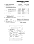
SECURITY DEVICE
102
/' 8O
,10O
,24
s
PEI/l A
f 12|SABUS
—$00t00:t:0;" _;g;
—
AEN
_
IOWW/
SUPEHl/U
r122
112
REAL TIME CLDCK [RTCl
|RD— PLUG/1ND
CH£JWElS__
114 CMDS
11
/118
POWER MANAGEMENT
120
IREGISTERS
(LOGICAL DEVICEZ)
(LUGICM. UEVIDE4)
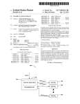
U.S. Patent
300
Oct. 9, 2001
\
US 6,301,665 B1
Sheet 3 6f 10
|
|
|
|
61h
LOGICAL DEVICE BASE ADDRESS LSB
60h
LOGICAL DEVICE BASE ADDRESS MSB
22h
SUPER IIO CONFIGURATION REGISTER
07h
LOGICAL DEVICE NUMBER
/ /|\ \
|
|
/
I, /
/
//
BASE
ADDRESS
_
|
g
\\
I
l
DATA
INDEX
/\
/
\
PASSWORD
PASSWORD
RTC 112
PM 118
FIG. 3
|
|
\_
\
\
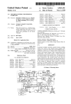
U.S. Patent
0a. 9, 2001
Sheet 4 0f 10
400
f 402
SUPER IIO CHIP FORCED TO
FIXED ADDRESS; PROGRAM
BASE ADDRESSES FOR
LOGICAL DEVICE NUMBERS
OF RTC 112 AND PM 118
UNPRDTECTED
OPERATION
WRITE TO INDEX
22h
?
412
PENDING
ACCESS TO INDEX
REGISTER 07h OF
SUPE?R IIO
FIG. 4A
US 6,301,665 B1
U.S. Patent
0a. 9, 2001
Sheet 5 0f 10
US 6,301,665 B1
424
LATCH WRITE
TO SUPER IIO
DATA REGISTER
PERMIT WRITE
TO DATA
REGISTER
420
CURRENT
CURRENT
LOGICAL DEVICE =
LOGICAL DEVICE =
LOGICAL DEVICE
NUMBER OF
LOGICAL DEVICE
NUMBER OF PM
RTC
LOGIC
f 422
BLOCK ACCESS TO
BLOCK ACCESS TO
INDEXES 60hl61h;
INDEXES GOhIGIh;
BLOCK ACCESSES TO
BLOCK ACCESSES TO
SPECIFIED RANGES 0F
RTC INDEXED
SPECIFIED RANGE(SI OF
POWER MANAGEMENT
REGISTER SPACE
IDDIIégLEgéSTEII
FIG. 4B
U.S. Patent
0a. 9, 2001
to
00
u)
vmm
:NE28E25;:
N6EZC5MB
Sheet 10 0f 10
mum
wzélsioE25
US 6,301,665 B1
O
O)
L!)
U52,_.%;>§H8 EIQ W EJIQP xézisl?wgu aml?éwozF
52@ a28
$@258a:
:N5w92a,:s
N2xézr%w?a 5@w2a8s3
mm.QI
US 6,301,665 B1
1
2
SECURITY METHODOLOGY FOR DEVICES
HAVING PLUG AND PLAY CAPABILITIES
slot is then placed in a “protected” state by issuing a
PROTECT RESOURCES command to the security device.
While in the locked state, a lock signal is asserted, Which
BACKGROUND OF THE INVENTION
secures system resources. To unlock the slot, the user issues
an ACCESS RESOURCE command to the security device,
1. Field of the Invention
folloWed by entry of the correct passWord. Correctly enter
This invention relates to security and personal computer
ing a slot’s passWord changes the state of the slot to
systems, and more particularly to a method for extending
“unprotected.” The security device passWord may only be
computer security features to devices having Plug and Play
Written if the slot is in the unprotected state. The security
device can only verify and does not divulge the passWord,
capabilities.
10
2. Description of the Related Art
The prevention of data theft is extremely important in
computer systems designed to exist on corporate netWorks
as Well as home computers. Companies and individuals
spend large sums of time and money developing data that
resides in these systems. Adequately protecting a computer
15
system’s resources from unauthoriZed access is thus a pri
upgrade or expand the capabilities of their computer systems
rather than buying an entirely neW system. In the past,
installing neW hardWare Was frequently a time-consuming
and frustrating process, requiring the computer user to
become familiar With architectural components such as
To address various security issues, including protection of
system ROM and other memory locations, a security device
Was developed as described in commonly-assigned US.
patent application Ser. No. 081779,061, entitled “SECU
RITY CONTROL FOR PERSONAL COMPUTE,” Which is
hereby incorporated by reference for all purposes as if set
25
provides a secure method for access to different system
resources, and Was capable of preventing data transfer via
externally accessible channels by turning off common sys
tem devices such as the parallel port, the serial port(s), the
?oppy disk controller, etc. The logic for all of these devices
dilemmas by creating the so-called Plug and Play (PnP)
speci?cation. Plug and Play is the industry term for the
technology that alloWs a computer system to understand a
user’s intentions to install option cards, for example, a sound
computer system’s “Super I/O” chip or similar device. The
Super I/O chip provides a mechanism to disable the various
card, into the computer system and automatically con?gure
it. This alloWs neW options to Work immediately folloWing
logical devices via one or more con?guration registers.
35
automatically ?gures the computer system’s bus and sets
key technology parameters for Plug and Play-ready add-in
unauthoriZed user. In current systems, security logic is used
to block ISA bus read and/or Write cycles to the registers in
cards. Previously, users had to set these parameters
manually, a complex and problematic exercise. When com
bined With features in certain operating systems, such as
the Super 1/ O chip responsible for turning system devices on
or off. The ISA cycles are blocked by gating an address
address for the Super I/O chip and the user has set What
installation Without disrupting existing system components.
When a neW option card is installed, Plug and Play ?rmWare
?cient protection. To make a system more secure, it is
necessary that the devices cannot be turned back on by an
enable signal AEN and/or I/O Write control IOWC# signal of
the Super I/O chip. UnauthoriZed cycles to the Super I/O
chip are blocked When the security logic decodes and I/O
direct memory access (DMA) and various system interrupts
(IRQs). Manipulation of various parameters Was often
required in order to ensure that its neWly added components
did not con?ict With existing components.
Against this backdrop, a number of hardWare and soft
Ware manufacturers undertook an initiative to solve these
as Well as other logical devices normally exists Within a
Merely turning off system devices, hoWever, is not suf
rapid pace.
For example, the oWners of today’s personal computers
(PCs) are faced With a myriad of options When choosing
peripheral devices. Frequently, computer users decide to
mary concern of computer users.
forth in its entirety. The security device described therein
thereby enhancing the security of the system. Providing
computer security is not a static process, hoWever, as tech
nology and neW threats to security continue to develop at a
WindoWs 95, Plug and Play greatly simpli?es the process of
setting up a personal computer system.
FolloWing the boot process, an operating system incor
45
porating Plug and Play support retrieves Plug and Play
information gathered by the BIOS. System resources are
amounts to a blocking enable bit.
then allocated amongst the Plug and Play cards. Con?ict
In prior systems, security logic in the security device
free resources for all inactive logical devices are also allo
protected certain ranges of non-volatile CMOS RAM Within
cated. All logical devices that have been con?gured are
activated, and device drivers are loaded. Details of Plug and
Play con?guration are generally knoWn or available to those
the Real-Time Clock (RTC) in the Super I/O chip. The
protected locations are used to store passWords and other
critical information. For example, assume that the I/O Index
register address of the RTC is 0070h and the address of the
Was in a predetermined range of indices to be protected.
skilled in the art Adding Plug and Play capabilities to the
Super I/O chip may create additional security concerns.
Speci?cally, the ISA Plug and Play architecture alloWs a
given chip to contain several “logical devices.” It does this
by alloWing each logical device to have its oWn base
address. The given chip decodes all addresses for its logical
Reads and Writes Would be blocked by holding the I/O Write
devices.
control signal IOWC# or address enable signal AEN to a
logic high level When the value of 0070h (the Index register
When the RTC located Within the Super 1/ O chip becomes
a Plug and Play logical device Whose base address can
address) Was in the range of an Index containing sensitive
information.
change, prior security devices may not adequately protect
Data register is 0071b. The prior security logic Would Work
by blocking reads or Writes to address 0071h When the
55
Index, tracked by examining Writes to the address 0071h,
the contents of the RTC. For example, an unauthoriZed user
The security device operates by providing multiple hard
could conceivably modify the base address of the RTC, and
Ware “lock” signals capable of being toggled by the user.
The lock signals restrict access to speci?c system resources
When asserted. In general, a user enters a passWord for a
particular memory “slot” in the security device. The memory
65
then gain access to unprotected Indexed locations. Other
logical devices of the Super I/O chip, such as poWer man
agement logic, may also have base I/O addresses capable of
being modi?ed. Further, the base address of the Super I/O
US 6,301,665 B1
3
4
chip itself may be modi?ed in an attempt to circumvent
security measures.
disable all of the data transfer devices in the Super I/O chip.
These devices include a ?oppy controller, a parallel port,
serial ports, and an infra-red port. This register is protected
SUMMARY OF THE INVENTION
to prevent an unauthoriZed user from enabling a previously
disabled data transfer device.
Brie?y, the present invention provides a security meth
odology and security logic for protecting certain Plug and
Play computer system components from unauthoriZed
Thus, the present invention permits system security mea
sures to be extended to devices incorporating features such
as Plug and Play compatibility.
access. The security logic utiliZes address enable and read/
Write control signals to the Super I/O chip to prevent access
to speci?c index registers corresponding to speci?ed logical
10
devices. The security logic also protects the base addresses
A better understanding of the present invention can be
of the Super I/O chip as Well as the base addresses of
obtained When the folloWing detailed description of the
preferred embodiment is considered in conjunction With the
speci?ed logical devices. Protecting the base addresses
prevents the security logic from being circumvented by
interfering With the address decoding used to track reads and
Writes to protected index registers.
In order to protect the base address of the Super I/O chip,
a speci?c index register in the index register set of the Super
I/O chip is monitored. FolloWing a Plug-and-Play boot
process, this index register, Which governs the base address
of the Super I/O chip, may be changed. In order to prevent
BRIEF DESCRIPTION OF THE DRAWINGS
15
folloWing draWings, in Which:
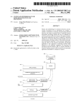
FIG. 1 is a block diagram of a computer system incor
porating security features in accordance With the present
invention;
FIG. 2 is a block diagram detailing speci?c portions of the
computer system of FIG. 1;
FIG. 3 is a diagram of various index register sets of a
this, security logic in accordance With the invention provides
Super I/O chip;
the option to block Write cycles to this index register. Such
blocking prevents a user from changing the base address of
methodology according to the present invention; and
the Super I/O chip.
FIGS. 4A and 4B are ?oWchart diagrams of a security
25
FIGS. 5A—5E are schematic diagrams of security logic for
providing security functions in accordance With the present
Next, With the base address of the Super I/O chip secured,
the base addresses of logical devices of interest arc secured.
In the Super I/O chip, the base address of a logical device is
changed by selecting a logical device number via a Super
I/O index (e.g., 07h), and then programming a 16 bit ISAbus
base address into additional indexes (e.g., 60/61h). To pre
vent such an occurrence, security logic according to the
invention monitors the current Super I/O chip index by
invention.
30
Commonly-assigned US. patent application Ser. No.
09/070,458, entitled “METHOD AND APPARATUS FOR
PROVIDING REMOTE ACCESS TO SECURITY FEA
TURES ON A COMPUTER NETWORK”, is hereby incor
porated by reference as if set forth in its entirety.
decoding the Super I/O chip’s base address (Index register).
When 07h is in the Index register, the security logic latches
Writes to the Super I/O chip’s corresponding Data register.
Computer System OvervieW
In the disclosed embodiment of the invention, the Real Time
Clock (RTC) and the PoWer Management logic of the Super
I/O chip comprise tWo protected logical devices If the
current logical device number matches either the logical
DETAILED DESCRIPTION OF INVENTION
40
Turning ?rst to FIG. 1, a typical computer system S
implemented according to the invention is illustrated. While
this system is illustrative of one embodiment of the
invention, the techniques according to the invention can be
implemented in a Wide variety of systems. The computer
device number of the RTC or the PoWer Management,
accesses to indexes 60/61h are blocked, thus protecting the
base addresses of these logical devices. The logical device
system S in the illustrated embodiment is a PCI bus/ISA bus
number of the RTC and the PoWer Management Block are
based machine, having a peripheral component interconnect
(PCI) bus 10 and an industry standard architecture (ISA) bus
12. The PCI bus 10 is controlled by PCI controller circuitry
located Within a memory/accelerated graphics port (AGP)/
PCI controller 14. This controller 14 (the “host bridge”)
programmable in the register space of the security logic.
In addition to protection of base addresses, the security
logic according to the present invention also alloWs for
protection of individual indexes for each of the protected
logical devices. The Super I/O chip provides a separate
index register set for operation of each of the logical devices.
45
50
Protection of individual indexes Within these additional
A second bridge circuit, a PCI/ISA bridge 24 (the “ISA
bridge”) bridges betWeen the PCI bus 10 and the ISA bus 12.
index register sets alloWs for speci?c functionality Within
each logic device to be protected.
For example, the nonvolatile RAM located in the RTC is
couples the PCI bus 10 to a processor socket 16 via a host
bus, an AGP connector 18 and a memory subsystem 20.
The host bridge 14 in the disclosed embodiment is a
55
252LX Integrated Circuit by Intel Corporation, also knoWn
used for system passWord storage. The security logic pro
vides programmable registers to designate ranges of the
PIIX4, also by Intel Corporation. The host bridge 14 and ISA
RTC index register space as protected ranges. These ranges
bridge 24 provide capabilities other than bridging betWeen
as the PCI AGP Controller (PAC). The ISA bridge 24 is a
may be used to store passWords such as an administrator
passWord and a poWer-on passWord. When programmed
With a base address of the RTC (alloWing for tracking of
indexes as described above), the security logic prevents
60
the memory subsystem 20. The ISA bridge 24 further
includes an internal enhanced IDE controller for controlling
up to four enhanced IDE drives 26, and a universal serial bus
accesses to these indexes When enabled.
Likewise, the security logic also provides the ability to
protect indexes in the PoWer Management logical device.
One of the PoWer Management indexes contains a function
enable register. This register alloWs the user to enable/
the processor socket 16 and the PCI bus 10, and the PCI bus
10 and the ISA bus 12. Speci?cally, the disclosed ISA bridge
14 includes interface circuitry for the AGP connector 18 and
65
(USB) controller for controlling USB ports 28.
The host bridge 14 is preferably coupled to the processor
socket 16, Which is preferably designed to receive a Pentium
US 6,301,665 B1
5
6
II processor module 30, Which in turn includes a micropro
cessor 32, as Well as an additional code for execution by
cessor core 32 and a level tWo (L2) cache 34. The processor
microcontrollers in a ROM-sharing arrangement.
The ISA bus 12 further couples the ISA bridge 24 to a
socket 16 could be replaced With processors other than the
Pentium II Without detracting from the spirit of the inven
tion.
security, poWer, ACPI, and miscellaneous application spe
ci?c integrated circuit (ASIC) 80, Which provides a variety
The host bridge 14, When the Intel 440LX North Bridge
is employed, supports extended data out (EDO) dynamic
of miscellaneous functions for the system as set forth in
random access memory (DRAM and synchronous DRAM
(SDRAM), a 64/72-bit data path memory, a maximum
memory capacity of one gigabyte, dual inline memory
module (DIMM), serial presence detect, eight roW address
and security logic (FIG. 2) according to the present
invention, system poWer control, light emitting diode (LED)
greater detail beloW. The ASIC 80 includes security features
10
control, hood lock control, ACPI registers and support,
system temperature control, and various glue logic. Finally,
strobe (RAS) lines, error correcting code ECC) With single
and multiple bit error detection, read-around-Write With host
for PCI reads, and 3.3 volt DRAMs. The host bridge 14
support up to 66 megahertZ DRAMs, Whereas the processor
socket 16 can support various integral and non-integral
a video display 82 can be coupled to the AGP connector 18
for display of data by the computer system S.
15
multiples of that speed.
Again, a Wide variety of systems could be used instead of
the disclosed system S Without departing from the spirit of
the invention.
Referring noW to FIG. 2, a block diagram detailing
The ISA bridge 24 also includes enhanced poWer man
agement. It supports a PCI bus at 30 or 33 megahertZ and an
ISA bus 12 at 1A1 of the PCI bus frequency. PCI revision 2.1
is supported With both positive and subtractive decode. The
standard personal computer input/output (I/O) functions are
supported, including a dynamic memory access (DMA)
controller, tWo 82C59 interrupt controllers, an 8254 timer, a
real time clock (RTC) With a 256 byte complementary metal
oxide semiconductor (CMOS) static RAM (SRAM), and
control, a PCI arbiter, remote Wake up logic, system ?n
speci?c portions of the computer system S of FIG. 1 is
provided. The ASIC 80 contains a security device 100 for
securely maintaining various passWords (in the slots 102),
25
although the security device 100 could be implemented in
other system components. The preferred embodiment of the
security device 100 comprises the folloWing elements: a
keyboard controller, an external microcontroller, and tWo
general purpose devices. The enhanced poWer management
Within the ISA bridge 24 includes ?ll clock control, device
plurality of memory slots 102 to store passWords for pro
tected resources; a command register 106 for the security
device 100; and a status/data register 104 for communicating
With the computer system S. These components alloW a user
key information to be compared to the passWords stored in
the memory slots.
management, suspend and resume logic, advanced con?gu
ration and poWer interface (ACPI), and system management
internal to the security device 100, or by other related or
chip selects for system read only memory (ROM), RTC,
bus (SMBus) control, Which implement the inter-integrated
circuit (I2C) protocol.
The PCI bus 10 couples a variety of devices that generally
take advantage of a high speed data path. This includes a
The comparison process may be carried out by logic
closely coupled logic such as security logic 108. The precise
35
con?guration of the logic used in the comparison process is
not considered critical to the invention. HoWever, the con
tents of the memory slots 102 should not be ascertainable
small computer system interface (SCSI) controller 26, With
during the comparison process. Exemplary operation of the
both an internal port 38 and an external port 40. In the
disclosed embodiment, the SCSI controller 26 is a AIC-7860
SCSI controller. Also coupled to the PCI bus 10 is a netWork
security logic 108 and protection of the memory slots is
described in the previously-incorporated US. Patent Appli
cation entitled “METHOD AND APPARATUS FOR PRO
VIDING REMOTE ACCESS TO SECURITY FEATURES
ON A COMPUTER NETWORK”.
interface controller (NIC) 42, Which preferably supports the
ThunderLanTM poWer management speci?cation by Texas
Instruments. The NIC 42 is coupled through a physical layer
44 and a ?lter 46 to an RJ-45 jack 48, and through a ?lter
50 to aAUI jack 52. The NIC 42 alloWs information such as
45
The Super I/O chip 62 supports ISA Plug-and-Play func
tionality as indicated by Plug-and-Play (PnP) 122 in FIG. 2,
passWords and other data to be received and provided by the
computer system S.
and contains several logical devices. In the disclosed
embodiment of the invention, the logical devices of interest
for security purposes include the Real Time Clock (RTC)
BetWeen the PCI Bus 10 and the ISA Bus 12, an ISA/PCI
backplane 54 is provided Which include a number of PCI and
112 (logical device 2), and PoWer Management (PM) logic
ISA slots. This alloWs ISA cards or PCI cards to be installed
memory 114 locations Where the poWer-on passWord and the
administrator passWord of the disclosed embodiment of the
invention are stored for provision to the slots 102 during
118 (logical device 8). The RTC 112 contains CMOS
into the system for added functionality.
Further coupled to the ISA Bus 12 is an enhanced sound
system chip (ESS) 56, Which provides sound management
through an audio in port 58 and an audio out port 60. The
ISA bus 12 also couples the ISA bridge 24 to a Super I/O
chip 62, Which in the disclosed embodiment is a National
poWer-up. The contents of the RTC 112 are maintained
55
Semiconductor Corporation PC87307VUL device. This
Super I/O chip 62 provides a variety of input/output
functionality, including a parallel port 64, an infrared port
66, a keyboard controller for a keyboard 68, a mouse port for
a mouse port 70, additional series ports 72, and a ?oppy disk
drive controller for a ?oppy disk drive 74. These devices are
coupled through connectors to the Super I/O 62.
The ISA bus 12 is also coupled through bus transceivers
76 to a Flash ROM 78, Which can include both basic
input/output system (BIOS) code for execution by the pro
during poWer-doWn by an external battery. Access to these
passWord locations is restricted to prevent the unauthoriZed
reading or changing of a passWord. The PM logic 118
contains a Function Enable register 120 used to enable/
disable several system hardWare resources (devices) located
Within the Super I/O chip 62. These devices include the
parallel port 64, the tWo serial ports 22, and other resources.
The ASIC 80 of the disclosed embodiment of the inven
tion is capable of preventing read and/or Write accesses to
various registers of the Super I/O chip 62 by controlling the
65
address enable input signal AEN and the I/O Write control
input signal IOWC# to the Super I/O chip 62. More
speci?cally, security logic 108 Within the ASIC 80 drives the
US 6,301,665 B1
8
7
address enable input signal AEN and the input/output Write
control input signal IOWC# of the Super I/O chip 62. In the
disclosed embodiment of the invention, the Super I/O
address enable signal SIOAEN and the Super I/O Write
control signal SIOWCL are selectively asserted by security
logic 108 of the ASIC 80 to prevent the Super I/O chip 62
from decoding read and/or Write cycles to the protected
locations and select registers Within the Super I/ O chip 62 as
As noted above, the Super I/O chip 62 of the disclosed
embodiment of the invention incorporates numerous
features, including Plug-and-Play capabilities 122. The
Super I/O chip 62 utiliZes an indexed addressing scheme,
involving an Index and Data register pair, for its internal
con?guration registers. The initial I/O port locations of the
Index and Data register pair are determined by hardWare
strapping at reset, and are set for 015Ch and 015Dh,
set forth beloW.
In general, When the ASIC 80 detects an I/O read or I/O
may block the cycle With programmed security options.
respectively, in the disclosed embodiment of the invention,
With full 16-bit decoding. The base addresses of the Index
and Data register pair may be changed in softWare after reset
Speci?cally, if access to the particular Super I/O chip 62
resource being addressed has been locked, the current cycle
Will be blocked and not seen by the Super I/O chip 62.
Control of the security logic 108 is described in greater
through a 16-bit programmable register (see FIG. 3). The
hardWare strapping also indicates that the Super I/O chip 62
is in Plug and Play motherboard mode. The con?guration
registers are accessed by Writing the appropriate logical
Write cycle address to the Super I/O chip 62, the ASIC 80
15
detail beloW.
Due to the ISA Plug-and-Play capabilities 122 of the
Super I/O chip 62, its base I/O address is programmable, as
device number at Index 07h, folloWed by Writing the desired
offset value to the Index register, and then reading or Writing
to the Data register.
are the base 1,0 addresses of its logical devices. Several
registers must therefore be secured to insure that the appro
priate resources are protected. In the disclosed embodiment
of the invention, these registers are secured through the use
Asic 80 Security Registers 110
of Super I/O security registers 110 in the ASIC 80, as Well
as the aforementioned signal routing to the Super I/O chip 62
on the system board.
25
This section describes in a tabular manner the Super I/O
By using the security device 100 in conjunction With the
security registers 116 of the Super I/O chip 62, a poWer-on
passWord is protected by storing the current poWer-on pass
security registers 110 included in the ASIC 80 to implement
the security mechanism described herein.
Word in slot “1” of the slots 102 and issuing a PROTECT
RESOURCES command. Once slot 1 is loaded With a
passWord and the PROTECT RESOURCES command is
executed, it is not possible to read or Write the poWer-on
passWord at its pre-programmed location in the CMOS
memory 114 of the Super I/O chip 62.
If slot 1 of the security device 100 has been placed in the
ASIC 80 Security Register Summary
System Management Registers
35
PROTECT RESOURCES or PERMANENT LOCK state,
and the last data Write to the RTC 112 index register
address enable signal SIOAEN is forced high for any read or
RTC 112. This functions to prevent the Super I/O chip 62
from responding to reads and Writes to and from the poWer
on passWord storage area. When blocking all Writes, the
45
asserted by the security logic 108, protects the Flash ROM
78 from unauthoriZed Write operations. The Flash ROM
Write protect signal FRWPL can only be asserted to protect
the Flash ROM 78 if a passWord is stored in slot “0” of the
Super I/O chip 62 security registers 110. Further details of
the operation of the administrator passWord as disclosed in
the previously-incorporated US. patent application entitled
Address
OC5O
Index
80h
81h
82h
83h
OC51
OC51
Write cycles directed to the data register (not shoWn) of the
slots 102 folloWed by a PROTECT RESOURCES or PER
MANENTLY LOCK RESOURCES command for slot 0.
The Flash ROM Write protect signal FRWPL is not asserted
folloWing a hardWare reset.
In the disclosed embodiment of the invention, the admin
istrator passWord contained in slot 2 can be utiliZed to secure
a variety of system resources, including: a hood lock register
used to prevent unauthoriZed opening of the chassis of the
computer system S, a secure GPIO register, and the various
R/W
R/W
R/W
OC51
OC51
OC51
corresponds to the poWer-on passWord range, the Super I/O
Super I/O Write control signal SIOWC is manipulated in a
similar fashion to the Super I/O address enable signal
SIOAEN for blocking reads and Writes.
The Flash ROM Write protect signal FRWPL, When
Address
OC5O
OC51
55
Description
Index Register
Data Register
SIO Base Address MSB
SIO Base Address LSB
SIO Current Index Value
84h
SIO Current Logical Device
SIO Blocking Control
OC51
OC51
85h
86h
SIO Blocked Index Value 0
SIO Blocked Index Value 1
OC51
OC51
8Fh
90h
Base Address Blocking Control
PM Logical Device
OC51
OC51
OC51
91h
92h
93h
PM Base Address MSB
PM Base Address LSB
PM Current Index
OC51
94h
PM Blocking Control
OC51
OC51
95h
96h
PM Blocked Index 0
PM Blocked Index 1
OC51
AOh
CMOS Logical Device
OC51
OC51
OC51
A1h
A2h
A3h
CMOS Base Addr MSB
CMOS Base Addr LSB
CMOS Current Index
OC51
A4h
CMOS Blocking Control
OC51
A5h
CMOS PoPW LoW Index
OC51
A6h
CMOS PoPW High Index
OC51
A7h
CMOS AdmPW LoW Index
OC51
OC51
A8h
COh
CMOS AdmPW High Index
Security Control
SUPER I/O BASE ADDRESS MSB: The base address of
the Super I/O chip 62 is stored across tWo registers. The
most signi?cant byte of the address is stored in this 10
“METHOD AND APPARATUS FOR PROVIDING 65 register. The least signi?cant byte is stored in the Super I/O
REMOTE ACCESS TO SECURITY FEATURES ON A
Base Address LSB register. The Super I/O Base Address
COMPUTER NETWORK”.
must be aligned to a Word (2 byte) boundary.
US 6,301,665 B1
9
10
-continued
Bit
Description
[7:0]
Bit
Most Signi?cant Byte of the Super I/O Base Address Register.
This byte represents bits [15:8] of the Super I/O Base
5
Address register.
Description
SUPER I/O BASE ADDRESS BLOCKING CONTROL:
[7]
[6]
Reserved. Return 0 on read.
Reads/Writes to CMOS Base Address. When this bit is set to
a ‘1,’ ASIC 80 Will block both reads and Writes to the
Super I/O Data register When/if the Current IndeX value is
_
_
10
60h or 61h, and the Current Logical device register rnatches
SUPER I/O BASE ADDRESS LSB: The least slgnl?cant
byte of the address is stored in this register. The most
the CMOS Logical Device Number register. This Will prevent
changes to the CMOS Base Address.
Signi?cant byte is Stored in the Super I/O Base Address MSB
[5]
register
'
Bit
Description
[7:1]
Least Signi?cant Byte of the Super I/O Base Address Register.
This byte represents bits [7:1] of the Super I/O Base Address
register.
[4]
[7:0]
20
Reserved. Return 0 on read.
SUPER I/O CURRENT INDEX:
Current Value of the Super I/O IndeX register. This value is used
for comparison With the Super I/O Block IndeX values. If blocking
is enabled, When this value matches a Super I/O Blocked IndeX
Value reads and/or Writes to the Super I/O Data register are be
blocked.
[3]
[2]
25
[1]
SUPER I/O CURRENT LOGICAL DEVICE:
[7:0]
device register matches the PM Logical Device Nurnber
register. This Will prevent changes to the Power Management
Base Address
Block Reads/Writes to Super I/O Base Address. When this bit
is set to a ‘1,’ ASIC 80 Will block both reads and
Writes to the Super I/O Data register When/if the Current
IndeX value is 22h. This Will prevent changes to the Super
I/O Base Address.
Reserved. Return 0 on read.
Block Reads/Writes to CMOS Base Address. When this bit is set
to a ASIC 80 Will block Writes to the Super I/O Data register
When/if the Current IndeX value is 60h or 61h, and the Current
Logical device register matches the CMOS Logical Device Nurnber
register. This Will prevent changes to the CMOS Base Address.
Block Reads/Writes to Power Management Base Address. When
this bit is set to a ‘1,’ ASIC 80 Will block Writes to the
Current Logical Device. This byte holds the logical device being
addressed in the Super I/O chip 62. This value is used to determine 30
When the Power Management logical device 118 or the CMOS
logical device (RTC 112) is being addressed. If this value matches
[0]
the logical device number for Power Management logical device
118 or RTC 112, Writes to Super I/O Indexes 60h, and 61h Will be
blocked. This Will prevent a change to the I/O base address
of the current logical device.
SUPER I/O INDEX BLOCKING CONTROL:
I
both reads and Writes to the Super I/O Data register When/if
the Current IndeX value is 60h or 61h, and the Current Logical
15
0
Block Reads/Writes to the Power Management Base Address.
When this bit is set to a ‘1,’ ASIC 80 Will block
35
Super I/O Data register When/if the Current IndeX value is
60h or 61h, and the Current Logical device register
matches the PM Logical Device Nurnber register. This Will
prevent changes to the Power Management Base Address.
Block Read/Writes to Super I/O Base Address. When this bit
is set to a ‘1,’ ASIC 80 Will block Writes to the
Super I/O Data register When/if the Current Index value is
22h. This Will prevent changes to the Super I/O Base Address.
POWER MANAGEMENT LOGICAL DEVICE NUMBER:
[7:0] Power Management Logical Device Number. This register
[7:6]
[5]
[4]
[3:2]
[1]
Reserved. Return 0 on read.
Block Reads/Writes frorn SIO Blocked IndeX 1. When this bit is
set to a ‘1,’ the ASIC 80 Will block both reads and
Writes to the Super I/O Data register if the Current Index
value rnatches SIO Blocked IndeX 1.
Block Reads/Writes frorn SIO Blocked IndeX 0. When this bit is
set to a ‘1,’ the ASIC 80 Will block both reads and Writes to
is prograrned With the value of the Power Management logical
40
the Super I/O Data register if the Current IndeX value rnatches
SIO Blocked Index 0'
Reserved. Return 0 on read.
Block Writes frorn SIO Blocked IndeX 1. When this bit is set to
base address of the Power Management logical device 118
is stored across two registers. The most signi?cant byte of
.
.
.
.
.
.
45 [he addres_s 1S Stored 1n thls reglster' The least slgnl?cant byte
device nurnber. Having this value alloWs ASIC 80 to block
accesses (and therefore changes) to the Base Address of the
POWER MANAGEMENT BASE ADDRESS MSBZ The
a ‘1; the ASIC 80 will block Writes to the Super {/0 Data
[0]
15 stored in the Super I/O Base Address LSB register. The
register if the Current IndeX value rnatches SIO Blocked IndeX 1.
Super I/O Base Address must be aligned to a Word (2 byte)
Block Writes from the SIO Blocked IndeX 0. When this bit is set to
a ‘1,’ the ASIC 80 Will block Writes to the Super I/O Data
register if the Current IndeX value rnatches SIO Blocked IndeX 0.
boundary
SUPER I/O BLOCKED INDEX VALUE 0:
[7:0]
Power Management logical device 118.
50
Super I/O Blocked IndeX Value 0. This value deterrnines an IndeX
Bit Description
of the Super I/O register space to Which accesses can be blocked
_
by ASIC 80. This IndeX is compared With the value of the Super
I/O Current IndeX register to determine Whether a read or Write
to a potentially blocked IndeX is occurring. If this register
_
[7:0] MOS} slgm?Fant Byte of the Power Management Base Address
Reglster' Thls byte represents bl_ts [15:8] of the Power
Management Base Address Reglster'
55
matches the Current IndeX value, and a read or Write occurs to
the Super I/O Data register, ASIC 80 Will block the access if
enabled via the Super I/O Blocked IndeX Control Register.
[7:0]
SUPER I/O BLOCKED INDEX VALUE 1:
_
_
Super I/O Blocked IndeX Value 1. This value deterrnines
an IndeX of the Super I/O register space to Which accesses can be
POWER MANAGEMENT BASE ADDRESS LSB: The
least signi?cant byte of the address is stored in this register.
The most signi?cant byte is stored in the Super I/O Base
Address MSB register.
blocked by ASIC 80. This IndeX is compared With the value of the
Super I/O Current IndeX register to determine Whether a read
or Write to a potentially blocked IndeX is occurring.
If this register matches the Current IndeX value, and a read
or Write occurs to the Super I/O Data register, ASIC 80 Will
block the access if enabled via the Super I/O Blocked IndeX
Control Register.
Bit
Description
[7:1] Least Signi?cant Byte of the Power Management Base
Address Register. This byte represents bits [7:1) of the
US 6,301,665 B1
11
12
-continued
Bit
Description
Bit
0
Reserved. Return 0 on read.
POWER MANAGEMENT CURRENT INDEX:
[7:0]
Current Value of the PoWer Management IndeX register. This
value is used for comparison With the PoWer Management Blocked
IndeX values. If blocking is enabled, When this value matches
a PoWer Management Blocked IndeX Value reads and/or Writes to
the PoWer Management Data register Will be blocked.
POWER MANAGEMENT INDEX BLOCKING CONTROL:
Power Management Base Address register.
5
Description
[7:1]
0
[7:6]
[5]
Reserved. Return 0 on read.
CMOS CURRENT INDEX:
10 [7:0]
Reserved. Return 0 on read.
Block Reads/Writes from PM Blocked IndeX 1. When this bit is set 15
to a ‘1’ ASIC 80 Will block both reads and Writes to the PM
[7:6]
data register if the PM Current IndeX value matches the PM
[5]
data register if the PM Current IndeX value matches the PM
[3:2]
[1]
[0]
Current Value of the CMOS IndeX Register. This value is used for
comparison With the CMOS Blocked PassWord Ranges. If blocking
is enabled, When the value falls Within a Blocked PassWord
Range, reads and/or Writes to the CMOS Data Register Will
be blocked.
CMOS INDEX BLOCKING CONTROL:
Reserved. Return 0 to read.
Reads/Writes from CMOS Administrator PassWord IndeX Range.
Blocked IndeX 1.
Block Reads/Writes from PM Blocked Index 0. When this bit is set
to a ‘1’ ASIC 80 Will block both reads and Writes to the PM
[4]
Least Signi?cant Byte of the CMOS Base Address Register.
This byte represents bits [7:1] of the CMOS Base Address
Register.
When this bit is set to a ‘1,’ ASIC 80 Will block both reads and
Writes to the CMOS data register if the CMOS Current IndeX value
falls Within the Administrator PassWord Range.
20 [4]
Block Reads/Writes from CMOS Blocked IndeX 1. When this bit is
Blocked Index 0.
set to a ‘1,’ ASIC 80 Will block both reads and Writes to the
Reserved. Return 0 on read.
Block Writes from PM Blocked IndeX 1. When this bit is set to a
‘1’ ASIC 80 Will block Writes to the PM data register if the
PM Current IndeX value matches PM Blocked IndeX 1.
Block Writes from PM Blocked Index 0. When this bit is set to
a ‘1’ ASIC 80 Will block Writes to the PM data register if
the PM Current IndeX value matches PM Blocked Index 0.
POWER MANAGEMENT BLOCKED INDEX 0:
CMOS data register if the CMOS Current IndeX value falls Within
the PoWer-On PassWord Range.
Reserved. Return 0 on read.
Block Reads/Writes from CMOS Administrator PassWord Index
Range. When this bit is set to a ‘1,’ ASIC 80 Will
block Writes to the CMOS Data Register if the CMOS Current
IndeX value falls Within the Administrator PassWord Range.
Block Reads/Writes from CMOS Blocked IndeX 1. When this
[3:2]
[1]
25
[0]
bit is set to a ‘1,’ ASIC 80 Will block Writes to
[7:0]
PoWer Management Blocked IndeX Value 0. This value determines
the CMOS Data Register if the CMOS Current IndeX value falls
an IndeX of the PM register space to Which accesses can be
blocked
Within the PoWer-On PassWord Range.
cMOS POWER-ON PASSWORD LOW INDEX:
30
by ASIC 80. This IndeX is compared With the value of the PM
Current Index Register to determine Whether a read or Write to
a Potentially blocked Index is Occurrihg- If this register matches
the PM Current IhdeX Value and a read or Write Occurs
to the PM data register, ASIC 80 will block the access if enabled
Via the PM Blocked IhdeX Control Registeh
POWER MANAGEMENT BLOCKED INDEX 11
[7:0]
35
LoWer IndeX of the PoWer-On PassWord. This register holds
the lOW end of the range of indices used to store the PoWer-On
password. The upper end of the range is stored in the PoWer-On
Password High Index Register_ when CMOS Blocking Control
enables blocking of this range, the value of the CMOS Current
IndeX value is compared against this LoW-to-High range.
cMOS POWER-ON PASSWORD HIGH INDEX:
[7:0]
PoWer Management Blocked IndeX Value O. This value determines
ah Index of the PM register Space to Which accesses can he
blocked
_
_
[7:0]
_
Upper IndeX of the PoWer-On PassWord. This register holds
the high end of the range of indices used to store the PoWer-On
by ASIC 80. This Index is compared With the value of the PM
Current IndeX Register to determine Whether a read or Write to a
potentially blocked IndeX is occurring. If this-register matches
the PM _Chrreht IhdeX Vahle ahd a read or Whte eeehrs te the PM
40
password The lower end of the range is Stored in the
POWer_On LOW Index registen When CMOS Blocking Control
enables blocking of this range, the Value of the CMOS Current
IndeX value is compared against this LoW-to-High range. If the
data register, ASIC 80 Will block the access if enabled via the PM
Current Index fans Within the range, the Cycle to the CMOS
Blocked IndeX Control Register.
w
data register is blocked
cMOS ADMINISTRATOR PASSWORD LOW INDEX:
45
[7:0] CMOS Legteal Devtee Nuthheh Thte reglster 1S preghaththed Wtth
[7:0] LoWer IndeX of the Administrator PassWord. This register holds
the Value of the CMOS Legleal Devlee Nhthheh Havlhg thls Value
aheWS ASIC 80 to hleek aceesseS (ahd therefore ehahges) to the
Base Address of the CMOS devlee'
50
CMOS BASE ADDRESS MSBZ The base address of the
.
.
.
the lOW end of the range of indices used to store the Administrator
passWord. The upper end of the range is stored in the Administrator
PassWord High IndeX register. When CMOS Blocking control
enables blocking of this range, the value of the CMOS Current
IndeX value is compared against this LoW-to-High range. If the
Current ‘Index falls Within the range, the cycle to CMOS data
.
register is blocked.
RTC 112 is stored across tWO registers. The most signi?cant
CMOS ADMINISTRATOR PASSWORD HIGH INDEX:
byte of the address is stored in this register. The least
Signi?cant byte is Stored in the CMOS Base Address LSB
[7:0] Upper IndeX of the Administrator PassWord. This register holds
register' The CMOS Base Address must be aligned to a Word 55
the high end of the range of indices used to store the Administrator
passWord. The loWer end of the range is stored in the Administrator
(2 byte) boundary‘
PassWord LoW IndeX register. When CMOS Blocking Control
enables blocking of this range, the value of the CMOS Current
IndeX value is compared against this LoW-to-High range.
If the Current IndeX falls Within the range, the cycle to
Bit
[7:0]
Description
60
the CMOS data register is blocked.
Most Signi?cant Byte of the CMOS Base Address. This byte
represents bits [15:8] of the CMOS Base Address Register.
CMOS BASE ADDRESS LSB: The least signi?cant byte 65
of the address is stored in this register. The most signi?cant
byte is stored in the CMOS Base Address MSB register.
SECURITY CONTROLI T0 Wnte t0 thls reglster, slot 2
(AdIIliIliSIfaIOf PaSSWOfd) 0f the security device 100 must be
unlocked.
US 6,301,665 B1
14
13
base address of a logical device of the Super I/ O chip 62 may
be changed by selecting the logical device number via Index
Bit
Description
[7]
Full Proof Mode. This bit can be used to close a potential security
hold in the ASIC 80 security scheme. When set to a ‘1’ this bit will
07h, then programming the base address into indexes 60h
and 61h.
In addition to protection of base addresses, the security
logic 108 and security registers 110 according to the present
prevent an unlock of Slot 2 (Administrator Password) from
invention also allow for protection of individual indexes for
clearing the Security Lock bit (bit 0 of this register) if password
was NOT stored in Slot 2 at the time the Security Lock bit was set.
Under normal operation (Full Proof Mode = ‘0’), the act
of unlocking Slot 2 will clear the Security Lock bit. Clearing the
10
Security Lock bit equates to an unsecured system because
modi?cations can be made to the ASIC 80 security registers
and therefore to the Super I/O registers. With no password
in Slot 2, an unauthorized use could write a dummy password
in Slot 2, issue a Protect Resources command, then issue an
Access Resources command and unlock Slot 2.
This would clear the Security Lock bit and render
the system unsecured. Setting Full Proof Mode to ‘1’ will prevent
the clearing of Security Lock when there was not Slot 2 password
loaded, thereby allowing the system to stay secure. When set to
a ‘0’, this bit allows the Security Lock bit to function normally.
1 = Prevent unlock of Slot 2 from clearing Security Lock bit (bit
0 of this register) if a password was not stored in Stoic when the,
individual indexes within these additional index register sets
allows for speci?c functionality within each logic device to
be protected.
For example, the nonvolatile RAM located in the RTC
15
as an administrator password and a power-on password.
20
Security Lock bit was set.
enabled. Likewise, the security logic 108 also provides the
ability to protect indexes in the Power Management logical
Security Lock. This bit is used to lock ASIC 80’s security system.
Until this bit is set, all of the security related registers with
ASIC 80 can be modi?ed. The ability to modify these registers
leaves the Super I/O chip 62 unprotected. Setting this bit to
device 118.
Referring now to FIGS. 4A and 4B, ?owchart diagrams of
a ‘1’ will prevent all writes to the ASIC 80
an exemplary security methodology in accordance with the
security registers. In addition, the base addresses of the
Super I/O chip 62 and its logical devices will be protected
if their protection is enabled via the Base Address Blocking
30
the exception.
1 = ASIC 80 security is ON
0 = ASIC 80 security is OFF
When programmed with a base address of the RTC 112
(allowing for tracking of indexes as described above), the
security logic 108 prevents accesses to these indexes when
Reserved. Return 0 to read.
Control register. To secure the system, this bit must be set
to a ‘1’ by software. Normally, the bit is cleared when
Slot 2 of the security device 100 transitions from the locked
state to the unlocked state. See the description of
the Full Proof Mode bit for a more detailed description of
112 is used for system password storage. The security logic
provides programmable registers described above to desig
nate ranges of the RTC index register space as protected
ranges. These ranges may be used to store passwords such
0 = Security Lock bit (bit 0 of this register) functions normally.
[6:1]
[0]
each of the protected logical devices. As illustrated, the
Super I/O chip 62 provides a separate index register set for
operation of each of the logical devices. Protection of
35
present invention is shown. The methodology commences in
step 400 following reset of the computer system S. In step
402, a hardware strapping option on pins of the Super I/O
chip 62 de?nes an address for the Index and Data registers.
This prevents contention between the registers for I/O
address space. It should be noted that the base address is for
the Index and Data registers of the Super I/O chip 62 are
essentially the base address of the main index register set of
the Super I/O chip 62. Also in step 402, the base addresses
for logical device numbers for RTC 112 and the Power
An exemplary security methodology utilizing theses reg
ister is described below in conjunction with FIGS. 4A and
4B.
Referring now to FIG. 3, a diagram of various registers of
a Super I/O chip 62 utilized by the present invention is
shown. The main index register set 300 of the Super I/ O chip
Management logic 118 are programmed into the Super I/O
40
the security device 100 are set. In the disclosed embodiment
of invention, the slots 102 of the security device 100 are
utilized to enable access to the secured features of the Super
contains a number of indexes of interest in the disclosed
embodiment. Only two system I/O addresses are required to
access any of the con?guration registers. Speci?cally, an
Index and Data register pair 15 used to access registers for
all read and write operations.
45
In a write operation, the target con?guration register is
identi?ed, based on a value that is loaded into the Index
register. Then, the data to be written into the con?guration
register is transferred via the Data register. Similarly, for a
read operation, the source con?guration register is identi?ed,
based on a value that is loaded into the Index register. The
data to be read is then transferred via the Data register.
55
Reading the Index register returns the last value loaded into
the Index register. Reading the Data register returns the data
Super I/O con?guration register de?ning the base address of
Super I/O chip 62; and index register values 60h and 61h
reference the base address of a speci?ed logical device. The
I/O chip 62. If the security logic 108 is not enabled as
determined in step 404, control proceeds to step 406 and
operation of the computer system S proceeds in a manner
which allows for unprotected access to the con?guration
registers and other secured resources of the Super I/O chip
62.
If the security logic 108 is enabled is provided for in step
404, control passes to step 408 where pending writes to the
main index register set of the Super I/O chip 62 are exam
ined for a pending write to Index 22h, which is a Super I/O
chip 62 con?guration register that allows the base address of
the Super I/O chip to be modi?ed. If the pending write is to
Index 22h in the Super I/O chip register space, the pending
write cycle is blocked by the security logic 108 in step 44.
in the con?guration register pointed to by the Index register.
Further details of the operation of these registers can be
found in the speci?cation for the National Semiconductor
Corporation PC87307VUL device.
Of interest in the disclosed embodiment of the present
invention, the index register value 07h speci?es a logical
device number; the index register value 22h references a
security register 110 as described above.
Next, in step 404, the state of the security logic 108 and
60
Again, the base address of the Super I/O chip 62 as well as
the current Index value of the pending write is stored in the
security registers 110 as described above. The security logic
108 tracks the current Super I/O chip 62 Index by decoding
the Super I/O chip 62 base address (Index register).
If the pending write cycle to the Super I/O chip 62 is not
65
to Index 22h as determined in step 408, control proceeds to
step 412 where it is determined if the pending access is to
Super I/O chip 62 Index 07h (note that the precise ordering
US 6,301,665 B1
15
16
of steps 408 and 412 is not consider critical to the invention).
If 07h is not in the Index register as determined by the
unlock signal ADMiUNLOCKiand a blocking signal gen
erated by the logic of FIG. 5E. Thus, a number of conditions,
de?ned largely by the contents of the registers described
security logic 108 in step 412, control returns to step 404,
Which is also Where control proceeds following step 410.
above and the address on the data bus, may cause assertion
of the Super I/O address enable signal SIOAEN.
The Super I/O Write control signal SIOWCL is provided
by the output of a four input OR gate 510. One input of the
OR gate 510 is driven by an 10 Write control signal IOWC#
While the remaining inputs are driven by AND gates 512,
516, and 518. The Super I/O Write control signal SIOWCL
is asserted folloWing assertion of any of the inputs of the OR
If it is determined in step 412 that an access to Index
register 07h is pending, control proceeds to step 414 (FIG.
4B) Where the security logic 108 latches Writes to the Data
register of the Super I/O chip 62. Since the base address of
a logical device of the Super I/O chip 62 may be changed by
selecting the logical device number via Index 07h, then
programming the base address into Indexes 60—61h, protec
tion of these indexed locations is desirable When the base
address of a speci?ed logical device is to be protected.
Next, in step 416, it is determine Whether the current
logical device equals the programmable logical device num
gate 510. The output of AND gate 512 is asserted if bit Zero
of the Security Control Register is asserted, as Well as the
output of a three input OR gate 514. The inputs of the OR
15
ber of the RTC 112. If so, control proceeds to step 418 Where
unlock signal POPiUNLOCKias Well as a blocking signal
all accesses to Indexes 60—61h are blocked. In addition,
accesses to speci?ed ranges of the CMOS memory 114 of
generated by the logic of FIG. 5E. Similarly, the inputs of
AND gate 518 are driven by the administrator unlock signal
ADMiUNLOCK, as Well as a blocking signal generated by
the RTC 112 index register space are blocked. As noted
above, in the disclosed embodiment of the invention, pro
the logic of FIG. 5E. Thus, the Super I/O Write control signal
grammable registers designating ranges of index register
SIOWCL is also asserted under a variety of security states.
Referring noW to FIG. 5B, a blocking address enable
space of the RTC 112 to be protected are provided. These
ranges may be used, for example, to store the Administrator
PassWord and the PoWer-On PassWord. Thus, When pro
grammed With the base address of the RTC 112 (to permit
tracking of the Indexes as described above), the security
logic 108 prevents access to speci?ed ranges When enabled.
If the current logical device does not equal the logical
25
device number of the RTC 112 as determined in step 416,
control passes to step 420 to determine if the current logical
device equals the logical device number of the PoWer
Management logical device 118. If so, control passes to step
422, Where access is to Indexes 60—61h are blocked. In
addition, the disclosed security logic 108 also provides the
ability to protect tWo indexes in the PoWer Management
logical device 118. One of the protected PoWer Management
indexes contains a function enable register 120. This register
35
signal BLOCKiEANiBA used by the logic of FIG. 5A is
provided by the output of an AND gate 520. One input of the
AND gate 520 is driven by a Super I/O data register decode
signal SIOiDATiREG DEC FIG. 5C), While the other
input is provided by the output of a three input OR gate 522.
Inputs to the OR gate 522 include the outputs of AND gates
524, 526, and 528. Inputs of the AND gate 524 are driven by
bit four of the Base Address Blocking Control register
described above. When this bit is asserted, the ASIC 80 Will
block both reads and Writes to the Super I/O Data register.
This bit is logically AND’ed With a signal asserted When the
Super I/O Current Index is 22h.
The inputs to the AND gate 526 include bit ?ve of the
Super I/O Base Address Blocking Control register (blocks
both reads and Writes to the Super I/O Data register When
asserted); a signal asserted When the Super I/O Current
alloWs a user to enable/disable all of the data transfer devices
in the Super I/O chip 62. These devices include a ?oppy
Index is 60h or 61h; and a signal asserted When the current
controller, the parallel port 64, the serial ports 72, and the
logical device is the poWer management logical device 118.
infrared port 66. Accesses to other indexes of the PoWer
Management logic 118 may also be blocked in step 422.
If the current logical device does not equal the logical
device number of the PoWer Management logical device 118
as determined in step 420, control proceeds to step 424 and
the Write(s) to the Data register is alloWed to proceed.
FolloWing any of steps 418, 422 or 424, control loops to step
404. Again, the precise ordering of steps 416—424 is not
gate 514 are generated by the logic described in FIGS.
5B—5E. The AND gate 516 receives a poWer on passWord
The output of AND gate 528 is asserted When bit six of the
Super I/O Base Address Blocking Control register is
45
asserted; the Super I/O Current Index register has a value of
60h or 61h; and the Current Logical Device corresponds to
the CMOS or RTC 112. Thus, the block address enable
signal BLOCKiEANiBA Will prevent the Super I/O
address enable signal SIOAEN from being asserted When
the condition speci?ed by the registers described above are
considered critical to the invention.
met.
Referring noW to FIGS. 5A—5E, schematic diagrams of
The block signal BLOCKiIOWCiBA used by OR gate
details of portions of the security logic 108 for providing
514 of FIG. 5A is provided by the output of an AND gate
530. One input of the AND gate 530 receives the Super I/O
security functions in accordance With the present invention
are shoWn. Beginning With FIG. 5A, exemplary logic for
generating the Super I/O address enable signal SIOAEN and
the Super I/O Write control signal SIOWCL is shoWn. The
Super I/O address enable signal SIOAEN is driven by the
output of a four-input OR gate 500. The inputs of the OR
55
AND gate 534 is asserted When bit Zero of the Super I/O
Base Address Blocking Control register is set and the SIO
Current Index is 22h. The output of the AND gate 536 is
asserted When bit one of the Super I/O Base Address
gate 500 are driven by an address enable signal AEN, as Well
as the outputs of AND gates 502, 506 and 508. The inputs
of the AND gate 502 are driven by bit Zero of the Security
Control Register as Well as the output of an OR gate 504.
Blocking Control register is set; a Super I/O Current Index
The inputs of the OR gate 504 are generated by the logic of
FIGS. 5B—5E. The input of the AND gate 506 receives a
poWer on passWord unlock signal POPiUNLOCKias Well
as a blocking signal generated by the logic of FIG. 5E.
Similarly, the AND gate 504 receives an administrator
Data register decode signal SIOiDATAiREGiDEC FIG.
5C). The other input of the AND date 530 is driven by the
output of a three input OR gate 532, Whose inputs include
the outputs of AND gates 534, 536, and 538. The output of
register has a value of 60h or 61h; and the Current Logical
Device corresponds to the PoWer Management logical
65
device 118. The output of the AND gate 538 is asserted When
tWo of the Super I/ O Base Address Blocking Control register
is set; the SIO Current Index value is 60h or 61h; and the
US 6,301,665 B1
17
18
Current Logical Device corresponds to the CMOS or RTC
112. Assertion of the block 110 Write control base address
INDEX alloWs the ASIC 80 to block Writes to the Super I/O
Data register under the speci?ed conditions.
The block address enable poWer management index signal
BLOCKiAENiPMiINDEX is provided by the output of
the OR gate 572, Whose inputs are driven by the outputs of
signal BLOCKiIOWCiBA blocks Writes to the Super I/O
Data register When the Super I/ O Data register decode signal
SIO DATAiREGiDEC is asserted and one of the outputs
of the AND gates 534—538 is asserted.
AND gates 574 and 576. Inputs to the AND gate 574 include
bit 4 of the PoWer Management Index Blocking Control
register. When asserted, this bit Will alloW the ASIC 80 to
Referring noW to FIG. 5C, logic is shoWn for generating
various decode signals indicating When various registers are
addressed by the system. The Super I/O INDEX register
decode signal SIOiINDEXiREGiDEC is driven by the
output of an AND gate 540. This output is asserted When the
least signi?cant bit of the system address bus is set to a value
of Zero (i.e., no offset), and the output of an AND gate 542
is asserted. The output of the AND gate 542 is asserted When
the address enable signal AEN is deasserted and the system
block both reads and Writes to the aforementioned PoWer
Management Current Index Value. Bit 5 of the PoWer
Management Index Blocking Control register is provided to
15
bus address is equal to the value programmed in the Super
110 Base Address registers.
The Super I/O Data register decode signal SIOiDATi
signal BLOCKiIOWCiPMiINDEX is provided by the
REGiDEC is driven by the output of an AND gate 544.
This signal is asserted When the least signi?cant bit of the
system address bus is asserted Indicating an offset to the
Data register) While the output of the AND gate 542 is
asserted.
The poWer management index register decode signal
PMiINDEXiREGiDEC and the PoWer Management data
register decode signal PMiDATAiREGiDEC are gener
ated in a similar manner by AND gates 546, 548, and 550.
These signals become active When the system bus address is
equal to the value programmed in the PoWer Management
Base Address registers.
The CMOS index register decode signal CMOSi
INDEXiREGiDEC and the CMOS data register decode
signal CMOSiDATAiREGiDEC are also generated in a
similar manner. Assertion of these signals is enabled When
the system bus address is equal to the value(s) programmed
the AND gate 576. When asserted, this bit alloWs the ASIC
80 to block both reads and Writes to the PoWer Management
Data register, if the PoWer Management Current Index
register value matches the PoWer Management Blocked
Index 1 register value. The poWer management Data register
decode signal PMiDATAiREGiDEC is also provided as
an input to each of the AND gates 574 and 576.
The block I/O Write control poWer management index
output of an OR gate 578, Whose inputs are driven by the
outputs of AND gates 580 and 582. Inputs to the AND gates
580 and 582 are the same as those described above for AND
gates 574 and 576, With the exception that bit 0 of the PoWer
Management Index Blocking Control register is provided as
25
an input to AND gate 580, While bit 1 of this register is
provided as an input to AND gate 582. Assertion of the block
I/ O Write control poWer management index signal BLOCKi
IOWCiPMiINDEX alloWs the ASIC 80 block Writes to
the PoWer Management Data register under the speci?ed
conditions.
Referring noW to FIG. 5E, generation of additional block
ing signals for use by the logic of FIG. 5A is shoWn.
Speci?cally, a block address enable CMOS poWer-on pass
35
Word active signal BLOCKiAENiCMOSiPOPWi
ACTIVE is provided by the output of an AND gate 584.
Inputs to this AND gate 584 include bit 4 of the CMOS
in the CMOS Base Address register as described above.
Index Blocking Control register described above. Bit 0 of
this register is an input to the AND gate 586. Both of the
AND gates 584 and 586 also have inputs driven by the
CMOS Data register decode signal CMOSiDATAiREGi
A Super I/O current logical device decode signal SIOi
CURRENTiLOGICALiDEVICEiDEC is provided by
the output of an AND gate 558. This signal is asserted When
the Super I/O Current Index value is set to 07h and the Super
DEC, as Well as a signal that is asserted When the CMOS
I/O Data register decode signal SIOiDATAiREGiDEC is
Current Index value is Within the range speci?ed by the
asserted.
CMOS PoWer-On PassWord LoW Index and CMOS PoWer
Referring noW to FIG. 5D, logic for generating various
blocking signals utiliZed by the logic of FIG. 5A is shoWn.
Speci?cally, a block address enable Super I/O index signal
On PassWord High Index registers. The output of AND gate
586 provides the block I/O Write control CMOS poWer-on
45
passWord active signal BLOCKiIOWCiCMOSi
BLOCKiAENiSIOiINDEX is provided by the output of
ADMPWiACTIVE. Assertion of either the outputs of
an OR gate 560, Whose inputs are driven by AND gates 562
and 564. The inputs to AND gate 562 and 564 include the
either AND gates 584 or 586 alloWs the ASIC 80 to block
Writes to the CMOS Data register if the CMOS Current
Index value falls Within these speci?ed ranges
A block address enables CMOS administrator passWord
Super I/O Data register decode signal SIO DATAiREGi
DEC and a signal asserted When the Super I/O, Current
Index value equals the value programmed in the SIO
Blocked Index Value 0 register. In addition, bit four of the
Super I/O Index Blocking Control register is provided as an
input to the AND gate 562, While bit ?ve of this register is
provided to an input of the AND gate 564. Assertion of the
active signal BLOCKiAENiCMOSiADMPWi
ACTIVE and a block I/O Write control CMOS administrator
passWord active signal BLOCKiIOWCiCMOSi
55
block address enable Super I/O index signal BLOCKi
AENiSIiINDEX alloWs the ASIC 80 to block both reads
and Writes to the Super I/O Data register under the afore
mentioned conditions.
When the CMOS Current Index value is Within the range
speci?ed by the CMOS Administrator PassWord High Index
The block input output Write control Super I/O index
signal BLOCKiIOWCiSIOiINDEX signal is generated
in a similar manner by OR gate 566 and AND gates 568 and
570. Speci?cally, bits 0 and 1 of the Super I/O Index
Blocking Control register are provided to the AND gates 568
and 570, respectively. When asserted, the block I/O Write
control Super I/O index signal BLOCKiIOWCiSIOi
ADMPWiACTIVE are provided by the outputs of AND
gates 588 and 590, respectively. Inputs to both of these AND
gates 588 and 590 include the CMOS Data register decode
signal CMOSDATAiREGiDEC and a signal asserted
65
and CMOS Administrator PassWord LoW Index registers.
Bit 5 of the CMOS Index Blocking Control register is also
provided as an input to the AND gate 588, While bit 1 of this
register is provided as an input to the AND gate 590.
Assertion of the outputs of the AND gates 588 and 590 alloW
the ASIC 80 to prevent reads and/or Writes to the portions of
the RTC 112 containing the administrator passWord.