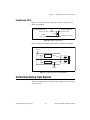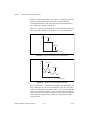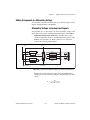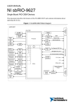
1
DAQ SCB-68 User Manual for Advanced Functions 68-Pin Shielded Desktop Connector Block SCB-68 User Manual for Advanced Functions March 2009 372551A-01 Support Worldwide Technical Support and Product Information ni.com National Instruments Corporate Headquarters 11500 North Mopac Expressway Austin, Texas 78759-3504 USA Tel: 512 683 0100 Worldwide Offices Australia 1800 300 800, Austria 43 662 457990-0, Belgium 32 (0) 2 757 0020, Brazil 55 11 3262 3599, Canada 800 433 3488, China 86 21 5050 9800, Czech Republic 420 224 235 774, Denmark 45 45 76 26 00, Finland 358 (0) 9 725 72511, France 01 57 66 24 24, Germany 49 89 7413130, India 91 80 41190000, Israel 972 3 6393737, Italy 39 02 41309277, Japan 0120-527196, Korea 82 02 3451 3400, Lebanon 961 (0) 1 33 28 28, Malaysia 1800 887710, Mexico 01 800 010 0793, Netherlands 31 (0) 348 433 466, New Zealand 0800 553 322, Norway 47 (0) 66 90 76 60, Poland 48 22 328 90 10, Portugal 351 210 311 210, Russia 7 495 783 6851, Singapore 1800 226 5886, Slovenia 386 3 425 42 00, South Africa 27 0 11 805 8197, Spain 34 91 640 0085, Sweden 46 (0) 8 587 895 00, Switzerland 41 56 2005151, Taiwan 886 02 2377 2222, Thailand 662 278 6777, Turkey 90 212 279 3031, United Kingdom 44 (0) 1635 523545 For further support information, refer to the Technical Support and Professional Services appendix. To comment on National Instruments documentation, refer to the National Instruments Web site at ni.com/info and enter the info code feedback. © 2009 National Instruments Corporation. All rights reserved. Important Information Warranty The SCB-68 is warranted against defects in materials and workmanship for a period of one year from the date of shipment, as evidenced by receipts or other documentation. National Instruments will, at its option, repair or replace equipment that proves to be defective during the warranty period. This warranty includes parts and labor. The media on which you receive National Instruments software are warranted not to fail to execute programming instructions, due to defects in materials and workmanship, for a period of 90 days from date of shipment, as evidenced by receipts or other documentation. National Instruments will, at its option, repair or replace software media that do not execute programming instructions if National Instruments receives notice of such defects during the warranty period. National Instruments does not warrant that the operation of the software shall be uninterrupted or error free. A Return Material Authorization (RMA) number must be obtained from the factory and clearly marked on the outside of the package before any equipment will be accepted for warranty work. National Instruments will pay the shipping costs of returning to the owner parts which are covered by warranty. National Instruments believes that the information in this document is accurate. The document has been carefully reviewed for technical accuracy. In the event that technical or typographical errors exist, National Instruments reserves the right to make changes to subsequent editions of this document without prior notice to holders of this edition. The reader should consult National Instruments if errors are suspected. In no event shall National Instruments be liable for any damages arising out of or related to this document or the information contained in it. EXCEPT AS SPECIFIED HEREIN, NATIONAL INSTRUMENTS MAKES NO WARRANTIES, EXPRESS OR IMPLIED, AND SPECIFICALLY DISCLAIMS ANY WARRANTY OF MERCHANTABILITY OR FITNESS FOR A PARTICULAR PURPOSE. CUSTOMER’S RIGHT TO RECOVER DAMAGES CAUSED BY FAULT OR NEGLIGENCE ON THE PART OF NATIONAL INSTRUMENTS SHALL BE LIMITED TO THE AMOUNT THERETOFORE PAID BY THE CUSTOMER. NATIONAL INSTRUMENTS WILL NOT BE LIABLE FOR DAMAGES RESULTING FROM LOSS OF DATA, PROFITS, USE OF PRODUCTS, OR INCIDENTAL OR CONSEQUENTIAL DAMAGES, EVEN IF ADVISED OF THE POSSIBILITY THEREOF. This limitation of the liability of National Instruments will apply regardless of the form of action, whether in contract or tort, including negligence. Any action against National Instruments must be brought within one year after the cause of action accrues. National Instruments shall not be liable for any delay in performance due to causes beyond its reasonable control. The warranty provided herein does not cover damages, defects, malfunctions, or service failures caused by owner’s failure to follow the National Instruments installation, operation, or maintenance instructions; owner’s modification of the product; owner’s abuse, misuse, or negligent acts; and power failure or surges, fire, flood, accident, actions of third parties, or other events outside reasonable control. Copyright Under the copyright laws, this publication may not be reproduced or transmitted in any form, electronic or mechanical, including photocopying, recording, storing in an information retrieval system, or translating, in whole or in part, without the prior written consent of National Instruments Corporation. National Instruments respects the intellectual property of others, and we ask our users to do the same. NI software is protected by copyright and other intellectual property laws. Where NI software may be used to reproduce software or other materials belonging to others, you may use NI software only to reproduce materials that you may reproduce in accordance with the terms of any applicable license or other legal restriction. Trademarks National Instruments, NI, ni.com, and LabVIEW are trademarks of National Instruments Corporation. Refer to the Terms of Use section on ni.com/legal for more information about National Instruments trademarks. Members of the National Instruments Alliance Partner Program are business entities independent from National Instruments and have no agency, partnership, or joint-venture relationship with National Instruments. Patents For patents covering National Instruments products/technology, refer to the appropriate location: Help»Patents in your software, the patents.txt file on your media, or the National Instruments Patent Notice at ni.com/patents. WARNING REGARDING USE OF NATIONAL INSTRUMENTS PRODUCTS (1) NATIONAL INSTRUMENTS PRODUCTS ARE NOT DESIGNED WITH COMPONENTS AND TESTING FOR A LEVEL OF RELIABILITY SUITABLE FOR USE IN OR IN CONNECTION WITH SURGICAL IMPLANTS OR AS CRITICAL COMPONENTS IN ANY LIFE SUPPORT SYSTEMS WHOSE FAILURE TO PERFORM CAN REASONABLY BE EXPECTED TO CAUSE SIGNIFICANT INJURY TO A HUMAN. (2) IN ANY APPLICATION, INCLUDING THE ABOVE, RELIABILITY OF OPERATION OF THE SOFTWARE PRODUCTS CAN BE IMPAIRED BY ADVERSE FACTORS, INCLUDING BUT NOT LIMITED TO FLUCTUATIONS IN ELECTRICAL POWER SUPPLY, COMPUTER HARDWARE MALFUNCTIONS, COMPUTER OPERATING SYSTEM SOFTWARE FITNESS, FITNESS OF COMPILERS AND DEVELOPMENT SOFTWARE USED TO DEVELOP AN APPLICATION, INSTALLATION ERRORS, SOFTWARE AND HARDWARE COMPATIBILITY PROBLEMS, MALFUNCTIONS OR FAILURES OF ELECTRONIC MONITORING OR CONTROL DEVICES, TRANSIENT FAILURES OF ELECTRONIC SYSTEMS (HARDWARE AND/OR SOFTWARE), UNANTICIPATED USES OR MISUSES, OR ERRORS ON THE PART OF THE USER OR APPLICATIONS DESIGNER (ADVERSE FACTORS SUCH AS THESE ARE HEREAFTER COLLECTIVELY TERMED “SYSTEM FAILURES”). ANY APPLICATION WHERE A SYSTEM FAILURE WOULD CREATE A RISK OF HARM TO PROPERTY OR PERSONS (INCLUDING THE RISK OF BODILY INJURY AND DEATH) SHOULD NOT BE RELIANT SOLELY UPON ONE FORM OF ELECTRONIC SYSTEM DUE TO THE RISK OF SYSTEM FAILURE. TO AVOID DAMAGE, INJURY, OR DEATH, THE USER OR APPLICATION DESIGNER MUST TAKE REASONABLY PRUDENT STEPS TO PROTECT AGAINST SYSTEM FAILURES, INCLUDING BUT NOT LIMITED TO BACK-UP OR SHUT DOWN MECHANISMS. BECAUSE EACH END-USER SYSTEM IS CUSTOMIZED AND DIFFERS FROM NATIONAL INSTRUMENTS' TESTING PLATFORMS AND BECAUSE A USER OR APPLICATION DESIGNER MAY USE NATIONAL INSTRUMENTS PRODUCTS IN COMBINATION WITH OTHER PRODUCTS IN A MANNER NOT EVALUATED OR CONTEMPLATED BY NATIONAL INSTRUMENTS, THE USER OR APPLICATION DESIGNER IS ULTIMATELY RESPONSIBLE FOR VERIFYING AND VALIDATING THE SUITABILITY OF NATIONAL INSTRUMENTS PRODUCTS WHENEVER NATIONAL INSTRUMENTS PRODUCTS ARE INCORPORATED IN A SYSTEM OR APPLICATION, INCLUDING, WITHOUT LIMITATION, THE APPROPRIATE DESIGN, PROCESS AND SAFETY LEVEL OF SUCH SYSTEM OR APPLICATION. Conventions The following conventions are used in this manual: <> Angle brackets that contain numbers separated by an ellipsis represent a range of values associated with a bit or signal name—for example, AO <3..0>. » The » symbol leads you through nested menu items and dialog box options to a final action. The sequence File»Page Setup»Options directs you to pull down the File menu, select the Page Setup item, and select Options from the last dialog box. This icon denotes a note, which alerts you to important information. This icon denotes a caution, which advises you of precautions to take to avoid injury, data loss, or a system crash. bold Bold text denotes items that you must select or click in the software, such as menu items and dialog box options. Bold text also denotes parameter names. italic Italic text denotes variables, emphasis, a cross-reference, or an introduction to a key concept. Italic text also denotes text that is a placeholder for a word or value that you must supply. monospace Text in this font denotes text or characters that you should enter from the keyboard, sections of code, programming examples, and syntax examples. This font is also used for the proper names of disk drives, paths, directories, programs, subprograms, subroutines, device names, functions, operations, variables, filenames, and extensions. Platform Text in this font denotes a specific platform and indicates that the text following it applies only to that platform. Contents Chapter 1 Introduction Related Documentation..................................................................................................1-2 Chapter 2 Temperature Sensor and Thermocouple Using the Temperature Sensor.......................................................................................2-1 Taking Thermocouple Measurements ...........................................................................2-1 Temperature Sensor Output and Accuracy ....................................................................2-2 Thermocouple Sources of Error.....................................................................................2-3 Open Thermocouple Detection ......................................................................................2-4 Thermocouple Input Filtering ........................................................................................2-5 Chapter 3 Soldering and Desoldering Components on the SCB-68 Soldering Equipment .....................................................................................................3-1 Removing the SCB-68 Board from the Base.................................................................3-1 Soldering and Desoldering Guidelines ..........................................................................3-2 Chapter 4 Adding Components for Special Functions Channel Pad Configurations ..........................................................................................4-1 Conditioning Analog Input Channels..............................................................4-2 Conditioning Analog Output Channels ...........................................................4-4 Conditioning PFI 0 ..........................................................................................4-5 Connecting Analog Input Signals ..................................................................................4-5 Connecting Floating Signal Sources ...............................................................4-7 What Are Floating Signal Sources? ..................................................4-7 When to Use Differential Connections with Floating Signal Sources................................................................................4-7 When to Use Non-Referenced Single-Ended (NRSE) Connections with Floating Signal Sources ....................................4-7 When to Use Referenced Single-Ended (RSE) Connections with Floating Signal Sources ....................................4-8 Using Differential Connections for Floating Signal Sources............4-9 Installing Bias Resistors.................................................................................................4-12 © National Instruments Corporation v SCB-68 User Manual for Advanced Functions Contents Filtering ......................................................................................................................... 4-13 Lowpass Filtering............................................................................................ 4-13 One-Pole Lowpass RC Filter ............................................................ 4-16 Selecting Components for Lowpass Filtering .................................. 4-17 Adding Components for Lowpass Filtering ..................................... 4-17 Lowpass Filtering Applications........................................................ 4-20 Highpass Filtering ........................................................................................... 4-23 One-Pole Highpass RC Filter ........................................................... 4-24 Selecting Components for Highpass Filtering.................................. 4-25 Adding Components for Highpass Filtering..................................... 4-25 Highpass Filtering Applications ....................................................... 4-27 Current Input Measurement........................................................................................... 4-28 Selecting a Resistor for Current Input Measurement...................................... 4-29 Adding Components for Current Input Measurement .................................... 4-29 Attenuating Voltage....................................................................................................... 4-31 Selecting Components for Attenuating Voltage ............................................. 4-32 Accuracy Considerations for Attenuating Voltage........................... 4-32 Adding Components for Attenuating Voltage ................................................ 4-33 Attenuating Voltage on Analog Input Signals.................................. 4-33 Attenuating Voltage on Analog Output Signals ............................... 4-35 Attenuating Voltage on Digital Inputs.............................................. 4-35 Voltage Dividers ............................................................................................. 4-36 Voltage Dividers for Analog Input ................................................... 4-36 Voltage Dividers for Analog Output ................................................ 4-37 Voltage Dividers for Digital Inputs .................................................. 4-37 Adding Power Filters..................................................................................................... 4-38 Appendix A Specifications Appendix B Technical Support and Professional Services Index SCB-68 User Manual for Advanced Functions vi ni.com 1 Introduction The SCB-68 is a shielded I/O connector block with 68 screw terminals for easy signal connection to a National Instruments 68-pin or 100-pin DAQ device. The SCB-68 features a general breadboard area for custom circuitry and sockets for interchanging electrical components. These sockets or component pads allow filtering, 4 to 20 mA current input measurement, open thermocouple detection, and voltage attenuation. The open component pads allow you to easily add signal conditioning to the analog input (AI), analog output (AO), and PFI 0 signals of a 68-pin or 100-pin DAQ device. 1 2 5 3 10 8 4 5 6 9 1 2 3 4 Quick Reference Label Top Cover 68-Pin Connector Screws Lock Washers 8 7 5 6 7 Shielding Screws 68-Pin I/O Connector Base 8 Strain-Relief Screws 9 Strain-Relief Hardware 10 SCB-68 Board Assembly Figure 1-1. SCB-68 Parts Locator Diagram © National Instruments Corporation 1-1 SCB-68 User Manual for Advanced Functions Chapter 1 Introduction This document contains information about advanced functions of the SCB-68. Refer to the following chapters for detailed information: • Chapter 2, Temperature Sensor and Thermocouple, features information about using the temperature sensor, taking thermocouple measurements, open thermocouple detection, and thermocouple input filtering. • Chapter 3, Soldering and Desoldering Components on the SCB-68 • Chapter 4, Adding Components for Special Functions, features information about installing bias resistors, filtering, current input measurement, attenuating voltage, and adding power filters. • Appendix A, Specifications Related Documentation For more information about using the SCB-68 with your DAQ device, refer to the following resources: • Documentation for your DAQ device at ni.com/manuals • Measurement & Automation Explorer Help • DAQ Getting Started Guide • NI KnowledgeBase at ni.com/kb • NI Developer Zone at ni.com/zone • SCB-68 User Guide, included in your SCB-68 kit and also available at ni.com/manuals, provides information about SCB-68 installation, the temperature sensor and signal conditioning switch configuration, analog input measurement connection, and accessory fuse and power. SCB-68 User Manual for Advanced Functions 1-2 ni.com 2 Temperature Sensor and Thermocouple This chapter covers the following temperature sensor and thermocouple-related topics: • Using the Temperature Sensor • Taking Thermocouple Measurements • Temperature Sensor Output and Accuracy • Thermocouple Sources of Error • Open Thermocouple Detection • Thermocouple Input Filtering Using the Temperature Sensor To accommodate thermocouples with DAQ devices, the SCB-68 has a temperature sensor for cold-junction compensation (CJC), shown in Figure 3-1, SCB-68 Printed Circuit Board Diagram. To power the temperature sensor, set switches S1, S2, and S3 for single-ended or differential mode as described in the Using the SCB-68 with MIO DAQ Devices section of the SCB-68 User Guide. This configuration also powers the signal conditioning area and circuitry. Refer to Figure 4-1, Analog Input and Cold-Junction Compensation Circuitry, for a diagram of the CJC circuitry on the SCB-68. Taking Thermocouple Measurements You can measure thermocouples in differential or single-ended configuration: • © National Instruments Corporation Differential configuration has better noise immunity. Use bias resistors when the DAQ device is in differential input mode, as described in the Installing Bias Resistors section of Chapter 4, Adding Components for Special Functions. 2-1 SCB-68 User Manual for Advanced Functions Chapter 2 Temperature Sensor and Thermocouple • Single-ended configuration has twice as many inputs. For single-ended configuration, set your DAQ device for referenced single-ended (RSE) input mode. The maximum voltage level thermocouples generate is typically only a few millivolts. You should use a DAQ device with high gain for best resolution. For more information about thermocouple measurements, refer to the NI Developer Zone tutorial, Taking Thermocouple Temperature Measurements. To access this document, go to ni.com/info and enter the info code rdtttm. The DAQ device must have a ground reference because thermocouples are floating signal sources. For more information about floating signal sources, refer to the Connecting Analog Input Signals section of Chapter 4, Adding Components for Special Functions. For more information about field wiring, refer to the NI Developer Zone document, Field Wiring and Noise Considerations for Analog Signals. To access this document, go to ni.com/info and enter the info code rdfwn3. CJC with the SCB-68 is accurate only if the temperature sensor reading is close to the actual temperature of the screw terminals. Therefore, when reading thermocouples, keep the SCB-68 away from drafts or other temperature gradients, such as those caused by heaters, radiators, fans, and warm equipment. Temperature Sensor Output and Accuracy The SCB-68 temperature sensor outputs 10 mV/°C and has an accuracy of ±1 °C. You also can determine the temperature using the following formulas: TC = 100 × Vt TK = TC + 273.15 9 T F = --- × T C + 32 5 where Vt is the temperature sensor output voltage; and TC, TK, and TF are the temperature readings in degrees Celsius, Kelvin, and Fahrenheit, respectively. SCB-68 User Manual for Advanced Functions 2-2 ni.com Chapter 2 Temperature Sensor and Thermocouple Thermocouple Sources of Error When taking thermocouple measurements with the SCB-68, the possible sources of error are as follows: • Compensation error—Can arise from two sources—inaccuracy of the temperature sensor and temperature differences between the temperature sensor and the screw terminals. The temperature sensor on the SCB-68 is specified to be accurate to ±1 °C. You can minimize temperature differences between the temperature sensor and the screw terminals by keeping the SCB-68 away from drafts, heaters, and warm equipment. • Linearization error—A consequence of the polynomials being approximations of the true thermocouple output. The linearization error depends upon the degree of polynomial used. • Measurement error—The result of inaccuracies in the DAQ device. These inaccuracies include gain, offset, and noise. Accuracy can be calculated from the DAQ device specifications. For best results, you must use a well-calibrated DAQ device. NI recommends that you run self-calibration on your DAQ device frequently to reduce error. • Thermocouple wire error—The result of inconsistencies in the thermocouple manufacturing process. These inconsistencies, or nonhomogeneities, are the result of defects or impurities in the thermocouple wire. The errors vary depending on the thermocouple type and the gauge of wire used, but an error of ±2 °C is typical. For more information about thermocouple wire errors and more specific data, consult the thermocouple manufacturer. • Noise error—Error due to inherent system noise. Use the average of a large number of samples to obtain the most accurate reading. Noisy environments require averaging more samples for greater accuracy. white noise ------------------------------------------------- = resulting noise number of samples For best results, use the average of at least 100 readings to reduce the effects of noise; typical absolute accuracies should then be about ±2 °C. © National Instruments Corporation 2-3 SCB-68 User Manual for Advanced Functions Chapter 2 Temperature Sensor and Thermocouple Open Thermocouple Detection You can build open thermocouple detection circuitry by connecting a high-value resistor between the positive input and +5 V. A resistor of a few MΩ or more is sufficient, but a high-value resistor allows you to detect an open or defective thermocouple. Refer to Chapter 3, Soldering and Desoldering Components on the SCB-68, for more information about adding components and for soldering and desoldering instructions. Note • Differential analog input open thermocouple detection—Use position A to connect a high-value resistor between the positive input and +5 V. Leave the 0 Ω resistors at positions F and G in place for each channel used. Refer to Table 4-1, Analog Input Channels Component Locations, for component positions for all analog input channels. +5 V AI <i> (A) (F) (B) (E) (G) (C) (D) AI GND AI <i+8> Figure 2-1. Differential Analog Input Open Thermocouple Detection • Single-ended analog input open thermocouple detection—Use position A for one channel and C for the next channel when you connect a high-value resistor between the positive input and +5 V. Leave the 0 Ω resistors at positions F and G in place for each channel used. Refer to Table 4-1, Analog Input Channels Component Locations, for component positions for all analog input channels. SCB-68 User Manual for Advanced Functions 2-4 ni.com Chapter 2 +5 V Temperature Sensor and Thermocouple AI <i> (A) (F) (B) (E) (G) (C) (D) AI GND AI <i+8> Figure 2-2. Single-Ended Analog Input Open Thermocouple Detection on AI <i> If the thermocouple opens, the voltage measured across the input terminals rises to +5 V, a value much larger than any legitimate thermocouple voltage. You can create a bias current return path by using a 100 kΩ resistor between the negative input and AI GND. Thermocouple Input Filtering To reduce noise, you can connect a simple one-pole RC lowpass filter to the analog inputs of the SCB-68. Refer to the Lowpass Filtering section of Chapter 4, Adding Components for Special Functions, for more information. © National Instruments Corporation 2-5 SCB-68 User Manual for Advanced Functions Soldering and Desoldering Components on the SCB-68 3 Some applications require you to make modifications to the SCB-68, usually in the form of adding components to the printed circuit device. Note Some versions of the SCB-68 have 0 Ω resistors hardwired in the factory-default positions. In such cases, to move these resistors to and from the factory-default positions, you must solder and desolder on the SCB-68 circuit card assembly. Soldering Equipment To solder components on the SCB-68, you need the following: ❑ Phillips #1 and #2 screwdrivers ❑ 0.125 in. flathead screwdriver ❑ Soldering iron and solder ❑ Long nose pliers ❑ Components specific to your application Removing the SCB-68 Board from the Base Refer to Figure 1-1, SCB-68 Parts Locator Diagram, while completing the following steps to remove the SCB-68 from the base. 1. Disconnect the 68-pin cable from the SCB-68, if connected. 2. Remove the shielding screws on either side of the top cover with a Phillips #1 screwdriver, then open the box. 3. Loosen the strain-relief screws with a Phillips #2 screwdriver. 4. Remove the signal wires from screw terminals with a flathead screwdriver. 5. Remove the device-mount screws with a Phillips #1 screwdriver. © National Instruments Corporation 3-1 SCB-68 User Manual for Advanced Functions Chapter 3 Soldering and Desoldering Components on the SCB-68 6. Remove the 68-pin connector screws with a flathead screwdriver. 7. Tilt the SCB-68 up and pull it out. To reinstall the SCB-68, reverse the order of the steps. Soldering and Desoldering Guidelines As you solder and desolder components on the SCB-68, refer to Figure 3-1. 1 2 RC16(B) R27(C) R8(F) RC6(E) R9(G) RC17(D) R28(A) RC18(B) R29(C) R38 R30(A) RC20(B) R31(C) R12(F) RC8(E) R13(G) RC21(D) R32(A) RC22(B) R11(G) C3 11 RC7(E) C5 RC19(D) R10(F) R14(F) RC9(E) R33(C) 10 R15(G) RC23(D) R34(A) RC10(E) R35(C) R17(G) RC25(D) R36(A) RC26(B) R18(F) RC11(E) R37(C) RC27(D) R19(G) RC2 R2 RC3 R10 RC1 RC24(B) R16(F) R3 © 1 2 3 4 +5 V Power Pads R20 and R21 Switches S3, S4, and S5 68-Pin I/O Connector Breadboard Area 5 6 7 8 1 35 2 36 3 37 4 38 5 39 6 40 7 41 8 42 9 43 10 44 11 45 7 S/N SCB-68 COPYRIGHT 1993 7 6 S2 ASSY182470-01 REV.B R7(G) RC15(D) R26(A) 12 46 13 47 14 48 15 49 16 50 17 51 18 52 19 53 20 54 21 55 22 56 C1 R6(F) RC5(E) C2 R5(G) 1 3 RC14(B) R25(C) 5 S1 68 34 67 33 66 32 65 31 64 30 63 29 62 28 61 27 60 26 59 25 58 24 57 23 RC4(E) RC13(D) R24(A) J1 33 34 S5 S4 S3 R4(F) R22(A) 4 XF1 C6 R20 R21 C4 RC12(B) R23(C) 10 3 4 7 Fuse Switches S1 and S2 Screw Terminals PFI 0 Pads 9 8 9 Analog Output Pads 10 Analog Input Pads 11 Temperature Sensor Figure 3-1. SCB-68 Printed Circuit Board Diagram SCB-68 User Manual for Advanced Functions 3-2 ni.com Chapter 3 Note Soldering and Desoldering Components on the SCB-68 If the kit is missing any of the components in Figure 3-1, contact NI. The SCB-68 ships with 0 Ω resistors in the F and G positions. You must remove the resistors to use the positions. Use a low-wattage soldering iron (20 to 30 W) when soldering to the SCB-68. To desolder on the SCB-68, vacuum-type tools work best. Be careful to avoid damaging the component pads when desoldering. Use only rosin-core electronic-grade solder because acid-core solder damages the printed-circuit device and components. © National Instruments Corporation 3-3 SCB-68 User Manual for Advanced Functions Adding Components for Special Functions 4 This chapter describes how to condition signals by adding components to the open component locations of the SCB-68. This chapter describes the following signal conditioning applications: • Installing Bias Resistors (analog input) • Filtering (analog input, analog output, and digital input) • Current Input Measurement (analog input) • Attenuating Voltage (analog input, analog output, and digital input) • Adding Power Filters Caution Add components at your own risk. NI is not liable for any damage resulting from improperly added components. In addition to the applications described in this chapter, you can build many other types of signal conditioning using the component pads and the general-purpose breadboard area of the SCB-68. Refer to Chapter 3, Soldering and Desoldering Components on the SCB-68, for more information about adding components and for soldering and desoldering instructions. After building one of the applications described in this chapter or your custom circuitry, refer to the Getting Started with the SCB-68 section of the SCB-68 User Guide for instructions about how to configure the SCB-68 in Measurement & Automation Explorer (MAX). You can create virtual channels in MAX to create a custom scale or map your voltage ranges to the type of transducer that you use. Channel Pad Configurations When you use the SCB-68 with a 68-pin or 100-pin MIO DAQ device, you can use the component pads on the SCB-68 to condition 16 AI channels, two AO channels, and PFI 0. © National Instruments Corporation 4-1 SCB-68 User Manual for Advanced Functions Chapter 4 Adding Components for Special Functions Conditioning Analog Input Channels Figure 4-1 shows the analog input and CJC circuitry on the SCB-68. +5 V R22 AI 0 Screw Terminal (I/O Pin 56) R4 CJC Not Used RC12 + AI GND User-Configurable +5 V AI 0 (I/O Pin 68) S5 CJC Used C3 (0.1 μF) Q1 R38 AI C5 (1 μF) +5 V AI R23 R5 AI 8 (I/O Pin 34) RSE CJC or Non-MIO S4 DIFF CJC + RC13 AI AI 8 Screw Terminal (I/O Pin 56) AI GND User-Configurable Figure 4-1. Analog Input and Cold-Junction Compensation Circuitry Figure 4-2 illustrates the AI channel configuration. You can use AI <i> and AI <i+8> as either a differential channel pair or as two single-ended channels. To use the SCB-68 with ground-referenced single-ended inputs, do not use the open positions that connect the input to AI GND, positions B and D, for grounded sources as shown in Figure 4-2. Build any signal conditioning circuitry requiring a ground reference in the custom breadboard area using AI SENSE as the ground reference instead of building the circuitry in the open component positions. SCB-68 User Manual for Advanced Functions 4-2 ni.com Chapter 4 Adding Components for Special Functions Note Some versions of the SCB-68 have 0 Ω resistors hardwired in the factory-default positions. In such cases, to move these resistors to and from the factory-default positions, you must solder and desolder on the SCB-68 circuit card assembly. When soldering, refer to Chapter 3, Soldering and Desoldering Components on the SCB-68. +5 V AI <i> (A) (F) (B) (E) (G) (C) (D) AI GND AI <i+8> Figure 4-2. Analog Input Channel Pad Configuration for AI <i> and AI <i+8> Table 4-1 correlates the component labels of the SCB-68 to component locations A through G for differential channels 0 through 7. Table 4-1. Analog Input Channels Component Locations Channel Single-Ended Differential A B C D E F G AI 0, AI 8 AI 0 R22 RC12 R23 RC13 RC4 R4 R5 AI 1, AI 9 AI 1 R24 RC14 R25 RC15 RC5 R6 R7 AI 2, AI 10 AI 2 R26 RC16 R27 RC17 RC6 R8 R9 AI 3, AI 11 AI 3 R28 RC18 R29 RC19 RC7 R10 R11 AI 4, AI 12 AI 4 R30 RC20 R31 RC21 RC8 R12 R13 AI 5, AI 13 AI 5 R32 RC22 R33 RC23 RC9 R14 R15 AI 6, AI 14 AI 6 R34 RC24 R35 RC25 RC10 R16 R17 AI 7, AI 15 AI 7 R36 RC26 R37 RC27 RC11 R18 R19 R denotes a socket for one component. RC denotes sockets for two components to be connected in parallel. © National Instruments Corporation 4-3 SCB-68 User Manual for Advanced Functions Chapter 4 Adding Components for Special Functions Conditioning Analog Output Channels Figure 4-3 shows the circuitry for both analog output channels on the SCB-68. R3 AO 0 (I/O Pin 22) AO 0 Screw Terminal RC3 AO GND (I/O Pin 55) AO GND Screw Terminal R2 AO 1 (I/O Pin 21) AO 1 Screw Terminal RC2 AO GND (I/O Pin 54) AO GND Screw Terminal Figure 4-3. Analog Output Circuitry Figure 4-4 illustrates the generic AO channel pad configuration. (B) AO GND (A) AO Figure 4-4. Analog Output Channel Pad Configuration Table 4-2 correlates the component labels of the SCB-68 to component locations A and B for analog output channels 0 and 1. Table 4-2. Analog Output Channels Component Locations Channel A B AO 0 R3 RC3 AO 1 R2 RC2 R denotes a socket for one component. RC denotes sockets for two components to be connected in parallel. SCB-68 User Manual for Advanced Functions 4-4 ni.com Chapter 4 Adding Components for Special Functions Conditioning PFI 0 Figure 4-5 shows the shows the digital input channel configuration for PFI 0 on the SCB-68. R1 PFI 0/AI START TRIG (I/O Pin 11) PFI 0/AI START TRIG Screw Terminal RC1 D GND (I/O Pin 44) D GND Screw Terminal Figure 4-5. Digital Trigger Circuitry Figure 4-6 illustrates the digital input channel configuration for PFI 0. PFI 0 (R1) 11 44 (RC1) D GND Figure 4-6. Digital Input Channel Pad Configuration Connecting Analog Input Signals Table 4-3 summarizes the recommended input configuration for both types of signal sources. © National Instruments Corporation 4-5 SCB-68 User Manual for Advanced Functions Chapter 4 Adding Components for Special Functions Table 4-3. Analog Input Configuration Floating Signal Sources (Not Connected to Building Ground) AI Ground-Reference Setting* Differential (DIFF) Ground-Referenced Signal Sources* Examples: Example: • Ungrounded thermocouples • Plug-in instruments with non-isolated outputs • Signal conditioning with isolated outputs • Battery devices Signal Source DAQ Device AI+ + – AI– Signal Source DAQ Device AI+ + + – – AI– AI GND Non-Referenced Single-Ended (NRSE) Signal Source DAQ Device AI + – Signal Source DAQ Device AI + + – – – AI GND NOT RECOMMENDED DAQ Device AI + – Signal Source DAQ Device + AI + – – AI GND + AI SENSE AI GND Signal Source – AI GND AI SENSE Referenced Single-Ended (RSE) + VA + – VB AI GND Ground-loop potential (VA – VB) are added to measured signal. * Refer to the documentation for your DAQ device for descriptions of the RSE, NRSE, and DIFF modes, analog input signal sources, and software considerations. SCB-68 User Manual for Advanced Functions 4-6 ni.com Chapter 4 Adding Components for Special Functions Connecting Floating Signal Sources What Are Floating Signal Sources? A floating signal source is not connected to the building ground system, but has an isolated ground-reference point. Some examples of floating signal sources are outputs of transformers, thermocouples, battery-powered devices, optical isolators, and isolation amplifiers. An instrument or device that has an isolated output is a floating signal source. When to Use Differential Connections with Floating Signal Sources Use differential input connections for any channel that meets any of the following conditions: • The input signal is low-level (less than 1 V). • The leads connecting the signal to the device are greater than 3 m (10 ft). • The input signal requires a separate ground-reference point or return signal. • The signal leads travel through noisy environments. • Two analog input channels, AI+ and AI–, are available for the signal. Differential signal connections reduce noise pickup and increase common-mode noise rejection. Differential signal connections also allow input signals to float within the common-mode limits of the NI-PGIA. Refer to the Using Differential Connections for Floating Signal Sources section for more information about differential connections. When to Use Non-Referenced Single-Ended (NRSE) Connections with Floating Signal Sources Only use NRSE input connections if the input signal meets the following conditions: • The input signal is high-level (greater than 1 V). • The leads connecting the signal to the device are less than 3 m (10 ft). Differential input connections are recommended for greater signal integrity for any input signal that does not meet the preceding conditions. © National Instruments Corporation 4-7 SCB-68 User Manual for Advanced Functions Chapter 4 Adding Components for Special Functions In the single-ended modes, more electrostatic and magnetic noise couples into the signal connections than in differential configurations. The coupling is the result of differences in the signal path. Magnetic coupling is proportional to the area between the two signal conductors. Electrical coupling is a function of how much the electric field differs between the two conductors. With this type of connection, the NI-PGIA rejects both the common-mode noise in the signal and the ground potential difference between the signal source and the device ground. Refer to the documentation for your DAQ device for more information about NRSE connections. When to Use Referenced Single-Ended (RSE) Connections with Floating Signal Sources Only use RSE input connections if the input signal meets the following conditions: • The input signal can share a common reference point, AI GND, with other signals that use RSE. • The input signal is high-level (greater than 1 V). • The leads connecting the signal to the device are less than 3 m (10 ft). Differential input connections are recommended for greater signal integrity for any input signal that does not meet the preceding conditions. In the single-ended modes, more electrostatic and magnetic noise couples into the signal connections than in differential configurations. The coupling is the result of differences in the signal path. Magnetic coupling is proportional to the area between the two signal conductors. Electrical coupling is a function of how much the electric field differs between the two conductors. With this type of connection, the NI-PGIA rejects both the common-mode noise in the signal and the ground potential difference between the signal source and the device ground. Refer to the documentation for your DAQ device for more information about RSE connections. SCB-68 User Manual for Advanced Functions 4-8 ni.com Chapter 4 Adding Components for Special Functions Using Differential Connections for Floating Signal Sources It is important to connect the negative lead of a floating source to AI GND (either directly or through a bias resistor). Otherwise, the source can float out of the maximum working voltage range of the NI-PGIA and the DAQ device returns erroneous data. The easiest way to reference the source to AI GND is to connect the positive side of the signal to AI+ and connect the negative side of the signal to AI GND as well as to AI– without using resistors. This connection works well for DC-coupled sources with low source impedance (<100 Ω). DAQ Device AI+ Floating Signal Source + Vs – AI– Inpedance <100 Ω AI SENSE AI GND Figure 4-7. Differential Connections for Floating Signal Sources without Bias Resistors However, for larger source impedances, this connection leaves the differential signal path significantly off balance. Noise that couples electrostatically onto the positive line does not couple onto the negative line because it is connected to ground. This noise appears as a differential mode signal instead of a common-mode signal, and thus appears in your data. In this case, instead of directly connecting the negative line to AI GND, connect the negative line to AI GND through a resistor that is about 100 times the equivalent source impedance. The resistor puts the signal path nearly in balance, so that about the same amount of noise couples onto both connections, yielding better rejection of electrostatically coupled noise. This configuration does not load down the source (other than the very high input impedance of the NI-PGIA). © National Instruments Corporation 4-9 SCB-68 User Manual for Advanced Functions Chapter 4 Adding Components for Special Functions DAQ Device AI+ Floating Signal Source + Vs – AI– R is about 100 times source impedance of sensor R AI SENSE AI GND Figure 4-8. Differential Connections for Floating Signal Sources with Single Bias Resistor You can fully balance the signal path by connecting another resistor of the same value between the positive input and AI GND, as shown in Figure 4-9. This fully balanced configuration offers slightly better noise rejection, but has the disadvantage of loading the source down with the series combination (sum) of the two resistors. If, for example, the source impedance is 2 kΩ and each of the two resistors is 100 kΩ, the resistors load down the source with 200 kΩ and produce a –1% gain error. SCB-68 User Manual for Advanced Functions 4-10 ni.com Chapter 4 Adding Components for Special Functions AI+ Floating Signal Source + Bias Resistors (see text) Instrumentation Amplifier + Vs – PGIA + AI– – Vm Measured Voltage – Bias Current Return Paths Input Multiplexers AI SENSE AI GND I/O Connector DAQ Device Configured in Differential Mode Figure 4-9. Differential Connections for Floating Signal Sources with Balanced Bias Resistors Both inputs of the NI-PGIA require a DC path to ground in order for the NI-PGIA to work. If the source is AC coupled (capacitively coupled), the NI-PGIA needs a resistor between the positive input and AI GND. If the source has low-impedance, choose a resistor that is large enough not to significantly load the source, but small enough not to produce significant input offset voltage as a result of input bias current (typically 100 kΩ to 1 MΩ). In this case, connect the negative input directly to AI GND. If the source has high output impedance, balance the signal path as previously described using the same value resistor on both the positive and negative inputs; be aware that there is some gain error from loading down the source, as shown in Figure 4-10. © National Instruments Corporation 4-11 SCB-68 User Manual for Advanced Functions Chapter 4 Adding Components for Special Functions AC Coupling AC Coupled Floating Signal Source DAQ Device AI+ + Vs – AI– AI SENSE AI GND Figure 4-10. Differential Connections for AC Coupled Floating Sources with Balanced Bias Resistors Refer to the Installing Bias Resistors section for information about installing bias resistors on the SCB-68. Installing Bias Resistors To install a single bias resistor on the negative line (AI–) of a differential pair, put the resistor in position D on the SCB-68, as shown in Figure 4-11. +5 V AI <i> (A) (B) (F) (E) (C) (G) (D) AI GND AI <i+8> Figure 4-11. AI Differential Configuration with Single Bias Resistor SCB-68 User Manual for Advanced Functions 4-12 ni.com Chapter 4 Adding Components for Special Functions To install balanced bias resistors, put resistors in positions B and D on the SCB-68, as shown in Figure 4-12. +5 V AI <i> (A) (B) (F) (E) (G) (C) (D) AI GND AI <i+8> Figure 4-12. AI Differential Configuration with Balanced Bias Resistors Filtering This section discusses lowpass and highpass filtering on the SCB-68. Lowpass Filtering This section discusses the following topics regarding lowpass filtering on the SCB-68: • One-Pole Lowpass RC Filter • Selecting Components for Lowpass Filtering • Adding Components for Lowpass Filtering • Lowpass Filtering Applications Lowpass filters highly or completely attenuate signals with frequencies above the cut-off frequency, or high-frequency stopband signals. Lowpass filters do not attenuate signals with frequencies below the cut-off frequency, or low-frequency passband signals. Ideally, lowpass filters have a phase shift that is linear with respect to frequency. This linear phase shift delays signal components of all frequencies by a constant time, independent of frequency, thereby preserving the overall shape of the signal. © National Instruments Corporation 4-13 SCB-68 User Manual for Advanced Functions Chapter 4 Adding Components for Special Functions In practice, lowpass filters subject input signals to a mathematical transfer function that approximates the characteristics of an ideal filter. By analyzing the Bode Plot, or the plot that represents the transfer function, you can determine the filter characteristics. Gain Figures 4-13 and 4-14 show the Bode Plots for the ideal filter and the real filter, respectively, and indicate the attenuation of each transfer function. Passband Stopband fc Log Frequency Gain Figure 4-13. Transfer Function Attenuation for an Ideal Filter Passband Stopband Transition Region fc Log Frequency Figure 4-14. Transfer Function Attenuation for a Real Filter The cut-off frequency, fc, is defined as the frequency beyond which the gain drops 3 dB. Figure 4-13 shows how an ideal filter causes the gain to drop to zero for all frequencies greater than fc. Thus, fc does not pass through the filter to its output. Instead of having a gain of absolute zero for frequencies greater than fc, the real filter has a transition region between the passband and the stopband, a ripple in the passband, and a stopband with a finite attenuation gain. SCB-68 User Manual for Advanced Functions 4-14 ni.com Chapter 4 Adding Components for Special Functions Volts (V) Real filters have some nonlinearity in their phase response, causing signals at higher frequencies to be delayed longer than signals at lower frequencies and resulting in an overall shape distortion of the signal. For example, when the square wave, shown in Figure 4-15, enters a filter, an ideal filter smooths the edges of the input, whereas a real filter causes some ringing in the signal as the higher frequency components of the signal are delayed. Time (t) Figure 4-15. Square Wave Input Signal Volts (V) Figures 4-16 and 4-17 show the difference in response to a square wave between an ideal and a real filter, respectively. Time (t) Figure 4-16. Response of an Ideal Filter to a Square Wave Input Signal © National Instruments Corporation 4-15 SCB-68 User Manual for Advanced Functions Adding Components for Special Functions Volts (V) Chapter 4 Time (t) Figure 4-17. Response of a Real Filter to a Square Wave Input Signal One-Pole Lowpass RC Filter Figure 4-18 shows the transfer function of a simple series circuit consisting of a resistor (R) and capacitor (C) when the voltage across R is assumed to be the output voltage (Vm). R Vin C Vm Figure 4-18. Simple RC Lowpass Filter The transfer function is a mathematical representation of a one-pole lowpass filter, with a time constant of: 1 -------------2πRC Use Equation 4-1 to design a lowpass filter for a simple resistor and capacitor circuit, where the values of the resistor and capacitor alone determine fc : G T ( s ) = ------------------------------1 + ( 2πRC )s (4-1) where G is the DC gain and s represents the frequency domain. SCB-68 User Manual for Advanced Functions 4-16 ni.com Chapter 4 Adding Components for Special Functions Selecting Components for Lowpass Filtering To determine the value of the components in the circuit, fix R (10 kΩ is reasonable) and isolate C from Equation 4-1 as follows: 1 C = --------------2πRfc (4-2) The cut-off frequency in Equation 4-2 is fc. For best results, choose a resistor that has the following characteristics: • Low wattage of approximately 0.125 W • Precision of at least 5% • Temperature stability • Tolerance of 5% • AXL package (suggested) • Carbon or metal film (suggested) Choose a capacitor that has the following suggested characteristics: • AXL or RDL package • Tolerance of 20% • Maximum voltage of at least 25 V Adding Components for Lowpass Filtering Using the circuit shown in Figure 4-18, you can use a two-component circuit to build a simple RC filter with analog input, analog output, or digital input. Lowpass Filters on Analog Input Signals You can build a lowpass filter for the following analog input modes: • © National Instruments Corporation Differential analog input lowpass filter—To build a differential lowpass filter, refer to Figure 4-19. Add the resistor to position F and the capacitor to position E. Refer to Table 4-1 for component positions for all analog input channels. 4-17 SCB-68 User Manual for Advanced Functions Chapter 4 Adding Components for Special Functions +5 V AI <i> (A) (F) (B) (E) (G) (C) (D) AI GND AI <i+8> Figure 4-19. SCB-68 Circuit Diagram for Differential Analog Input Lowpass Filter • Single-ended analog input lowpass filter—To build a single-ended lowpass filter, refer to Figure 4-20. Add the resistor to position F or G, depending on the AI channel you are using. Add the capacitor to position B or D, depending on the AI channel you are using. Refer to Table 4-1 for component positions for all analog input channels. Filtering increases the settling time of the instrumentation amplifier to the time constant of the filter used. Adding RC filters to scanning channels greatly reduces the practical scanning rate, since the instrumentation amplifier settling time can be increased to 10T or longer, where T = (R)(C). Note +5 V AI <i> (A) (F) (B) (E) (G) (C) (D) AI GND AI <i+8> Figure 4-20. SCB-68 Circuit Diagram for Single-Ended Analog Input Lowpass Filter on AI <i> SCB-68 User Manual for Advanced Functions 4-18 ni.com Chapter 4 Adding Components for Special Functions Lowpass Smoothing Filters on Analog Output Signals To build a lowpass filter for analog output, put a resistor in position A and a capacitor in position B, as shown in Figure 4-21. Refer to Table 4-2 for component positions for both analog output channels. (B) AO GND (A) AO Figure 4-21. SCB-68 Circuit Diagram for Analog Output Lowpass Filter Lowpass Digital Filters on Digital Trigger Input Signals For PFI 0, add the resistor to position R1 and the capacitor to position RC1. Refer to Figure 4-22 for the digital input channel pad configuration. PFI 0 (R1) 11 44 (RC1) D GND Figure 4-22. SCB-68 Circuit Diagram for Digital Trigger Input Lowpass Filter © National Instruments Corporation 4-19 SCB-68 User Manual for Advanced Functions Chapter 4 Adding Components for Special Functions Lowpass Filtering Applications The following sections list applications where lowpass filtering can be useful. Analog Input Lowpass Filtering Applications The following applications benefit from lowpass filtering: • Noise filtering—You can use a lowpass filter to highly attenuate the noise frequency on a measured signal. For example, power lines commonly add a noise frequency of 60 Hz. Adding a filter with fc<60 Hz at the input of the measurement system causes the noise frequency to fall into the stopband. Referring to Equation 4-2, fix the resistor value at 10 kΩ to calculate the capacitor value and choose a commercial capacitor value that satisfies the following relationship: 1 C > ----------------------------------------2π ( 10, 000 ) ( 60 ) • (4-3) Antialiasing filtering—Aliasing causes high-frequency signal components to appear as a low-frequency signal, as Figure 4-23 shows. 1 –1 0 2 4 6 8 10 Input Signal Sampled Points Reconstructed Signal Figure 4-23. Aliasing of a High-Frequency Signal The solid line depicts a high-frequency signal being sampled at the indicated points. When these points are connected to reconstruct the waveform, as shown by the dotted line, the signal appears to have a lower frequency. Any signal with a frequency greater than one-half of its sample rate is aliased and incorrectly analyzed as having a SCB-68 User Manual for Advanced Functions 4-20 ni.com Chapter 4 Adding Components for Special Functions frequency below one-half the sample rate. This limiting frequency of one-half the sample rate is called the Nyquist frequency. To prevent aliasing, remove all signal components with frequencies greater than the Nyquist frequency from input signals before those signals are sampled. Once a data sample is aliased, it is impossible to accurately reconstruct the original signal. To design a lowpass filter that attenuates signal components with a frequency higher than half of the Nyquist frequency, substitute the half Nyquist value for the fc value in Equation 4-3. Note (NI PCI/PXI-6115/6120/6289 Devices Only) NI PCI/PXI-6115/6120 and NI PCI/PXI-6289 devices provide filters and may not need antialiasing filters implemented at the SCB-68 terminal block. Refer to your device documentation for more information. Analog Output Lowpass Filtering Applications The following applications benefit from lowpass filtering: Protection for external circuitry—Lowpass filters can smooth stairstep-like curves on AO signals. If the curves are not smoothed, the AO signals can be a hazard for some external circuitry connected to it. Figure 4-24 shows the output of a lowpass filter when a stairstep-like signal is the input. Volts (V) • Time (t) Figure 4-24. Lowpass Filtering of AO Signals • © National Instruments Corporation Deglitching analog output signals—Lowpass filters can be used to decrease glitches from an analog output signal. When you use a DAC to generate a waveform, you may observe glitches on the output signal. These glitches are normal; when a DAC switches from one voltage to another, it produces glitches due to released charges. The largest 4-21 SCB-68 User Manual for Advanced Functions Chapter 4 Adding Components for Special Functions glitches occur when the most significant bit of the DAC code changes. You can build a lowpass deglitching filter to remove some of these glitches, depending on the frequency and nature of the output signal. To select a cutoff frequency for the deglitching filter, refer to your DAQ device documentation for the maximum glitch duration. PFI 0 Lowpass Filtering Applications Volts (V) Lowpass filters can function as debouncing filters to smooth noise on digital trigger input signals, thus enabling the trigger-detection circuitry of the DAQ device to understand the signal as a valid digital trigger. TTL Logic High TTL Logic Low Time (t) Figure 4-25. Digital Trigger Input Signal with a High-Frequency Component Volts (V) Apply a lowpass filter to the signal to remove the high-frequency component for a cleaner digital signal, as Figure 4-26 shows. Time (t) Figure 4-26. Lowpass Filtering of Digital Trigger Input Signals SCB-68 User Manual for Advanced Functions 4-22 ni.com Chapter 4 Adding Components for Special Functions Due to the filter order, the digital trigger input signal is delayed for a specific amount of time depending on the filter you use before the DAQ device senses the signal at the trigger input. Note Highpass Filtering This section discusses the following topics regarding highpass filtering on the SCB-68: • One-Pole Highpass RC Filter • Selecting Components for Highpass Filtering • Adding Components for Highpass Filtering • Highpass Filtering Applications Highpass filters highly or completely attenuate signals with frequencies below the cut-off frequency, or low-frequency stopband signals. Highpass filters do not attenuate signals with frequencies above the cut-off frequency, or high-frequency passband signals. The cut-off frequency, fc, is defined as the frequency below which the gain drops 3 dB. Figure 4-27 shows how an ideal filter causes the gain to drop to zero for all frequencies less than fc. Thus, fc does not pass through the filter to its output. In practice, highpass filters subject input signals to a mathematical transfer function that approximates the characteristics of an ideal filter. By analyzing the Bode Plot, or the plot that represents the transfer function, you can determine the filter characteristics. Gain Figures 4-27 and 4-28 show the Bode Plots for the ideal filter and the real filter, respectively, and indicate the attenuation of each transfer function. Passband Stopband fc Log Frequency Figure 4-27. Transfer Function Attenuation for an Ideal Filter © National Instruments Corporation 4-23 SCB-68 User Manual for Advanced Functions Adding Components for Special Functions Gain Chapter 4 Passband Stopband Transition Region fc Log Frequency Figure 4-28. Transfer Function Attenuation for a Real Filter Instead of having a gain of absolute zero for frequencies less than fc, the real filter has a transition region between the passband and the stopband, a ripple in the passband, and a stopband with a finite attenuation gain. One-Pole Highpass RC Filter Figure 4-29 shows the transfer function of a simple series circuit consisting of a resistor (R) and capacitor (C) when the voltage across R is assumed to be the output voltage (Vm). C Vin R Vout Figure 4-29. Simple RC Highpass Circuit The transfer function is a mathematical representation of a one-pole highpass filter, with a time constant of: 1 -------------2πRC SCB-68 User Manual for Advanced Functions 4-24 ni.com Chapter 4 Adding Components for Special Functions Use Equation 4-4 to design a lowpass filter for a simple resistor and capacitor circuit, where the values of the resistor and capacitor alone determine fc : G T ( s ) = ------------------------------1 + ( 2πRC )s (4-4) where G is the DC gain and s represents the frequency domain. Selecting Components for Highpass Filtering To determine the value of the components in the circuit, fix R (10 kΩ is reasonable) and isolate C from Equation 4-4 as follows: 1 C = --------------2πRfc (4-5) The cutoff frequency in Equation 4-5 is fc. For best results, choose a resistor that has the following characteristics: • Low wattage of approximately 0.125 W • Precision of at least 5% • Temperature stability • Tolerance of 5% • AXL package (suggested) • Carbon or metal film (suggested) Choose a capacitor that has the following suggested characteristics: • AXL or RDL package • Tolerance of 20% • Maximum voltage of at least 25 V Adding Components for Highpass Filtering Using the circuit shown in Figure 4-29, you can use a two-component circuit to build a simple RC filter with an analog input. • © National Instruments Corporation Differential analog input highpass filter—To build a differential lowpass filter, add the resistor to position E and the capacitor to position F, as shown in Figure 4-30. Refer to Table 4-1 for component positions for all analog input channels. 4-25 SCB-68 User Manual for Advanced Functions Chapter 4 Adding Components for Special Functions +5 V AI <i> (A) (F) (B) (E) (G) (C) (D) AI GND AI <i+8> Figure 4-30. SCB-68 Circuit Diagram for Differential Analog Input Highpass Filter • Single-ended analog input highpass filter—To build a single-ended lowpass filter, refer to Figure 4-31. Add the resistor to position B or D, depending on the AI channel you are using. Add the capacitor to position F or G, depending on the AI channel you are using. Refer to Table 4-1 for component positions for all analog input channels. +5 V AI <i> (A) (F) (B) (E) (G) (C) (D) AI GND AI <i+8> Figure 4-31. SCB-68 Circuit Diagram for Single-Ended Analog Input Highpass Filter on AI <i> SCB-68 User Manual for Advanced Functions 4-26 ni.com Chapter 4 Adding Components for Special Functions Highpass Filtering Applications One of the most common applications for highpass filters for analog inputs is to use the filter to do AC coupling. AC coupling can be achieved by creating a highpass filter with a very low cutoff frequency. This filter allows most dynamic signals through, while it blocks any DC offsets in the signal. This can be used to increase the resolution with which you can measure a dynamic signal that is riding on top of an offset, as shown in Figure 4-32. 10 V 0V Time (t) Figure 4-32. Signal before Passing through Filter Without the AC coupling you would use the ±10 V range or the 0–10 V range. After passing through the filter, the dynamic portion of the signal is retained and centered around 0, as shown in Figure 4-33. 0V Time (t) Figure 4-33. Signal after Passing through Filter © National Instruments Corporation 4-27 SCB-68 User Manual for Advanced Functions Chapter 4 Adding Components for Special Functions You can now reduce your range to ±1 V to increase the resolution of the measurement. Current Input Measurement Some DAQ devices cannot directly measure current. This section describes how to add components for measuring current up to 20 mA. The conversion from current to voltage is based on Ohm’s Law, summarized by the following equation: V=I×R where V is voltage, I is current, and R is resistance. By putting a resistor with a known value in series with the current and measuring the voltage produced across the resistor as shown in Figure 4-34, you can calculate the current flowing through the circuit. I + + Transducer Input R – Vin – Figure 4-34. Current-to-Voltage Electrical Circuit The application software must linearly convert voltage back to current. The following equation demonstrates this conversion, where the resistor is the denominator and Vin is the input voltage into the DAQ device: V in I = -----R SCB-68 User Manual for Advanced Functions 4-28 ni.com Chapter 4 Adding Components for Special Functions Selecting a Resistor for Current Input Measurement For best results when measuring current, choose a resistor that has the following characteristics: • Low wattage of approximately 0.125 W • Precision of at least 5% • Temperature stability • Tolerance of 5% • 232 Ω (suggested) • AXL package (suggested) • Carbon or metal film (suggested) If you use the resistor described above, you can convert a 20 mA current to 4.64 V by setting the device range to either (–5 to +5 V) or (0 to 5 V). Adding Components for Current Input Measurement Caution Do not exceed ±10 V at the analog inputs. NI is not liable for any device damage or personal injury resulting from improper connections. You can build a one-resistor circuit for measuring current at the single-ended or differential inputs of the SCB-68: • Differential analog inputs—To build a one-resistor circuit that measures current at the differential inputs of the SCB-68, add the resistor to position E for each differential channel pair that is used. Leave the 0 Ω resistors in place for positions F and G. Refer to Table 4-1 for component positions for all analog input channels. Calculate the current according to the following equation: Vm I = -----RE © National Instruments Corporation 4-29 SCB-68 User Manual for Advanced Functions Chapter 4 Adding Components for Special Functions +5 V AI <i> (A) (F) (B) (E) (G) (C) (D) AI GND AI <i+8> Figure 4-35. Measuring Current with Differential Analog Inputs • Single-ended analog inputs—To build a one-resistor circuit that measures current at the single-ended analog inputs of the SCB-68, add the resistor to position B or D, depending on the channel being used. Leave the 0 Ω resistors in place for channel positions F and G, respectively. Refer to Table 4-1 for component positions for all analog input channels. Calculate the current according to the following equation, Vm I = -------------R B or D where RB or D is the resistance of the resistor in position B or D. +5 V AI <i> (A) (F) (B) (E) (G) (C) (D) AI GND AI <i+8> Figure 4-36. Measuring Current with Single-Ended Analog Input (AI <i>) SCB-68 User Manual for Advanced Functions 4-30 ni.com Chapter 4 Adding Components for Special Functions Attenuating Voltage Transducers can generate more than 10 VDC per channel, but DAQ devices cannot read more than 10 VDC per input channel. Therefore, you must attenuate output signals from the transducer to fit within the DAQ device specifications. Figure 4-37 shows how to use a voltage divider to attenuate the output signal of the transducer. R1 + Vin + R2 – Vm – Figure 4-37. Attenuating Voltage with a Voltage Divider The voltage divider splits the input voltage (Vin) between two resistors (R1 and R2), causing the voltage on each resistor to be noticeably lower than Vin. Use Equation 4-6 to determine the Vm that the DAQ device measures: R2 V m = V in ----------------R 1 + R 2 (4-6) Use Equation 4-7 to determine the overall gain of a voltage divider circuit: V R2 G = ------m- = ----------------V in R1 + R2 (4-7) The accuracy of Equation 4-7 depends on the tolerances of the resistors that you use. Caution The SCB-68 is not designed for any input voltages ≥42 V, even if a user-installed voltage divider reduces the voltage to within the input range of the DAQ device. Input voltages ≥42 V can damage the SCB-68, any devices connected to it, and the host computer. Overvoltage can also cause an electric shock hazard for the operator. © National Instruments Corporation 4-31 SCB-68 User Manual for Advanced Functions Chapter 4 Adding Components for Special Functions Selecting Components for Attenuating Voltage To set up the resistors, complete the following steps. 1. Select the value for R2 (10 kΩ is recommended). 2. Use Equation 4-6 to calculate the value for R1. Base the R1 calculation on the following values: • Maximum Vin you expect from the transducer • Maximum voltage (<10 VDC) that you want to input to the DAQ device Accuracy Considerations for Attenuating Voltage For best results when attenuating voltage, choose a resistor that has the following characteristics: • Low wattage of approximately 0.125 W • Precision of at least 5% • Temperature stable • Tolerance of 5% • AXL package (suggested) • Carbon or metal film (suggested) Verify that R1 and R2 drift together with respect to temperature; otherwise, the system may consistently read incorrect values. SCB-68 User Manual for Advanced Functions 4-32 ni.com Chapter 4 Adding Components for Special Functions Adding Components for Attenuating Voltage You can build a circuit for attenuating voltages at the analog inputs, analog outputs, and digital inputs of the SCB-68. Attenuating Voltage on Analog Input Signals You can build a two- or three-resistor circuit for attenuating voltages at the single-ended analog inputs and differential analog inputs of the SCB-68: • Differential analog input attenuators—To build a three-resistor circuit for attenuating voltages at the differential analog inputs of the SCB-68, refer to Figure 4-38. Refer to Table 4-1 for component positions for all analog input channels. +5 V AI <i> (A) (F) (B) (E) (G) (C) (D) AI GND AI <i+8> Figure 4-38. SCB-68 Circuit Diagram for Differential Analog Input Attenuation Install resistors in positions E, F, and G of the chosen differential channel pair. Use the following equation to determine the gain of the circuit: RE G = -----------------------------------( RE + RF + RG ) © National Instruments Corporation 4-33 SCB-68 User Manual for Advanced Functions Chapter 4 Adding Components for Special Functions • Single-ended analog input attenuators—To build a two-resistor circuit for attenuating voltages at the single-ended analog inputs of the SCB-68, refer to Figure 4-39. Refer to Table 4-1 for component positions for all analog input channels. +5 V AI <i> (A) (F) (B) (E) (G) (C) (D) AI GND AI <i+8> Figure 4-39. SCB-68 Circuit Diagram for Single-Ended Analog Input Attenuation on AI <i> Install resistors in positions B and F, or positions D and G, depending on the channel you are using on the SCB-68. Use the following equation to calculate the gain of the circuit: R B orD G = --------------------------------------( R B orD + R F orG ) where RB or D is the resistance of the resistor in position B or D, and RF or G is the resistance of the resistor in position F or G. SCB-68 User Manual for Advanced Functions 4-34 ni.com Chapter 4 Adding Components for Special Functions Attenuating Voltage on Analog Output Signals To build a two-resistor circuit for attenuating voltages at the AO 0 and AO 1 pins on the SCB-68, refer to the pad positions in Figure 4-40. Refer to Table 4-2 for component positions for both analog output channels. (B) AO GND (A) AO Figure 4-40. SCB-68 Circuit Diagram for Analog Output Attenuation Install resistors in positions A and B and determine the gain according to Equation 4-8: RB G = ----------------------( RB + RA ) (4-8) Attenuating Voltage on Digital Inputs To build a two-resistor circuit for attenuating voltages at the PFI 0 pin on the SCB-68, refer to the pad positions in Figure 4-41. PFI 0 (R1) 11 44 (RC1) D GND Figure 4-41. SCB-68 Circuit Diagram for Digital Input Attenuation © National Instruments Corporation 4-35 SCB-68 User Manual for Advanced Functions Chapter 4 Adding Components for Special Functions Use positions R1 and RC1 for PFI 0, and determine the gain according to Equation 4-9: RC1 G = ----------------------------( RC1 + R1 ) (4-9) Voltage Dividers You can build voltage dividers for the analog inputs, analog outputs, and digital inputs of the SCB-68. Voltage Dividers for Analog Input When calculating the values for R1 and R2, consider the input impedance value from the point of view of Vin, as shown in Figure 4-42. R1 + + Vin R2 – Input Impedance – Figure 4-42. Input Impedance Electrical Circuit The following equation shows the relationship among all of the resistor values: ( R 2 × Input Impedance ) Z in = R 1 + -------------------------------------------------------( R 2 + Input Impedance ) Zin is the new input impedance. Refer to the device specifications for the input impedance of your device. SCB-68 User Manual for Advanced Functions 4-36 ni.com Chapter 4 Adding Components for Special Functions Voltage Dividers for Analog Output When you use the circuit shown in Figure 4-37 for analog output, the output impedance changes. Thus, you must choose the values for R1 and R2 so that the final output impedance value is as low as possible. Refer to the device specifications for the output impedance for your device. Figure 4-43 shows the electrical circuit you use to calculate the output impedance. R1 Output Impedance Zout R2 Figure 4-43. Electrical Circuit for Determining Output Impedance The following equation shows the relationship between R1, R2, and Zout, where Zout is the old output impedance and Zout2 is the new output impedance: ( Z out + R 1 ) × R 2 Z out2 = -------------------------------------Z out + R 1 + R 2 Voltage Dividers for Digital Inputs If you use the Vin voltage of Figure 4-37 to feed TTL signals, you must calculate Vin so that the voltage drop on R2 does not exceed 5 V. Caution A voltage drop exceeding 5 V on R2 can damage the internal circuitry of the DAQ device. NI is not liable for any device damage resulting from improper use of the SCB-68 and the DAQ device. © National Instruments Corporation 4-37 SCB-68 User Manual for Advanced Functions Chapter 4 Adding Components for Special Functions Adding Power Filters Refer to the SCB-68 User Guide for information about the +5 V power lines and SCB-68 fuse replacement. A 470 Ω series resistor (R21) is part of the power filter for the +5 V power on the SCB-68. Due to the nature of the filter design, as the filtered +5 V is loaded, the voltage supplied to the SCB-68 circuitry and screw terminal 8 decreases. Pad R20, shown in Figure 3-1, SCB-68 Printed Circuit Board Diagram, is in parallel with R21. You can install a resistor, if needed, to decrease the overall resistance used in the filter and reduce the loading effect. However, completely shorting R20 bypasses the filter while capacitively coupling D GND to AI GND and AO GND and is not recommended. NI is not liable for any device damage resulting from improper use of the SCB-68 and the DAQ device. Caution Figure 4-44 shows the power supply circuitry on the SCB-68. XF1 (Clip) 800 mA 5x20 mm +5 V Screw Terminal +5 V (I/O Pin 8) ACC Not Powered (NC) S1 ACC Powered R20 (Optional) R21 +5 V D GND (I/O Pin 7) AI GND (I/O Pin 56) D GND Screw Terminal AI GND Screw Terminal Non-MIO (NC) S2 MIO C2 (10 μF) C1 (0.1 μF) C6 (10 μF) AI C4 (0.1 μF) AI Non-MIO (NC) S3 MIO AI Figure 4-44. +5 V Power Supply SCB-68 User Manual for Advanced Functions 4-38 ni.com A Specifications This appendix lists the SCB-68 specifications. These specifications are typical at 25 °C unless otherwise noted. General Number of screw terminals .................... 68, all I/O signals are available at screw terminals Temperature sensor Accuracy ......................................... ±1.0 °C over a 0 to 110 °C range Output ............................................. 10 mV/°C Caution Do not connect hazardous voltages (≥42 Vpk/60 VDC) to the SCB-68. Power Requirement Power consumption (at +5 VDC, ±5%) Typical ............................................ 1 mA with no signal conditioning installed Maximum........................................ 800 mA from host computer Note The power specifications pertain to the power supply of the host computer when using internal power or to the external supply connected at the +5 V screw terminal when using external power. The maximum power consumption of the SCB-68 is a function of the signal conditioning components installed and any circuits constructed on the general-purpose breadboard area. If the SCB-68 is powered from the host computer, the maximum +5 V current draw, which is limited by the fuse, is 800 mA. © National Instruments Corporation A-1 SCB-68 User Manual for Advanced Functions Appendix A Specifications Fuse Manufacturer ..........................................Littelfuse part number 235.800 (or equivalent) Ampere rating .........................................800 mA Size .........................................................5 · 20 mm Voltage rating .........................................250 V Nominal resistance .................................0.195 Ω Physical Dimensions (including feet) ...................18.1 × 15.2 × 4.5 cm (7.1 × 6.0 × 1.8 in.) Weight ....................................................828 g (1 lb 13 oz) I/O connector ..........................................One 68-pin male SCSI connector Screw terminals ......................................68 Wire gauge.......................................14–30 AWG Torque..............................................0.5–0.6 N ⋅ m (4.43–5.31 lb ⋅ in.) Resistor sockets ......................................0.032 to 0.038 in. (in diameter) Maximum Working Voltage Maximum working voltage refers to the signal voltage plus the common-mode voltage. Channel-to-earth .....................................30 Vrms/42 Vpk/60 VDC Channel-to-channel.................................30 Vrms/42 Vpk/60 VDC Environmental The SCB-68 is intended for indoor use only. Operating temperature ............................0 to 70 °C Storage temperature ................................–20 to 70 °C Relative humidity ...................................5 to 90% RH, noncondensing SCB-68 User Manual for Advanced Functions A-2 ni.com Appendix A Specifications Pollution Degree (indoor use only) ........ 2 Maximum altitude .................................. 2,000 meters Safety This product meets the requirements of the following standards of safety for electrical equipment for measurement, control, and laboratory use: • IEC 61010-1, EN 61010-1 • UL 61010-1, CSA 61010-1 Note For UL and other safety certifications, refer to the product label or the Online Product Certification section. Electromagnetic Compatibility This product meets the requirements of the following EMC standards for electrical equipment for measurement, control, and laboratory use: • EN 61326 (IEC 61326): Class A emissions; Basic immunity • EN 55011 (CISPR 11): Group 1, Class A emissions • AS/NZS CISPR 11: Group 1, Class A emissions • FCC 47 CFR Part 15B: Class A emissions • ICES-001: Class A emissions For the standards applied to assess the EMC of this product, refer to the Online Product Certification section. Note Note For EMC compliance, operate this product according to the documentation. CE Compliance This product meets the essential requirements of applicable European Directives as follows: • 2006/95/EC; Low-Voltage Directive (safety) • 2004/108/EC; Electromagnetic Compatibility Directive (EMC) © National Instruments Corporation A-3 SCB-68 User Manual for Advanced Functions Appendix A Specifications Online Product Certification Refer to the product Declaration of Conformity (DoC) for additional regulatory compliance information. To obtain product certifications and the DoC for this product, visit ni.com/certification, search by model number or product line, and click the appropriate link in the Certification column. Environmental Management National Instruments is committed to designing and manufacturing products in an environmentally responsible manner. NI recognizes that eliminating certain hazardous substances from our products is beneficial not only to the environment but also to NI customers. For additional environmental information, refer to the NI and the Environment Web page at ni.com/environment. This page contains the environmental regulations and directives with which NI complies, as well as other environmental information not included in this document. Waste Electrical and Electronic Equipment (WEEE) At the end of their life cycle, all products must be sent to a WEEE recycling center. For more information about WEEE recycling centers and National Instruments WEEE initiatives, visit ni.com/environment/weee.htm. EU Customers ⬉ᄤֵᙃѻક∵ᶧࠊㅵ⧚ࡲ⊩ ˄Ё RoHS˅ Ёᅶ᠋ National Instruments ヺড়Ё⬉ᄤֵᙃѻકЁ䰤ࠊՓ⫼ᶤѯ᳝ᆇ⠽䋼ᣛҸ (RoHS)DŽ ݇Ѣ National Instruments Ё RoHS ড়㾘ᗻֵᙃˈ䇋ⱏᔩ ni.com/environment/rohs_chinaDŽ (For information about China RoHS compliance, go to ni.com/environment/rohs_china.) SCB-68 User Manual for Advanced Functions A-4 ni.com Technical Support and Professional Services B Visit the following sections of the award-winning National Instruments Web site at ni.com for technical support and professional services: • Support—Technical support at ni.com/support includes the following resources: – Self-Help Technical Resources—For answers and solutions, visit ni.com/support for software drivers and updates, a searchable KnowledgeBase, product manuals, step-by-step troubleshooting wizards, thousands of example programs, tutorials, application notes, instrument drivers, and so on. Registered users also receive access to the NI Discussion Forums at ni.com/forums. NI Applications Engineers make sure every question submitted online receives an answer. – Standard Service Program Membership—This program entitles members to direct access to NI Applications Engineers via phone and email for one-to-one technical support as well as exclusive access to on demand training modules via the Services Resource Center. NI offers complementary membership for a full year after purchase, after which you may renew to continue your benefits. For information about other technical support options in your area, visit ni.com/services, or contact your local office at ni.com/contact. • Training and Certification—Visit ni.com/training for self-paced training, eLearning virtual classrooms, interactive CDs, and Certification program information. You also can register for instructor-led, hands-on courses at locations around the world. • System Integration—If you have time constraints, limited in-house technical resources, or other project challenges, National Instruments Alliance Partner members can help. To learn more, call your local NI office or visit ni.com/alliance. © National Instruments Corporation B-1 SCB-68 User Manual for Advanced Functions Appendix B Technical Support and Professional Services • Declaration of Conformity (DoC)—A DoC is our claim of compliance with the Council of the European Communities using the manufacturer’s declaration of conformity. This system affords the user protection for electromagnetic compatibility (EMC) and product safety. You can obtain the DoC for your product by visiting ni.com/certification. If you searched ni.com and could not find the answers you need, contact your local office or NI corporate headquarters. Phone numbers for our worldwide offices are listed at the front of this manual. You also can visit the Worldwide Offices section of ni.com/niglobal to access the branch office Web sites, which provide up-to-date contact information, support phone numbers, email addresses, and current events. SCB-68 User Manual for Advanced Functions B-2 ni.com Index Numerics open thermocouple detection differential, 2-4 single-ended, 2-4 thermocouple input filtering, 2-5 voltage dividers, 4-36 analog output attenuating voltage, 4-35 channel pad configurations, 4-4 circuit diagram (figure), 4-4 component locations (table), 4-4 lowpass filtering applications, 4-21 smoothing filters, 4-19 voltage dividers, 4-37 applications highpass filtering, 4-27 lowpass filtering, 4-20 attenuating voltage, 4-31 accuracy considerations, 4-32 analog input, 4-33 differential, 4-33 single-ended, 4-34 analog output, 4-35 components adding, 4-33 selecting, 4-32 digital inputs, 4-35 PFI 0, 4-35 voltage dividers, 4-36 +5 V signal adding power filters, 4-38 power supply (figure), 4-38 A accuracy considerations for attenuating voltage, 4-32 adding components, 2-1, 4-1 channel pad configurations, 4-1 power filters, 4-38 analog input attenuating voltage, 4-33 differential, 4-33 single-ended, 4-34 bias resistors, 4-12 balanced, 4-13 single, 4-12 channel pad configuration, 4-2 circuit diagram (figure), 4-2 component locations (table), 4-3 connecting signals, 4-5 current input measurement, 4-29 differential, 4-29 single-ended, 4-30 highpass filtering, 4-25 applications, 4-27 differential, 4-25 single-ended, 4-26 lowpass filtering, 4-17 applications, 4-20 differential, 4-17 single-ended, 4-18 © National Instruments Corporation B bias resistors, 4-12 balanced, 4-13 single, 4-12 I-1 SCB-68 User Manual for Advanced Functions Index C D channel pad configuration analog input, 4-2 analog output, 4-4 digital inputs, 4-5 digital triggers, 4-5 PFI 0, 4-5 circuit diagrams +5 V power supply (figure), 4-38 analog input (figure), 4-2 analog output (figure), 4-4 cold-junction compensation (figure), 4-2 digital inputs (figure), 4-5 digital trigger (figure), 4-5 PFI 0 (figure), 4-5 cold-junction compensation (CJC) circuit diagram (figure), 4-2 components adding attenuating voltage, 4-33 current input measurement, 4-29 highpass filtering, 4-25 lowpass filtering, 4-17 locations analog input (table), 4-3 analog output (table), 4-4 selecting attenuating voltage, 4-32 current input measurement, 4-29 highpass filtering, 4-25 lowpass filtering, 4-17 connecting analog input signals, 4-5 floating signal sources, 4-7 conventions used in the manual, iv current input measurement, 4-28 adding components, 4-29 analog input, 4-29 differential, 4-29 single-ended, 4-30 selecting a resistor, 4-29 desoldering, 3-1 diagnostic tools (NI resources), B-1 differential connections bias resistors balanced, 4-13 single, 4-12 current input measurement, 4-29 highpass filtering, 4-25 lowpass filtering, 4-17 open thermocouple detection, 2-4 using with floating signal sources, 4-9 when to use with floating signal sources, 4-7 digital inputs attenuating voltage, 4-35 channel pad configuration, 4-5 circuit diagram (figure), 4-5 lowpass filtering, 4-19 applications, 4-22 voltage dividers, 4-37 digital triggers circuit diagram (figure), 4-5 lowpass filtering, 4-19 applications, 4-22 documentation, 1-2 conventions used in the manual, iv NI resources, B-1 drivers (NI resources), B-1 SCB-68 User Manual for Advanced Functions E examples (NI resources), B-1 F filtering highpass, 4-23 lowpass, 4-13 power, 4-38 thermocouple input, 2-5 I-2 ni.com Index digital inputs, 4-22 digital triggers, 4-22 PFI 0, 4-22 components adding, 4-17 selecting, 4-17 digital inputs, 4-19 digital triggers, 4-19 one-pole lowpass RC filter, 4-16 PFI 0, 4-19 floating signal sources connecting, 4-7 description, 4-7 using in differential mode, 4-9 when to use in differential mode, 4-7 in NRSE mode, 4-7 in RSE mode, 4-8 H help, technical support, B-1 highpass filtering, 4-23 analog input, 4-25 applications, 4-27 differential, 4-25 single-ended, 4-26 components adding, 4-25 selecting, 4-25 one-pole highpass RC filter, 4-24 M measurement 4 to 20 mA current, 4-28 current input, 4-28 N National Instruments support and services, B-1 non-referenced single-ended connections, when to use with floating signal sources, 4-7 I installing bias resistors, 4-12 instrument drivers (NI resources), B-1 introduction, 1-1 O KnowledgeBase, B-1 one-pole highpass RC filter, 4-24 lowpass RC filter, 4-16 open thermocouple detection, 2-4 sources of error, 2-5 L P lowpass filtering, 4-13 analog input, 4-17 differential, 4-17 single-ended, 4-18 analog output, 4-19 applications, 4-20 analog input, 4-20 analog output, 4-21 PFI 0 attenuating voltage, 4-35 channel pad configuration, 4-5 circuit diagram (figure), 4-5 lowpass filtering, 4-19 applications, 4-22 power filters, 4-38 K © National Instruments Corporation I-3 SCB-68 User Manual for Advanced Functions Index software (NI resources), B-1 soldering and desoldering, 3-1 equipment, 3-1 guidelines, 3-2 sources of error, open thermocouple detection, 2-5 specifications, A-1 support, technical, B-1 printed circuit board diagram (figure), 3-2 programming examples (NI resources), B-1 R referenced single-ended connections, when to use with floating signal sources, 4-8 related documentation, 1-2 removing the SCB-68 board from the base, 3-1 T S technical support, B-1 temperature sensor accuracy, 2-2 output, 2-2 thermocouples, 2-1, 4-13 input filtering, 2-5 open thermocouple detection, 2-4 differential analog input, 2-4 single-ended analog input, 2-4 sources of error, 2-5 temperature sensor output and accuracy, 2-2 training and certification (NI resources), B-1 troubleshooting (NI resources), B-1 SCB-68 components adding, 2-1, 4-1 desoldering, 3-1 soldering, 3-1 documentation, 1-2 introduction, 1-1 modifications, 3-1 printed circuit board diagram (figure), 3-2 removing the board from the base, 3-1 special functions, 2-1, 4-1 specifications, A-1 signals connecting analog input, 4-5 floating sources, 4-7 single bias resistor, 4-12 single-ended connections attenuating voltage, 4-34 current input measurement, 4-30 highpass filtering, 4-26 lowpass filtering, 4-18 open thermocouple detection, 2-4 when to use non-referenced single-ended connections with floating signal sources, 4-7 when to use referenced single-ended connections with floating signal sources, 4-8 SCB-68 User Manual for Advanced Functions V voltage attenuation, 4-31 voltage dividers, 4-36 voltage dividers, 4-36 analog input, 4-36 analog output, 4-37 digital inputs, 4-37 W Web resources, B-1 I-4 ni.com