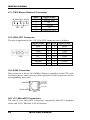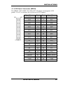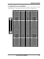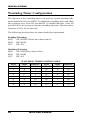
1
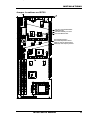
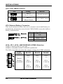
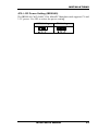
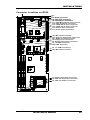
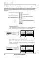
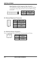
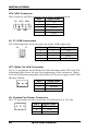
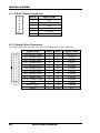
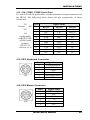
IB700
Full-Size Socket 370 CPU Card
With Optional VGA/LAN/SCSI
U S E R ’S M A N U A L
Version 1.0B
Acknowledgments
Award is a registered trademark of Award Software International,
Inc.
PS/2 is a trademark of International Business Machines
Corporation.
Intel and Celeron are registered trademarks of Intel Corporation.
Microsoft Windows is a registered trademark of Microsoft
Corporation.
Winbond is a registered trademark of Winbond Electronics
Corporation.
All other product names or trademarks are properties of their
respective owners.
ii
IB700 User’s Manual
Table of Contents
Introduction ..................................................................... 1
Product Description ........................................................1
Checklist ........................................................................2
Specifications .................................................................3
Board Dimensions...........................................................4
Installations...................................................................... 5
Installing the CPU...........................................................6
MicroPCI Daughter Card Installation ...............................6
Installing the Memory (DIMM)........................................7
Setting the Jumpers.........................................................8
Connectors on IB700 .................................................... 14
Watchdog Timer Configuration ...................................... 28
IB700 User’s Manual
iii
This page was intentionally left blank.
iv
IB700 User’s Manual
INTRODUCTION
Introduction
Product Description
IB700 is a high-performance flexible CPU card that comes with two builtin MicroPCI Sockets that supports MicroPCI daughter cards with VGA,
VGA/LAN, Ethernet (LAN), and SCSI functions. It is based on the Intel
440BX AGPset and features a Socket 370 architecture that supports Intel
Celeron and Coppermine processors using 66MHz and 100MHz front side
bus respectively.
System memory is provided by three DIMM sockets that accommodate
up to 768MB SDRAM. The Award BIOS facilitates easy system
configuration and peripheral setup. Other advanced features include
DiskOnChip flash disk support, watchdog timer, USB and IrDA interface.
DiskOnChip flash disks are storage devices that has no moving parts and
emulates FDD/HDD with Flash/RAM/ROM offering reliable
data/program storage and long life span. They are reliable and suitable for
industrial or other harsh environments characterized by motion, shock,
vibration, adverse temperature, dust and humidity. Other features include
faster data access, longer MTBF, lower power consumption, cost
effective for small capacity and small form factor.
The IB700 CPU card is designed with all components placed on a single
side, thus, offering stable performance in a harsh industrial environment.
IB700 User’s Manual
1
INTRODUCTION
Checklist
Your IB700 package should include the items listed below.
• The IB700 Industrial CPU Card
• This User’s Manual
• 1 IDE Ribbon Cable
• 1 Floppy Ribbon Connector
• 2 Serial Port Ribbon Cable and 1 Parallel Port Attached to a
Mounting Bracket
• 1 CD containing the following:
• Intel PCI IDE Driver and Flash Memory Utility
• CHIPS C&T 69000 VGA Drivers
• Ethernet Drivers
• Initio Inic1060 Ultra2 SCSI Drivers
2
IB700 User’s Manual
INTRODUCTION
Specifications
Processor
Supported
Chipset
BIOS
Socket 370 support Intel Celeron / Coppermine,
300MHz~850MHz, 66MHz/100MHz Bus Speed
SSD Interface
Other Features
Form Factor
Dimensions
Power
Requirements
Support M-Systems 2MB~144MB DiskOnChip flash disk
Intel 440BX AGPset
Award BIOS
Supports ACPI, DMI, PnP
3x DIMM sockets support up to 768MB capacity
System Memory
ECC supported
Multi I/O Chipset Winbond W83977TF (keyboard controller is built-in)
1x FDD (up to 2.88MB, 3 Mode, LS120)
I/O Features
1x Parallel Port (EPP, ECP Port)
2x Serial Ports (1x RS232 and 1x RS232/422/485)
1x IrDA TX/RX Headers
Bus Master IDE 2x IDE interfaces for up to 4 devices; supports PIO Mode 3/4
or Ultra DMA/33 IDE HDD, and ATAPI CD-ROM
Using IBD69 MicroPCI VGA card or IBD99 MicroPCI
VGA (option)
VGA/LAN Combo card that features:
CHIPS 69000 PCI VGA accelerator
CRT & LCD panel support
2MB integrated memory
Ethernet (option) Using IBD59 MicroPCI LAN card or IBD99 MicroPCI
VGA/LAN Combo card that features:
Intel 82559 Fast Ethernet controller
10/100Mbps data transfer speeds
WakeOnLAN support
Using IBD60 MicroPCI LAN SCSI card featuring:
SCSI (option)
Initio Inic1060 Ultra 2 SCSI controller
Built-in Ultra2 SCSI connector
Winbond W83781D IC
Hardware
Monitors CPU/system temperature and voltages
Monitoring
Watchdog timer, ISA high drive, PICMG compliance
Full Size
338mm x 122mm (13.3” x 4.8”)
+5V : 12A (max)
+/-12V : 200mA (max)
IB700 User’s Manual
3
INTRODUCTION
Board Dimensions
4
IB700 User’s Manual
INSTALLATIONS
Installations
This section provides information on how to use the jumpers and
connectors on the IB700 in order to set up a workable system. The topics
covered are:
Installing the CPU...........................................................6
MicroPCI Daughter Card Installation ...............................6
Installing the Memory (DIMM)........................................7
Setting the Jumpers.........................................................8
Connectors on IB700 .................................................... 14
Watchdog Timer Configuration ...................................... 28
IB700 User’s Manual
5
INSTALLATIONS
Installing the CPU
The IB700 CPU card supports a Socket 370 processor socket for Intel
Celeron/Coppermine processors.
The Socket 370 processor socket comes with a lever to secure the
processor. Raise this lever to about a 90° angle to allow the insertion of the
processor. Place the processor into the socket by making sure the notch
on the corner of the CPU corresponds with the notch on the inside of the
socket. Once the processor has slide into the socket, return the lever to
the lock position. After you have installed the processor into the socket,
check if the jumpers for the CPU type and speed are correct.
NOTE: Ensure that the CPU heat sink and the CPU top surface are in
total contact to avoid CPU overheating problem that would
cause your system to hang or be unstable.
MicroPCI Daughter Card Installation
The IB700 CPU card is integrated with two MicroPCI sockets that use
SO-DIMM 144-pin connectors. These sockets can accommodate the
VGA, Ethernet or SCSI MicroPCI daughter cards.
To insert a MicroPCI daughter card, position it at about 30° (Figure 1)
to the PCB and gently push it into the MicroPCI socket. Once inserted,
slowly press the card towards the PCB until it locks on both sides to the
clips of the connector (Figure 2). Screw the card to the PCB to secure the
installation.
Figure 1.
Figure 1.
6
Figure 2.
Figure 2.
IB700 User’s Manual
INSTALLATIONS
Installing the Memory (DIMM)
The IB700 CPU Card supports three 168-pin DIMM socket for a maximum
total memory of 768MB in SDRAM type. The memory module capacities
supported are 32MB, 64MB, 128MB and 256MB.
Installing and Removing DIMMs
To install the DIMM, locate the memory slot on the CPU card and perform
the following steps:
1. Hold the DIMM so that the two keys of the DIMM align with those on
the memory slot.
2. Gently push the DIMM in an upright position until the clips of the slot
close to hold the DIMM in place when the DIMM touches the bottom
of the slot.
3. To remove the DIMM, press the clips with both hands.
Lock
DIMM
Lock
Lock
Lock
Top View of DIMM Socket
IB700 User’s Manual
7
INSTALLATIONS
Setting the Jumpers
Jumpers are used on IB700 to select various settings and features
according to your needs and applications. Contact your supplier if you
have doubts about the best configuration for your needs. The following
lists the connectors on IB700 and their respective functions.
Jumper Locations on IB700......................................................................9
DSW1 (3): CPU Bus Speed Selector.....................................................10
DSW1 (5-8): CPU Frequency Selector..................................................10
JP3: Onboard LAN Enable/Disable (IBD99)........................................11
JP4: Onboard C&T VGA Enable/Disable (IBD99) ..............................11
JP5: Watchdog Selection .......................................................................11
JP6: DiskOnChip Address Select..........................................................11
JP8: Clear CMOS Content ......................................................................12
JP9: External Battery Connector............................................................12
JP10, JP11, JP12: RS232/422/485 (COM2) Selection ...........................12
JP2: LCD Power Setting (IBD99/69)......................................................13
The following conventions are used in this section:
o f f off on on
Pin 1-2
Short/Closed
↓ ↓ ↑ ↑
8
IB700 User’s Manual
S
INSTALLATIONS
I
Jumper Locations on IB700
D
JP10, JP11, JP12: RS232/422/485
(COM2) Selection
JP9: External Battery Connector
JP8: Clear CMOS Content
JP5: Watchdog Selection
JP6: DiskOnChip Address Select
DSW1 (3): CPU Bus Speed Selector
DSW1 (5-8): CPU Frequency Selector
IB700 User’s Manual
9
INSTALLATIONS
DSW1 (3): CPU Bus Speed Selector
Bus Speed
SW1 (3)
Switch
Setting
100MHz
off
66MHz
on
DSW1 (5-8): CPU Frequency Selector
The table below shows the correct setting to match the CPU frequency.
Frequency
Multiplier
CPU
Frequency
(66MHz)
CPU
Frequency
(100MHz)
4.5X
300MHz
450MHz
SW1(5-8)
xx xx xx xx off on off on
5X
333MHz
500MHz
xx xx xx xx off off on on
5.5X
366MHz
550MHz
xx xx xx xx off off off on
6X
400MHz
600MHz
xx xx xx xx on on on off
6.5X
433MHz
650MHz
xx xx xx xx on on off off
7X
466MHz
700MHz
xx xx xx xx on off on off
7.5X
500MHz
750MHz
xx xx xx xx on off off off
8X
533MHz
800MHz
xx xx xx xx off on on off
*IB700 BIOS can detect 850MHz CPU and no switch setting is required.
10
IB700 User’s Manual
INSTALLATIONS
JP3: Onboard LAN Enable/Disable (IBD99)
JP3
Setting
LAN Function
Pin 1-2
Short/Closed
Enabled
Pin 2-3
Short/Closed
Disabled
JP4: Onboard C&T VGA Enable/Disable (IBD99)
JP4
Setting
VGA Function
Pin 1-2
Short/Closed
Enabled
Pin 2-3
Short/Closed
Disabled
JP5: Watchdog Selection
JP5
Setting
Function
Pin 1-2
Short/Closed
Reset
Pin 2-3
Short/Closed
NMI
JP6: DiskOnChip Address Select
JP6
Address
D0000-D7FFF
D8000-DFFFF (default)
IB700 User’s Manual
11
INSTALLATIONS
JP8: Clear CMOS Content
JP8
Setting
Function
Pin 1-2
Short/Closed
Normal Operation
Pin 2-3
Short/Closed
Clear CMOS Content
JP9: External Battery Connector
This 4-pin connector allows the user to connect an external battery to
maintain the information stored in the CMOS RAM in case the built-in
battery malfunctions.
Pin #
1
2
3
4
Signal Name
Vcc
N.C.
Battery GND
Ground
JP10, JP11, JP12 : RS232/422/485 (COM2) Selection
COM1 is fixed for RS-232 use only.
COM2 is selectable for RS232, RS-422 and RS-485.
The following table describes the jumper settings for COM2 selection.
COM2
Function
Jumper
Setting
(pin closed)
12
RS-232
RS-422
RS-485
JP10:
1-2
JP10:
3-4
JP10:
5-6
JP11:
3-5 & 4-6
JP11:
1-3 & 2-4
JP11:
1-3 & 2-4
JP12:
3-5 & 4-6
JP12:
1-3 & 2-4
JP12:
1-3 & 2-4
IB700 User’s Manual
INSTALLATIONS
JP2: LCD Power Setting (IBD99/69)
The IBD99/69 C&T 69000 VGA MicroPCI daughter card supports 5V and
3.3V power. Use JP2 to select the power setting.
3.3V Setting
5V Setting
IB700 User’s Manual
13
INSTALLATIONS
[
Connectors on IB700
The connectors on IB700 allows you to connect external devices such as
keyboard, floppy disk drives, hard disk drives, printers, etc. The following
table lists the connectors on IB700 and their respective functions.
Connector Locations on IB700..............................................................15
J1: System Function Connector............................................................16
J2: External Keyboard Connector..........................................................18
J3: CPU Fan Power Connector...............................................................18
J4, J5: EIDE Connectors..........................................................................19
JP4: IrDA Connector...............................................................................20
J6, J7: USB Connectors...........................................................................20
JP7: Wake On LAN Connector..............................................................20
J8: System Fan Power Connector..........................................................20
J9: Floppy Drive Connector...................................................................21
J10: External ATX Power Connector....................................................21
J11: P8 AT Power Connector.................................................................22
J12: Parallel Port Connector...................................................................22
J13, J14: COM1, COM2 Serial Port ........................................................23
J15: PS/2 Keyboard Connector..............................................................23
J16: PS/2 Mouse Connector...................................................................23
J17: PS/2 Mouse External Connector....................................................24
J18: VGA CRT Connector.......................................................................24
J19: RJ45 Connector................................................................................24
J20, J21: MicroPCI Connectors..............................................................24
J1: LCD Panel Connector (IBD69).........................................................25
Flat Panel Display Interface Pin Descriptions.....................................26
JP1: WakeOnLAN Connector (IBD59).................................................26
J1: Ultra2 SCSI Connector (IBD60) .......................................................27
14
IB700 User’s Manual
INSTALLATIONS
Connector Locations on IB700
J19: RJ45 Connector
J18: VGA CRT Connector
J16: PS/2 Mouse Connector
PS/2 Mouse External Connector
PS/2 Keyboard Connector
COM2 Serial Port Connector
COM1 Serial Port Connector
Parallel Port Connector
P8 AT Power Connector
D
J17:
J15:
J14:
J13:
J12:
J11:
J21: MicroPCI Connector
J10: External ATX Power Connector
JP7: Wake On LAN Connector
J9: Floppy Drive Connector
J8: System Fan Power Connector
J4, J5: EIDE Connector
JP4: IrDA Connector
I
J6, J7: USB Connectors
J20: MicroPCI Connector
K
S
J1: System Function Connector
J2: External Keyboard Connector
J3: CPU Fan Power Connector
IB700 User’s Manual
15
INSTALLATIONS
J1: System Function Connector
J1 provides connectors for system indicators that provides light
indication of the computer activities and switches to change the computer
status. J1 is a 20-pin header that provides interfaces for the following
functions.
Hard Disk Drive LED
Reset Switch
Turbo LED Connector
ATX Power On Switch
SMI / Hardware Switch
Power LED and Keylock
Speaker
Speaker: Pins 1 - 4
This connector provides an interface to a speaker for audio
tone generation. An 8-ohm speaker is recommended.
Pin #
1
2
3
4
Signal Name
Speaker out
No connect
Ground
+5V
Power LED and Keylock: Pins 11 - 15
The power LED indicates the status of the main power
switch. The keylock switch, when closed, will disable the
keyboard function.
Pin #
11
12
13
14
15
16
IB700 User’s Manual
Signal Name
Power LED
No connect
Ground
Keylock
Ground
INSTALLATIONS
SMI/Hardware Switch: Pins 6 and 16
This connector supports the "Green Switch" on the control
panel, which, when pressed, will force the system into the
power-saving mode immediately.
Pin #
6
16
Signal Name
Sleep
Ground
ATX Power ON Switch: Pins 7 and 17
This 2-pin connector is an “ATX Power Supply On/Off
Switch” on the system that connects to the power switch on
the case. When pressed, the power switch will force the
system to power on. When pressed again, it will force the
system to power off.
Turbo LED Connector: Pins 8 and 18
There is no turbo/deturbo function on the CPU card. The
Turbo LED on the control panel will always be On when
attached to this connector.
Pin #
8
18
Signal Name
5V
Ground
Reset Switch: Pins 9 and 19
The reset switch allows the user to reset the system without
turning the main power switch off and then on again.
Orientation is not required when making a connection to this
header.
IB700 User’s Manual
17
INSTALLATIONS
Hard Disk Drive LED Connector: Pins 10 and 20
This connector connects to the hard drive activity LED on
control panel. This LED will flash when the HDD is being
accessed.
Pin #
10
20
Signal Name
Ground
5V
J2: External Keyboard Connector
1
5
J2
Pin #
1
2
3
4
5
Signal Name
Keyboard clock
Keyboard data
NC
GND
Vcc
J3: CPU Fan Power Connector
J3 is a 3-pin header for the CPU fan. The fan must be a 12V fan.
1 2 3
18
Pin #
1
2
3
Signal Name
Rotation
+12V
Ground
IB700 User’s Manual
INSTALLATIONS
J4, J5: EIDE Connectors
J5
J4
J5: Primary IDE Connector
Signal Name
Pin #
Reset IDE
1
Host data 7
3
Host data 6
5
Host data 5
7
Host data 4
9
Host data 3
11
Host data 2
13
Host data 1
15
Host data 0
17
Ground
19
DRQ0
21
Host IOW
23
Host IOR
25
IOCHRDY
27
DACK0
29
IRQ14
31
Address 1
33
Address 0
35
Chip select 0
37
Activity
39
Pin #
2
4
6
8
10
12
14
16
18
20
22
24
26
28
30
32
34
36
38
40
Signal Name
Ground
Host data 8
Host data 9
Host data 10
Host data 11
Host data 12
Host data 13
Host data 14
Host data 15
Key
Ground
Ground
Ground
Host ALE
Ground
No connect
No connect
Address 2
Chip select 1
Ground
J4: Secondary IDE Connector
Signal Name
Pin #
Pin #
Reset IDE
1
2
Host data 7
3
4
Host data 6
5
6
Host data 5
7
8
Host data 4
9
10
Host data 3
11
12
Host data 2
13
14
Host data 1
15
16
Host data 0
17
18
Ground
19
20
DRQ1
21
22
Host IOW
23
24
Host IOR
25
26
IOCHRDY
27
28
DACK1
29
30
IRQ15
31
32
Address 1
33
34
Address 0
35
36
Chip select 0
37
38
Activity
39
40
Signal Name
Ground
Host data 8
Host data 9
Host data 10
Host data 11
Host data 12
Host data 13
Host data 14
Host data 15
Key
Ground
Ground
Ground
Host ALE
Ground
No connect
No connect
Address 2
Chip select 1
Ground
IB700 User’s Manual
19
INSTALLATIONS
JP4: IrDA Connector
JP4 is used for an IrDA connector for wireless communication.
Pin #
Signal Name
+5V IRTX IRRX
1
+5V
2
No connect
3
Ir TX
N.C. GND
4
Ground
5
Ir RX
J6, J7: USB Connectors
The following table shows the pin outs of the USB connectors.
J6
1
2
3
4
J7
USB
1
2
3
4
J6 Pin #
1
2
3
4
J7 Pin #
1
2
3
4
Signal Name
Vcc
USBUSB+
Ground
JP7: Wake On LAN Connector
JP7 is a 3-pin header for the Wake On LAN function on the CPU card. The
following table shows the pin out assignments of this connector. Wake
On LAN will function properly only with an ATX power supply with 5VSB
that has 200mA.
1 2 3
Pin #
1
2
3
Signal Name
+5VSB
Ground
Wake on LAN
J8: System Fan Power Connector
J8 is a 3-pin header for the system fan. The fan must be a 12V fan.
1 2 3
20
Pin #
1
2
3
Signal Name
Rotation
+12V
Ground
IB700 User’s Manual
INSTALLATIONS
J9: Floppy Drive Connector
J9 is a 34-pin header and will support up to 2.88MB floppy drives.
J9
Signal Name
Ground
Ground
Ground
Ground
Ground
Ground
Ground
Ground
Ground
Ground
Ground
Ground
Ground
Ground
Ground
Ground
Ground
Pin #
1
3
5
7
9
11
13
15
17
19
21
23
25
27
29
31
33
Pin #
2
4
6
8
10
12
14
16
18
20
22
24
26
28
30
32
34
Signal Name
RM/LC
No connect
No connect
Index
Motor enable 0
Drive select 1
Drive select 0
Motor enable 1
Direction
Step
Write data
Write gate
Track 00
Write protect
Read data
Side 1 select
Diskette change
J10: External ATX Power Connector
1 2 3
Pin #
1
2
3
Signal Name
5VSB (Standby +5V)
PS-ON (soft on/of)
Ground
IB700 User’s Manual
21
INSTALLATIONS
J11: P8 AT Power Connector
1
6
J11
Pin #
1
2
3
4
5
6
Signal Name
N.C.
+5V
+12V
-12V
Ground
Ground
J12: Parallel Port Connector
The following table describes the pin out assignments of this connector.
J12
22
Signal Name
Line printer strobe
PD0, parallel data 0
PD1, parallel data 1
PD2, parallel data 2
PD3, parallel data 3
PD4, parallel data 4
PD5, parallel data 5
PD6, parallel data 6
PD7, parallel data 7
ACK, acknowledge
Busy
Paper empty
Select
Pin #
1
2
3
4
5
6
7
8
9
10
11
12
13
Pin #
14
15
16
17
18
19
20
21
22
23
24
25
N/A
IB700 User’s Manual
Signal Name
AutoFeed
Error
Initialize
Select
Ground
Ground
Ground
Ground
Ground
Ground
Ground
Ground
N/A
INSTALLATIONS
J13, J14: COM1, COM2 Serial Port
J13 and J14, both 10-pin headers, are the onboard serial port connectors of
the IB700. The following table shows the pin assignments of these
connectors.
J13
Pin #
fixed as
RS232
1
J14
configurable
as RS-232/ RS422/485 with
jumpers
JP10/11/12
(refer to p.12)
2
3
4
5
6
7
8
9
10
Signal Name
RS-232
DCD
RX
TX
DTR
GND
DSR
RTS
CTS
RI
NC
RS-422
TXTX+
RX+
RXGND
RTSRTS+
CTS+
CTSNC
RS-485
DATADATA+
NC
NC
GND
NC
NC
NC
NC
NC
J15: PS/2 Keyboard Connector
J15
Pin #
1
2
3
4
5
6
Signal Name
Keyboard data
N.C.
GND
5V
Keyboard clock
N.C.
J16: PS/2 Mouse Connector
J16
Pin #
1
2
3
4
5
6
Signal Name
Mouse data
N.C.
N.C.
5V
Mouse Clock
N.C.
IB700 User’s Manual
23
INSTALLATIONS
J17: PS/2 Mouse External Connector
M. Data Gnd M. Clk
N.C. 5V
Pin #
1
2
3
4
5
Signal Name
Mouse data
N.C.
Ground
5V
Mouse Clock
J18: VGA CRT Connector
The pin assignments of the J18 VGA CRT connector are as follows:
J18
Signal Name
Red
Blue
GND
GND
N.C.
N.C.
HSYNC
NC
Pin
1
3
5
7
9
11
13
15
Pin
2
4
6
8
10
12
14
Signal Name
Green
N.C.
GND
GND
GND
N.C.
VSYNC
J19: RJ45 Connector
This connector is for the 10/100Mbps Ethernet capability of the CPU card.
The figure below shows the pin out assignments of this connector and its
corresponding input jack.
TD+(pin#1)
TD-(pin#2)
RD+(pin#3)
Link LED
RD-(pin#6)
Active LED
J19
J20, J21: MicroPCI Connectors
J20 and J21 are MicroPCI connectors supporting MicroPCI daughter
cards with VGA, Ethernet or SCSI function.
24
IB700 User’s Manual
INSTALLATIONS
J1: LCD Panel Connector (IBD69)
The IBD69 C&T 69000 VGA MicroPCI daughter card supports LCD
panels. Use J1 to connect the system to an LCD panel.
50
2
49
J1
1
Signal Name
GND
P34
P35
P30
P29
P25
P24
P23
P16
P17
P19
P13
P15
P7
5V or 3.3V
P9
P4
P3
P2
M
SHFCLK
FPVDD
FPVEE
GND
+12V
Pin #
1
3
5
7
9
11
13
15
17
19
21
23
25
27
29
31
33
35
37
39
41
43
45
47
49
IB700 User’s Manual
Pin # Signal Name
2
P33
4
P31
6
P32
8
P28
10
P27
12
P26
14
P21
16
P22
18
P20
20
P18
22
P14
24
P12
26
P11
28
P10
30
5V or 3.3V
32
P8
34
P6
36
P5
38
P1
40
P0
42
ENABKL
44
FLM(V SYNC)
46
LP(H SYNC)
48
GND
50
+12V
25
INSTALLATIONS
Flat Panel Display Interface Pin Descriptions
Pin Name
P0
P1
P2
P3
P4
P5
P6
P7
P8
P9
P10
P11
P12
P13
P14
P15
P16
P17
P18
P19
P20
P21
P22
P23
P24
P25
P26
P27
P28
P29
P30
P31
P32
P33
P34
P35
SHFCLK
Pixels/Clk:
Mono Mono Mono Color Color Color Color Color
Color
Color
Color
Color
SS
DD
DD
TFT
TFT TFT TFT TFT+HR STN-SS STN-SS STN-DD STN-DD
8-bit 8-bit 16-bit 9/12/16 18/24 36-bit 18/24
8-bit
16-bit
8-bit
16-bit
24-bit
bit
bit
bit
(4bP)
(4bP)
(4bP)
(4bP)
D0
UD3 UD7
B0
B0
FB0 FB0
R1
R1
UR1
UR0
UR0
D1
UD2 UD6
B1
B1
FB1 FB1
B1
G1
UG1
UG0
UG0
D2
UD1 UD5
B2
B2
FB2 FB2
G2
B1
UB1
UB0
UB0
D3
UD0 UD4
B3
B3
FB3 FB3
B3
R2
UB2
UR1
LR0
D4
LD3 UD3
B4
B4
FB4 SB0
G4
G3
LR1
LR0
LG0
D5
LD2 UD2
G0
B5
FB5 SB1
R5
B2
LG1
LG0
LB0
D6
LD1 UD1
G1
B6 SB0 SB2
B5
R3
LB1
LB0
UR1
D7
LD0 UD0
G2
B7 SB1
B3
G3
LR2
LR1
UG1
LD7
G3
G0 SB2 FG0
B3
UG1
UB1
LD6
G4
G1 SB3 FG1
R4
UB1
LR1
LD5
G5
G2 SB4 FG2
G4
UR2
LG1
LD4
R0
G3 SB5 FG3
B4
UG2
LB1
LD3
R1
G4
FG0 SG0
R5
LG1
UR2
LD2
R2
G5
FG1 SG1
G5
LB1
UG2
LD1
R3
G6
FG2 SG2
B5
LR2
UB2
LD0
R4
G7
FG3 SG3
G6
LG2
LR2
R0
FG4 FR0
LG2
R1
FG5 FR1
LB2
R2 SG0
FR2
UR3
R3 SG1
FR3
UG3
R4 SG2 SR0
LR3
R5 SG3 SR1
LG3
R6 SG4 SR2
LB3
R7 SG5 SR3
FR0
FR1
FR2
FR3
FR4
FR5
SR0
SR1
SR2
SR3
SR4
SR5
SHFCL
K
SHFCL
K
SHFCL
K
SHFCLK
SHFCL
K
SHFCL
K
SHFCL
K
SHFCLK
SHFCLK
SHFCLK
SHFCLK
SHFCLK
8
8
16
1
1
2
2
2-2/3
5-1/3
2-2/3
5-1/3
8
P24
JP1: WakeOnLAN Connector (IBD59)
The IBD59 Intel 82559 LAN MicroPCI daughter card supports the JP1
WakeOnLAN connector. The following table shows the pin out
assignments of this connector. WakeOnLAN will function properly only
with an ATX power supply with 5VSB that has 800mA.
1 2 3
26
Pin #
1
2
3
Signal Name
+5VSB
Ground
Wake on LAN
IB700 User’s Manual
INSTALLATIONS
J1: Ultra2 SCSI Connector (IBD60)
The IBD60 Initio Inic1060 SCSI MicroPCI daughter card supports a 68-pin
SCSI connector. The table below shows its pin-out assignments.
J1
Signal Name
LVDP12
LVDP13
LVDP14
LVDP15
LVDPHP
LVDP0
LVDP1
LVDP2
LVDP3
LVDP4
LVDP5
LVDP6
LVDP7
LVDPLP
GROUND
DFFSENSE
GROUND
LVTRMPWR
LVTRMPWR
GROUND
LVATNP
GROUND
LVBSYP
LVACKP
LVRSTP
LVMSGP
LVSELP
LVCDP
LVREQP
LVIOP
LVDP8
LVDP9
LVDP10
LVDP11
Pin #
1
2
3
4
5
6
7
8
9
10
11
12
13
14
15
16
17
18
19
20
21
22
23
24
25
26
27
28
29
30
31
32
33
34
Pin #
35
36
37
38
39
40
41
42
43
44
45
46
47
48
49
50
51
52
53
54
55
56
57
58
59
60
61
62
63
64
65
66
67
68
IB700 User’s Manual
Signal Name
LVDM12
LVDM13
LVDM14
LVDM15
LVDPHM
LVDM0
LVDM1
LVDM2
LVDM3
LVDM4
LVDM5
LVDM6
LVDM7
LVDPLM
GROUND
LVEXT68
LVTRMPWR
LVTRMPWR
N.C.
GROUND
LVATNM
GROUND
LVBSYM
LVACKM
LVRSTM
LVMSGM
LVSELM
LVCDM
LVREQM
LVIOM
LVDM8
LVDM9
LVDM10
LVDM11
27
INSTALLATIONS
Watchdog Timer Configuration
The function of the watchdog timer is to reset the system automatically
and is defined at I/O port 0443H. To enable the watchdog timer and allow
the system to reset, write I/O port 0443H. To disable the timer, write I/O
port 0441H for the system to stop the watchdog function. The timer has a
tolerance of 20% for its intervals.
The following describes how the timer should be programmed.
Enabling Watchdog:
MOV AX, 000FH (Choose the values from 0)
MOV DX, 0443H
OUT
DX, AX
Disabling Watchdog
MOV AX, 00FH (Any value is fine.)
MOV DX, 0441H
OUT
DX, AX
WATCHDOG TIMER CONTROL TABLE
Level
1
2
3
4
5
6
7
8
28
Value
F
E
D
C
B
A
9
8
Time/sec
0
2
4
6
8
10
12
14
Level
9
10
11
12
13
14
15
16
IB700 User’s Manual
Value
7
6
5
4
3
2
1
0
Time/sec
16
18
20
22
24
26
28
30
APPENDIX
IB700 User’s Manual
29