1
The NCSU Design Kit for IC Fabrication through MOSIS
Toby Schaer
Andy Stanaski
Alan Glaser
Paul Franzon
September 16, 1998
Introduction
The North Carolina State University Cadence Design Kit (CDK) is a collection of technology les, custom
SKILL routines, parts libraries, and Diva rules les aimed at facilitating full-custom CMOS IC design through
MOSIS. The CDK is used at N.C. State University in both teaching and research, and it has been used to
fabricate working chips. This paper describes how to obtain and install the CDK, followed by a discussion
of the CDK's features. A summary of the CDK concludes the paper.
Installing the CDK
The CDK is very simple to install. It, as well as its patches, is distributed as a compressed tar le
that extracts into the $CDS ROOT/local directory. (Future versions will allow for more exibility as to
where the kit can be installed.) The CDK is distributed exclusively via the World Wide Web at the URL
http://www.ece.ncsu.edu/cadence/CDK.html. From this page there are links to:
view a brief listing of the CDK's features
download the latest complete CDK
download patches
Once the le is downloaded, copy it to $CDS ROOT, the root of your Cadence installation hierarchy. Uncompress and untar the kit, which will place its les under the local directory. Then run the setup.pl
Perl program, located in $CDS ROOT/local/bin, which copies startup les to the appropriate locations and
installs necessary symbolic links, or you can follow the instructions and perform these steps manually.
CDK Organization
This section provides a high-level overview of the contents of the CDK. All pathnames are relative to the
$CDS ROOT directory.
Documentation
CDK documentation is located in the local/doc tree. All custom forms have OpenBook screens accessible
through the form's \Help" button, and fairly-detailed documentation, in HTML format, describing the CDK
is included.
Technology Files and Diva Rules Files
The heart of the library creation is in the local/techfile directory. This directory contains the les which
dene the mask layers and their appearances and properties, as well as parameters used at library creation
time which set the value of lambda, the technology code, and the availability of process-dependent layers
(layers that are not common to all MOSIS processes). The example below shows the parameters for the HP
CMOS10QA process (which is 0:35m actual and 0:4m drawn):
; scmos-scn4m_subm-02.tf for HP CMOS10Q 0.35u
controls(
techParams(
( lambda
( technology
( metal3Available
( metal4Available
)
)
0.2 )
"SCN4M_SUBM" )
t )
t )
The structure of these les follows the ow described in the OpenBook section Technology File and Display
Resource File User Guide.
The Diva verication rules les are also located in the local/techfile directory. These are discussed later
in the section on Diva.
Technology Libraries
In local/lib, one technology library is provided for each MOSIS CMOS process. These libraries contain
layout parameterized cells (pcells) and provide users sitewide a set of reference libraries to which they can link
when creating their own project libraries. The technology libraries are generated by choosing the \Compile
Tech File" option during library creation, discussed in the \Design Framework" section below.
Standard Parts Libraries
Also in local/lib are the libraries NCSU Analog Parts, NCSU Digital Parts and NCSU Sheets 8ths, which
contain common analog and digital parts symbols, Verilog primitives, and example sheet borders. Originating
from the stock sample, analogLib and US 8ths libraries, they also include some other higher-level parts,
such as multiplexers and ip-ops. These libraries were created to consolidate the commonly-used parts in
a way that would allow us to add parts (e.g. multiplexers) and modify the parts with custom component
descriptor formats (CDFs) while keeping the original distribution libraries pristine.
These parts are technology-independent. SKILL callbacks triggered by the CDFs assign parameter values
(for example, minimum width and model name for transistors) to the parts only when they are placed in a
schematic. There is no layout data in these libraries.
Device Models
The local/models directory tree contains transistor model les. The CDK includes all the models we are
allowed to distribute (HSPICE level 13 and Spectre level 4), which are obtainable from the MOSIS web site;
for more detailed (HSPICE level 39) models contact MOSIS directly. The CDK sets the correct environment
variables so these models are found automatically when doing simulation through Analog Artist.
SKILL Code
The local/skill directory contains all the custom SKILL code | forms, menus, CDF callbacks, and pcell
denitions. This code, along with the Diva rules, provides the large majority of the CDK's added value.
There is too much to describe here; see local/skill/contents for a very brief description of each le.
RCS is used to implement revision control during development. However, only the most recent versions of
the les are distributed with the CDK.
Of special note is the le local/skill/globalData.il. As the name implies, it denes routines and
variables that are used by multiple parts of the CDK. One example is the NCSU techData array, which maps
a process to its technology code, process features and device sizes. One entry from this array is shown in
the SKILL fragment below:
NCSU_techData[ "HP 0.4u CMOS10QA (4 metal)" ] =
make_globalEntry(
?techFile
"scmos_scn4m_subm_02.tf"
?techLib
"hp10_TechLib"
?mosisCode
"SCN4M_SUBM"
?lambda
"0.2"
?minL
0.4
?minW
0.6
?gridRes
0.1
?submicronRules
t
?fetModelPrefix
"hp10"
)
The NCSU techData array is accessed by the library creation routines, Diva rules les and CDF callbacks.
Miscellaneous
There are also many les that don't t into any of the above categories, such as setup les (e.g., cdsenv)
that get read at startup time and a le of bindkeys (originally obtained from SourceLink) that give common
key bindings to both Composer and Virtuoso.
One useful program in particular is local/bin/xmesg, a simple Tcl/Tk script. Called from the site cdsinit
le, it pops up a window with a text message and a dismiss button. It's good for displaying short messages
that all users need to see at least once.
CDK Functionality
The CDK provides customizations for the Design Framework, Composer, Analog Artist, Verilog, Virtuoso
and Diva. This section describes the highlights of these customizations by tool.
Design Framework
As of this writing, MOSIS provides access to seven CMOS processes, with at least one more imminent.
Additionally, some of the individual processes have options associated with them. For example, when using
the HP CMOS14TB process MOSIS asks that the designer specify if two or three metals are used, and if
the linear capacitor well implant is to be used. For most new users, especially undergraduates, this can be
confusing. The CDK attempts to hide some of this detail by greatly simplifying library creation, as shown
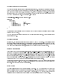
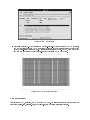
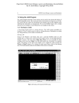
in Fig. 1.
Figure 1: Library Creation Form
The user rst types the name and directory of the new library. If the library is to include mask data
(i.e., layout), the user also chooses the appropriate process by name rather than by technology code. As
mentioned above, the CDK includes a technology library for each MOSIS CMOS process; by simply clicking
the appropriate button, the user either attaches the new library to one of these pre-existing technology
libraries or compiles the new library as its own technology library.
The selection of a given process allows access to only the mask layers available in that process. For example,
layouts done in HP's four-metal process CMOS10QA can use metal 4, while layouts done in HP's triplemetal CMOS14TB cannot. By making extensive use of xxxAvailable variables (where xxx is replaced by a
layername, as previously shown in the example controls class) only layers that actually exist in the library's
process are dened in the library's technology les.
After the library is created, the CDK creates links in the library's directory to the sitewide Diva rules les.
In a similar vein, the CDK replaces the stock form for attaching a technology library to a design library with
one that refers to the MOSIS CMOS processes by name.
Composer (schematic entry)
Already mentioned are the NCSU Analog Parts and NCSU Digital Parts libraries, which contain common
parts | e.g., logic gates, transistors, and RLC components | used for schematic capture and simulations.
One way these parts assist in schematic entry is through their CDFs, which mainly aect the transistors.
These CDFs:
enforce gridding; i.e., transistor widths and lengths must be a multiple of one-half lambda
enforce minimum transistor widths and lengths
automatically select the correct SPICE model based on the library's technology
use a simple heuristic to estimate the source and drain areas and perimeters
set properties so that the user can take advantage of the technology library's pcells when creating a
layout with DLE
Back annotation from layout is not supported at this time but is on the todo list.
Analog Artist (circuit simulation)
Circuit simulation is done through Analog Artist. There are relatively few customizations with respect to
this tool. As noted previously, the CDK includes several directories containing transistor models, and the
CDK's startup les set the necessary variables so Artist can nd these directories.
Verilog (digital simulation)
To assist digital simulations we provide Verilog primitives with the logic gates in the NCSU Digital Parts
library. Our Verilog hierarchy of views uses \functional" parts as leaf nodes, i.e. logic gates, and \behavioral"
parts as more abstract blocks. The simulation setup le simrc has been set up to netlist Verilog with this
hierarchy.
Virtuoso (mask design)
This section describes the CDK components aecting mask design with Virtuoso.
Mask Layers
All mask layers for all MOSIS SCMOS processes are supported, along with the optional layers that are not
common to all processes, such as Orbit's layers for NPN BJTs and HP's fourth metal. Adding support for a
new process is fairly straightforward (especially if the process does not introduce any new mask layers) and
is described in the CDK documentation. NCSU also releases patches to bring existing CDK installations
up-to-date as new MOSIS processes are announced.
In the local/doc directory of the CDK is the le layerInfo.html, which lists the Cadence layer name,
a description, the GDSII number and CIF abbreviation of all SCMOS layers as well as the process(es) for
which they are valid.
As discussed above, the CDK eliminates the temptation to use layers which do not exist in the technology
used by a design library by not dening those layers in the library when it is created.
Parameterized Cells
Parameterized cells are a popular and powerful way to assist in full-custom layout by eliminating the need
to manually draw every polygon of common structures such as FETs and contacts. Included in each precompiled MOSIS technology library are pcells for the following constructs (where applicable):
NFET/PFET
N/P ohmic contact
metal1 { N/P diusion contact
metal1 { poly/poly2 contact
metal2 { metal1 contact
metal3 { metal2 contact
metal4 { metal3 contact
thin-oxide linear capacitor
The FET parameters include the number of poly gates (in either serial or parallel congurations) as well as
width and length. The contact pcell parameters are number of rows and columns; all contact pitches are the
minimum allowed by the library's technology. The thin-oxide capacitor, currently available only in the HP
CMOS14TB process, can be described by either total capacitance desired or by width and height.
All pcells are implemented in hand-written SKILL except for the capacitor, which was implemented with
the Virtuoso pcell editor.
As mentioned previously, transistors from the NCSU Analog Parts library are automatically set to use these
FET pcells when creating devices via DLE.
Other Functionality
The following are some of the miscellaneous features the CDK brings to Virtuoso:
Symbolic contacts are provided to allow path-stitching with the path tool.
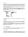
The label creation process is similar to Composer's, i.e., multiple labels can be typed into the form at
one time, and array notation is allowed, e.g., dataBus[7:0] will place eight separate labels. The label
creation form is shown in Fig. 2.
Figure 2: Label Creation Form
Elements (shapes and instances) can be selected and aligned to make their edges ush with a selected
object.
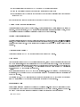
In the eye candy department, the user can import to layout JPEG images (handy for scanned-in logos
or signatures) and text strings in any available X Window font (quite useful for creating on-chip labels
and markers). These capabilities are provided by external programs, written in C and included with
the CDK in source form, accessible through the NCSU menu. The text import form is illustrated in
Fig. 3.
Figure 3: Text ! Layout Form
Especially useful for 3-D technologies such as Micro-Electro-Mechanical Systems (MEMS) processes,
and very educational for new CMOS designers, the user can draw an arbitrary cutline in a layout and
extract a cross-section across that line. This process is illustrated in Figs. 4 and 5, which are the top
and side view respectively of a capacitively-coupled contactless MEMS TBT switch.
Figure 4: MEMS TBT switch (top view)
Diva (verication)
All verication (DRC, extraction, and LVS) is done with Diva. The rules les are stored under the standard
lenames divaDRC.rul, divaEXT.rul, and divaLVS.rul in the local/techfile directory.
Figure 5: MEMS TBT switch (side view)
DRC
All rules from the MOSIS SCMOS User's Manual (rev. 7.2) are checked. The value of lambda is stored in
the globalData.il le as previously mentioned and used by Diva when performing DRC checks. In addition
to the SCMOS rules, a few extra rules are implemented that are not in the SCMOS manual but should be
followed anyway, such as not allowing p-type select inside cwell.
In the library MOSIS Layout Test is a layout, based on one provided by MOSIS, which consists of a group
of DRC-test structures which exercise every design rule.
Extraction
The following circuit elements can be extracted:
FETs
vertical NPNs
PN/NP diodes
poly-metal1/thin-ox/polycap capacitors
Parasitic capacitors can be extracted as well. A single SKILL variable sets the threshold below which
parasitic capacitances are ignored. Parasitic capacitance values are based on data published on the MOSIS
Web site.
Extraction of resistors and parasitic resistors is on the todo list.
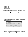
LVS
LVS is supported. Via a form accessible through the NCSU menu and shown in Fig. 6, the user can select
the desired LVS rules easily on a library-by-library basis.
Conclusions
This paper presented a summary and description of the North Carolina State University Cadence Design
Kit. An ongoing project, the CDK attempts to provide a user-friendly and ecient means to do full-custom
CMOS IC design through MOSIS. It includes pre-compiled technology libraries, Diva verication rules,
Figure 6: LVS Rules Selection Form
HSPICE/Spectre transistor models, layout pcells, and other various usability enhancements. The latest
version of and patches for the NCSU CDK are available at http://www.ece.ncsu.edu/cadence/CDK.html.
A PostScript version of this paper, as well as the slides presented at the 1998 Cadence User Group Conference,
can be obtained at http://www.ece.ncsu.edu/cadence/CUG1998.
Acknowledgements
The Diva DRC and extraction rules, as well as the base CMOS layers' appearances, are based on les
originally written by Jerey Gealow and Jen Lloyd, of MIT at the time. David Winick of NCSU wrote the
3-D cross-section extraction code. Text-to-layout conversion is done with the txt2layout package originally
written by Jerey Gealow and others.