1
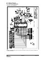
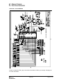
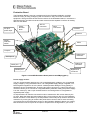
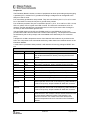
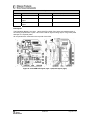
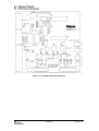
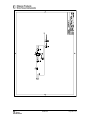
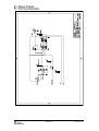
User Manual
Rev. 2.01
CC1010DK Development Kit
SWRU055
Table of contents
INTRODUCTION ....................................................................................................................... 3
EVALUATION MODULE........................................................................................................... 4
CIRCUIT DESCRIPTION .............................................................................................................. 4
PCB LAYOUT ........................................................................................................................... 5
SCHEMATIC, CC1010EM-433 .................................................................................................. 7
BILL OF MATERIALS, CC1010EM-433 ....................................................................................... 8
SCHEMATIC, CC1010EM-868 ................................................................................................ 11
BILL OF MATERIALS, CC1010EM-868 ..................................................................................... 12
EVALUATION BOARD ........................................................................................................... 15
POWER SUPPLY SECTION ........................................................................................................ 15
RS-232 INTERFACES .............................................................................................................. 16
PARALLEL INTERFACE ............................................................................................................. 16
JUMPERS ............................................................................................................................... 16
PERIPHERALS......................................................................................................................... 18
CONNECTORS ........................................................................................................................ 19
PCB LAYOUT ......................................................................................................................... 23
SCHEMATICS, CC1010EB...................................................................................................... 25
BILL OF MATERIALS, CC1010EB ............................................................................................ 30
USING THE DEVELOPMENT KIT.......................................................................................... 34
CC1010 RF EVALUATION USING SMARTRF® STUDIO............................................................... 34
SOFTWARE DEVELOPMENT USING THE IDE .............................................................................. 37
SERIAL CABLE PINOUT ....................................................................................................... 38
TROUBLESHOOTING ............................................................................................................ 39
IT DOESN’T WORK ................................................................................................................... 39
I CANNOT PROGRAM THE CC1010........................................................................................... 39
I CANNOT COMMUNICATE WITH THE CC1010 USING THE SERIAL PORT ....................................... 39
THE CC1010 DOESN’T OPERATE BELOW 3.1V (2.9±0.2V) ....................................................... 39
THE CC1010 CONSUMES MORE THAN THE RATED CURRENT IN POWER-DOWN MODE .................. 39
THE DEBUGGER CANNOT COMMUNICATE WITH THE CC1010 ..................................................... 39
DISCLAIMER .......................................................................................................................... 40
SWRU055
Page 2 of 40
Introduction
The CC1010 single chip RF transceiver and microcontroller provides a single-chip solution for
a wide range of applications. The CC1010DK development kit is designed to make it easy for
the user to evaluate the RF performance of the CC1010 and develop application software
very quickly.
The Development Kit includes an Evaluation Board and two Evaluation Modules. The
Evaluation Modules contain the CC1010 chip and associated support circuits. The Modules
can operate in a stand-alone fashion.
The Evaluation Board serves as a motherboard for the Evaluation Modules. The Evaluation
Board provides two serial ports, a parallel interface, buttons, LEDs, voltage regulator,
configuration jumpers and connectors to make it easy to interface the CC1010 with the IDE,
SmartRF® Studio and various test equipment.
This User Manual describes how to use the hardware part of the Development Kit. The
Chipcon-supplied software is documented in the IDE user manual, and the Keil µVision 2 C
compiler is documented in the Keil documentation. SmartRF® Studio is documented in its own
user manual.
The CC1010DK Development Kit includes what you need to evaluate the RF performance of
the CC1010, develop your own software for the CC1010 and can also be used to build a
prototype of your application. An evaluation version of the Keil µVision 2 C compiler is
included on the CD; this has a 2KB code size limitation.
Your SmartRF® CC1010DK Development Kit should contain the following items:
Kit contents
Item
Number of articles
Evaluation Board (CC1010EB)
1
Evaluation Module (CC1010EM)
2
Quick Start instructions
1
Chipcon CD
1
Antenna, 50Ω quarter-wave monopole, SMA male connector
2
SMA to BNC adapters
3
Parallel port cable
1
Serial null-modem cable
1
CC1010 sample kit
1
SWRU055
Page 3 of 40
Evaluation Module
The Evaluation Module contains the CC1010 chip, the needed external circuitry for operation,
pull-up resistors for all general I/O pins, test points and a temperature sensor. Not all
components are needed in an actual application. Please see the datasheet for a typical
application circuit.
The Evaluation Module is produced in two versions; the difference between them is the
frequency band of operation. One version is optimized for use at 433 MHz, the other for use
at 868 MHz and at 915 MHz. This covers the most used frequency bands, the 433 MHz band
in Europe and the US, the 868 MHz band in Europe, and the 902-928 MHz band in the US.
See application note AN001 for more information about applicable regulations. The operating
frequency band is marked on the PCB.
Circuit description
The CC1010 RF section includes all the necessary components for correct operation. An LC
filter is inserted between the CC1010 RF input/output and the antenna connector to reduce
harmonics. This LC filter is of the 3dB-equal ripple (Chebychev) low-pass type. The design
equations are:
1
⎛
⎞
⎟,
⎝ 1 − 0.1333 ⎠
ω C ≈ ω RF ⋅ ⎜
L=
35.6
ωC
,
C=
0.067
ωC
,
where ωC is the cut-off frequency and ωRF is the transmitted RF frequency. The filter is
designed for 50Ω termination impedances. If you wish to evaluate the CC1010 without an LC
filter, please remove capacitors C8 and C) and replace the L1 inductor with a 0Ω resistor.
The VCO inductor (L101) is located on the bottom side of the PCB, all other RF components
are on the top side.
The CC1010 is connected to both a 14.7456 MHz high-frequency crystal and a 32.768 kHz
low-frequency crystal. The high-frequency crystal is furnished with a trimmer capacitor to
adjust the initial frequency tolerance. An external signal can be applied at test pin TP1,
remember to remove the crystal before applying an external clock signal. The external clock
should have an amplitude of 1 – 3 V peak-to-peak.
Power can easily be applied to the board by using the TP3 and TP4 test points, or connecting
the power source to the adjoining bare copper areas. The TP2, TP5 and TP6 test points
provide easy access to the P0.0, P0.1 and P0.2 I/O pins, respectively.
All general-purpose I/O pins are furnished with pull-up resistors, ensuring that the pins do not
float if they are configured as inputs. An LM-61 temperature sensor from National
Semiconductor is also included on the board, and is connected to the AD1 pin. If this pin is to
be used for other purposes, the temperature sensor should be removed.
The Evaluation Module can be plugged into the Evaluation Board. 2 2x20 pin pin-row
connectors with 0.050-inch pitch are used for this purpose. Shorting the T1 and T2 pads
together for a short period will reset the CC1010.
SWRU055
Page 4 of 40
High-frequency
crystal
Trimmer
capacitor
32.768 kHz
crystal
Power
connections
Antenna
connector
CC1010
Temperature
sensor
Figure 1: CC1010EM Evaluation Module
PCB layout
The figure above shows the 1.0 revision of the PCB. Later revisions are similar, but have the
following additional features:
•
0-ohm series resistor between the temperature sensor and the AD1 bit of CC1010.
Instead of desoldering the temperature sensor if you wish to use AD1 for other
purposes, you can desolder the 0-ohm resistor.
•
0-ohm series resistor between temperature sensor and VDD. Instead of desoldering
the temperature sensor when measuring the power-down current of the CC1010, you
can desolder the 0-ohm resistor.
RF circuits operating at high frequencies are sensitive to the physical layout of the PCB.
Chipcon has carefully optimized the layout of the CC1010EM evaluation module, and we
recommend that you copy it when making your own PCB design.
The PCB is of a 4-layer type in order to provide a good ground plane as well as adequate
routing space. The laminate used is standard FR-4 board material. The PCB is 1.6mm thick,
with layer 1 on the top side, layers 2 and 3 are internal layers and layer 4 is on the bottom
side. Layers 1 and 4 are used for routing, while layer 2 is a ground plane and layer 3 is used
for power routing. All areas not utilized for routing are filled with copper connected to ground
to provide RF shielding. The ground planes on all layers are stitched together with closely
spaced vias.
To minimize LO leakage and allow space for decoupling capacitors close to the CC1010, the
VCO inductor (L101) is placed on the bottom side of the PCB. EMI beads for power-supply
filtering are also placed on the bottom side, together with the pull-up resistors. All other
components are placed on the top side of the PCB.
SWRU055
Page 5 of 40
Figure 2: CC1010EM PCB layout, layer 1 (left) and layer 3 (right)
Figure 3: CC1010EM PCB layout, layer 4 (left) and layer 2 (right, negative)
Figure 4: CC1010EM component placement, top side (left) and bottom side (right)
SWRU055
Page 6 of 40
Schematic, CC1010EM-433
Please note that the TEST_N pin should be connected to VDD in your design. See page 40
for more information.
SWRU055
Page 7 of 40
Bill of materials, CC1010EM-433
Bill of materials, CC1010EM-433
Reference
Description
Value
Part
C1
Capacitor, tantal
3.3uF
C_3U3_TAN_B
C4
Capacitor 0603
1nF, 5%
C_1N0_0603_X7R_J_50
C8
Capacitor 0603
12pF, 5%
C_12P_0603_NP0_J_50
C9
Capacitor 0603
12pF, 5%
C_12P_0603_NP0_J_50
C12
Capacitor 0603
6.8pF, ±0.25pF
C_6P8_0603_NP0_C_50
C13
Capacitor 0603
6.8pF, ±0.25pF
C_6P8_0603_NP0_C_50
C14
Capacitor 0603
15pF, 5%
C_15P_0603_NP0_K_50
C15
Capacitor 0603
15pF, 5%
C_15P_0603_NP0_K_50
C19
Capacitor 0603
33nF, 10%
C_33N_0603_X7R_K_25
C20
Capacitor 0603
220pF, 5%
C_220P_0603_NP0_G_50
C21
Capacitor 0603
33nF, 10%
C_33N_0603_X7R_K_25
C22
Capacitor 0603
150pF, 5%
C_150P_0603_NP0_G_50
C23
Capacitor 0603
general
C24
Capacitor 0603
150pF, 5%
C_150P_0603_NP0_J_50
C25
Capacitor 0603
33nF, 10%
C_33N_0603_X7R_K_25
C26
Capacitor 0603
150pF, 5%
C_150P_0603_NP0_J_50
C27
Capacitor 0603
33nF, 10%
C_33N_0603_X7R_K_25
C31
Capacitor 0603
10pF, 5%
C_10P_0603_NP0_J_50
C32
Capacitor 0603
1nF, 5%
C_1N0_0603_X7R_J_50
C34
Capacitor 0603
33nF, 10%
C_33N_0603_X7R_K_25
C35
Capacitor 0603
1nF, 10%
C_1N0_0603_X7R_K_50
C41
Capacitor 0603
6.8pF, ±0.25pF
C_6P8_0603_NP0_C_50
C42
Capacitor 0603
8.2pF, ±0.25pF
C_8P2_0603_NP0_C_50
C47
Capacitor 0603
33nF, 10%
C_33N_0603_X7R_K_25
CT1
Trimmer Capacitor
3-10pF
C_3-10P_TRIM_NP0
L1
Inductor 0805
15nH, 5%
L_15N_0805_J
L2
Resistor 0603
0Ω
R_0_0603
L3
Resistor 0603
0Ω
R_0_0603
L7
Resistor 0603
0Ω
R_0_0603
L8
Resistor 0603
0Ω
R_0_0603
L9
Resistor 0603
0Ω
R_0_0603
L10
Resistor 0603
0Ω
R_0_0603
Do not mount
SWRU055
Page 8 of 40
Bill of materials, CC1010EM-433
Reference
Description
Value
Part
L20
Resistor 0603
0Ω
R_0_0603
L21
Resistor 0603
0Ω
R_0_0603
L22
Resistor 0603
0Ω
R_0_0603
L32
Inductor 0805
68nH, 5%
L_68N_0805_J
L41
Inductor, 0805
6.2nH, 5%
L_6N2_0805_J
L101
Inductor, 0603
(KOA)
27nH, 5%
L_27N_0603_KL73, KOA
KL731JTE27NJ
P1
SMD pin-row
socket, .050 spacing
SMD_SOCKET_2X20, Samtec SFM120-02-S-D-A-K-TR
P2
SMD pin-row
socket, .050 spacing
SMD_SOCKET_2X20, Samtec SFM120-02-S-D-A-K-TR
P3
Surface-mount
SMA, straight
SMA_SMD
R1
Resistor 0603
47kΩ, 2%
R_47K_0603_G
R3
Resistor 0603
47kΩ, 2%
R_47K_0603_G
R4
Resistor 0603
47kΩ, 2%
R_47K_0603_G
R5
Resistor 0603
47kΩ, 2%
R_47K_0603_G
R6
Resistor 0603
47kΩ, 2%
R_47K_0603_G
R7
Resistor 0603
47kΩ, 2%
R_47K_0603_G
R8
Resistor 0603,
general
R9
Resistor 0603
47kΩ, 2%
R_47K_0603_G
R10
Resistor 0603
27kΩ, 2%
R_27K_0603_G
R11
Resistor 0603
47kΩ, 2%
R_47K_0603_G
R12
Resistor 0603
47kΩ, 2%
R_47K_0603_G
R13
Resistor 0603
47kΩ, 2%
R_47K_0603_G
R14
Resistor 0603
47kΩ, 2%
R_47K_0603_G
R15
Resistor 0603
47kΩ, 2%
R_47K_0603_G
R16
Resistor 0603
47kΩ, 2%
R_47K_0603_G
R17
Resistor 0603
47kΩ, 2%
R_47K_0603_G
R18
Resistor 0603
47kΩ, 2%
R_47K_0603_G
R19
Resistor 0603
47kΩ, 2%
R_47K_0603_G
R20
Resistor 0603
47kΩ, 2%
R_47K_0603_G
R21
Resistor 0603
47kΩ, 2%
R_47K_0603_G
R22
Resistor 0603
47kΩ, 2%
R_47K_0603_G
R23
Resistor 0603
47kΩ, 2%
R_47K_0603_G
Do Not Mount
SWRU055
Page 9 of 40
Bill of materials, CC1010EM-433
Reference
Description
Value
Part
R24
Resistor 0603
47kΩ, 2%
R_47K_0603_G
R25
Resistor 0603
47kΩ, 2%
R_47K_0603_G
R26
Resistor 0603
47kΩ, 2%
R_47K_0603_G
R27
Resistor 0603
47kΩ, 2%
R_47K_0603_G
R28
Resistor 0603
R29
Resistor 0603
47kΩ, 2%
R_47K_0603_G
R30
Resistor 0603
47kΩ, 2%
R_47K_0603_G
R31
Resistor 0603
47kΩ, 2%
R_47K_0603_G
R32
Resistor 0603
47kΩ, 2%
R_47K_0603_G
R33
Resistor 0603
47kΩ, 2%
R_47K_0603_G
R131
Resistor 0603
82kΩ, 1%
R_82K_0603_F
TP1
Testpoint
TESTPIN
TP2
Testpoint
TESTPIN
TP3
Testpoint
TESTPIN
TP4
Testpoint
TESTPIN
TP5
Testpoint
TESTPIN
TP6
Testpoint
TESTPIN
U1
Single-chip
transceiver and
microcontroller
CC1010
U2
Temperature
sensor, SOT23
LM61, National Semiconductor
LM61CIM3
X1
Crystal, HC-49-SMD
X 14.7456 MHz 10/10/10/16pF load
X2
Watch crystal,
plastic SMD
package
X 32.768 kHz 20/50/10/12pF load
Do not mount
SWRU055
Page 10 of 40
Schematic, CC1010EM-868
Please note that the TEST_N pin should be connected to VDD in your design. See page 40
for more information.
SWRU055
Page 11 of 40
Bill of materials, CC1010EM-868
Bill of materials, CC1010EM-868
Reference
Description
Value
Part
C1
Capacitor, tantal
3.3uF
C_3U3_TAN_B
C4
Capacitor 0603
1nF, 5%
C_1N0_0603_X7R_J_50
C8
Capacitor 0603
10pF, 5%
C_10P_0603_NP0_J_50
C9
Capacitor 0603
8.2pF, ±0.25pF
C_8P2_0603_NP0_C_50
C12
Capacitor 0603
6.8pF, ±0.25pF
C_6P8_0603_NP0_C_50
C13
Capacitor 0603
6.8pF, ±0.25pF
C_6P8_0603_NP0_C_50
C14
Capacitor 0603
15pF, 5%
C_15P_0603_NP0_J_50
C15
Capacitor 0603
15pF, 5%
C_15P_0603_NP0_J_50
C19
Capacitor 0603
33nF, 10%
C_33N_0603_X7R_K_25
C20
Capacitor 0603
220pF, 5%
C_220P_0603_NP0_G_50
C21
Capacitor 0603
33nF, 10%
C_33N_0603_X7R_K_25
C22
Capacitor 0603
22pF, 5%
C_22P_0603_NP0_J_50
C23
Capacitor 0603
150pF, 5%
C_150P_0603_NP0_J_50
C24
Capacitor 0603
150pF, 5%
C_150P_0603_NP0_J_50
C25
Capacitor 0603
33nF, 10%
C_33N_0603_X7R_K_25
C26
Capacitor 0603
12pF, 5%
C_12P_0603_NP0_J_50
C27
Capacitor 0603
33nF, 10%
C_33N_0603_X7R_K_25
C31
Capacitor 0603
8.2pF, ±0.25pF
C_8P2_0603_NP0_C_50
C32
Capacitor 0603
1nF, 5%
C_1N0_0603_X7R_J_50
C34
Capacitor 0603
33nF, 10%
C_33N_0603_X7R_K_25
C35
Capacitor 0603
1nF, 10%
C_1N0_0603_X7R_K_50
C41
Capacitor 0603,
general
C42
Capacitor 0603
10pF, 5%
C_10P_0603_NP0_J_50
C47
Capacitor 0603
33nF, 10%
C_33N_0603_X7R_K_25
CT1
Trimmer Capacitor
3-10pF
C_3-10P_TRIM_NP0
L1
Inductor 0805
3.3nH, ± 0.5nH
L_3N3_0805_D
L2
EMI Filter Bead
BLM18HG102SN1D, Murata
L3
EMI Filter Bead
BLM18HG102SN1D, Murata
L7
EMI Filter Bead
BLM18HG102SN1D, Murata
L8
Resistor 0603
0Ω
R_0_0603
L9
Resistor 0603
0Ω
R_0_0603
L10
Resistor 0603
0Ω
R_0_0603
L20
Resistor 0603
0Ω
R_0_0603
Do Not Mount
SWRU055
Page 12 of 40
Bill of materials, CC1010EM-868
Reference
Description
Value
Part
L21
Resistor 0603
0Ω
R_0_0603
L22
Resistor 0603
0Ω
R_0_0603
L32
Inductor 0805
12nH, 5%
L_12N_0805_J
L41
Inductor, 0805
2.5nH, 5%
L_2N5_0805_J
L101
Inductor, 0603
(KOA)
3.3nH, 5%
L_3N3_0603_KL73, KOA
KL731JTE3N3J
P1
SMD pin-row
socket, .050 spacing
SMD_SOCKET_2X20, Samtec SFM120-02-S-D-A-K-TR
P2
SMD pin-row
socket, .050 spacing
SMD_SOCKET_2X20, Samtec SFM120-02-S-D-A-K-TR
P3
Surface-mount
SMA, straight
SMA_SMD
R1
Resistor 0603
47kΩ, 2%
R_47K_0603_G
R3
Resistor 0603
47kΩ, 2%
R_47K_0603_G
R4
Resistor 0603
47kΩ, 2%
R_47K_0603_G
R5
Resistor 0603
47kΩ, 2%
R_47K_0603_G
R6
Resistor 0603
47kΩ, 2%
R_47K_0603_G
R7
Resistor 0603
47kΩ, 2%
R_47K_0603_G
R8
Resistor
0603,general
R9
Resistor 0603
47kΩ, 2%
R_47K_0603_G
R10
Resistor 0603
27kΩ, 2%
R_27K_0603_G
R11
Resistor 0603
47kΩ, 2%
R_47K_0603_G
R12
Resistor 0603
47kΩ, 2%
R_47K_0603_G
R13
Resistor 0603
47kΩ, 2%
R_47K_0603_G
R14
Resistor 0603
47kΩ, 2%
R_47K_0603_G
R15
Resistor 0603
47kΩ, 2%
R_47K_0603_G
R16
Resistor 0603
47kΩ, 2%
R_47K_0603_G
R17
Resistor 0603
47kΩ, 2%
R_47K_0603_G
R18
Resistor 0603
47kΩ, 2%
R_47K_0603_G
R19
Resistor 0603
47kΩ, 2%
R_47K_0603_G
R20
Resistor 0603
47kΩ, 2%
R_47K_0603_G
R21
Resistor 0603
47kΩ, 2%
R_47K_0603_G
R22
Resistor 0603
47kΩ, 2%
R_47K_0603_G
R23
Resistor 0603
47kΩ, 2%
R_47K_0603_G
R24
Resistor 0603
47kΩ, 2%
R_47K_0603_G
Do Not Mount
SWRU055
Page 13 of 40
Bill of materials, CC1010EM-868
Reference
Description
Value
Part
R25
Resistor 0603
47kΩ, 2%
R_47K_0603_G
R26
Resistor 0603
47kΩ, 2%
R_47K_0603_G
R27
Resistor 0603
47kΩ, 2%
R_47K_0603_G
R28
Resistor 0603
R29
Resistor 0603
47kΩ, 2%
R_47K_0603_G
R30
Resistor 0603
47kΩ, 2%
R_47K_0603_G
R31
Resistor 0603
47kΩ, 2%
R_47K_0603_G
R32
Resistor 0603
47kΩ, 2%
R_47K_0603_G
R33
Resistor 0603
47kΩ, 2%
R_47K_0603_G
R131
Resistor 0603
82kΩ, 1%
R_82K_0603_F
TP1
Testpoint
TESTPIN
TP2
Testpoint
TESTPIN
TP3
Testpoint
TESTPIN
TP4
Testpoint
TESTPIN
TP5
Testpoint
TESTPIN
TP6
Testpoint
TESTPIN
U1
Single-chip
transceiver and
microcontroller
CC1010
U2
Temperature
sensor, SOT23
LM61, National Semiconductor
LM61CIM3
X1
Crystal, HC-49-SMD
X 14.7456 MHz 10/10/10/16pF load
X2
Watch crystal,
plastic SMD
package
X 32.768 kHz 20/50/10/12pF load
Do not mount
SWRU055
Page 14 of 40
Evaluation Board
The Evaluation Board is used as a motherboard for the Evaluation Modules, providing
external circuitry for easy prototyping and connectors for easy connection to external
equipment. The figure below shows the first revision of the Evaluation Board; in revisions 3.0
and later the AD1 and AD2 connectors were removed, and a separate connector for analog
data out was added.
Power
terminal
block
DC jack
power input
SPI I/O
connector
SMA
connectors
Potmeter
Buttons
Power
selection
switch
LEDs
Jumpers
Digital I/O B
connector
Serial port 0
Analog I/O
connector
Serial port 1
Parallel port
Digital I/O A
connector
Figure 5: CC1010EB Evaluation Board (with CC1010EM plugged in)
Power supply section
You can choose between applying a 4-10V unregulated supply voltage or a 3.3V regulated
supply voltage by using the SPDT switch. If an unregulated supply voltage is applied, a onboard regulator supplies 3.3V to the board. A diode prevents damage if wrong polarity is
applied to the non-regulated input. There are two power connectors; a 3.5mm DC jack-type
connector allows you to connect an unregulated battery eliminator easily (the positive supply
is on the center pin), and a 5-pin terminal block for connecting either an unregulated or
regulated power supply.
An amperemeter can also be connected in order to measure the DC current drawn by the
CC1010. Note that these terminals measure all the current going to the CC1010 Evaluation
Module, therefore current drawn by the temperature sensor and pull-up resistors will also be
measured. If you are going to measure the power-down current of the CC1010 accurately,
you should remove the temperature sensor on the Evaluation Module (it draws over 100uA),
and set all the CC1010 I/O pins to be inputs or outputs set to the high state. If you are not
SWRU055
Page 15 of 40
going to measure the current, a short-circuit jumper must be connected between these two
terminals, otherwise the Evaluation Module will not be supplied with power.
4-10V
0V
3V
A
Iout
Figure 6: Power terminal block with amperemeter attached
On the PCB, all pins connected to regulated power are marked with VCC. On the schematics,
this net is called +3.3V. Power going to the Evaluation Module connector is named
+3.3V_RF.
RS-232 interfaces
The Evaluation Board provides two serial ports, Serial 0 and Serial 1. The serial ports are
configured as DTE (Data Terminal Equipment, in other words identical to a PC). Therefore, a
null-modem cable with data lines crossed must be used to connect these ports to a PC. A
level-conversion circuit is provided to convert the CMOS levels used by the CC1010 into RS232 compliant bipolar +5V/-5V signals. Note that this circuit contains a charge-pump power
supply that is quite noisy. When doing performance evaluation of the CC1010 RF section, we
recommend that you turn this circuit off by inserting the SER OFF strap.
Serial 0 implements the RTS/CTS handshaking pair, so that hardware handshaking may be
used on this port. These signals are available at pins P1.5 and P1.6. Serial 1 is primarily used
by the Keil debugger to communicate with the CC1010 when the debugger is running. Serial
1 does not implement hardware handshaking. A way to reset the CC1010 via this port is
provided; removing the SER RST jumper will disable this function.
Parallel interface
The Evaluation Board also provides a parallel interface for connection to a parallel port on a
PC. This interface is used to communicate with SmartRF® Studio and the CC1010 Flash
Programmer program. The parallel interface can be disconnected from the CC1010 I/O pins
by removing the PAR EN jumper. Removing the PAR PROG jumper will disable parallel
programming of the CC1010.
Jumpers
The jumpers are used to configure the Evaluation Board. The factory default settings are
shown below, please return to these settings if you are experiencing any problems.
SWRU055
Page 16 of 40
Figure 7 Default jumper settings
Jumpers
Name
Default
setting
Description
AD1 TEMP
Not
present
If present, connects the temperature sensor footprint on the
Evaluation Board to the AD1 pin of the CC1010. (Note: This
jumper does not control the temperature sensor located on the
Evaluation Module) In PCB revision 3.0 and later, this strap does
not exist. Neither does the footprint on the EB for the temperature
sensor.
AD0 POT
Present
If present, connects the RT1 potmeter to the AD0 pin of the
CC1010.
PAR PROG
Present
If present, enables programming of the CC1010 Flash memory via
the parallel interface.
POR ON
Present
If present, enables the internal power-on reset module of the
CC1010. When enabled, the supply voltage must be over 2.9V
±0.2V for the CC1010 to exit the reset condition.
TEST OFF
Present
This jumper should always be present.
SER RST
Present
If present, enables resetting the CC1010 via the SERIAL 1 serial
port.
PAR RST
Present
If present, enables resetting the CC1010 via the parallel interface.
SER OFF
Not
present
If present, disables the RS-232 interface circuitry. Because this
circuitry generates noise, we recommend disabling it when
sensitive RF measurements are performed. If the circuitry is
disabled, the serial ports cannot be used.
DIO ANA
Present
When present, enables adjustment of the DIO peak-to-peak signal
level using the DIO ATT potmeter when performing BER testing
using SmartRF® Studio. In PCB revision 3.0 and later, this strap
does not exist as analog data out has its own separate connector.
PAR EN
Present
When present, enables the parallel interface. If this is disabled,
communication with SmartRF® Studio or the CC1010 Flash
programmer is impossible.
SWRU055
Page 17 of 40
Peripherals
The Evaluation Board includes a number of peripherals to allow quick testing and prototyping.
A potmeter (RT1, marked “POT”) provides an analogue voltage that can be applied to the
AD0 pin of the CC1010.
Four momentary pushbuttons are provided. They are connected to pins P1.7, P3.2, P3.3 and
P2.4. The buttons connect the I/O pins to ground when pushed.
Four LEDs are provided. They are connected to pins P1.2, P1.3, P1.4 and P2.5. LED 1 is red,
LED 2 is yellow, LED 3 is green and LED 4 is blue. The LEDs are connected to VCC via
resistors, and the cathodes are connected to the CC1010 I/O pins via a buffer. Driving the
CC1010 pin low will therefore light the LED.
The two PWM outputs of the CC1010 (PWM2 at pin P3.4 and PWM3 at pin P3.5) are
provided with buffers and RC-filters with a 3-kHz cutoff frequency. The outputs from the filters
are buffered by rail-to-rail op-amps, and are available at the ANALOG pin-row connector
(P15).
A footprint for a LM61 temperature sensor from National Semiconductor is provided on the
PCB. This component is not mounted at the factory; rather there is an identical sensor on the
Evaluation Module.
A reset button is provided. When pushed, it will reset the CC1010 by pulling its RESET line
low.
Peripheral summary
Peripheral
CC1010 pin
Description
POT (RT1)
AD0
10kΩ Potmeter. Can apply a voltage between VCC and 0V.
Can be disconnected from AD0 by removing the AD0 POT
jumper.
Button 1
P1.7
Momentary pushbutton. When activated, pulls I/O line low.
Button 2
P3.2
Momentary pushbutton. When activated, pulls I/O line low.
Button 3
P3.3
Momentary pushbutton. When activated, pulls I/O line low.
Button 4
P2.4
Momentary pushbutton. When activated, pulls I/O line low.
LED 1
P1.2
Red LED. Buffered, lights up when I/O line is pulled low.
LED 2
P1.3
Yellow LED. Buffered, lights up when I/O line is pulled low.
LED 3
P1.4
Green LED. Buffered, lights up when I/O line is pulled low.
LED 4
P2.5
Blue LED. Buffered, lights up when I/O line is pulled low.
PWM 2 buffer
and filter
P3.4
PWM output is buffered by CMOS buffer, then low-pass
filtered (RC filter with 3 kHz cut-off frequency) and buffered by
a rail-to-rail op-amp. Output available at ANALOG connector.
PWM 3 buffer
and filter
P3.5
PWM output is buffered by CMOS buffer, then low-pass
filtered (RC filter with 3 kHz cut-off frequency) and buffered by
a rail-to-rail op-amp. Output available at ANALOG connector.
Temperature
sensor
AD1
Footprint for LM61CIM3 temperature sensor from National
Semiconductor. Not mounted. Can be disconnected from AD1
by removing the AD0 POT jumper. This footprint is not
present on revision 3.0 or later of the PCB. Note that an
identical temperature sensor is mounted on the Evaluation
Module.
SWRU055
Page 18 of 40
Connectors
The Evaluation Board is furnished with many connectors for easy access to signals.
The I/O A (P14) and I/O B (P16) 2x10 pin pin-row connectors bring out all the general digital
I/O pins of the CC1010. The pin-out is compatible with logic analyzer probes from Agilent.
Analog signals are brought out on the 2x5 pin ANALOG (P15) connector. All A/D inputs to the
CC1010 are available here, as well as buffered and filtered PWM outputs.
The SPI (P5) connector brings out all signals related to CC1010 Flash programming and
CC1010 SPI Master functionality.
The Evaluation Modules are plugged into sockets P1 and P2. These sockets are keyed, and
it is not possible to orient the module incorrectly. Make sure you have turned off all power to
the Evaluation Board before inserting or removing any Modules.
Several important signals have been brought out on SMA connectors for easy access.
AD2/RSSI/IF brings out the AD2/RSSI/IF pin on the CC1010. The AD1/REF connector is
connected to the AD1 pin on the CD1010. The DIO and DCLK pins are connected to the P0.1
and P0.2 pins on the CC1010. When using SmartRF® Studio, the CC1010 can “emulate” the
CC1000 for RF measurements. The recovered clock signal will then be available on the DIO
connector, and DIO will present received data in RX mode, and the user can apply data to
DIO in TX mode. The DIO ATT potmeter can be used to adjust the amplitude of the DIO
signal in TX mode when BER measurements are done. Please see the section on BER
testing in this manual for more information.
Some modifications have been made on PCB revisions 3.0 and later. The AD1/REF and
AD2/RSSI/IF SMA connectors have been removed (the signals are still available on the
ANALOG pin-row connector), and a separate analog data out connector has been added.
The identity of each pin is shown in the PCB silkscreen next to each pin. The tables below
provide further information.
If you make your own custom CC1010 PCB, we recommend including a connector similar to
the SPI connector on the CC1010EB. You can then connect the two connectors together with
a flat cable and use the CC1010EB to program flash and run the debugger. If you connect the
VCC pins together, make sure that you’ve thought out the power supply issues. The regulator
on the CC1010EB is not dimensioned for delivering large currents. The two boards should
run on a common power supply.
SWRU055
Page 19 of 40
SPI Connector (P5)
Pin
Description
1
GND
2
GND
3
SCK
4
MOSI
5
MISO
6
PROG_N
7
RESET_N
8
RXD1 (P2.0)
9
VCC
10
TXD1 (P2.1)
Digital I/O connector A (P14)
Pin
Description
1
No connection
2
No connection
3
P0.0
4
VCC
5
VCC
6
P3.5
7
P3.4
8
P3.3
9
P3.2
10
P3.1
11
P3.0
12
PROG_N
13
POR_E
14
RESET_N
15
TEST_N
16
P0.3
17
P0.2
18
P0.1
19
P0.0
20
GND
SWRU055
Page 20 of 40
Digital I/O connector B (P16)
Pin
Description
1
No connection
2
No connection
3
VCC
4
P2.7
5
P2.6
6
P2.5
7
P2.4
8
P2.3
9
P2.2
10
P2.1
11
P2.0
12
P1.7
13
P1.6
14
P1.5
15
P1.4
16
P1.3
17
P1.2
18
P1.1
19
P1.0
20
GND
Analog I/O connector (P15)
Pin
Description
1
GND
2
GND
3
AD0
4
AD1
5
AD2
6
Buffered output from RC filter for PWM2
7
Buffered output from RC filter for PWM3
8
GND
9
VCC
10
VCC
SWRU055
Page 21 of 40
CC1010 I/O pin summary
Pin
Alternate function
Connector
Connected peripherals
AD0
ANALOG pin 3
Potmeter (POT, RT1)
AD1
ANALOG pin 4
Temperature sensor.
SMA connector not present on PCB
revision 3.0 and later
AD2
RSSI, external IF
ANALOG pin 5,
SMA connector
P0.0
SCK (Flash
programming and SPI
Master)
P14 pin 3 and 19,
SPI pin 3
P0.1
MOSI (Flash
programming and SPI
Master), DIO
P14 pin 18, SPI
pin 4, SMA
P0.2
MISO (Flash
programming and SPI
Master), DCLK
P14 pin 17, SPI
pin 5, SMA
DIO analog amplitude circuitry
P0.3
P14 pin 16
P1.0
P16 pin 19
P1.1
P16 pin 18
P1.2
P16 pin 17
LED 1 (red)
P1.3
P16 pin 16
LED 2 (yellow)
P1.4
P16 pin 15
LED 3 (green)
P1.5
P16 pin 14
RTS0 (Ready To Send on serial port
0)
P1.6
P16 pin 13
CTS0 (Clear To Send on serial port
0)
P1.7
P16 pin 12
Button 1
P2.0
UART 1 receive data
P16 pin 11
RXD1 (Receive data on serial port 1)
P2.1
UART 1 transmit data
P16 pin 10
TXD1 (Transmit data on serial port 1)
P2.2
P16 pin 9
DIO_SELECT (Toggles between
analog and digital DIO operation)
This signal is not used in PCB
revisions 3.0 and later.
P2.3
P16 pin 8
P2.4
P16 pin 7
Button 4
P2.5
P16 pin 6
LED 4 (blue)
P2.6
LOCK
P2.7
P16 pin 5, TP6
P16 pin 4
P3.0
UART 0 receive data
P14 pin 11
RXD0 (Receive data on serial port 0)
P3.1
UART 1 transmit data
P14 pin 10
TXD0 (Transmit data on serial port 0)
P3.2
INT0 external interrupt
P14 pin 9
Button 2
SWRU055
Page 22 of 40
CC1010 I/O pin summary
Pin
Alternate function
P3.3
INT1 external interrupt
P3.4
PWM2, T0 external
input
P3.5
PWM3, T1 external
input
Connector
Connected peripherals
PCB layout
The Evaluation Board is a 4-layer, 1.6mm thick FR-4 PCB. Four layers are used because of
the routing requirements. Layers 1 and 4 are used for signal routing, layer 2 is a ground plane
and layer 3 is a power plane.
All components are mounted on the top side of the PCB.
Figure 8: CC1010EB PCB layout, layer 1 (left) and layer 4 (right)
SWRU055
Page 23 of 40
Figure 9: CC1010EB component placement
SWRU055
Page 24 of 40
Schematics, CC1010EB
SWRU055
Page 25 of 40
SWRU055
Page 26 of 40
SWRU055
Page 27 of 40
SWRU055
Page 28 of 40
SWRU055
Page 29 of 40
SWRU055
Page 30 of 40
Bill of Materials, CC1010EB
Bill of materials, CC1010EB Evaluation Board
Reference
Description
Value
Part
C1
Capacitor, tantal
3.3uF
C_3U3_TAN_B
C2
Capacitor 0603
33nF, 10%
C_33N_0603_X7R_K_25
C3
Capacitor, tantal
3.3uF
C_3U3_TAN_B
C5
Capacitor 0603
100nF, 10%
C_100N_0603_X7R_K_50
C6
Capacitor, tantal
3.3uF
C_3U3_TAN_B
C10
Capacitor 0603
33nF, 10%
C_33N_0603_X7R_K_25
C11
Capacitor 0603
100nF, 10%
C_100N_0603_X7R_K_50
C16
Capacitor 0603
C27
Capacitor 0603
100nF, 10%
C_100N_0603_X7R_K_50
C28
Capacitor 0603
100nF, 10%
C_100N_0603_X7R_K_50
C29
Capacitor 0603
100pF, 5%
C_100P_0603_NP0_J_50
C33
Capacitor 0603
33nF, 10%
C_33N_0603_X7R_K_25
C36
Capacitor 0603
33nF, 10%
C_33N_0603_X7R_K_25
C37
Capacitor 0603
2.2nF, 10%
C_2N2_0603_X7R_K_50
C38
Capacitor 0603
2.2nF, 10%
C_2N2_0603_X7R_K_50
C39
Capacitor 0603
33nF, 10%
C_33N_0603_X7R_K_25
C40
Capacitor, tantal
3.3uF
C_3U3_TAN_B
C43
Capacitor 0603
33nF, 10%
C_33N_0603_X7R_K_25
C44
Capacitor 0603
100pF, 5%
C_100P_0603_NP0_J_50
C45
Capacitor, tantal
3.3uF
C_3U3_TAN_B
C46
Capacitor 0603
33nF, 10%
C_33N_0603_X7R_K_25
C48
Capacitor, tantal
3.3uF
C_3U3_TAN_B
C51
Capacitor 0603
33nF, 10%
C_33N_0603_X7R_K_25
C52
Capacitor 0603
33nF, 10%
C_33N_0603_X7R_K_25
D1
Diode, Si
BAT254
D2
LED, green, SMD
LED_CL150GCD, Citizen
D3
LED, red, SMD
LED_CL150URCD, Citizen
D4
LED, yellow, SMD
LED_CL150YCD, Citizen
D5
LED, blue, SMD
LED_EL15-21UBC, Everlight
H1
Circuit board support
Distance 12.5mm
H2
Circuit board support
Distance 12.5mm
H3
Circuit board support
Distance 12.5mm
H4
Circuit board support
Distance 12.5mm
L5
Inductor, 0805
DNM
120nH
SWRU055
L_120N_0805_J
Page 31 of 40
Bill of materials, CC1010EB Evaluation Board
Reference
Description
Value
Part
L6
Inductor, 0805
120nH
L_120N_0805_J
P1
SMD pin-row header,
.050 spacing
TFM-120-02-S-D-K-TR-A, Samtec
P2
SMD pin-row header,
.050 spacing
TFM-120-02-S-D-K-TR-A, Samtec
P3
D-Sub, 9-pin
DSUB_9 (male)
P5
Pin-row, 2x5
PINROW_2X5
P7
D-Sub, 9pin
DSUB_9 (male)
P8
Pin-row, 2x5
STRAP_5
P9
Pin-row, 2x5
STRAP_5
P10
SMA connector
SMA (Right angle)
P11
SMA connector
SMA (Right angle)
P12
D-Sub, 25-pin
DSUB_25
P13
SMA connector
SMA (Right angle)
P14
Pin-row, 2x10
PINROW_2X10
P15
Pin-row, 2x5
PINROW_2X5
P16
Pin-row, 2x10
PINROW_2X10
P17
SMA connector
SMA (Right angle)
P20
5-pin terminal, screw
SCREW_TERM_5
P21
DC jack, 2.5mm center
pin
DC_JACK_2.5
R1
Resistor 0603
47kΩ
R_47K_0603_G
R2
Resistor 0603
47kΩ
R_47K_0603_G
R3
Resistor 0603
47kΩ
R_47K_0603_G
R4
Resistor 0603
47kΩ
R_47K_0603_G
R11
Resistor 0603
47kΩ
R_47K_0603_G
R12
Resistor 0603
47kΩ
R_47K_0603_G
R13
Resistor 0805
270Ω
R_270_0805_J
R14
Resistor 0805
270Ω
R_270_0805_J
R15
Resistor 0805
270Ω
R_270_0805_J
R16
Resistor 0805
270Ω
R_270_0805_J
R17
Resistor 0603
150kΩ
R_150K_0603_J
R18
Resistor 0603
47kΩ
R_47K_0603_G
R19
Resistor 0603
150kΩ
R_150K_0603_J
R20
Resistor 0805
270Ω
R_270_0805_J
SWRU055
Page 32 of 40
Bill of materials, CC1010EB Evaluation Board
Reference
Description
Value
Part
R21
Resistor 0805
270Ω
R_270_0805_J
R22
Resistor 0805
270Ω
R_270_0805_J
R23
Resistor 0805
330Ω
R_330_0805_J
R56
Resistor 0603
47kΩ
R_47K_0603_G
R57
Resistor 0603
47kΩ
R_47K_0603_G
RT1
Trimming potmeter,
10K, knob
10kΩ
72PTR10K, BI Technologies
RT2
Trimming potmeter,
10K, knob
10kΩ
72PTR10K, BI Technologies
S1
SPDT switch
SWITCH_SPDT
S2
Push button, SMD
SKHUAF, Alps
S3
Push button, SMD
SKHUAF, Alps
S4
Push button, SMD
SKHUAF, Alps
S5
Push button, SMD
SKHUAF, Alps
S6
Push button, SMD
SKHUAF, Alps
TP6
Test point
TESTPIN
U2
Temperature sensor,
SOT23
Do Not Mount
U3
RS-232 Transceiver,
3-5V
MAX3243EEWI, Maxim
U4
3.3V low drop-out
regulator
LP2981AIM5-3.3, National
Semiconductor
U5
Quad NAND gate w/
open drain output
74HC03
U6
Hex non-inverting
buffer, tri-state output
74HC365
U7
Octal dual-supply
buffer, tri-state output
74LVC4245A
U8
Octal dual-supply
buffer, tri-state output
74LVC4245A
U9
Quad bilateral switch
74HC4066
U10
Quad rail-to-rail opamp
AD8544AR, Analog Devices
SWRU055
Page 33 of 40
Using the Development Kit
The Development Kit is useful for providing hands-on experience with the CC1010 for both
software and hardware developers. The plug-in Evaluation Module provides flexibility; it can
operate both in a stand-alone fashion and together with the Evaluation Board. Using the
Evaluation Board, it is easy to interface the CC1010 with both test equipment and additional
application circuitry without having to make a PCB from scratch. Below we will highlight the
most useful setups.
CC1010 RF Evaluation using SmartRF® Studio
Spectrum
analyzer / RF
Signal generator
CC1010
EM
PC running
SmartRF Studio
CC1010
Evaulation Board
Oscilloscope /
Function
generator
Figure 10: RF Evaluation using SmartRF® Studio
Using the setup shown below, the RF performance of the CC1010 can be evaluated. Use a
parallel cable to connect the parallel interface of the CC1010EB to the parallel port of a PC
running SmartRF® Studio. You can then use SmartRF® Studio to control all the RF
parameters of the CC1010. To test the CC1010 in receive mode, apply an FSK signal from an
RF signal generator to the antenna input of the CC1010EM. You can then observe the DIO
and DCLK signals using an oscilloscope.
To test the CC1010 in transmit mode, apply a 0-3V square wave on the DIO connector. For
best results, this signal should be synchronized with the DCLK signal. The transmitted RF
signal can be studied on a spectrum analyzer or sent to a receiver.
Please note that we recommend that the SER OFF jumper be present when precise RF
measurements are done in order to prevent noise from the charge pump power supply of the
RS-232 level converter from disturbing your measurements.
Important: The use of radio transceivers is regulated by international and national rules.
Before transmitting an RF signal on an antenna, please contact your local telecommunication
authorities to make sure that you are licensed to operate the transceiver.
SWRU055
Page 34 of 40
RF signal
generator
CC1010
EM
PC running
SmartRF Studio
CC1010
Evaulation Board
Figure 11: BER testing using SmartRF® Studio
SmartRF® Studio also includes built-in support for BER (bit-error rate) testing. Such test must
be performed to determine sensitivity, blocking and other important parameters.
To perform a BER test, the Evaluation Board should be connected with a parallel cable to a
PC running SmartRF® Studio, as in the previous setup. The RF output of an RF signal
generator should be connected to the antenna connector of the CC1010EM Evaluation
module. The DIO connector on the Evaluation Board should be connected to the modulation
input of the signal generator. RF signal generators usually require a modulation signal of
specific amplitude. The amplitude of the DIO signal can be adjusted by turning the DIO ATT
potmeter. Please note that the signal is AC-coupled, and that any signal below –0.7V will be
clipped by the output circuitry. Please use an oscilloscope to observe the DIO signal and
make sure it is compatible with the requirements of your RF signal generator before you
apply the signal to expensive lab equipment!
In PCB revisions 3.0 and later, there is a dedicated analog data out connector. This output
does not clip signals below –0.7V.
In this first revision, the BER testing does not work reliably with data rates above 4.8kbaud.
The result will be continuously displayed by SmartRF® Studio. Make sure that you have put
the CC1010 into RX mode.
SWRU055
Page 35 of 40
Spectrum
analyzer
CC1010
EM
PC running
SmartRF Studio
CC1010
Evaulation Board
Figure 12: Modulation testing using SmartRF® Studio
The CC1010 RF performance in transmit mode can also be evaluated without using any
externally applied modulation, as SmartRF® Studio implements an internal function generator
as well.
Just connect the antenna connector of the CC1010EM to a spectrum analyzer, put the
CC1010 into TX mode in SmartRF® Studio, and enable the BER estimator. You can choose
between square wave and pseudo-random signals.
Important: The use of radio transceivers is regulated by international and national rules.
Before transmitting an RF signal on an antenna, please contact your local telecommunication
authorities to make sure that you are licensed to operate the transceiver.
SWRU055
Page 36 of 40
Software development using the IDE
CC1010
EM
PC running Keil
compiler and
Chipcon IDE
CC1010
Evaulation Board
Figure 13: Software development setup
The setup shown in the figure above is suited to all software development. The Evaluation
Board should be connected to the PC using a parallel cable, this is used during Flash
programming of the chip. If you are using the debugger, a null-modem serial cable should be
connected from a serial port on the computer to the SERIAL 1 connector on the Evaluation
Board. Once the debug monitor has been downloaded through the parallel port, applications
can be downloaded through the serial port simply by starting a debugging session. You can
also use a terminal emulation program to communicate with the CC1010 by connecting a
null-modem serial cable to the SERIAL 0 connector on the Evaluation Board.
The source code examples have all (except the SPI example requiring an external chip) been
designed to run in the configuration shown above. All of the peripherals on the Evaluation
Board are available to make quick prototyping easy.
If your application requires additional hardware, this can be connected to the analog and
digital I/O pin-row connectors, enabling you to prototype an application without making a
custom PCB.
SWRU055
Page 37 of 40
Serial cable pinout
Serial cables to be used with the CC1010EB should be wired as shown in the following figure:
CD
CD
RD
RD
TD
TD
DTR
DTR
SG
EB
SG
DSR
DSR
RTS
RTS
CTS
CTS
RI
PC
RI
Figure 14: Null-modem cable wiring diagram
A quick verbal summary:
•
DTR is connected to CD and DSR.
•
RD and TD are crossed.
•
SG is connected straight through.
•
RTS and CTS are crossed.
•
RI is not connected.
SWRU055
Page 38 of 40
Troubleshooting
It doesn’t work
•
First, measure the voltage between the TP3 and TP4 test points; these are enclosed
in bare copper areas on the CC1010EM module. If the voltage here is zero, this
indicates that there is something wrong with the power supply.
•
Make sure that either a jumper or an amperemeter is connected between the I_IN
and I_OUT terminals on the power connector.
•
Make sure that the voltage selection switch is set correctly, and that the power supply
is connected to the correct pins on the power connector.
•
Is the supply voltage correctly polarized? If not, the protection diode will prevent any
current from flowing. + and – are indicated on the PCB, on the DC jack, the tip is +
and the ring is –.
I cannot program the CC1010
•
Make sure that the PAR EN and PAR PROG jumpers are enabled.
•
Make sure that you have selected the correct parallel port and crystal frequency in
the Flash Programmer program.
I cannot communicate with the CC1010 using the serial port
•
Make sure that the SER OFF jumper is removed
•
Make sure that you are using a correctly wired null-modem cable
The CC1010 doesn’t operate below 3.1V (2.9±0.2V)
•
This means that the POR (power-on reset) circuitry of the CC1010 is active. If you
wish to turn it off, please remove the POR ON jumper.
The CC1010 consumes more than the rated current in power-down mode
•
Please be aware that the current measurement measures all current drawn by the
CC1010EM module. The temperature sensor alone draws more than 100uA of
current, and a single pull-up resistor draws 70uA of current if the I/O line is forced
low. To make accurate measurements of power-down current, de-solder the
temperature sensor from the board, and make sure that all CC1010 I/O pins are
either configured as inputs, or are set to a high state before entering power-down
mode. Also make sure that the CC1010 is shut down in the proper way (see the FAQ
at www.chipcon.com for more information about this).
The debugger cannot communicate with the CC1010
•
Make sure the SER OFF jumper is removed.
•
Make sure that you are using a correctly wired null-modem cable, and that it is
plugged into serial port 1.
•
Make sure that the debug monitor is programmed into the CC1010
•
Make sure that the debug settings in the Keil compiler are set correctly. Refer to the
IDE User Manual and the Keil documentation for more information.
SWRU055
Page 39 of 40
I’m having problems with the CC1010EM locking up when I operate it without having it
plugged into the CC1010EB.
•
On PCB revisions 2.0 and older, the TEST_N pin of the CC1010 is left floating, only
connected to a capacitor. If this capacitor is drained, the CC1010 may enter test
mode. When the CC1010EM is plugged into the CC1010EB evaluation board, there
is no problem, as this board includes a strap to connect the TEST_N signal to VDD.
•
Chipcon recommends that you connect the TEST_N pin to VDD if you intend to
operate the CC1010EM without having it plugged into the CC1010EB. This is most
easily done by soldering a short piece of wire between the R28 pad closest the
CC1010 and C47 pad closest to R28.
Disclaimer
Chipcon AS believes the furnished information is correct and accurate at the time of this printing. However, Chipcon
AS reserves the right to make changes to this product without notice. Chipcon AS does not assume any responsibility
for the use of the described product. Please refer to Chipcon’s web site for the latest update.
SmartRF® is a registered trademark of Chipcon AS. SmartRF is Chipcon's RF technology platform with RF library
cells, modules and design expertise. Based on SmartRF Chipcon develops standard component RF-circuits as well
as full custom ASICs based on customers' requirements.
All other trademarks and registered trademarks are the sole property of their respective owners.
SWRU055
Page 40 of 40