1
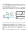
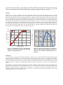
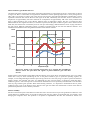
AQUARIUS: the next generation mid-IR detector for ground based
astronomy
Derek Ives*, Gert Finger, Gerd Jakob, Siegfried Eschbaumer, Leander Mehrgan, Manfred Meyer,
and Joerg Stegmeier
European Southern Observatory, Garching bei Munchen, Germany
ABSTRACT
ESO has recently funded the development of the AQUARIUS detector at Raytheon Vision Systems, a new mega-pixel
Si:As Impurity Band Conduction array for use in ground based astronomical applications at wavelengths between 3 – 28
µm. The array has been designed to have low noise, low dark current, switchable gain and be read out at very high frame
rates. It has 64 individual outputs capable of pixel read rates of 3MHz, implying continuous data-rates in excess of 300
Mbytes/second. It is scheduled for deployment into the VISIR instrument at the VLT in 2012, for next generation VLTI
instruments and base-lined for METIS, the mid-IR candidate instrument for the E-ELT. A new mid-IR test facility has
been developed for AQUARIUS detector development which includes a low thermal background cryostat, high speed
cryogenic pre-amplification and high speed data acquisition and detector operation at 5K. We report on all the major
performance aspects of this new detector including conversion gain, read noise, dark generation rate, linearity, well
capacity, pixel operability, low frequency noise, persistence and electrical cross-talk. We describe the many possible
readout modes of this detector and their application. We also report on external issues with the operation of these
detectors at such low temperatures. Finally we report on the electronic developments required to operate such a detector
at the required high data rates and in a typical mid-IR instrument.
Keywords: AQUARIUS, Si:As, Impurity Band Conduction Detector, Blocked Impurity Band Detector
1. INTRODUCTION
ESO has funded the development of a new Si:As Impurity Band Conduction (IBC) array, code-named AQUARIUS, at
Raytheon Vision Systems, Santa Barbara, USA. Si:As is an ideal material match to the astronomical wavelengths of
interest (3 – 28 µm) and has been in continuous product development and in astronomical use for at least two decades in
instruments such TIMMI2 at ESO and MICHELLE at GEMINI. Five science devices, an engineering grade and
multiplexers have been delivered to ESO, as part of this contract. An immediate need for the detector was to upgrade the
VISIR [1] instrument at the VLT. AQUARIUS has 1024 x 1024 pixels, each 30 µm2 in size and is therefore
approximately five to six times bigger in area than the previous generation of high background mid-IR detectors.
Chapter 2 gives a very brief introduction to the construction and detector physics of IBC detectors, followed by a more
detailed description of the pixel cell architecture, clock control and read modes available in the new AQUARIUS
detector. Chapter 3 describes the experimental setup used at ESO for initial testing and characterization of the new
detector. A typical mid-IR test facility should allow detector cooling to 5K and must have a very low thermal
background which typically means cooling the optics 40K. In this chapter particular emphasis is placed on the detector
thermal design and noise associated with the cycle time of the cryostat coolers as well as details of the complex
electronics required to operate the detector, optimally. Mid-IR detectors must be read out at very high frames rates,
implying very large real time data rates and video interface electronics which must operate at much higher pixel
frequencies than is typical for an IR detector. Chapter 4 gives a detailed overview of the laboratory results to date. This
includes a report on the usual detector characteristics which are most relevant to the use of such a device in a ground
based astronomical context. Finally, Chapter 5 concludes with a summary of the present status of our work and outlines
the areas where more testing is still required.
*[email protected]: phone: +49 89 32006921
2. DEVICE DESCRIPTION
Detector physics description
Impurity Band Conduction (IBC, Raytheon designation) or Blocked Impurity Band (BIB, Rockwell designation) photodetectors, were invented by Petroff and Stapelbroek [2] and are used for the astronomical mid-infrared range from 3 µm
to 40 µm wavelength, depending on the chosen impurity material of the detector. This wavelength range has
considerable importance in astronomy since the molecular and atomic emission lines from particular molecules are
within this range and far away objects are often hidden by interstellar dust clouds which absorb higher energy photons
and then re-admit mid-IR photons.
IBC detectors can deliver higher quantum efficiency in a volume much smaller than in conventional photo-conductors
because of their much higher primary doping. As a reference, an infra-red photo-conductor made of extrinsic silicon or
germanium would need to be very thick, of the order of 1mm or more in length through the detection volume, to absorb
most of the incident IR radiation. This makes the construction of good photo-conductors, very difficult. Photoconductors of this scale usually suffer from many other unwanted characteristics such as large electrical crosstalk,
transient response issues with memory like effects and sensitivity to high energy particles. To increase the sensitivity of a
photo-conductor and minimize its thickness means increasing the doping of the material. The more heavily doped the
material it is then the closer the doping impurities become on average. This increased impurity doping aids the hopping
conduction mechanism where the shallow impurities become the most important provider for free carriers as their
ionization energy is much lower than the intrinsic material’s band-gap. However this increased doping increases the
chances of trapped carriers to tunnel from one impurity to another without the need for photo-ionisation. This tunneling
current is unwanted dark current and is minimised in an IBC detector by the use of a special very lightly doped or undoped layer called the Blocking Layer. The use of this blocking layer means that the doping can be at least two orders of
magnitude greater than in a bulk photo-conductor without such a layer.
A simple schematic view of a typical n-type IBC detector is shown in Figure 1a. It consists of a heavily, but not
degenerately doped layer of width d, typically 10 µm thick, with donor concentration ND ,typically doped to 5 x 1017cm-3,
so that the dopants form an impurity band in which carrier hopping occurs. Next to the active layer is an area of intrinsic
Si of width b where hopping conduction is strongly suppressed, the blocking layer. This blocking layer which is very
lightly doped compared to the active layer has no impurities in which to hop and thus blocks the impurity band. Photoexcited carriers can still make it through the structure to the electrical contacts because the blocking layer and heavily
doped active area have the same valence and conduction bands. If the n-type detector, in the diagram shown, has a
voltage applied across it, such that the electrode on the blocking layer is positive with respect to the substrate side, then
an electron will move toward this electrode. Detectors can be front or back illuminated. Figure 1b shows the basic
architecture of a typical back illuminated IBC detector as given in the user manual for the AQUARIUS detector [3]. This
shows the typical structure of a pixel together with the indium bump contact which is used to connect to an external
multiplexer circuit.
IR radiation
Figure 1a: Typical structure for an n-type IBC detector Figure 1b: Basic architecture of a back illuminated IBC
detector, from AQUARIUS user manual.
AQUARIUS pixel cell architecture
In AQUARIUS the readout unit cell input circuit is the standard “3T” source follower per detector (SFD) direct
integration configuration plus the addition of two further FETs for enhanced functionality. The 3T unit cell circuit offers
several advantages over other designs: 1) only three transistors are required in the unit cell (source follower FET, address
FET, and reset FET), so smaller pixel sizes can be accommodated; 2) the SFD can be turned off during the signal
integration period so that there is virtually no power dissipation in the unit cell until the SFD is briefly turned on for
readout; and 3) the SFD can offer extremely low noise performance.
Of course the SFD has disadvantages: 1) the trans-impedance (output voltage divided by photons in) depends upon the
size of the detector junction capacitance, which is a non-linear function of detector bias; and 2) the input voltage swing
on the input node, which partly determines the dynamic range of the array, depends upon the reverse bias I-V
characteristics of the detectors and good detector diode reverse bias characteristics are required to insure good dynamic
range. Figure 2a is a schematic representation of the AQUARIUS unit cell [3]. It shows the three transistors as
described.
1
“3T” unit cell
0.9
y = 0.6061x
Measured output voltage (V)
0.8
0.7
0.6
0.5
0.4
0.3
0.2
0.1
0
0
0.5
1
1.5
VucRst (V)
Figure 2a: AQUARIUS detector unit cell design
Figure 2b: AQUARIUS Internal Transfer Function
As already stated, the AQUARIUS detector has two other FETs per unit cell to give increased functionalility and
performance. One FET, labelled MGAIN, allows a second capacitor to be switched into or out of each individual unit cell
to give a corresponding change in the capacitance of the unit cell. This additional capacitance has been designed in to
allow a factor of ten increase in unit cell full well capacity but with a corresponding decrease in the unit cell
transimpedance conversion gain and a corresponding increase in read noise. This allows the same unit cell to operate in a
high background regime such as in a mid-IR imaging camera where the sky is always very bright and at the same time
be used for high resolution, low background and low noise spectroscopy. The second extra FET MSH, allows user control
over a sample-and-hold capacitor, CSH. Typically, this FET switch is always active and on. However it can be switched
to give very short integration times, of the order of micro-seconds. This will allow operation of the detector in very high
background regimes such that the minimum integration time is no longer set by the frame read time of the array but is set
only by the array reset to switch off time of this FET and can be of the order of micro-seconds.
For AQUARIUS there are 1024 x 1024 of these unit cell pixels each of which is indium bump bonded to the individual
Si:As detector diodes, as seen in Figure 1b, using a standard hybridisation process which is typical for astronomical IR
detectors.
Figure 2b shows the internal transfer function for the detector when operated both at room temperature and cold,
indicating that little or no change is observed in this transfer function either warm or cold. For this plot, the voltage
across the IR diodes was set to zero volts by ensuring that the biases across the diodes set by VdetCom and VucRst are
equal. These voltages are then swung from 3.3V downwards to 1.5V, in small steps. The output voltage was then
measured and a plot of input to output voltage was plotted. The slope of this plot gives the internal transfer function or
gain from detector diode to output stage. For our detectors we typically measure a factor of 0.6 to 0.7, which seems low.
The reason for this is not yet fully understood at present.
In the bare multiplexer, which has not been hybridized to IR material, photo-generated electron-holes can still be
generated and these will usually be separated by a parasitic n-p junction in the unit cell, typically the reset FET. The
multiplexer is therefore responsive to optical light but it integrates in the opposite direction to the real IR diodes.
However the optical responsitivity of the mutiplexer is useful and has been used for early system level testing and warm
instrument optical alignment, since it offers a useful dynamic range of approximately twenty percent of the real detector.
Detector read out architecture and packaging
The architecture of the detector is such that it is split into two areas each of 512 rows and 1024 columns, at the top and
bottom of the device, as shown in Figure 3a. Each area has 32 outputs, such that, each output is configured to read out 32
x 512 pixels, all 64 outputs from the two areas being read in parallel. This readout scheme also allows for 16 outputs
rather than 64 to simplify system design for low background applications. With this multiplexer configuration it is
possible to read the detector out at 150 Hz frame rates, each output operational at 3 MHz pixel rates. A windowed
readout is also possible, where a user selectable number of rows can be read, from the center outwards, with the
remaining rows reset automatically. For example, a 1024 x 150 sized window, centred in the middle of the device, can be
readout at 1 kHz frame rates. There is no advantage to windowing in the column direction since all outputs run in
parallel.
All the typical detector read out modes are available and user-programmable with the simple control of five external
clock control lines. These readout modes include, Global Reset where all pixels are reset at the same time; Rolling mode,
where a row is read then immediately reset, then the next row is read and reset and so on, for a programmable row time
which can overlap the read of the next row; Non-Destructive Read without reset and Row Reset Level Read (RRLR)
where a row can be reset then read. Correlated Double Sampling, Fowler Sampling and Up-The-Ramp Sampling can all
be implemented using any combination of these different read out modes. The multiplexer also has test rows, top and
bottom and each output row of 32 pixels also has an on-chip generated reference level which can be read out and used
for low frequency noise surpression.
Figure 3a: AQUARIUS multiplexing readout scheme
Figure 3b: AQUARIUS MUX mounted in its socket
The detector is packaged into an Raytheon Aladdin III ceramic carrier as showns in Figure 3b, this package type was
chosen to reduce the overall manufacturing costs. It obviously does not allow for butting of detectors which would be
possible with a different package type. The ceramic carrier sits on a 124 pin LCC socket which is soldered onto a multilayer PCB. A cold finger projects through a large hole in the centre of the PCB and socket to the back of the detector to
cool it to the desired temperature. Indium foil should be used between detector package back surface and the cold finger
to ensure good thermal contact. Bespoke woven ribbon cables [4], specifically designed for use with AQUARIUS by us,
with twisted pairs, made from 40 SWG manganin wire and terminated with minature sockets at each end provide an
excellent thermal break but good electrical contact to the detector. These woven cables are clamped to the 40K stage at
the end away from the detector PCB. Detector dark current limited performance has been achieved with this
configuration and the minium operating temperature achieved for our detector was 5K. More woven copper ribbon
cables connect from the 40K cold stage to a cryogenic preamplifier which is typically operated at 100K. This amplifier
also has mounted on its PCB, the constant current loads required for operation of the outputs of the detector. The fully
differential output signals then connect from the preamplifier via more copper twisted pair woven cables to the hermetic
connectors and then to the data acquisition system.
3. EXPERIMENTAL SETUP
Cryostat and Electronics
All detector tests and characterisation were performed in TIMMI2 [5], an instrument which was originally used at ESO’s
La Silla Observatory but has now been decommissioned and redeployed at ESO’s headquarters. TIMMI2 was a full
common user astronomical instrument which included a full set of narrow and broadband filters, plate scale optics, slit
wheel and cold pupil design. It includes a Sumitomo CSW-71 two stage closed Cycle Cryo-cooler which has a 3K/1W
second cold stage. The instrument was heavily modified and upgraded to allow installation of the AQUARIUS detector
with the addition of a new cryogenic preamplifier and operation with ESO’s NGC [6], the new detector controller. This
new setup allows us to cool the fully operational detector to 5K and upwards. Typically, power dissipation of
AQUARIUS is dominated by the 64 outputs and has been measured, by indirect means, to be approximately 200-250
mW when operational and running at standard frame rates. At present, detector quantum efficiency measurements are
not directly measureable in TIMMI2 but must include the optical throughput of the instrument also. It was also found
that TIMMI2 has a large thermal background which made dark current measurements difficult to do; this meant
installing a cold blank directly in front of the detector to measure the dark current, results for which are reported later.
The ESO NGC system was used to drive the detector and digitize its outputs. The required configuration has 64 video
channels which operate in parallel and which have 16 bit, 3 MHz ADCs for each detector output. Typical date rates from
this system at standard detector frame rates are 300 Mbytes/second which in our burst mode, where all raw frames are
stored, can be sustained for many hours with the NGC detector electronics. A new PCIe interface board was also
developed to deal with these high data rates and this is fitted to a high specification server PC with multi-core CPUs,
extended memory and Terabytes of RAID hard disk storage. One issue for the NGC system was that it requires the input
video signals from the detector to be within the range of 0V to 5V for the ADCs, whereas the output of AQUARIUS is
typically 7V at starvation and 6V at saturation, swinging downwards. This meant that voltage level shifting of the
detector output video signal was required from 7V down to 0V, repeated 64 times and before the NGC input video
stages. This was implemented in new Level Shifting electronics which have been specifically designed for AQUARIUS.
Cryogenic preamplifiers, operational at 100K, were also designed and implemented. Our video circuit requirement was
for a fully differential amplifier circuit with a gain of three which would operate at 100K and have the bandwidth, slew
rate and low noise characteristics (6nv/√Hz) needed to match the detector performance. CMOS op-amps are required to
meet these specifications but the only devices available, the OPA354 from Texas Instruments, must be operated with a
maximum 6V supply. We therefore chose to operate our design with a +10V current source/+4V current sink
configuration to match the detector outputs. Constant current loads are also connected to each of the 64 detector outputs.
These current sources were originally developed for the ORION 2Kx2K InSb array from Raytheon. They consist of two
integrated chips, operating at temperatures greater than 25K, each with 32 current sources which have been packaged by
us specifically to be used for the AQUARIUS video outputs. The current is user controllable from a single NGC bias
voltage, controllable between 300-600 µA, which is the great advantage of using this type of load. They also minimize
the effect of cable resistance on the overall detector linearity; this resistance can be relatively large for a mid-IR
configuration because cables with low thermal conductivity but high resistance such as manganin are used.
Thermal Oscillations
Typically the closed cycle coolers used in astronomical instruments for cooling the detectors and optics do not provide a
constant temperature in their cooling cycle. There is usually a thermal oscillation of the cold head which has a frequency
of 1 Hz, the typical operating frequency of the cold head solenoid, with a peak-to-peak amplitude of approximately a few
tenths of a Kelvin. These thermal oscillations can result in additional detector noise because the detector output voltage is
sensitive to this temperature change; this is clearly seen in Figure 4a which is a plot of detector signal level against time
for a constant illumination. The change of output is seen to be 250 DN which in our system would equate to an additional
noise of approximately 50 e- rms added in quadrature to the read noise.
Figure 4b shows our solution to this problem in which we have mounted a large block of lead, approximately 0.6kg in
weight, between the cryo-cooler’s copper cold finger and the detector cold finger. Lead has a higher specific heat (10
J/kg.K) than copper (0.85 J/kg.K) at 10K and is therefore less responsive to temperature changes, this has the effect of
smoothing the thermal oscillation by a factor of at least fifty for our design.
3K cold finger
Lead block
Manganin weave cables
Figure 4a: Thermal oscillation seen on detector
output as a plot of signal for constant flux against
time
Figure 4b: Detector mount showing addition of
lead to minimise thermal oscillation
4. PRESENTATION OF RESULTS
At the present time two science grade devices and one engineering device have been tested in our laboratory. The
devices were graded by Raytheon as meeting the science specifications, principally in terms of their cosmetic quality.
The results given here were taken under a set of nominal operating conditions found to give good performance rather
than the absolute best performance in any one category. Figure 5a is a table giving the specifications for the detector
together with a summary of the actual characteristics which have been measured.
Specification
Goal
Measured
Array size (pixels)
1024 x 1024
1024 x 1024
Pixel Size (microns)
30 , ~ 100% fill factor
30
Operating Temperature
6-9K
8K to be used at telescope
Frame Frequency and Data
Rate
120 Hz => 300 Mbytes/seconds
120Hz typical but 150Hz shown but not
yet characterized
Quantum Efficiency at 10 µm
>50% with anti-reflection coating
To be measured
Spectral Response
5 to 28 µm(Si:As detector material)
To be measured
Integration capacity
1x10⁶/10x106 electrons
0.6x10⁶/5x106 electrons
Input referred noise
100e/1000e rms
150/1400 e rms for single read, fixed
pattern noise corrected
Non-Linearity
<5%
< 2% for ¼ to ¾ full well
Power Dissipation
< 150 mW
~ 200mW measured for 64 outputs with
500 uA current loads
Dark Current
1 e/pixel/second at 7K
Achieved ~ 1.3e/pixel/second at 7K
Crosstalk
< 1% to adjacent pixels
~6-7% to adjacent pixels
Figure 5: Summary of device performance measurements
Dark Current
A big challenge for mid-IR detectors is to minimise the leakage and dark current but still ensure that the device operates
at temperatures within the operating range of Closed Cycle Coolers. Typically the required operating temperature is
somewhere between 6-9K. An Arrhenius plot for one of our science grade devices is shown in Figure 6a. A table is given
in Figure 6b to give the reader a more precise indication of the dark current measurements.
The dark current is shown to be approximately 1 electron/pixel/second at an operating temperature of 7K which is an
excellent result. Lower dark currents are possible but no effort has gone in to making exact measurements at these lower
temperatures because the dark current easily meets our operational goal.
loge(dark current) - electrons/pixel/second
10
9
Temperature (K)
8
Bias=1.9V
7
y = -210.84x + 28.826
6
5
4
Bias=1.3V
3
2
1
Dark Current (e/pix/s)
6.5
0.56
7.0
1.30
7.5
2.70
8.0
12.6
8.5
56.6
9.0
210.8
9.5
715.2
10.0
2199.8
0
0.08
0.1
0.12
1/Temperature (K)
0.14
0.16
Figure 6a: Typical Arrhenius plot of dark current for
two different reverse bias voltages, showing
exponential dependence of thermal activation.
Figure 6b: Table of dark current versus temperature.
If we assume that the dark current is of the form given in the following equation, where Id is the dark current, Io is a
constant, Egap is the band gap energy, x is some factor dependent on the dark current processes, k is Boltzmann’s constant
and T is the detector temperature. Then making some simple assumptions and inserting the expected activation energy
for Si:As, at 28 µm and the slope into the equation gives a value for x of approximately two. This implies that the dark
current is as expected for a photo-conductive material and is typically generation-recombination limited.
Linearity
Figure 7a gives a plot of exposure time against measured signal level for both the high gain and the low gain
configurations. Typically this data is taken in a non-destructive read mode such that many hundreds of frames are taken
from the signal starvation level to the signal saturation level. Between 15k DN and 40k DN a linear fit is made to each
data set. The difference between the measured data and the line fit data is then calculated as a percentage of the line fit
data to determine the non-linearity of the detector. This difference as a percentage of signal level is shown in Figure 7b
for high gain and indicates that this particular detector’s linearity is good to +/-0.5% over the specified signal range
given. The fitted trend-lines are also displayed on the plots in Figure 7a, together with the equations for these trend-lines.
The difference in the gradients of each of these two trend-lines gives an exact measure of the gain change between the
low gain and the high gain configurations. For this particular detector, the gain and therefore the detector saturation level
and read noise can be changed by a factor of approximately eight.
60000
0.5
Low Gain
0.3
y = 328814x - 5763.1
0.2
40000
% Non-Linearity
Signal Level (DN)
0.4
High Gain
50000
0.1
30000
y = 40815x - 4146.8
0
-0.1
20000
0
10000
20000
30000
40000
50000
Signal Level (DN)
-0.2
-0.3
10000
-0.4
0
0
0.5
1
1.5
Exposure time (s)
2
2.5
Figure 7a: Typical linear plot for both high and
low gain read modes. The slope gives the gain
change to be approximately x 8.
-0.5
Figure 7b: Detector non-linearity as a function of
signal level for high gain. Computed by fixing a
slope to the data and measuring the difference to
the slope.
Read Noise
The read noise for a single read in the high gain mode is typically 150 e- rms and assumed to be approximately the gain
factor of eight higher than this for the low gain mode. The read noise is also seen to be a function of temperature,
excluding any dark current shot noise, as shown Figure 8a and assuming that the detector trans-impedance conversion
gain is the same for both warm and cold operation. This plot indicates that the read noise is approximately 60µV at room
temperature but at a temperature of approximately 25K the read noise increases by a factor of six, to approximately
350µV.
This behaviour of the read noise has been seen in the past in detectors which must be operated at extremely low
temperatures, for example, in the InSb Aladdin III device; the issue has also been reported [7] in the development of the
Raytheon SB-226 multiplexer for MIRI detector on JWST. It is understood that many of the foundries and silicon
multiplexer designers have noise models which are accurate to 77K but these models then breakdown for the colder
operating temperatures of these detector types.
At room temperature the kTC noise can be seen in the detector and from design and modelling analysis, should be the
dominant noise source, implying the use of Correlated Double Sampling (CDS) to remove this noise source. The kTC
noise is most easily seen by comparing the noise in a CDS frame compared to the noise in the difference between two
SIMPLE-RESET-READ (SRR) frames, which will have twice the kTC noise in them which would then add in
quadrature.
350
400
300
350
300
250
Read Noise (e- rms)
Read Noise (uV)
250
200
200
150
150
100
100
50
50
0
0
0
20
40
60
Temperature (K)
80
Figure 8a: Read noise versus detector operating
temperature.
1
10
100
1000
Number of non-destructive reads
Figure 8b: Read noise versus number of nondestructive reads
From this analysis and testing it can be shown that the kTC noise is approximately 60µV, at room temperature, which is
in reasonable agreement with the calculated kTC noise of the unit cell capacitance. However since the read noise
increases so dramatically when cooling the detector to below 25K, then the dominant noise source becomes the output
source follower read noise and the kTC noise becomes negligible. Again this can be checked using the method already
described which gives the result that the CDS noise equals the noise for the difference of two SRR frames when
operating the detector cold, because there is low kTC noise. This is a very important result as it means that the Correlated
Double Sampling method does not need to be used when reading the detector out. A simple RESET and then READ of
the detector is the optimal read mode. However the main issue when not subtracting frames as per the CDS algorithm is
that the fixed pattern noise would then be the dominant noise source. Typical for a mid-IR instrument, the detector will
always be used at the telescope with chopping and nodding sequences of the secondary mirror to subtract out the very
bright sky component. The net result of this is that the fixed pattern noise is automatically subtracted out as a
consequence of these chop and nod cycles.
Multiple sampling techniques substantially reduce the readout noise as can be seen in Figure 8b which shows the readout
noise versus the number of non-destructive readouts. The readout time for a single non-destructive readout is 8.5 ms.
The detector is continuously read out in the non-destructive mode and processed using the Fowler algorithm. The
detector integration time for 512 non-destructive reads is then less than 5 seconds. The lowest readout noise measured is
approximately 24 e- rms for the 512 reads, fixed pattern subtracted. Data taking was stopped at this point but the plot
seems to indicate that the noise is still on a downward trend and even lower noise should be possible. This is an
outstanding result for a mid-IR detector and shows that the AQUARIUS detector could even be used for low flux
applications in space or for extremely high resolution ground based experiments in L and M band where the photon
background level is below 0.1 electron/pixel/second.
Pixel nearest neighbour correlation
The detectors were tested for capacitive coupling and other types of correlation between a particular pixel and its nearest
neighbour pixels. This test was performed by taking many hundreds of flat field images which are photon shot noise
dominated and then using the differences of the consecutive images to measure the pixel auto-correlation. The results of
this test are shown in Figure 9a as a two dimensional image. Figure 9b re-interprets these results as a plot along the
column and row of the central pixel of the image. This gives a measure of the coupling to the nearest neighbour pixels
and is typically 6-7% for the four cardinal pixels. The image also shows that there is a correlation with any pixel which is
positioned 32 pixels away along the same row, on both sides. This indicates that the same pixel of the same row for
every output has a low level correlation, of the order of 1%, to the same pixel in every other output. This would typically
manifest itself as a “ghost” image being observed in an image frame at every other output position for a bright object in
one particular output.
Figure 9a: 2D autocorrelation result for flat field.
Image shows the correlation of any pixel to its
nearest neighbouring pixels. Highlighted are
pixels 32 columns away on same row.
Figure 9b: 2D autocorrelation result for rows
(top) and columns (bottom).
In fact these ghosts are most clearly seen in Figure 10a, which is the difference of two image frames, in which a spot has
been projected onto the detector and then moved slightly between the two frames.
Real spots
Ghost spots
Figure 10a: Difference image for spot projected onto
detector and then moved slightly for second image.
Image highlights the “Ghosting” to all other outputs.
Figure 10b: Column block averaged image to
emphasis the odd-even column effect of the
detector, of the order of ~ 1-2% of signal level.
The coupling into all other 63 outputs is then easily seen as two ghost images, which are repeated for every spot on every
output. If the spots are projected onto the top of the detector then the coupling is the same for both top and bottom
outputs and vice-versa. This coupling is obviously to do with the impedance of the power and ground rails to the detector
outputs which are most likely shared.
The auto-correlation data also hints at a column-wise correlation between pixels and its neighbours along the same
column. Flat field data was averaged in the column direction to highlight this column effect. The result is most clearly
seen in Figure 10b which is a flat field image of a small detector region which has been averaged in the column direction,
showing the column effect, the level of which is typically of the order of approximately 1-2% of the signal level.
Excess Noise in Low Gain Mode
Figures 11a and 11b show standard photon transfer curves, where noise versus signal is plotted on a log-log scale, for
both the high gain and low gain configurations, respectively. The plots also give theoretical plots for a detector with
similar gain and read noise and also zero read noise. The detector, when operated in high gain mode, performs well, with
the plot indicating that the detector will be photon shot noise limited. However the plot for the low gain configuration
indicates that there is an excess noise issue which is signal dependent. This is shown in the plot by the red arrow. At
present it is not understood the source of this noise. The difference between the two modes in the unit cell is the FET
switch MGAIN used to switch the extra capacitance into or out of the unit cell. Possibly the FET Drain-Source channel
resistance is not linear or as low as expected with integrated voltage at the low operating temperature. Tests have been
performed to try to turn the switch on harder but this seems to have little effect. Another possibility is that there is photoconductive gain and associated gain dispersion adding in noise, but this seems unlikely to cause this excess noise; see the
next section for further detail. Further tests are required to determine the exact source of this excess noise. The noise
seems to be of the order of twice the photon shot noise. The presence of this excess noise means that for single reads in
the low gain mode and high signal regime, then the detector will never be photon shot noise limited. This data was taken
in both the spatial domain where the noise is calculated for small windows placed in different parts of the detector and
also temporally where the noise on a single pixel is calculated and then averaged for many pixels. The results were the
same for both cases.
Excess Noise
Figure 11a: Photon Transfer Curve for AQUARIUS
detector in HIGH gain configuration. The dashed lines
are for simulated data with and without read noise.
Figure 11b: Photon Transfer Curve for AQUARIUS
detector in LOW gain configuration.
Photo-conductive gain in IBC detectors
One final result worth reporting is the effect of operating temperature on output signal level for a constant flux as shown
in Figure 12a. Here a constant flux is integrated onto the detector and the operating temperature is slowly changed from
5K to 12K. Two regions are clearly seen in the plot. First the region to the right and indicated by a dashed line is easily
explained as detector dark current. However the region to the left, indicated by the solid line, shows a maximum at a
temperature of approximately 7K and a minimum at a temperature of approximately 10K. This clearly indicates that
there is photo-conductive gain in the detector material which is temperature related. The plot is repeated for three
different detector bias regimes and shows, as would be expected, that the photo-conductive gain is also a function of the
diode bias, the bias has been increased by 0.3V for each plot. Interestingly, different detectors show varying amounts of
this gain and at different temperatures which is probably associated with the fact that the different detectors were
manufactured at different times using different batches of the detector material.
25000
Photo-conductive gain
20000
Increasing detector bias
Signal (DN)
Dark Current
15000
10000
5000
0
0
2
4
6
8
Temperature (K)
10
12
14
Figure 12a: Signal versus operating temperature for a constant flux and different
detector biases. The plot shows the regions of photo-conductive gain and dark
current.
Simple analysis of the Signal-to-Noise Ratio indicates that the excess noise factor associated with the gain is low which
means that it may be worth considering the use of the photo-conductive gain in particular operating regimes, for
example, in low background high resolution spectroscopy. However at this early stage we plan to operate the detectors
slightly warmer with minimal gain until we understand the gain processes better. It should be noted that photoconductive gain is a well known process in this material and detectors can be specifically manufactured to use this effect
with very large internal gains possible. When characterizing a detector, it is important to understand if there is photoconductive gain or not in the detector setup, otherwise this gain will affect the measurement of most of the detector
performance parameters such as linearity and noise.
Detector Stability
We have tested some aspects of the detector which have been a serious concern in previous generations of detectors. The
present detector in VISIR requires 10 seconds of settling time after any change of operational state, for example, when
changing the integration time. This problem is not present in AQUARIUS. We have also checked for Excess Low
Frequency Noise (EFLN) [8] which was an issue in the past in this detector type; some EFLN is seen but of the order of
approximately 10%. Further reporting will be made on these aspects in a future publication.
5. CONCLUSIONS
Two new AQUARIUS detectors, their development funded by ESO and designed and manufactured at Raytheon have
now been tested and are ready for installation into our mid-IR instrument VISIR at the VLT. We have measured many of
the typical performance parameters such as dark current, read noise, linearity and stability and believe that the
AQUARIUS detector sets a new standard for ground based mid-IR detectors. With the proposed detector and optical
changes to VISIR we hope to increase our observing efficiency by an order of magnitude. The detector is capable of
maintaining very high performance in both the low and high flux regimes. Non-destructive read modes give excellent
low noise performance and may be implemented for the first time on the VISIR instrument. There are still some issues
which need to be understood and possibly addressed in future design updates such as the excess noise in the low gain
configuration and the coupling to nearest neighbour pixels. More detailed testing is still required, for example, we are not
yet setup to do quantum efficiency tests of the detector or are able to determine the cut-off wavelength. We typically
operate the detector at 120 Hz frame rates but know that much faster rates are possible but need still need
characterization.
6. ACKNOWLEDGEMENTS
We are particularly indebted to the design and test staff, past and present, at Raytheon, with a particular mention for Eric
Beuville, the lead design engineer for AQUARIUS and to external consultant Alan Hoffman, for his knowledge and
support of IBC detector technology. This project would not have been possible without them. The development of the
NGC detector control system at ESO has allowed us to operate the detector at its maximum potential and has been made
possible by the highly skilled electronics and software engineers in the Detector Group at ESO. A final mention should
be made of the ESO Cryogenics Dept. who made TIMMI2 such an excellent mid-IR test facility.
7. REFERENCE
1.
Lagage P.O. et al., "VISIR VLT Imager and Spectrometer for mid-IR," The ESO Messenger 117, 12 (2004).
2.
Michael Petroff and Maryn Stapelbroek," US Patent Number 4,568,960, Blocked Impurity Band Detectors,"
(1986)
3.
Eric Beuville, "SB383 Aquarius, 1k x 1k User's Guide, Version 1.3," (2009)
4.
http://www.cryoconnect.com/home/
5.
Kaeufl Hans-Ulrich, Sterzik Michael F., Siebenmorgen Ralf, Relke Helena, Stecklum Bringfried, "Polarimetric
mode of TIMM12: technical characteristics and first results," Proc. SPIE, 4843 233-240 (2003).
6.
http://www.eso.org/projects/ngc/
7.
Ken Ando, Alan Hoffman, Peter Love, Andrew Toth, Conrad Anderson, George Chapman, Craig McCreight,
Kimberly Ennico, Mark McKelvey, Robert McMurray Jr., "Development of Si:As Impurity Band Conduction
(IBC) Detectors for Mid-Infrared Applications," Proc SPIE, 5074 (2003) .
8.
Stapelbroek M. G., Seib D. H., Huffman J.E., Florence R. A., "Large-format Blocked-Impurity-Band focal
plane arrays for long-wavelength infrared astronomy," Pro. SPIE, 2475, 41-48, (1995)