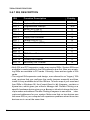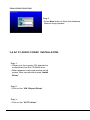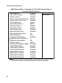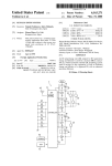
1
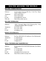
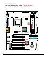
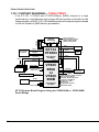
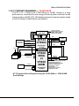
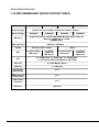
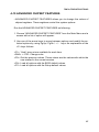
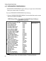
R
SL-75KV+/75KV2/75JV/75JV2
USER MANUAL V1.1
USER NOTICE
Product Model
Manual Revision
Release Date
: SL-75KV+/KV2/JV/JV2
: V1.1
: September 2000
his Users Guide & Technical Reference is for assisting system
manufacturers and end-users in setting up and installing the
mainboard.
Every effort has been made to ensure that the information in this
manual is accurate. Soltek Computer Inc. is not responsible for printing or clerical errors. Information in this document is subject to
change without notice and does not represent a commitment on the
part of Soltek Computer Inc.
No part of this manual may be reproduced, transmitted, translated
into any language in any form or by any means, electronic or
mechanical, including photocopying and recording, for any purpose
without the express written permission of Soltek Computer Inc.
Companies and products mentioned in this manual are for identification purpose only. Product names appearing in this manual may
or may not be registered trademarks or copyrights of their respective companies.
T
Soltek computer inc. Provides this manual “As is “ without warranty of any kind, either express or implied, including but not limited
to the implied warranties or conditions of merchantability or fitness
for a particular purpose. In no event shall Soltek computer inc. Be
liable for any loss or profits, loss of business, loss of use or data,
interruption of business, or for indirect, special, incidental, or consequential damages of any kind, even if Soltek computer inc. Has
been advised of the possibility of such damages arising from any
defect or error in this manual or product.
Copyright © 2000 Soltek Computer Inc. All Rights Reserved.
• AMD Athlon ThunderbirdTM, and DuronTM processors are trademarks of AMD Corporation.
• VIA, KT-133, VT8363 and VT82C686A are trademarks of VIA Corporation.
• Norton AntiVirus, Norton Ghost are trademarks of Symantec Corporation.
SOLTEK AROUND THE WORLD
SOLTEK COMPUTER INC.
Address
Telephone
Fax
E-mail
Web site
: 7F, No. 306-3, Ta-Tung Rd, Sec.1, Hsi-Chin, TaipeiHsien, Taiwan, R.O.C.
: 886-2-2642-9060
: 886-2-2642-9065
: [email protected]
: http://www.soltek.com.tw
SOLTEK KOREA INC.
Address
Telephone
Fax
E-mail
: 1002, Chungjin Bldg. 53-5 Wonhyo-Ro, 3-Ka,
Yongsan-Ku Seoul 140-113, Korea
: 82-2-32717400
: 82-2-32717405
: [email protected]
MOKA HOLDING B.V.
Address
Telephone
Fax
E-mail
: De Run 4428 5503 LR Veldhoven, the Netherlands
: 31-402-556150
: 31-402-546006
: [email protected]
SOUL TECHNOLOGY EUROPE B.V.
Address
Telephone
Fax
E-mail
Web site
: Sydneystraat 52-54 3047 BP Rotterdam, the Netherlands
: 31-10-2457492
: 31-10-2457493
: [email protected]
: http://www.soultech-europe.com
75KV+/75KV2/75JV/75JV2
CONTENT
Chapter 1
INTRODUCTION .......................................................... 7
1-1 ITEM LIST CHECKUP .................................................................. 7
1-2 PROCESSOR ............................................................................... 7
1-3 CHIPSET ...................................................................................... 7
1-4 ADVANCED HIGH PERFORMANCE DRAM CONTROLLER ...... 7
1-5 FULL FEATURED ACCELERATED GRAPHICS PORTS (AGP)
CONTROLLER .............................................................................. 8
1-6 MULTI-I/O FUNCTION .................................................................. 8
1-7 EXTENSION SLOTS .................................................................... 8
1-8 BIOS ............................................................................................. 9
1-9 SOUND CONTROLLER (FOR 75KV+ & 75KV2 ONLY) ............... 9
1-10 POWER MANAGEMENT ............................................................ 9
1-11 FROM FACTOR .......................................................................... 9
1-12 HARDWARE MONITORING ....................................................... 9
1-13 OTHERS ..................................................................................... 9
1-14.1 MOTHERBOARD LAYOUT --- 75KV+/75KV2 ....................... 10
1-14.2 MOTHERBOARD LAYOUT --- 75JV/75JV2 ........................... 11
1-15.1 CHIPSET DIAGRAM--- 75KV+/75KV2 .................................. 12
1-15.2 CHIPSET DIAGRAM --- 75JV/75JV2 ..................................... 13
1-16 MOTHERBOARD SPECIFICATION TABLE ............................. 14
Chapter 2
HARDWARE SETUP .................................................. 15
2-1 CPU INSTALLATION ..................................................................
2-2 AMD SOCKET A (SOCKET 462) PROCESSOR ........................
2-3 MEMORY INSTALLATION ..........................................................
2-4 ACCELERATED GRAPHICS PORT(AGP) PRO INSTALLATION ....
2-5 HDD / FDD INSTALLATION ........................................................
4
15
16
17
18
19
75KV+/75KV2/75JV/75JV2
2-6 CPU FREQUENCY ..................................................................... 20
2-7 BUS RATIO SELECT .................................................................. 21
2-8 JUMPER DEFINITIONS ............................................................. 23
2-8.1 ONBOARD FAN CONNECTOR (FAN1/FAN2) ........................ 23
2-8.2 USB PORT SELECT (JP1/JP2) ............................................... 24
2-8.3 FACTORY (JP3) ....................................................................... 24
2-8.4 POWER LOST RESUME (JP7) ............................................... 24
2-8.5 USB WAKE UP (JP9) .............................................................. 24
2-8.6 MEMORY MODULE VOLTAGE SELECT (JP10/JP11) ............ 25
2-8.7 CLEAR CMOS DATA (JBAT1) ................................................ 25
2-8.8 WAKE ON LAN FUNCTION (WOL1) ....................................... 26
2-8.9 CD-ROM AUDIO CONNECTOR (CD-IN1/CD-IN2) ................. 26
2-8.10 THERMAL SENSOR CONNECTOR (RT2) ........................... 26
2-9 CONNECTORS .......................................................................... 28
2-9.1 J3 AND J4 ............................................................................... 28
2-9.2 CHASSIS PANEL CONNECTOR ............................................ 31
2-9.3 ATX POWER SUPPLY CONNECTOR .................................... 32
2-9.4 SERIAL PORT CONNECTORS .............................................. 33
2-9.5 SECOND USB CONNECTOR ................................................ 34
2-9.6 PS/2 MOUSE AND PS/2 KEYBOARD .................................... 35
2-9.7 IRQ DESCRIPTION ................................................................. 36
2-9.8 VOICE DIAGNOSTIC FUNCTION----ONLY FOR 75KV+-X/KV2X/JV-X/JV2-X .......................................................................... 37
Chapter 3
SOFTWARE SETUP ................................................... 39
3-1 ABOUT SUPPORT CD ...............................................................
3-2 VIA CHIPSET DRIVER INSTALLATION (4-IN-1 DRIVER) .........
3-3 HARDWARE MONITOR INSTALLATION ...................................
3-4 AC 97 AUDIO CODEC INSTALLATION .....................................
39
39
43
44
5
75KV+/75KV2/75JV/75JV2
Chapter 4
BIOS Setup ................................................................ 46
4-1 INTRODUCE THE BIOS .............................................................
4-2 WHAT IS BIOS SETUP ...............................................................
4-3 HOW TO RUN BIOS SETUP ......................................................
4-4 WHAT IS CMOS .........................................................................
4-5 WHAT IS POST ..........................................................................
4-6 BIOS UPGRADE .........................................................................
4-6.1 BEFORE UPGRADE BIOS ......................................................
4-6.2 UPGRADE PROCESS .............................................................
4-7 CMOS SETUP UTILITY ..............................................................
4-8 STANDARD CMOS SETUP ........................................................
4-9 ADVANCED BIOS FEATURES ...................................................
4-10 ADVANCED CHIPSET FEATURES ..........................................
4-11 INTEGRATED PERIPHERALS .................................................
4-12 POWER MANAGEMENT SETUP .............................................
4-13 PNP / PCI CONFIGURATION ...................................................
4-14 PC HEALTH STATUS ...............................................................
4-15 FREQUENCY/VOLTAGE CONTROL .......................................
4-16 LOAD FAIL-SAFE DEFAULTS ..................................................
4-17 LOAD OPTIMIZED DEFAULTS ................................................
4-18 SET SUPERVISOR / USER PASSWORD ................................
4-19 SAVE & EXIT SETUP ...............................................................
4-20 EXIT WITHOUT SAVING ..........................................................
6
46
46
46
46
47
47
47
47
50
51
53
57
62
67
73
76
77
78
78
79
80
80
75KV+/75KV2/75JV/75JV2
CHAPTER 1
INTRODUCTION
1-1 ITEM LIST CHECKUP
• Motherboard
• Support CD
• User’s Manual
• Bundle Bonus Pack CD
• Bundle Bonus Pack Manual
• Temperature Sensor Cable
• ATA 66/100 IDE Cable
• Temperature Sensor Cable
• RS232 Cable
• FDD Cable
1-2 PROCESSOR
• Supports AMD Athlon Thunderbird processors up to 1.0GHz or higher
• Supports AMD Athlon Duron processors up to 750MHz or higher
• 200MHz AMD Athlon system bus.
• Supports processor VID (voltage ID) and FID (frequency ID) auto detection
1-3 CHIPSET
• North Bridge VIA VT8363 (KT-133) system controller High Performance
Athlon CPU Interface
• South bridge VIA VT82C686A or VIA VT82C686B
1-4 ADVANCED HIGH PERFORMANCE DRAM
CONTROLLER
• Supports PC133 and PC100 SDRAM and Virtual Channel Memory (VCM)
SDRAM up to 3 DIMMs
• 64-bit data width and 3.3V DRAM interface
• Supports up to 1.5 GB memory space
• Different DRAM types may be used in mixed combinations
• PCI-2.2 compliant, 32 bit 3.3V PCI interface with 5V tolerant inputs
7
75KV+/75KV2/75JV/75JV2
1-5 FULL FEATURED ACCELERATED GRAPHICS PORTS
(AGP) CONTROLLER
• Synchronous and pseudo-synchronous with the host CPU bus with optimal
skew control PCI AGP Mode 33MHz/66MHz/100MHz DDR 3x synchronous
• Supports 66MHz 1x, 2x and 4x modes for AD and SBA signaling
• AGP v2.0 compliant
1-6 MULTI-I/O FUNCTION
• Two UltraDMA 33/66 Master Mode PCI EIDE ports (for 75KV+ and 75JV
only)
• Two UltraDMA 33/66/100 Master Mode PCI EIDE ports (for 75KV2 and
75JV2 only)
• Two UARTs for complete Serial Ports
• One dedicated IR connector:
--Third serial port dedicated to IR function either through the two complete serial
ports or the third delicated port Infrared-IrDA (HPSIR) and ASK( Amplitude Shift
Keyed) IR
• Multi-mode parallel connector:
--Standard mode, ECP and EPP support
• Floppy Disk connector:
--Two FDDs with drive swap support
• Universal Serial Bus connector:
--USB v1.1 and Intel Universal HCI v1.1 compatible
--Provides 2 build-in USB ports (another 2 internal USB ports for extensible purpose
require an optional USB connect cable)
• PS/2 keyboard connector
• PS/2 Mouse connector
1-7 EXTENSION SLOTS
• Five PCI bus Master slots
• One ISA slot
• One AGP Pro 4x mode slot
• Three DIMM slots
8
75KV+/75KV2/75JV/75JV2
1-8 BIOS
• Award BIOS V6.0
• Supports Plug & Play V1.0
• Flash Memory for easy upgrade
• Year 2000 compliant
• Supports BIOS writing protection
1-9 SOUND CONTROLLER (FOR 75KV+ & 75KV2 ONLY)
• SoundBlaster Pro Hardware and Direct Sound Ready AC97 Digital Audio
Controller with Codec onboard
1-10 POWER MANAGEMENT
• ACPI 1.0 compliant (Advanced Configuration and Power Interface)
• APM V1.2 compliant (legacy power management)
• Supports ACPI suspend STR mode (Suspend To DRAM) and POS mode
(Power On Suspend)
• Supports Wake On LAN (WOL) & Wale On Modem
• Supports real time clock (RTC) with date alarm, month alarm, and century
field
• Supports USB boot-up Function
1-11 FROM FACTOR
• ATX from factor, 4 layers PCB
• Motherboard size 22.0cm x 30.5cm
1-12 HARDWARE MONITORING
• Programmable control, status, monitor and alarm for flexible desktop management (software include)
• Five-positive voltage monitoring
• Two-temperature monitoring
• 2 Fan-speed monitoring
1-13 OTHERS
• Clock generator supports 1 MHz linear clock setting
• Supports DRAM Voltage select Function
9
75KV+/75KV2/75JV/75JV2
1-14.1 MOTHERBOARD LAYOUT --- 75KV+/75KV2
• Default Setting: AMD Athlon ThunderbirdTM 100MHz.
5 4 3 2 1
DIP
ATX POWER
1
4 3 2 1
ON
DIP
SW1
1
1
SOCKET A
PC100/PC133 SDRAM
GAME/MIDI PORT
3
3
JP11
Clock
Generator
DIMM1
DIMM2
DIMM3
COM 1
LPT1
LINE
OUT
LINE
IN
SSF1
JP10
3
JP9
MIC
ON
SW2
FDD1
upper
upper
PS/2
USB0
MOUSE
lower
lower
PS/2
USB1
K/B
FAN1
VIA
KT-133
COM 2
4x AGP PRO
JP3
ZD1
IDE1
3 CD_IN2
3 CD_IN1
1
1
PCI 1
AC'97
Codec
IDE2
1
3
15
PWR/LED
+
-
ISA
RST
IR
FAN2
SPK
Li
Battery
PCI 5
W5280
10
T/LED
1
15
J3
J4
RT2
JBAT1
SMI
PCI 4
VIA
686A
or
686B
PWR
PCI 3
HDD/LED
3 JP1
3 JP2
+ - - +
1
1
15
1
WOL1
16
1
USB1
1
FLASH BIOS
2
JP7
3
PCI 2
75KV+/75KV2/75JV/75JV2
1-14.2 MOTHERBOARD LAYOUT --- 75JV/75JV2
• Default Setting: AMD Athlon ThunderbirdTM 100MHz.
5 4 3 2 1
DIP
ATX POWER
1
4 3 2 1
ON
DIP
SW1
SSF1
JP10
3
1
1
JP9
SOCKET A
3
3
JP11
PC100/PC133 SDRAM
Clock
Generator
DIMM1
DIMM2
DIMM3
COM 1
LPT1
ON
SW2
FDD1
upper
upper
PS/2
USB0
MOUSE
lower
lower
PS/2
USB1
K/B
FAN1
VIA
KT-133
COM 2
JP3
4x AGP PRO
ZD1
IDE1
PCI 1
IDE2
1
SMI
T/LED
PWR
3
15
JBAT1
1
15
J3
J4
RT2
ISA
W5280
IR
RST
SPK
Li
Battery
PCI 5
+
-
PCI 4
VIA
686A
or
686B
PWR/LED
PCI 3
HDD/LED
3 JP1
3 JP2
+ - - +
WOL1
1
1
15
1
1
16
1
USB1
FLASH BIOS
2
JP7
3
PCI 2
FAN2
11
75KV+/75KV2/75JV/75JV2
1-15.1 CHIPSET DIAGRAM--- 75KV+/75KV2
CFWDRST
PROCRDY
CONNECT
• The KT-133 / VT8363 and VT82C686A(or 686B) chipset is a high
performance, cost-effective and energy efficient system controller for the
implementation of AGP / PCI / ISA desktop personal computer system based
on 64-bit Socket-A (AMD Athlon) processors.
GCLK
3D Graphics
Controller
AGP Bus
GCKRUN#
PCKRUN#
PCLK
PCI Bus
BIOS ROM
ATA 33/66 or ATA 33/66/100
USB Ports 0 - 3
AC97 Audio Codec
AC97 Link
ISA Bus
RTC Crystal
Athlon
Host CPU
Address
Out
SYSCLK, SYSCLK#
INTR, NMI, SMI#, STPCLK#,
IGNNE#, FERR#, A20M#,
PWROK, INIT#, RESET#
Data
In
CKE
Memory Bus
KT133
VT8363
North Bridge
552 BGA
MCLK
SDRAM
Clock
Buffer
HCLK
PCLK
SUSCLK,
SUSST1#
VT82C
686A
or
VT82C
686B
South Bridge
352 BGA
CPUSTP#
PCISTP#
Clock
Generator
SMBus
Power Plane & Peripheral Control
GPIO and ACPI Events
Hardware Monitoring Inputs
Keyboard / PS2 Mouse
Serial Ports 1 and 2
Parallel Port
Floppy Drive Interface
MIDI / Game Ports
KT133 System Block Diagram Using the VT82C686A or VT82C686B
South Bridge
12
75KV+/75KV2/75JV/75JV2
1-15.2 CHIPSET DIAGRAM --- 75JV/75JV2
GCLK
3D Graphics
Controller
AGP Bus
GCKRUN#
PCKRUN#
PCLK
PCI Bus
BIOS ROM
ATA 33/66 or ATA 33/66/100
USB Ports 0 - 3
ISA Bus
RTC Crystal
CFWDRST
PROCRDY
CONNECT
• The KT-133 / VT8363 and VT82C686A (or 686B) chipset is a high
performance, cost-effective and energy efficient system controller for the
implementation of AGP / PCI / ISA desktop personal computer system based
on 64-bit Socket-A (AMD Athlon) processors.
Athlon
Host CPU
Address
Out
SYSCLK, SYSCLK#
INTR, NMI, SMI#, STPCLK#,
IGNNE#, FERR#, A20M#,
PWROK, INIT#, RESET#
Data
In
CKE
Memory Bus
KT133
VT8363
North Bridge
552 BGA
MCLK
SDRAM
Clock
Buffer
HCLK
PCLK
SUSCLK,
SUSST1#
VT82C
686A
or
VT82C
686B
South Bridge
352 BGA
CPUSTP#
PCISTP#
Clock
Generator
SMBus
Power Plane & Peripheral Control
GPIO and ACPI Events
Hardware Monitoring Inputs
Keyboard / PS2 Mouse
Serial Ports 1 and 2
Parallel Port
Floppy Drive Interface
MIDI / Game Ports
KT133 System Block Diagram Using the VT82C686A or VT82C686B
South Bridge
13
75KV+/75KV2/75JV/75JV2
1-16 MOTHERBOARD SPECIFICATION TABLE
Model
North bridge
Sorth bridge
Memory
75KV+
IDE
14
75JV2
75JV
VIA KT133 (for Socket A based on Athlon CPUs)
VIA686A
VIA686B
VIA686A
VIA686B
Supports PC133 and PC100 SDRAM and Virtual Channel
Memory (VCM) up to 1.5GB
3 DIMM Slots
AGP Interface
Audio
75KV2
AGP Pro 4X Mode
Build-in AC97 codec
2 x Ultra 33/66
IDE ports
None
2 x Ultra
33/66/100
IDE ports
2 x Ultra 33/66
IDE ports
2 x Ultra
33/66/100
IDE ports
I/O
4 x USB ports, 1 x FDD port, 2 x COM ports,
1 x LPT port, IrDA, PS/2 Mouse, PS/1 K/B
PCI slot
5 x PCI Master Slots
ISA slot
1 x ISA slot
Hardware
Monitoring
yes
BIOS writing
Protection
yes
FID select
Function
yes
VD tech
optional
75KV+/75KV2/75JV/75JV2
CHAPTER 2
HARDWARE SETUP
2-1 CPU INSTALLATION
1. Pull the lever sideways away from the socket, and then raise the lever up
to a 90-degree angle.
T
KE
462
C
SO
2. Take note of the red circle as below picture. While inserting the CPU into
the socket, you can find out there is a definite pin orientation for CPU and
socket.
S
O
C
K
E
T
46
2
AMD
15
75KV+/75KV2/75JV/75JV2
3. Make sure that the CPU position in the socket tightly, and then put the
lever down to complete the CPU installation.
D
AM
62
4
ET
CK
SO
2-2 AMD SOCKET A (SOCKET 462) PROCESSOR
AMD
XXXXXXXXXXX
XXXXXXXXXXXX
XXXXXXX
XXXXXXXXX
XXXXXXXXXXX
XXXX
AMD
DXX
XXX
XXXXXXXXXXX
XXXXXXXXXXXX
XXXXXXX
XXXXXXXXX
XXXXXXXXXXX
XXXX
AXX
XXX
• 75KV/75KV-X motherboard works with AMD Athlon ThunderbirdTM and
DuronTM processor series. There is a simply way for user to distinguish
between these two kinds of CPU. As the demonstration, you can see some
little descriptions on the center of processor. Please pay attention to the
first alphabet: the “D” represents AMD Athlon DuronTM processor, and the
“A” represents AMD Athlon ThunderbirdTM processor.
16
75KV+/75KV2/75JV/75JV2
2-3 MEMORY INSTALLATION
• Insert the module(s) as shown. DIMMs have 168-pins and two notches
that will match with the onboard DIMM socket.
168-Pin DIMM Notch Key Definitions(3.3V)
DRAM Key Position
Voltage Key Position
Unbuffered
3.3V
• WARNING:Make sure that you unplug your power supply when adding or removing memory modules or other system components. Failure to do so may cause severe damage to both your mainboard and
expansion cards.
5 4 3 2 1
DIP
ATX POWER
1
4 3 2 1
ON
DIP
SW1
1
1
3
3
JP11
Clock
Generator
DIMM1
DIMM2
DIMM3
PC100/PC133 SDRAM
LINE
OUT
COM 1
LPT1
SOCKET A
GAME/MIDI PORT
LINE
IN
SSF1
JP10
3
JP9
MIC
ON
SW2
FDD1
upper
upper
PS/2
USB0
MOUSE
lower
lower
PS/2
USB1
K/B
FAN1
NOTICE : When “ZD1” light is
on , meaning that 3.3V
is operating and
flowing into DIMM
slots, please do not
add or remove memory
modules .
VIA
KT-133
COM 2
4x AGP PRO
JP3
ZD1
IDE1
3 CD_IN2
3 CD_IN1
1
1
PCI 1
AC'97
Codec
IDE2
1
15
T/LED
3
15
J3
J4
RT2
JBAT1
1
RST
1
ISA
W5280
SPK
1
Li
Battery
PCI 5
+
-
PWR/LED
VIA
686A
or
686B
SMI
PCI 4
PWR
PCI 3
IR
15
3 JP1
3 JP2
HDD/LED
1
1
+ - - +
1
WOL1
16
FLASH BIOS
USB1
JP7
3
PCI 2
2
FAN2
17
75KV+/75KV2/75JV/75JV2
2-4 ACCELERATED GRAPHICS PORT(AGP) PRO INSTALLATION
• The AGP Pro connector is an extension of the existing AGP connector and it accepts existing AGP cards.
AGP Accelerator
blockader
AGP Pro slot
CAUTION!!
The AGP Pro slot is shipped with a warning label over the 20-pin bay.Do
not remove this label and the safety tab underneath it if you will
be using an AGP card without a retention notch.Removing may
cause the card to shift and may cause damage to your card ,
slot , and motherboard. Remove ONLY when you will be using
an AGP Pro card.
18
75KV+/75KV2/75JV/75JV2
2-5 HDD / FDD INSTALLATION
• To install HDD (Hard Disk Drive), you may connect the cable’s blue
connector to the motherboard’s primary (IDE1) or secondary IDE
connector, and then connect the gray connector to your slave device
and the black connector to your master device.If you install two hard
disks , you must configure the second drive to Slave mode by setting
its jumper accordingly.Please refer to your hard disk documentation
for the jumper settings.
• To install FDD (Floppy Disk Drive), you may connect the single end to
the board , and connect two plugs on the other end to the floppy drives.
5 4 3 2 1
DIP
ATX POWER
1
4 3 2 1
ON
DIP
SW1
1
1
SOCKET A
PC100/PC133 SDRAM
GAME/MIDI PORT
3
3
JP11
Clock
Generator
DIMM1
DIMM2
DIMM3
COM 1
LPT1
LINE
OUT
LINE
IN
SSF1
JP10
3
JP9
MIC
ON
SW2
Floppy Disk Drive
Connector:
Orient the red markings
on the floppy ribbon
cable to Pin1.
FDD1
upper
upper
PS/2
USB0
MOUSE
lower
lower
PS/2
USB1
K/B
FAN1
VIA
KT-133
COM 2
ZD1
IDE1
1
1
Hard Disk Drive
Connector:
Orient the red markings
on the IDE ribbon cable
to Pin1.
4x AGP PRO
JP3
3
3
CD_IN2
CD_IN1
PCI 1
AC'97
Codec
IDE2
1
15
SMI
T/LED
3
PWR
1
15
J3
J4
RT2
JBAT1
ISA
W5280
IR
RST
SPK
Li
Battery
PCI 5
+
-
PCI 4
VIA
686A
or
686B
PWR/LED
PCI 3
HDD/LED
3 JP1
3 JP2
+ - - +
1
1
15
1
WOL1
16
1
USB1
1
FLASH BIOS
2
JP7
3
PCI 2
FAN2
19
75KV+/75KV2/75JV/75JV2
2-6 CPU FREQUENCY
SW1
ON
ON
PCI CLOCK
ON
100MHz
(default)
33.3MHz
ON
103MHz
34.3MHz
ON
105MHz
35.0MHz
ON
110MHz
36.7MHz
ON
112MHz
37.3MHz
ON
115MHz
38.3MHz
ON
120MHz
40.0MHz
ON
124MHz
31.0MHz
ON
133.3MHz
33.3MHz
ON
140MHz
35.0MHz
ON
150MHz
37.5MHz
OFF
OFF
OFF
CPU CLOCK
5 4 3 2 1
OFF
ON
ON
ON
ON
5 4 3 2 1
OFF
OFF
OFF
ON
ON
5 4 3 2 1
OFF
OFF
ON
ON
ON
5 4 3 2 1
OFF
OFF
ON
ON
ON
5 4 3 2 1
OFF
OFF
ON
ON
ON
5 4 3 2 1
OFF
ON
ON
ON
ON
5 4 3 2 1
OFF
OFF
OFF
OFF
ON
5 4 3 2 1
OFF
OFF
OFF
OFF
OFF
5 4 3 2 1
OFF
OFF
OFF
ON
ON
5 4 3 2 1
OFF
OFF
OFF
OFF
ON
5 4 3 2 1
Premature wearing of the processor may result when
overclocking. Be sure that the DIMM you use can
handle the specified SDRAM MHz or else boot up will
not be possible.
20
75KV+/75KV2/75JV/75JV2
• The CPU’s “CPU CLOCK RATIO” and “CPU HOST/PCI CLOCK” settings
are automatically detected to be default value by BIOS in the “Frequency/
Voltage Control” section.
• We do not suggest and assume the responsibility for any action that changes
the CPU default setting such as overclocking. Uncorrect CLOCK RATIO
and HOST/PCI CLOCK settings may cause damage to your CPU.
2-7 BUS RATIO SELECT
• The AMD Athlon and Duron processor provides four frequency ID
signals (FID) to the system controller to indicate the SYSTCLK
multiplier at which the processor core operates, This mechanism is
automatic. The board maker does not guarantee “Bus Ratio” can be selected
if the processor dose not support it.
• When LED “SSF1” light is on, meaning that Bus Ratio Select Function is
enabled.
5 4 3 2 1
DIP
ATX POWER
1
4 3 2 1
ON
DIP
SW1
1
1
SSF1
3
3
JP11
Clock
Generator
DIMM1
DIMM2
DIMM3
PC100/PC133 SDRAM
LINE
OUT
COM 1
LPT1
SOCKET A
GAME/MIDI PORT
LINE
IN
SSF1
JP10
3
JP9
MIC
ON
SW2
FDD1
upper
upper
PS/2
USB0
MOUSE
lower
lower
PS/2
USB1
K/B
FAN1
VIA
KT-133
COM 2
4x AGP PRO
JP3
ZD1
IDE1
1
1
3
3
CD_IN2
CD_IN1
PCI 1
AC'97
Codec
IDE2
1
15
T/LED
3
15
J3
J4
RT2
JBAT1
1
RST
1
ISA
W5280
FAN2
SPK
PCI 5
1
Li
Battery
+
-
VIA
686A
or
686B
PWR/LED
PCI 4
SMI
PCI 3
PWR
3 JP1
3 JP2
IR
1
1
15
HDD/LED
WOL1
16
+ - - +
USB1
1
FLASH BIOS
2
JP7
3
PCI 2
21
75KV+/75KV2/75JV/75JV2
SW2 DIP1 ~ DIP4 SETTING
OFF
OFF
ON
ON
10.5x
ON
OFF
OFF
OFF
OFF
ON
ON
4 3 2 1
OFF
11.5x
ON
ON
ON
ON
ON
ON
ON
ON
ON
4 3 2 1
12.5x
ON
ON
ON
ON
ON
ON
OFF
OFF
OFF
22
OFF
OFF
9.5x
4 3 2 1
OFF
OFF
OFF
4 3 2 1
ON
ON
ON
ON
4 3 2 1
12.0x
ON
4 3 2 1
OFF
OFF
11.0x
OFF
OFF
ON
ON
8.5x
ON
OFF
OFF
OFF
4 3 2 1
ON
4 3 2 1
4 3 2 1
10.0x
OFF
7.5x
ON
ON
ON
ON
ON
ON
OFF
OFF
9.0x
ON
ON
ON
4 3 2 1
ON
4 3 2 1
4 3 2 1
8.0x
OFF
OFF
OFF
OFF
OFF
6.5x
ON
4 3 2 1
7.0x
ON
4 3 2 1
4 3 2 1
6.0x
ON
5.5x
ON
ON
ON
ON
ON
OFF
OFF
5.0x
4 3 2 1
ON
75KV+/75KV2/75JV/75JV2
2-8 JUMPER DEFINITIONS
• The figure below shows the location for the motherboard’s jumper blocks.
CAUTION
• Do not move the jumper with the power on. Always turn off the power and
unplug the power cord from the computer before changing the jumper.
Otherwise, the motherboard could be damaged.
2-8.1 ONBOARD FAN CONNECTOR (FAN1/FAN2)
FAN1/FAN2: ONBOARD FAN CONNECTOR (12V)
CPU FAN
FAN1
SYSTEM FAN
FAN2
Those connectors support processor/system cooling fan with +12V.
Those support three pin head connector. When connecting the wire
to FAN connectors, user should give attention that the red wire is
the positive and should be connected to the +12V, the black wire is
Ground and should be connected to GND. If your motherboard has
Hardware Monitor chipset on-board, you must use a specially designed fan with speed sensor to take advantage of this function.
For fans with fan speed sensor, every rotation of the fan will send
out 2 pulses. System Hardware Monitor will count and report the
fan rotation speed.
GND
+12V
SENSOR
NOTE 1: Always consult vendor for proper CPU cooling fan.
NOTE 2: CPU FAN supports the FAN control. You can install PC
Alert utility. This will automatically control the CPU FAN
speed according to the actual CPU temperature.
23
75KV+/75KV2/75JV/75JV2
2-8.2 USB PORT SELECT (JP1/JP2)
JP1/JP2: USB PORT SELECT
Redirect USB port 3 to USB 2
connector (default)
JP1
JP2
Redirect USB port 3 to AGP
JP1
JP2
1
3
1
3
1
3
1
3
2-8.3 FACTORY (JP3)
JP3: FACTORY TEST
Only for factory test.
JP3
2-8.4 POWER LOST RESUME (JP7)
JP7: POWER LOST RESUME
3
Normal (default)
JP7
Enabled
JP7
1
3
1
This jumper allows you to use the switch of ATX power supply to
control ON/OFF switch directly instead of using the power switch
on the motherboard.
2-8.5 USB WAKE UP (JP9)
JP9: USB Wake up
Disabled (default)
JP9
Enabled
JP9
1
3
1
3
This function allows you to use USB mouse or keyboard to wake
up the system.
24
75KV+/75KV2/75JV/75JV2
2-8.6 MEMORY MODULE VOLTAGE SELECT (JP10/JP11)
JP10/JP11: MEMORY MODULE VOLTAGE SELECT
3.3V (default)
JP10
JP11
3.4V
JP10
JP11
3.5V
JP10
JP11
3.6V
JP10
JP11
1
3
1
1
3
3
1
1
3
3
1
1
3
3
1
3
This function allows you to select the voltage supplied to the
DRAM. The default voltage (3.3V) should be used unless
processor overclocking requires a higher voltage.
NOTE! Using a higher voltage may help when overclocking
but may result in the shortening of your computer
components’s life. It is strongly recommended that you
leave this setting on its default.
2-8.7 CLEAR CMOS DATA (JBAT1)
JBAT1: CLEAR CMOS DATA
Clear CMOS Data
JBAT1
Retain Data (default)
JBAT1
1
3
1
3
A battery must be used to retain the motherboard configuration
in CMOS RAM.
NOTE : You can clear CMOS by shorting 2-3 pin when the system is
POWER OFF. Then, return to 1-2 pin position (default). It
may damage the motherboard if clearing the CMOS in
POWER ON status. Unplug the power cord from power
supply before clearing CMOS will be a best bet for user.
25
75KV+/75KV2/75JV/75JV2
2-8.8 WAKE ON LAN FUNCTION (WOL1)
WOL1 : WAKE ON LAN (WOL) FUNCTION
Connect the Wake On LAN signal from LAN card
to WOL1
WOL1
+5V standby
GND
PME
This connector connects to a LAN card with a Wake On LAN
output. The connector powers up the system when a wake-up
packet or signal is received through the LAN card.
This feature requires that Wake On LAN feature is enabled at
the BIOS “Power Management Setup” and that your system
has an ATX power supply with at least 720mA / +5V standby
power.
2-8.9 CD-ROM AUDIO CONNECTOR (CD-IN1/CD-IN2)
CD_IN1/CD_IN2: CD-ROM AUDIO CONNECTOR
PIN NO.
PIN 1
PIN 2
PIN 3
PIN 4
CD_IN1
Left Channel
GND
GND
Right Channel
CD_IN2
Left Channel
GND
Right Channel
GND
2-8.10 THERMAL SENSOR CONNECTOR (RT2)
RT2: THERMAL SENSOR CONNECTOR
a: Connect to RT2.
b: Connect this thermal sensor
to particular device which
generates lots of heat such
as Hard Driver, VGA chip, etc.
When connected, user could
observe the temperature
change from the BIOS
program.
26
75KV+/75KV2/75JV/75JV2
USB1: 2nd USB Port
GAME/MIDI PORT
MIC port: Microphone Jack
Line In port: Audio In Jack
Line Out / Speaker Out port: Audio Out Jack
27
75KV+/75KV2/75JV/75JV2
2-9 CONNECTORS
• In this section we list all external connectors that user will use them.
2-9.1 J3 AND J4
J3
1 2 3 4 5 6 7 8 9 10 11 12 13 14 15
J4
HDD LED CONNECTOR
PIN
PIN
PIN
PIN
1Q
2Q
3Q
4Q
DESCRIPTION
J3
Logic High (+)
HDD LED SIGNAL
HDD LED SIGNAL
Logic High (+)
This connector supplies power to the cabinet's IDE
activity LED. Read and write activity by devices
connected to the Primary or SecondaryIDE
connector will cause the LED to light up.
1 2 3 4 5 6 7 8 9 10 11 12 13 14 15
J4
INFRARED CONNECTOR
PIN
PIN
PIN
PIN
PIN
6Q
7Q
8Q
9Q
10Q
DESCRIPTION
28
INFRARED TRANSMIT SIGNAL
GND
INFRARED RECEIVE SIGNAL
NONE
Vcc
This connector supports an optional wireless
transmitting and receiving infrared module. This
module mounts to a small opening on system cases
that support this feature.
User must also configure the setting through
BIOS program "Peripheral Setup" to select whether
UART2 is directed for use with COM2 or IrDA.
Use the five pins and connect a ribbon cable from
the module to the motherboard's IR connector
according to the pin definitions.
75KV+/75KV2/75JV/75JV2
1 2 3 4 5 6 7 8 9 10 11 12 13 14 15
J3
J4
ATX POWER SWITCH
PIN 12Q
PIN 13Q
DESCRIPTION
ATX POWER SWITCH
GND
The system power is controlled by a momentary
switch connected to this lead.
Pressing the button once will switch the system
between ON and SOFT OFF.
Pushing the switch while in the ON mode for more
4 seconds will turn the system off.
The system power LED shows the status of the
system's power.
J3
J4
1 2 3 4 5 6 7 8 9 10 11 12 13 14 15
SPEAKER CONNECTOR
PIN
PIN
PIN
PIN
1Q
2Q
3Q
4Q
DESCRIPTION
SPEAKER SIGNAL
NONE
GND
Vcc
This SPEAKER connector connects to the casemounted speaker. Two sources (LINE OUT and
SPEAKER) allow you to hear system beeps and
warnings. Only SPEAKER allows you to hear system
beeps before the integrated audio has been properly
initialized.
29
75KV+/75KV2/75JV/75JV2
J3
J4
1 2 3 4 5 6 7 8 9 10 11 12 13 14 15
RESET SWITCH CONNECTOR
PIN 5Q
PIN 6Q
RESET SIGNAL
GND
RESET SWITCH connector connects to the casemounted reset switch for rebooting your system
without having to turn off your power switch. This is
a preferred method of reboot to prolong the life of
the system's power supply.
DESCRIPTION
¤
J3
J4
1 2 3 4 5 6 7 8 9 10 11 12 13 14 15
POWER LED CONNECTOR
PIN 8¤
PIN 9¤
PIN 10¤
Vcc
NONE
GND
This Power LED connector connects the system ¤
power LED, which lights when the system is¤
powered on and blinks when it is in sleep mode.
DESCRIPTION
J3
J4
1 2 3 4 5 6 7 8 9 10 11 12 13 14 15
SUSPEND LED
PIN 14Q
PIN 15Q
DESCRIPTION
30
SUSPEND LED SIGNAL
GND
Connect to Suspend indicator light.
75KV+/75KV2/75JV/75JV2
A1 A2
J3
1
J4
1
B
+ - - +
C D
15
E
F
15
-
+
G
H
I
A1 : 1st HDD LED
A2 : 2nd HDD LED
B : INFRARED (IR)
C : POWER SWITCH
D : None
E : SPEAKER
F : RESET SWITCH
G : POWER LED
H : NONE
I : SUSPEND LED
2-9.2 CHASSIS PANEL CONNECTOR
A.
B.
E.
F.
C.
G.
A
B
C
D
E
F
G
H
I
J
D.
H.
I.
J.
: PS/2 MOUSE PORT
: USB O PORT
: LPT 1 PORT
: GAME/MIDI PORT
: PS/2 KEYBOARD PORT
: USB 1 PORT
: COM 1 PORT
: LINE OUT/SPEAK OUT PORT
: LINE IN
: MICROPHONE
31
75KV+/75KV2/75JV/75JV2
2-9.3 ATX POWER SUPPLY CONNECTOR
• This connector connects to an ATX power supply. The plug from the power
supply only inserts in an orientation because of the different hole sizes.
Find the proper orientation and push down firmly making sure that all pins
are aligned.
• Reminding that your power supply should support at least 10mA on the 5V
standby voltage. It may cause an difficulty to power on the system if the
power supply can’t support the load.
• For Wake On LAN function, the power supply should support at least
720mA current.
VCC
VCC
-5V
GND
GND
GND
Power Supply on
GND
-12V
VCC3
+12V
+5V Standby
Power Good
GND
VCC
GND
VCC
GND
VCC3
VCC3
Q
Q
32
75KV+/75KV2/75JV/75JV2
2-9.4 SERIAL PORT CONNECTORS
• One serial port is ready for a mouse or other serial devices. A second serial
port is available using a serial port bracket connected from the motherboard
to an expansion slot opening.
5 4 3 2 1
DIP
ATX POWER
1
4 3 2 1
ON
DIP
SW1
1
1
3
3
JP11
Clock
Generator
DIMM1
DIMM2
DIMM3
PC100/PC133 SDRAM
LINE
OUT
COM 1
LPT1
SOCKET A
GAME/MIDI PORT
LINE
IN
SSF1
JP10
3
JP9
MIC
ON
SW2
PIN1
FDD1
upper
upper
PS/2
USB0
MOUSE
lower
lower
PS/2
USB1
K/B
FAN1
VIA
KT-133
Serial Port Connectors:
Orient the red markings on
the floppy ribbon cable to
PIN1.
COM 2
4x AGP PRO
JP3
ZD1
IDE1
1
1
3
3
CD_IN2
CD_IN1
PCI 1
AC'97
Codec
IDE2
1
T/LED
3
15
J3
J4
RT2
JBAT1
1
15
ISA
W5280
RST
SPK
1
PCI 5
IR
Li
Battery
+
-
PWR/LED
VIA
686A
or
686B
SMI
PCI 4
PWR
PCI 3
HDD/LED
15
3 JP1
3 JP2
+ - - +
1
1
1
1
WOL1
16
FLASH BIOS
USB1
JP7
3
PCI 2
2
FAN2
RS232 cable
33
75KV+/75KV2/75JV/75JV2
2-9.5 SECOND USB CONNECTOR
• This motherboard provides 4 sets of USB port. Besides 2 sets of them can
be connected directly by USB devices, the others are built-in onboard for
user to extend the USB function.
• NOTE: User can order the 2nd USB connector from your motherboard
dealer and vendor only.
2nd USB Connector (Optional)
GND
Black
GND
Black
16
1
1
Red Green Red Green
VCC DO+ VCC DO+
White Black White Black
DO- GND DO- GND
USB 1
1
16
USB 1
• When plugging the USB connector to USB2 port, user can see each color
of wires to determine which is first pin.
34
75KV+/75KV2/75JV/75JV2
2-9.6 PS/2 MOUSE AND PS/2 KEYBOARD
PIN 6 : None
PIN 5 : Mouse Clock
PIN 4 : Vcc
PIN 3 : GND
PIN 2 : None
PIN 1 : Mouse Data
PS/2 MOUSE
PIN 6 : None
PIN 5 : Keyboard Clock
PIN 4 : Vcc
PIN 3 : GND
PIN 2 : None
PIN 1 : Keyboard Data
PS/2 KEYBOARD
35
75KV+/75KV2/75JV/75JV2
2-9.7 IRQ DESCRIPTION
IRQQQ
IRQN 0N
Function DescriptionQ
System TimerNN
IRQN 1N
Keyboard ControllerN
2N
IRQN 2N
Programmable InterruptN
N/A
IRQN 3N
Serial Port (COM 2)N
11
IRQN 4N
Serial Port (COM 1)N
12
IRQN 6N
Floppy Disk ControllerN
14
IRQN 7N
Parallel Port (LPT1)N
15
IRQN 8N
Real Time Clock (RTC)N
3
IRQN 5NN
Priority
1
13N
IRQN 9NN
4
IRQN 10NN
5N
IRQN 11NN
6N
IRQN 12N
PS/2 Mouse PortN
7
IRQN 13N
CoprocessorN
8
IRQN 14N
Primary IDE ChannelN
9
IRQN 15N
Secondary IDE ChannelN
10
• Both ISA and PCI expansion cards may require IRQs. System IRQs are
available to cards installed in the ISA expansion bus first, then any remaining IRQs are available to PCI cards. Currently, there are two types of ISA
cards.
• The original ISA expansion card design, now referred to as “Legacy” ISA
card, requires that you configure the card’s jumpers manually and then
install it in any available slot on the ISA bus. To see a map of your used and
free IRQs in Windows 98, the Control Panel in My Computer, contains a
System icon, which gives you a Device Manager tab. Double-Clicking on a
specific hardware device gives you a Resources tab which shows the Interrupt number and address. Double-Clicking Computers to see all the interrupts and addresses for your system. Make sure that no two devices use
the same IRQ or your computer will experience problems when those two
devices are in use at the same time.
36
75KV+/75KV2/75JV/75JV2
2-9.8 VOICE DIAGNOSTIC FUNCTION----ONLY FOR 75KV+-X/
KV2-X/JV-X/JV2-X
• The Voice Diagnostic Function provides user an indispensable assistance on
troubleshooting while assembling your computer components. If there is any
conflict or other latent problem triggers a boot-up failure, this new VD-TECH
technology will voice you realistically where the conflict/problem is, then user
can remove the malfunction quickly.
• This function mainly provides 4 languages and their contents as following table:
37
FAN1
5 4 3 2 1
Chinese Language
3
Clock
Generator
Japanese Language
GAME/MIDI PORT
ON
SSF1
3
SW2
1
1
1
JP4
JP5
DIMM1
DIMM2
DIMM3
COM 1
LPT1
English Language
(default)
SOCKET
A
Spanish Language
LINE
OUT
DIP
JP4
JP5
JP9
LINE
IN
ON
SW1
3
3
JP10
1
1
3
3
JP11
JP4
JP5
JP4
JP5
1
1
3
3
1
1
3
3
FDD1
DIP
1
MIC
4 3 2 1
JP4/JP5: VOICE DIAGNOSTIC
LANGUAGE SELECT
ATX POWER
PC100/PC133 SDRAM
upper
upper
PS/2
USB0
MOUSE
lower
lower
PS/2
USB1
K/B
75KV+/75KV2/75JV/75JV2
1
3
VIA
KT-133
COM 2
4x AGP PRO
JP3
ZD1
IDE1
3 CD_IN2
3 CD_IN1
1
1
PCI 1
AC'97
Codec
IDE2
1
RT2
1
3
SPK
JP8
ISA
+
RST
IR
Li
Battery
PCI 5
FAN2
W5280
W5280
JP8: VD-TECH CONTROLLER CHIP
38
15
SMI
T/LED
15
J3
J4
3 JP4
3 JP5
3 JBAT1
PWR
1
1
1
-
PCI 4
VIA
686A
or
686B
PWR/LED
PCI 3
HDD/LED
3 JP1
3 JP2
+ - - +
1
1
15
Enabled (default)
JP8
Disabled
JP8
1
3
1
3
1
WOL1
16
1
USB1
1
FLASH BIOS
2
JP7
3
PCI 2
75KV+/75KV2/75JV/75JV2
CHAPTER 3
SOFTWARE SETUP
3-1 ABOUT SUPPORT CD
• In support CD, it contains most informations for user’s requirement, such
as Acrobat Reader, BIOS, User’s full version Manual, Driver, Hardware
Monitor(if motherboard supports this function), Patch, and Utilities etc,. User
can browse the CD and get further details in regard of our motherboard. Of
course, welcome to vendor’s website for the newest release.
3-2 VIA CHIPSET DRIVER INSTALLATION (4-IN-1 DRIVER)
Step 1:
• Please put the support CD attached to
motherboard into the CD-ROM drive.
• When appears a welcome window as left
screen, then user should choose “Install
Driver”
Step 2:
• Click on the “VIA Chipset Driver”.
Step 3:
• Click on the “4-in-1 driver”.
Step 4:
• Click on the “Install via 4-in-1 driver” to
continue.
39
75KV+/75KV2/75JV/75JV2
Step 5:
• Press Next button to continue.
Step 6:
• Click “Yes” to continue.
Step 7:
• Press select the checkbox as below:
Bus Master PCI IDE Driver
AGP VxD Driver
VIA Chipset Function’s Registry
IRQ Routing Miniport Driver
Note: For user who are upgrading VIA Drivers.
We recommend installing the 4-in-1 as it
will automatically detect and update the
necessary drivers.
Step 8:
• Click “Install” and press Next button to
continue.
40
75KV+/75KV2/75JV/75JV2
Step 9:
• We recommend user to leave “Enable/
Disable [Ultra] DMA” checkbox empty.
NOTE: Whether select this item or not, user
needs to enable the Hard Disk DMA
function in Control Panel manually.
(For further details, please refer to
next page)
Step 10:
• The default setup destination is C:
\VIADMATOOL, press Next button to
continue.
Step 11:
• Press Next button to continue.
Step 12:
• Select “Install VIA AGP VxD” in turbo
mode and press Next button to continue.
41
75KV+/75KV2/75JV/75JV2
Step 13:
• After all the setup process is finished,
please restart your computer by clicking
on Finish.
A
bout Hard Disk DMA Function
Last but not least, user must enable the Hard Disk DMA function. The process
is below:
1. [Start] --> [Setting] --> [Control Panel] --> [System] --> [Device
Manager].
2. In Device Manager, select [Disk Drivers] --> [GENERIC IDE TYPEXX].
3. Select [Properties] for GENERIC IDE TYPEXX.
4. In Properties, select [Settings].
5. In Option item, select the DMA checkbox.
6. Restart your computer.
42
75KV+/75KV2/75JV/75JV2
3-3 HARDWARE MONITOR INSTALLATION
Step 1:
• Please put the support CD attached to
motherboard into the CD-ROM drive.
• When appears a welcome window as left
screen, then user should choose “Install
Driver”
Step 2:
• Click on the “VIA Chipset Driver”.
Step 3:
• Click on the “Hardware Monitor Utility”.
Step 4:
• Press Next button to continue.
Step 5:
• The default destination is C:\VIAhm, then
press Next button to continue.
43
75KV+/75KV2/75JV/75JV2
Step 6:
• Press Next button to finish the Hardware
Monitor setup process.
3-4 AC 97 AUDIO CODEC INSTALLATION
Step 1:
• Please put the support CD attached to
motherboard into the CD-ROM drive.
• When appears a welcome window as left
screen, then user should choose “Install
Driver”
Step 2:
• Click on the “VIA Chipset Driver”.
Step 3:
• Click on the “AC’97 driver”.
44
75KV+/75KV2/75JV/75JV2
Step 4:
• Press Next button to continue.
Step 5:
• When asking you install or remove the
audio driver, please select “Install” and
press Next button to continue.
Step 6:
• It’s recommended for user to restart the
computer after the audio driver is finished.
Please select “Yes, I want to restart my
computer now”.
45
75KV+/75KV2/75JV/75JV2
CHAPTER 4
BIOS SETUP
4-1 INTRODUCE THE BIOS
• BIOS stands for Basic Input Output System. It is sometimes called ROM
BIOS because it is stored in a Read-Only Memory(ROM) chip on the
motherboard. BIOS is the first program to run when you turn on your
computer.
• BIOS performs the following functions:
1. Initializing and testing hardware in your computer(a process called “POST”,
for Power On Self Test).
2. Loading and running your operating system.
3. Helping your operating system and application programs to manage your
PC hardware by means of a set of routines called BIOS Run-Time Service.
4-2 WHAT IS BIOS SETUP
• Setup is an interactive BIOS program that you need to run when:
1. Changing the hardware on your system. (for example: installing a new
Hard Disk etc,.)
2. Modifying the behavior of your computer. (for example: changing the system time or date, or turning special features on or off etc,.)
3. Enhancing your computer’s behavior. (for example: speeding up performance by turning on shadowing or caching)
4-3 HOW TO RUN BIOS SETUP
• One way of running SETUP is to press a special function key or key combination during POST, before the operating system is loaded during POST,
the BIOS usually displays a prompt such as:
Press DEL to enter SETUP
4-4 WHAT IS CMOS
• CMOS is a special kind of memory maintained by a battery after you turn
your computer off. The BIOS uses CMOS to store the settings you selected
in SETUP. The CMOS also maintains the internal clock. Every time you
turn on your computer, the BIOS Looks in CMOS for the settings you se46
75KV+/75KV2/75JV/75JV2
lected and configures your computer accordingly. If the battery charge runs
too low, the CMOS content will be lost and POST will issue a “CMOS invalid” or “CMOS checksum invalid” message. If this happens, you may
have to replace the battery. After the battery is replaced, the proper settings will need to be stored in SETUP.
4-5 WHAT IS POST
• POST is an acronym for Power On Self Test. It’s a traditional name for the
routines that the BIOS uses to test and initializes the devices on your system when the PC is powered on. Its meanings has grown to include anything the BIOS does before the operating system is started. Each of POST
routines is assigned a POST code, an unique number which is sent to I/O
port 080h before the routine is executed.
4-6 BIOS UPGRADE
• Motherboards incorporate the system BIOS in a Flash memory component.
Flash BIOS allows user upgrades without the need to replace an EPROM
component.
• The upgrade utility fits on a floppy diskette and provides the capability to
save, verify, and update the system BIOS. The upgrade utility can be run
from a hard disk drive or a network drive, but no memory managers can be
installed during upgrades.
4-6.1 BEFORE UPGRADE BIOS
• It is recommended that you save a copy of the original motherboard BIOS
along with a Flash EPROM Programming utility(AWDFLASH.EXE) to a
bootable floppy disk in case you need to reinstall the BIOS later.
4-6.2 UPGRADE PROCESS
• “AWDFLASH.EXE” is a Flash EPROM Programming utility that updates
the BIOS by uploading a new BIOS file to the programmable flash ROM on
the motherboard. This file only works in DOS mode. To determine the BIOS
version, check the release date displayed on the top of your screen during
bootup. Newer dates represents a newer BIOS file.
47
75KV+/75KV2/75JV/75JV2
Create a Boot Floppy (using a DOS system to create the bootable floppy)
• Place an unformatted floppy diskette in the floppy drive and format the
floppy using the /S option.
Example: format a: /s
• Alternatively, place a formatted floppy in the floppy drive and use the “sys”
command.
Example: sys a:
Create the BIOS Upgrade Floppy Diskette
• Download both the newest BIOS file and AWDFLASH.EXE file via
motherboard maker’s website.
• The BIOS file you downloaded will be a *.bin format.
• Copy those two indispensable files to a bootable formatted floppy diskette.
Example: copy awdflash.exe a:
Example: copy *.bin a:
Upgrading the system BIOS
• Place the bootable floppy containing the BIOS into Drive A: of the system
that you want ot upgrade and boot the system while thefloppy diskette is in
the drive.
• When booting is finished, type awdflash *.bin /sn/py/cc/r and then press
<Enter> to run BIOS upgrade program. (*.bin depends on your motherboard
model and version code)
The parameters of AWDFLASH.EXE
/sn: No original BIOS backup
/py: Program flash memory
/cc: Clear CMOS data after programming
/r : Reset system after programming
NOTE: User can type AWDFLASH /? to get further details about
parameters. Wrong usage of parameter will damage the BIOS
information, so that we strongly recommend user to leave parameters away unless you realize their function.
48
75KV+/75KV2/75JV/75JV2
• Then appears a program window as below:
• After upgraded, the system will reboot itself automatically.
• NOTE: You will see a message “CMOS checksum error - Default loaded”
during booting the system. Please press <Del> to run BIOS program,
then reload “LOAD SETUP DEFAULTS” and save this change.
49
75KV+/75KV2/75JV/75JV2
4-7 CMOS SETUP UTILITY
• This VIA KT-133 motherboard comes with the AWARD BIOS from AWARD
Software Inc. Enter the Award BIOS program Main Menu by:
1. Turn on or reboot your system. After a series of diagnostic checks, the
following message will appear:
PRESS <DEL> TO ENTER SETUP
2. Press the <DEL> key and the main program screen will appear as follows.
CMOS Setup Utility - Copyright (C) 1984 - 2000 Award Software
Standard CMOS Features
Frequency/Voltage Control
Advanced BIOS Features
Load Optimized Defaults
Advanced Chipset Features
Set Supervisor Password
Integrated Peripherals
Set User Password
Power Management Setup
SAVE & EXIT SETUP
PnP/PCI Configurations
EXIT WITHOUT SAVING
PC Health Status
EscQ : Quit
F10Q : Save & Exit Setup
: Select Item
(Shift) F2 : Change Color
Time, Date, Hard Disk Type...
3. Using the arrows on your keyboard, select an option, and press <Enter>.
Modify the system parameters to reflect the options installed in your system.
4. You may return to the Main Menu anytime by pressing <ESC>.
5. In the Main Menu, “SAVE AND EXIT SETUP” saves your changes and
reboots the system, and “EXIT WITHOUT SAVING” ignores your changes
and exits the program.
50
75KV+/75KV2/75JV/75JV2
4-8 STANDARD CMOS SETUP
• Standard CMOS Setup allows you to record some basic system hardware
configuration and set the system clock and error handling. You only need
to modify the configuration values of this option when you change your
system hardware configuration or the configuration stored in the CMOS
memory gets lost or damaged.
Run the STANDARD CMOS SETUP as following:
1. Choose “STAND CMOS SETUP” from the Main Menu and a screen with a
list of option will appear:
CMOS Setup Utility - Copyright (C) 1984-2000 Award Software
Standard CMOS Features
Date (mm:dd:yy)Q
Time (hh:mm:ss)Q
Thu, Dec 30 1999
9 : 52 : 15
IDE
IDE
IDE
IDE
Press
Press
Press
Press
Primary MasterQ
Primary SlaveQ
Secondary MasterQ
Secondary SlaveQ
Enter
Enter
Enter
Enter
Item Help
Menu Level
13022 MB
None
None
None
Drive AQ
Drive BQ
1.44M, 3.5 in.
None
VideoQ
Halt OnQ
EGA/VGA
All,But Keyboard
Base MemoryQ
Extended MemoryQ
Total MemoryQ
640K
31744K
32768K
:Move Enter:Select +/-/PU/PD:Value F10:Save ESC:Exit F1:General Help
F5:Previous Values F6:Fail-Safe Defaults F7:Optimized Defaults
2. Use one of the arrow keys to move between options and modify the selected options by using PgUp / PgDn / + / - keys.
51
75KV+/75KV2/75JV/75JV2
Date (mm:dd:yy) Set the current date and time.
Time (hh:mm:ss)
Primary / Secondary This field records the specifications for all non-SCSI
Master / Slave hard disk drives installed in your system. Refer to the
respective documentation on how to install the drives.
Drive A / Drive B Set this field to the type(s) of floppy disk drive(s) installed in your system. The choices are:
360KB, 5.25in.,
1.2MB, 5.25in.,
720KB, 3.5in.,
1.44MB, 3.5in.,
2.88MB, 3.5in.,
None.
Video Set this field to the type of video display card installed
in the system. The choices are:
Monochrome,
Color 40x25,
VGA / EGA,
Color 80x25.
Halt On Set this warning feature for the type of errors that will
cause the system to halt. The choices are:
No Errors,
All, But Keyboard,
All, But Diskette,
All, But Disk / Key.
3. Press <ESC> to return to the Main Menu when you finish setting up all
items.
52
75KV+/75KV2/75JV/75JV2
4-9 ADVANCED BIOS FEATURES
• ADVANCED BIOS FEATURS allows you to improve your system performance or set up sysem features according to your preference.
Run the ADVANCED BIOS FEATURES as following:
1. Choose “ADVANCED BIOS FEATURES” from the Main Menu and a screen
with a list of option will appear:
2. Use one of the arrow keys to move between options and modify the selected options by using PgUp / PgDn / + / - keys. An explanation of the
<F> keys follows:
<F1>: “Help” gives oions available for each item.
<Shift> + <F2>: Change color.
<F5>: Get the previous values. These values are the values with which the
user started in the current session.
<F6>: Load all options with the BIOS default values.
<F7>: Load all options with the Setup default values.
53
75KV+/75KV2/75JV/75JV2
CMOS Setup Utility - Copyright (C) 1984-2000 Award Software
Advanced BIOS Features
Virus WarningQ
Disabled
CPU Internal Cache Q
Enabled
External CacheQ
Enabled
CPU L2 Cache ECC CheckingQ
Enabled
Quick Power On Self TestQ
Enabled
First Boot DeviceQ
Floppy
Second Boot DeviceQ
HDD-0
Third Boot DeviceQ
CDROM
Boot Other DeviceQ
Enabled
Swap Floppy DriveQ
Disabled
Boot Up Floppy SeekQ
Disabled
Boot Up NumLock StatusQ
On
Gate A20 OptionQ
Fast
Typematic Rate SettingQ
Disabled
Typematic Rate (Chars/Sec)Q
6
Typematic Delay (Msec)Q
250
Security OptionQ
Setup
OS Select For DRAM > 64MBQ
Non-OS2
Video BIOS ShadowQ
Enabled
C8000-CBFFF ShadowQ
Disabled
CC000-CFFFF ShadowQ
Disabled
D0000-D3FFF ShadowQ
Disabled
D4000-D7FFF ShadowQ
Disabled
D8000-DBFFF ShadowQ
Disabled
DC000-DFFFF ShadowQ
Disabled
Item Help
Menu Level
:Move Enter:Select +/-/PU/PD:Value F10:Save ESC:Exit F1:General Help
F5:Previous Values F6:Fail-Safe Defaults F7:Optimized Defaults
54
75KV+/75KV2/75JV/75JV2
Virus Warning Enabled: Activates automatically when the system
boots up causing a warning message to
appear if there is anything attempting to
access the boot sector or hard disk partition table.
Disabled: No warning message will appear when there
is something attempting to access the boot
sector or hard disk partition table.
NOTE: Many diagnostic (or boot manager) programs which attempt to access the boot sector table can cause the above
warning message. If you will be running such a program,
we recommend that you disable the virus protection first.
CPU Internal Cache Choose Enabled or Disabled. This option allows you
to enable or disable the CPU’s internal cache.
External Cache Choose Enabled or Disabled. This option allows you
to enable or disable the external cache.
CPU L2 Cache ECC This item allows you to enable/disable CPU L2 Cache
Checking ECC checking.
The choice: Enabled, Disabled.
Quick Power On Self Choose Enabled or Disabled. This option allows you
Test to speed up the Power-On Self-Test routine.
First/Second/Third/ The BIOS attempts to load the operating system from
Other Boot Device the devices in the sequence selected in these items.
The choice: Floppy, LS/ZIP, HDD, SCSI, CDROM,
Disabled.
Swap Floppy Drive Choose Enabled or Disabled. This option swaps
floppy drive assignments when it is enabled.
Boot Up Floppy Seek Enabled : During POST, BIOS checks the track number of the floppy disk drive to see whether
it is 40 or 80 tracks.
Disabled: During POST, BIOS will not check the track
number of the floppy disk drive.
55
75KV+/75KV2/75JV/75JV2
Boot Up NumLock Choose ON or OFF. THis option lets user activates
Status the NumLock function at boot-up.
Gate A20 Option Choose Normal or Fast. This option allows the RAM
to access the memory above 1MB by using the fast
gate A20 line.
Typematic Rate Setting Choose Enabled or Disabled. Enable this option to
adjust the keystroke repeat rate.
Typematic Rate (Chars Range between 6 and 30 characters per second. This
/ Sec) option controls the speed of repeating keystrokes.
Typematic Delay Choose 250, 500, 750 and 1000. This option sets
(Msec) the time interval for displaying the first and the second characters.
Security Option Choose System or Setup. This option prevents unauthorized system boot-up or use of BIOS setup.
OS Select For DRAM > Non-OS/2 : For Non-OS/2 system.
64MB OS: For OS/2 operating system.
Video BIOS Shadow Enabled copies Video BIOS to shadow RAM for improving performance.
The choice: Enabled, Disabled.
C8000-CBFFF to These options are used to shadow other expansion
DC000-DFFFF Shadow card ROMs.
3. Press <ESC> to return to the Main Menu when you finish setting up all
items.
56
75KV+/75KV2/75JV/75JV2
4-10 ADVANCED CHIPSET FEATURES
• ADVANCED CHIPSET FEATURES allows you to change the values of
chipset registers. These registers control the system options.
Run the ADVANCED CHIPSET FEATURES as following:
1. Choose “ADVANCED CHIPSET FEATURES” from the Main Menu and a
screen with a list of option will appear:
2. Use one of the arrow keys to move between options and modify the selected options by using PgUp / PgDn / + / - keys. An explanation of the
<F> keys follows:
<F1>: “Help” gives oions available for each item.
<Shift> + <F2>: Change color.
<F5>: Get the previous values. These values are the values with which the
user started in the current session.
<F6>: Load all options with the BIOS default values.
<F7>: Load all options with the Setup default values.
57
75KV+/75KV2/75JV/75JV2
CMOS Setup Utility - Copyright (C) 1984-2000 Award Software
Advanced Chipset Features
Bank 0/1 DRAM TimingQ
Bank 2/3 DRAM TimingQ
Bank 4/5 DRAM TimingQ
SDRAM Cycle LengthQ
DRAM ClockQ
DRAM Drive StrengthQ
DRAM Drive ValueQ
Memory HoleQ
PCI Master Pipeline ReqQ
P2C/C2P ConcurrencyQ
Fast R-W Turn AroundQ
System BIOS CacheableQ
Video RAM CacheableQ
AGP Aperture SizeQ
AGP 4X Mode
AGP Driving ControlQ
AGP Driving ValueQ
AGP Fast WriteQ
K7 CLK_CTL SelectQ
OnChip USBQ
OnChip USB 2Q
USB Keyboard SupportQ
OnChip SoundQ
CPU to PCI Write BufferQ
PCI Dynamic BurstingQ
PCI Master 0 WS WriteQ
SDRAM 8/10ns
SDRAM 8/10ns
SDRAM 8/10ns
3
100MHZ
Auto
2F
Disabled
Enabled
Enabled
Disabled
Disabled
Disabled
64M
Enabled
Auto
DAQ
Disabled
Optimal
Enabled
Enabled
Disabled
Auto
Enabled
Disabled
Enabled
PCI Delay TransactionQ
Enabled
PCI#2 Access #1 RetryQ
AGP Master 1 WS WriteQ
AGP Master 1 WS ReadQ
Memory Parity/ECC CheckQ
Enabled
Disabled
Disabled
Disabled
Item Help
Menu Level
:Move Enter:Select +/-/PU/PD:Value F10:Save ESC:Exit F1:General Help
F5:Previous Values F6:Fail-Safe Defaults F7:Optimized Defaults
58
75KV+/75KV2/75JV/75JV2
Bank 0/1 2/3 4/5 DRAM This item allows you to select the value in this field,
Timing depending on whether the board has paged DRAMs
or EDO (Extended Data Output) DRAMs.
The choice: SDRAM 8/10ns,
Slow,
Medium,
Fast,
Turbo.
SDRAM Cycle Length You can select CAS latency time in HCLKs of 2 or 3.
TIme The system board designer should have set the values in this field, depending on the DRAM installed.
Do not change the values in this field unless you
change specifications of the installed DRAM or the
installed CPU.
DRAM Clock This item allows you to control the DRAM speed.
The choice: Host Clock, HCLK+33M.
DRAM Drive Strength Leave this item with Auto mode.
The choice: Auto, Manual.
DRAM Drive Value When “DRAM Drive Strength” is set to “Auto”, this
item will be unable to be selected. We don’t recommend user to adjust this item.
Memory Hole In order to improve performance, certain space in
memory is reserved for ISA cards. This memory must
be mapped into the memory space below 16MB.
The choice: 15M-16M, Disabled.
PCI Master Pipeline Use default setting.
Req
P2C/C2P Concurrency This item allows you to enable/disable the PCI to CPU,
CPU to PCI concurrency.
The choice: Enabled, Disabled.
Fast R-W Turn Around This item controls the DRAM timing. It allows you to
enable / disable the fast read / write turn around.
The choice: Enabled, Disabled.
59
75KV+/75KV2/75JV/75JV2
System BIOS Choose Enabled or Disabled. When enabled, the
Cacheable access to the system BIOS ROM addressed at
F0000H - FFFFFH is cached.
Video RAM Cacheable Choose Enabled or Disabled. When enabled, the
access to the VGA RAM addressed is cached.
AGP Aperture Size Choose 4, 8, 16, 32, 64, 128 or 256 MB. Memory
mapped and graphics data structures can reside in a
Graphics Aperture. This area is like a linear buffer.
BIOS will automatically report the starting address of
this buffer to the O.S.
AGP Driving Control This item allows you to adjust the AGP driving force.
Choose Manual to key in a AGP Driving Value in the
next selection. This field is recommended to set in
Auto for avoiding any error in your system.
The choice: Manual, Auto.
AGP Driving Value This item allows you to adjust the AGP driving force.
The choice: Min=0000 ~ Max=00FF.
AGP Fast Write This item will enable the AGP model into fast write
mode.
K7 CLK_CTL Select Use this item to specify the clock control for ramp
rate. Select default for a defaulted time value, and
optimal for optimum time value which depends on
different CPU ratio.
The choice: Enabled, Disabled.
OnChip USB/USB2 This should be enabled if our system has a USB installed on the system board and you wish to use it.
Even when so wquipped, if you add a higher performance controller, you will need to disable this feature.
The choice: Enabled, Disabled.
USB Keyboard Enabled: Enable function when the USB keyboard is
Support
being used.
Disabled: When the AT keyboard is being used,
choose disabled.
60
75KV+/75KV2/75JV/75JV2
OnChip Sound Enabled: Turn on AC’97 codec chip controller.
Disabled: Turn off AC’97 codec chip controller or user
can plug external add-on sound card.
CPU to PCI Write When this field is Enabled, writes from the CPU to
Buffer the PCI bus are buffered, to compensate for the speed
defferences between the CPU and the PCI bus. When
Disabled, the writes are not buffered and the CPU
must wait until the write is complete before starting
another write cycle.
The choice: Enabled, Disabled.
PCI Dynamic Bursting When Enabled, every write transaction goes to the
write buffer. Burstable transactions then burst on the
PCI bus and nonburstable transactions don’t.
The choice: Enabled, Disabled.
PCI Master 0 WS Write When Enabled, writes to the PCI bus are executed
with zero wait states.
The choice: Enabled, Disabled.
Memory Parity/ECC This item enabled to detect the memory parity and
Check Error Checking & Correcting.
The choice: Enabled, Disabled.
PCI Delay Transaction Leave this field at default
PCI #2 Access #1 Retry Leave this field at default
AGP Master 1 ws write Leave this field at default
AGP Master 1 ws read Leave this field at default
3. Press <ESC> to return to the Main Menu when you finish setting up all
items.
61
75KV+/75KV2/75JV/75JV2
4-11 INTEGRATED PERIPHERALS
• INTEGRATED PERIPHERALS option allows you to get some informations
inside your system when it is working.
Run the INTEGRATED PERIPHERALS as following:
1. Choose “INTEGRATED PERIPHERALS” from the Main Menu and a screen
with a list of option will appear:
CMOS Setup Utility - Copyright (C) 1984-2000 Award Software
Integrated Peripherals
On-Chip Primary PCI IDEQ
On-Chip Secondary PCI IDE Q
IDE Prefetch ModeQ
Primary Master PIOQ
Primary Slave PIOQ
Secondary Master PIOQ
Secondary Slave PIOQ
Primary Master UDMAQ
Primary Slave UDMAQ
Secondary Master UDMAQ
Secondary Slave UDMAQ
Init Display FirstQ
IDE HDD Block ModeQ
Onboard FDD ControllerQ
Onboard Serial Port 1Q
Onboard Serial Port 2Q
UART 2 ModeQ
IR Function DuplexQ
TX, RX inverting enableQ
Onboard Parallel PortQ
Onboard Parallel ModeQ
ECP Mode Use DMAQ
Parallel Port EPP TypeQ
Onboard Legacy AudioQ
Sound BlasterQ
SB I/O Base AddressQ
SB IRQ SelectQ
SB DMA SelectQ
MPU-401Q
MPU-401 I/O AddressQ
Game Port (200-207H)Q
Enabled
Enabled
Enabled
Auto
Auto
Auto
Auto
Auto
Auto
Auto
Auto
PCI Slot
Enabled
Enabled
Auto
Auto
Standard
Half
No, Yes
378/IRQ7
Normal
3
EPP1.9
Enabled
Disabled
220H
IRQ 5
DMA 1
Disabled
330-333H
Enabled
Item Help
Menu Level
:Move Enter:Select +/-/PU/PD:Value F10:Save ESC:Exit F1:General Help
F5:Previous Values F6:Fail-Safe Defaults F7:Optimized Defaults
62
75KV+/75KV2/75JV/75JV2
2. Use one of the arrow keys to move between options and modify the selected options by using PgUp / PgDn / + / - keys. An explanation of the
<F> keys follows:
<F1>: “Help” gives oions available for each item.
<Shift> + <F2>: Change color.
<F5>: Get the previous values. These values are the values with which the
user started in the current session.
<F6>: Load all options with the BIOS default values.
<F7>: Load all options with the Setup default values.
63
75KV+/75KV2/75JV/75JV2
On-Chip Primary/ The chipset contains a PCI IDE interface with supSecondary PCI IDE port from two IDE channels. Select Enabled to activate the first and/or the second IDE interface. Select
Disabled to deactivate an interface if you install a primary and/or second add-on IDE interface.
The choice: Enabled, Disabled.
IDE Prefetch Mode The onboard IDE drive interfaces supports IDE
prefetching for faster drive accesses. If you install a
primary and/or secondary add-in IDE interfaces, set
this field to Disabled if the interface does not support
prefetching.
The choice: Enabled, Disabled.
Primary
Master / Slave PIO
Secondary
Master / Slave PIO
Choose Auto or Mode 0~4. The BIOS will detect the
HDD mode type automatically when you choose Auto.
You need to set to a lower mode than Auto when your
hard disk becomes unstable.
The choice: Auto, Mode 0, Mode 1, Mode 2, Mode 3,
Mode 4.
Primary
Master / Slave UDMA
Secondary
Master / Slave UDMA
Ultra DMA/66 implementation is possible only if your
IDE hard drive supports it and the operating environment includes a DMA drive and your system software
both support Ultra DMA/66, select Auto to enable
BIOS support.
The choice: Auto, Disabled.
Init Display First This option allows you to decide to activate PCI Slot
or AGP first.
The choice: PCI Slot, AGP.
IDE HDD Block Mode Block mode is also called block transfer, multiple
commands, or multiple sector read/write. If your IDE
hard drive supports block mode (most new drives do),
select Enabled for automatic detection of the optimal
number of block read/write per sector the drive can
support.
The choice: Enabled, Disabled.
64
75KV+/75KV2/75JV/75JV2
Onboard FDC Select Enabled if your system has a floppy drive conController troller (FDC) installed on the system board and you
want to use it. If you install add-in FDC or the system
has no floppy drive, select Disabled in this field.
The choice: Enabled, Disabled.
Onboard Serial Select an address and corresponding interrupt for the
Port 1 / Port2 first and second serial ports.
The choice: 3F8/IRQ4, 2E8/IRQ3, 3E8/IRQ4, 2F8/
IRQ3, Disabled, Auto.
UART 2 Mode This item allows you to select which mode for the
Onboard Serial Port 2.
The choice: Standard, HPSIR, ASKIR
IR Function Duplex This item allows you to select the IR half / full duplex
function.
The choice: Half, Full.
TX, RX inverting This item allows you to enable the TX, RX inverting
enabld which depends on different H/W requirement. This
field is not recommended to change its default setting for avoiding any error in your system.
The choice: “No, No”, “No, Yes”, “Yes, No”, “Yes, Yes”.
Onboard Parallel Port This item allows you to determine onboard parallel
port controller I/O address setting.
The choice: 378H/IRQ7, 278H/IRQ5, 3BC/IRQ7,
Disabled.
Parallel Port Mode Select an operating mode for the onboard parallel
(printer) port. Select Normal, Compatible, or SPP
unless you are certain your hardware and software
both support one of the other available modes.
The choice: SPP, EPP, ECP, ECP + EPP.
ECP Mode Use DMA Select a DMA channel for the parallel port for use
during ECP mode.
The choice: 3, 1.
65
75KV+/75KV2/75JV/75JV2
Parallel Port EPP Type Select EPP port type 1.7 or 1.9
The choice: EPP1.7, 1.9.
Onboard Legacy Audio This field controls the onboard audio.
• Sound Blaster
• SB I/O Base Address
• SB IRQ Select
• SB DMA Select
• MPU-401
• MPU-401 I/O Address
• Game Port (200-207H)
3. Press <ESC> to return to the Main Menu when you finish setting up all
items.
66
75KV+/75KV2/75JV/75JV2
4-12 POWER MANAGEMENT SETUP
• POWER MANAGEMENT SETUP allows you to set the system’s power
saving functions.
Run the POWER MANAGEMENT SETUP as following:
1. Choose “POWER MANAGEMENT SETUP” from the Main Menu and a
screen with a list of option will appear:
CMOS Setup Utility - Copyright (C) 1984-2000 Award Software
Power Management Setup
ACPI FunctionQ
Power ManagementQ
ACPI Suspend TypeQ
PM Control by APMQ
Video Off OptionQ
Video Off MethodQ
MODEM Use IRQQ
Soft-Off by PWRBTNQ
State After Power Failure
Wake Up EventsQ
Enabled
Press Enter
S1(POS)
Yes
Suspend -> Off
V/H SYNC+Blank
3
Instant-Off
Auto
Press Enter
Item Help
Menu Level
:Move Enter:Select +/-/PU/PD:Value F10:Save ESC:Exit F1:General Help
F5:Previous Values F6:Fail-Safe Defaults F7:Optimized Defaults
2. Use one of the arrow keys to move between options and modify the selected options by using PgUp / PgDn / + / - keys. An explanation of the
<F> keys follows:
<F1>: “Help” gives oions available for each item.
<Shift> + <F2>: Change color.
<F5>: Get the previous values. These values are the values with which the
user started in the current session.
<F6>: Load all options with the BIOS default values.
<F7>: Load all options with the Setup default values.
67
75KV+/75KV2/75JV/75JV2
ACPI Function Enabled: Turn on ACPI function.
Disabled: Turn off ACPI function.
• Press <Enter> on the Power Management item, then there is a list of it
appears for you to choose further setting.
CMOS Setup Utility - Copyright (C) 1984-2000 Award Software
Power Management
Power ManagementQ
HDD Power DownQ
Doze ModeQ
Suspend ModeQ
User Define
Disable
Disable
Disable
Item Help
Menu Level
:Move Enter:Select +/-/PU/PD:Value F10:Save ESC:Exit F1:General Help
F5:Previous Values F6:Fail-Safe Defaults F7:Optimized Defaults
Power Management This category allows you to select the type (or degree)
of power saving and is directly related to the following modes:
HDD Power Down When enabled and after the set time of system
inactivity, the hard disk drive will be powered down
while all other devices remain active.
Doze Mode When enabled and after the set time of system
inactivity, the CPU clock will run at slower speed while
all other devices still operate at full speed.
Suspend Mode When enabled and after the set time of system
inactivity, all devices except the CPU will be shut off.
68
75KV+/75KV2/75JV/75JV2
ACPI Suspend Type This item will allow you to select the ACPI suspend
type. You can select S3(STR) for suspending to DRAM
or S1(POS) for power on suspend under Windows
98 ACPI mode.
The choice: S1(POS), S3(STR).
PM Control by APM When enabled, an Advanced Power Management
device will be activated to enhance the Max. Power
Saving mode and stop the CPU internal clock, If Advanced Power Management (APM) is installed on your
system, selecting Yes gives better power savings. If
the Max. Saving is not enabled, this will be present to
No.
Video Off Option When enabled, this feature allows the VGA adapter
to operate in a power saving mode.
Always On
Monitor will remain on during power saving modes.
Suspend --> Off
Monitor blanked when the systems enters the Suspend
mode.
Susp, Stby --> Off
Monitor blanked when the system enters either Suspend or
Standby modes.
Video Off Method This determines the manner in which the monitor is
blanked.
V/H SYNC + Blank
Blank Screen
DPMS
This selection will cause the system to turn off the vertical
and horizontal synchronization ports and write blanks to the
video buffer.
This option only writes blanks to the video buffer.
Select this option if your monitor supports the Display Power
Management Signaling (DPMS) standard of the Video
Electronics Standards to select video power management
values.
MODEM Use IRQ This determines the IRQ in which the MODEM can
use.
The choice: 3, 4, 5, 7, 9, 10, 11, NA.
69
75KV+/75KV2/75JV/75JV2
Soft-Off by PWRBTN Instant-Off: Turn off the system poer at once after
pushing the power button.
Delay 4 Sec: Turn off the system power 4 seconds
after pushing the power button. (to meet PC97/98
spec)
• Press <Enter> on the Wake Up Events item, then there is a list of it appears
for you to choose further setting.
CMOS Setup Utility - Copyright (C) 1984-2000 Award Software
Wake Up Events
VGAQ
OFF
LPT & COMQ
LPT/COM
HDD & FDDQ
ON
PCI MasterQ
OFF
Wake Up On LAN/RingQ
Disabled
RTC Alarm ResumeQ
Disabled
Date (of Month)Q
0
Resume Time (hh:mm:ss)Q 0 0 0
Primary INTRQ
ON
IRQ Activity MonitoringQ Press Enter
Item Help
Menu Level
:Move Enter:Select +/-/PU/PD:Value F10:Save ESC:Exit F1:General Help
F5:Previous Values F6:Fail-Safe Defaults F7:Optimized Defaults
VGA When Enabled, you can set the VGA awakens the
system
LPT & COM When On of LPT & COM, any activity from one of the
listed system peripheral devices or IRQs wakes up
the system.
HDD & FDD When On of HDD & FDD, any activity from one of the
listed system peripheral devices wakes up the system.
PCI Master When On of PCI Master, any activity from one of the
listed system peripheral devices wakes up the system.
70
75KV+/75KV2/75JV/75JV2
Wake Up On LAN/Ring An input signal on the serial Ring Indicator (RI) line
(in other words, an incoming call on the modem) awakens the system from a soft off state.
The choice: Enabled, Disabled.
RTC Alarm Resume When Enabled, you can set the data and time at the
which the RTC (Real Time Clock) alarm awakens the
system from suspend mode.
The choice: Disabled (default), Enabled.
Date (of Month) Set a certain date when RTC Alarm Resume option
is Enabled to awaken the system. THis option is concurrent with Resume TIme option.
Resume Time (hh:mm: Set a certain time when RTC Alarm Resume option is
ss) Enabled to awaken the system. THis option is concurrent with Date option.
Primary INTR Leave this field at default
IRQS Activity Monitor- The following is a list of IRQ’s (Interrupt
ing ReQuests), which can be exempted much as the
COM ports and LPT ports above can. When an I/
O device wants to gain the attention of the operating system, it signals this by causing an IRQ to
occur. When the operating system is ready to respond to the request, it interrupts itself and performs the service. When set On, activity will neither prevent the system from going into a power
management mode nor awaken it.
71
75KV+/75KV2/75JV/75JV2
CMOS Setup Utility - Copyright (C) 1984-2000 Award Software
QIRQ Activity Monitoring
IRQ
IRQ
IRQ
IRQ
IRQ
IRQ
IRQ
IRQ
IRQ
IRQ
IRQ
IRQ
IRQ
3 (COM2)Q
4 (COM1)Q
5 (LPT2)Q
6 (Floppy Disk)Q
7 (LPT1)Q
8 (RTC Alarm)Q
9 (IRQ2 Redir)Q
10 (Reserved)Q
11 (Reserved)Q
12 (PS/2 Mouse)Q
13 (Coprocessor)Q
14 (Hard Disk)Q
15 (Reserved)Q
Enabled
Enabled
Enabled
Enabled
Enabled
Disabled
Disabled
Disabled
Disabled
Enabled
Disabled
Enabled
Disabled
Item Help
Menu Level
:Move Enter:Select +/-/PU/PD:Value F10:Save ESC:Exit F1:General Help
F5:Previous Values F6:Fail-Safe Defaults F7:Optimized Defaults
3. Press <ESC> to return to the Main Menu when you finish setting up all
items.
72
75KV+/75KV2/75JV/75JV2
4-13 PNP / PCI CONFIGURATION
• PNP/PCI CONFIGURATION allows you to set the system’s power saving
functions.
Run the PNP/PCI CONFIGURATION as following:
1. Choose “PNP/PCI CONFIGURATION” from the Main Menu and a screen
with a list of option will appear:
CMOS Setup Utility - Copyright (C) 1984-2000 Award Software
PnP/PCI Configurations
PNP OS InstalledQ
Reset Configuration DataQ
No
Disabled
Resources Controlled ByQ
IRQ ResourcesQ
DMA ResourcesQ
Auto(ESCD)
Press Enter
Press Enter
PCI/VGA Palette SnoopQ
Assign IRQ For VGAQ
Assign IRQ For USBQ
Disabled
Enabled
Enabled
Item Help
Menu Level
:Move Enter:Select +/-/PU/PD:Value F10:Save ESC:Exit F1:General Help
F5:Previous Values F6:Fail-Safe Defaults F7:Optimized Defaults
2. Use one of the arrow keys to move between options and modify the selected options by using PgUp / PgDn / + / - keys. An explanation of the
<F> keys follows:
<F1>: “Help” gives oions available for each item.
<Shift> + <F2>: Change color.
<F5>: Get the previous values. These values are the values with which the
user started in the current session.
<F6>: Load all options with the BIOS default values.
<F7>: Load all options with the Setup default values.
73
75KV+/75KV2/75JV/75JV2
PNP OS Installed Yes: OS supports Plug and Play function.
No: OS doesn’t support Plug and Play function.
NOTE: BIOS will automatically disable all PnP resources except
the boot device card when you select Yes on Non-PnP
operating system.
Reset Configuration Choose Enabled or Disabled. Disabled retains PnP
Data configuration data in BIOS and Enabled resets the
PnP configuration data in BIOS.
Resource Controlled Choose Manual or Auto. The BIOS checks the IRQ /
By DMA channel number on the ISA and PCI card manually if you choose Manual and the IRQ / DMA channel
number will be checked automatically if you choose
Auto.
IRQ Resources Press Enter. Please refer to the below list.
CMOS Setup Utility - Copyright (C) 1984-2000 Award Software
IRQ Resources
IRQ-3
IRQ-4
IRQ-5
IRQ-7
IRQ-9
IRQ-10
IRQ-11
IRQ-12
IRQ-14
IRQ-15
assigned
assigned
assigned
assigned
assigned
assigned
assigned
assigned
assigned
assigned
to
to
to
to
to
to
to
to
to
to
PCI/ISA
PCI/ISA
PCI/ISA
PCI/ISA
PCI/ISA
PCI/ISA
PCI/ISA
PCI/ISA
PCI/ISA
PCI/ISA
PnP
PnP
PnP
PnP
PnP
PnP
PnP
PnP
PnP
PnP
Item Help
Menu Level
:Move Enter:Select +/-/PU/PD:Value F10:Save ESC:Exit F1:General Help
F5:Previous Values F6:Fail-Safe Defaults F7:Optimized Defaults
74
75KV+/75KV2/75JV/75JV2
DMA Resources Press Enter. Please refer to the below list.
CMOS Setup Utility - Copyright (C) 1984-2000 Award Software
DMA Resources
DMA-0
DMA-1
DMA-3
DMA-5
DMA-6
DMA-7
assigned
assigned
assigned
assigned
assigned
assigned
to
to
to
to
to
to
PCI/ISA
PCI/ISA
PCI/ISA
PCI/ISA
PCI/ISA
PCI/ISA
PnP
PnP
PnP
PnP
PnP
PnP
Item Help
Menu Level
:Move Enter:Select +/-/PU/PD:Value F10:Save ESC:Exit F1:General Help
F5:Previous Values F6:Fail-Safe Defaults F7:Optimized Defaults
PCI/VGA Palette Snoop Leave this field at Disabled.
The choice: Enabled, Disabled.
Assign IRQ for VGA Enabled: Add one IRQ to VGA controller.
Disabled: Remove IRQ from USB controller. The system will have extra IRQ for other devices but the VGA
controller will still not be disabled. (only IRQ was
removed)
Assign IRQ for USB Enabled: Add one IRQ to USB controller.
Disabled: Remove IRQ from USB controller. The system will have extra IRQ for other devices but the USB
controller will still not be disabled. (only IRQ was
removed)
3. Press <ESC> to return to the Main Menu when you finish setting up all
items.
75
75KV+/75KV2/75JV/75JV2
4-14 PC HEALTH STATUS
• This section helps you to get more information about your system including
CPU temperature, FAN speed and voltage. It is recommended that you
contact with your motherboard supplier to get proper value about your setting of the CPU temperature.
CMOS Setup Utility - Copyright (C) 1984-2000 Award Software
PC Health Status
Current
Current
Current
Current
Vcore
VDD
3.3V
5V
12V
CPU Temp.Q
System Temp.Q
CPUFAN1 SpeedQ
CPUFAN2 SpeedQ
36˚C/96˚F
˚C/32˚F
5120 RPM
0 RPM
1.53V
3.34V
3.28V
5.00V
11.76V
Item Help
Menu Level
:Move Enter:Select +/-/PU/PD:Value F10:Save ESC:Exit F1:General Help
F5:Previous Values F6:Fail-Safe Defaults F7:Optimized Defaults
Current CPU Temp. Shows current CPU temperature.
Current System Temp. Shows current system temperature.
Current CPUFAN1 Shows current CPUFAN1 speed. The fan must proSpeed vide rotary pulse. (Normally these types of fan have
a three-wire connector)
Current CPUFAN2 Shows current CPUFAN2 speed. The fan must proSpeed vide rotary pulse. (Normally these types of fan have
a three-wire connector)
Voltage Shows power supply actual voltage value.
• Press <ESC> to return to the Main Menu when you finish setting up all
items.
76
75KV+/75KV2/75JV/75JV2
4-15 FREQUENCY/VOLTAGE CONTROL
CMOS Setup Utility - Copyright (C) 1984-2000 Award Software
Frequency Control
Auto Detect DIMM/PCI ClkQ
Spread Spectrum ModulatedQ
CPU Host Clock (CPU/PCI)Q
Method In Linear Funct.Q
CPU HOST By Linear Funct.Q
CPU Voltage Regulator
Enabled
Disabled
Default
Increase
0
Default
Item Help
Menu Level
:Move Enter:Select +/-/PU/PD:Value F10:Save ESC:Exit F1:General Help
F5:Previous Values F6:Fail-Safe Defaults F7:Optimized Defaults
Auto Detect This item allows you to enable/disable detect DIMM/
DIMM/PCI CLK PCI Clock.
The choice: Enabled, Disabled.
Spread Spec- This item allows you to enable/disable the spread
trum Modulated spectrum modulate.
The choice: Enabled, Disabled.
CPU Host Clock This item allows you to select CPU/PCI frequency.
(CPU/PCI) The choice: Default, 100/33MHz, 103/34MHz, 105/
35MHz, 112/37MHz, 115/38MHz, 120/40MHz, 124/
41MHz.
CPU HOST By The choice: 0, 1, 2, 3, 4, 5, 6, 7, 8, 9, 10, 11, 12, 13,
Linear Funct.
14, 15, 16, 17, 18, 19, 20, 21, 22, 23, 24,
25, 26, 27, 28.
77
75KV+/75KV2/75JV/75JV2
CPU Voltage Regulator This item allows user to adjust the CPU Vcore voltage.
The instant damage of CPU is due to the wrong Vcore
voltage setting, so that we recommend that user
should leave this item with Default setting unless you
know how to adjust it.
The choice: Default, 1.5V~1.85V
• Press <ESC> to return to the Main Menu when you finish setting up all
items.
4-16 LOAD FAIL-SAFE DEFAULTS
• When you press <Enter> on this item you get a confirmation dialog box
with a message similar to:
“ Load Fail-Safe Defaults
(Y / N) ?
N ”
Pressing “Y” loads the BIOS default values for the most stable, minimalperformance system operations.
4-17 LOAD OPTIMIZED DEFAULTS
• When you press <Enter> on this item you get a confirmation dialog box
with a message similar to:
“ Load Optimized Defaults
(Y / N) ?
N ”
Pressing “Y” loads the BIOS default values that are factory settings for optimal performance system operations.
78
75KV+/75KV2/75JV/75JV2
4-18 SET SUPERVISOR / USER PASSWORD
• These two options allow you to set your sysem passwords. Normally, the
supervisor has a higher ability to change the CMOS setup option than the
user. The way to set up the passwords for both Supervisor and User are
as follows:
1. Choose “Change Password” in the Main Menu and press <Enter>. The
following message appears:
“Enter Password :
“
2. The first time you run this option, enter your password up to 8 characters
and press <Enter>. The screen does not display the enterd characters.
3. After you enter the password, the following message appears prompting
you to confirm the password:
“Confirm Password :
“
4. Enter the same password “exactly” as you just typed again to confirm the
password and press <Enter>.
5. Move the cursor to Save & Exit Setup to save the password.
6. If you need to delete the password ou entered before, choose the Supervisor Password and press <Enter>. It will delete the password that you
had before.
7. Move the cursor to Save & Exit Setup to save the option you did, otherwise the old password will still be there the next time you turn your system
on.
8. Press <Enter> to exit to the Main Menu.
NOTE: If you forget or lose the password, the only way to access
the system is to clear the CMOS RAM. All setup informations will be lost and you need to run the BIOS setup program again.
79
75KV+/75KV2/75JV/75JV2
4-19 SAVE & EXIT SETUP
• SAVE & EXIT SETUP allows you to save all modifications you have specified into the CMOS memory. Highlight this option on the Main Menu and
the following message appears:
“SAVE to CMOS and EXIT (Y/N) ?
Y “
Press <Enter> key to save the configuration changes.
4-20 EXIT WITHOUT SAVING
• EXIT WITHOUT SAVING option allows you to exit the Setup Utility without
saving the modifications that you have specified. Highlight this option on
the Main Menu and the following message appears:
“Ouit Without Saving (Y/N) ?
N “
You may change the prompt to “Y” and press <Enter> key to leave this option .
80