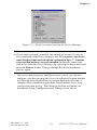
1
PCI-1712/1732 User's manual
1 MS/s, 12-bit, 16-ch HighSpeed Multifunction Card
PCI-1712/1732
Quick
Start
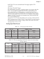
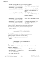
Unpacking
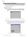
Hardware Installation
The PCI-1712/1732 package should contain the
following items:
Step 1: Turn off your computer and unplug the
power cord and cables
þ
þ
þ
þ
Step 2: Remove the cover of your computer
PCI-1712/1732 card
Companion CD-ROM disc
User’s Manual
Quick Start
Driver Installation
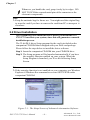
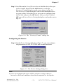
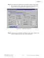
Step 1: Insert the companion disc into your CDROM drive.
Step 2: The Setup Program will be launched
automatically, and you’ll see the following
Setup Screen.
Select the DLL Drivers installation option.
(If autoplay is not enabled, please use
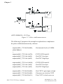
Step 3: Remove the slot cover on the back panel
of your computer
Step 4: Touch the metal part of your computer
chassis to discharge static electricity on
your body
Step 5: Insert the PCI-1712/1732 card into a PCI
slot. Hold the card only by its edges and
carefully align it with the slot, then insert
the card firmly into place. Use of
excessive force must be avoided otherwise
the card might be damaged.
Step 6: Fasten the bracket of the PCI card on the
back panel rail of the computer with
screws
Step 7: Connect appropriate accessories (68-pin
cable, wiring terminals, etc., if necessary)
to the PCI card.
Step 8: Replace the cover of your computer
chassis. Re-connect the cables you
removed in step 2.
Step 9:Plug in the power cord and turn on the
computer
Verifying your Installation
Windows Explorer or Windows Run
command to execute setup.exe on CDROM).
Step 3: Select the Windows 95/98 or Windows
NT option according to your operating
system.
Step 4: Follow the installation instructions step
by step to complete your DLL driver
setup.
w Access the Device Manager through the Control
Panel/System/Device Manager. On the Device
Manager tab of the System Property sheet, you
can see the Device Name of the PCI-1712/1732
listed on it.
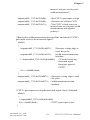
Device Installation
Step 1: Run the Device Installation program (by
accessing Start/Programs/ Advantech
Driver for 95 and 98 (or for NT)/Device
Installation).
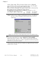
Step 2: On the Device Installation program
window, select the Device menu item on
the menu bar, and click the Setup
command to bring up the I/O Device
Installation dialog box as below:
Step 6: After your card is properly installed and
configured, you can click the Test button
to test your hardware.
Step 7: You can test your hardware by using the
testing utility we supplied. For more
detailed information, please refer to
Chapter 2 of the User’s Manual .
Step 3: Scroll down the List of Devices box to find
the device that you wish to configure,
then click the Add button to bring up the
Device Found(s) dialog box as shown
below:
Step 4: After selecting a device and click OK, the
Device Setting dialog box will pop up.
You can configure various settings for the
selected device.
Step 5: After you have finished configuring of the
device, click OK and the device will
appear in the Installed Devices box as
seen below:
Copyright®
This documentation and the software included with this product are
copyrighted 2000 by Advantech Co., Ltd. All rights are reserved.
Advantech Co., Ltd. reserves the right to make improvements in the
products described in this manual at any time without notice.
No part of this manual may be reproduced, copied, translated or
transmitted in any form or by any means without the prior written
permission of Advantech Co., Ltd. Information provided in this manual
is intended to be accurate and reliable. However, Advantech Co., Ltd.
assumes no responsibility for its use, nor for any infringements of the
rights of third parties which may result from its use.
Acknowledgments
PC-LabCard is a trademark of Advantech Co., Ltd. IBM and PC are
trademarks of International Business Machines Corporation. MS-DOS,
Windows®, Microsoft® Visual C++ and Visual BASIC are trademarks of
Microsoft® Corporation. Intel® and Pentium® are trademarks of Intel
Corporation. Delphi and C++Builder are trademarks of Inprise Corporation.
CE notification
The PCI-1712/1732, developed by ADVANTECH CO., LTD., has passed
the CE test for environmental specifications when shielded cables are
used for external wiring. We recommend the use of shielded cables.
This kind of cable is available from Advantech. Please contact your
local supplier for ordering information.
On-line Technical Support
Part No. 2003171200
1st Edition
Printed in Taiwan September 2000
Contents
1. Introduction ................................................................. 1
1.1
1.2
1.3
Features ......................................................................................... 1
Installation Guide ........................................................................... 3
Accessories ................................................................................... 5
2. Installation .................................................................. 7
2.1
2.2
2.3
2.4
2.5
Unpacking ...................................................................................... 7
Driver Installation .......................................................................... 8
Hardware Installation ..................................................................... 9
Device Setup & Configuration ..................................................... 12
Device Testing ............................................................................. 15
3. Signal Connections .................................................. 19
3.1
3.2
3.3
3.4
3.5
Overview ...................................................................................... 19
I/O Connector .............................................................................. 19
Analog Input Connections .......................................................... 24
Analog Output Connections ....................................................... 27
Field Wiring Considerations ........................................................ 28
4. Software Overview ................................................... 29
4.1
4.2
Programming Choices .................................................................. 29
DLL Driver Programming Roadmap ............................................. 30
5. Principles of Operation ............................................ 33
5.1
5.2
5.3
5.4
Analog Input Features ................................................................. 33
Analog Output Features .............................................................. 40
Digital I/O Features ...................................................................... 43
Counter/Timer Features ............................................................... 44
6. Calibration ................................................................. 55
6.1 VR Assignment ............................................................................... 55
6.2 A/D Calibration ............................................................................... 56
6.3 D/A Calibration ............................................................................... 57
6.4 Calibration Utility ............................................................................ 58
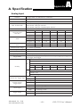
Appendix A. Specification............................................ 69
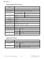
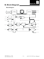
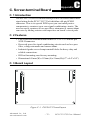
Appendix B. Block Diagram ........................................ 73
Appendix C. Screw-terminal Board............................. 75
C. 1
C. 2
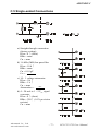
C. 3
C.4
C.5
C.6
Introduction ................................................................................. 75
Features ....................................................................................... 75
Board Layout ............................................................................... 75
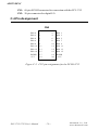
Pin Assignment ........................................................................... 76
Single-ended Connections ........................................................... 77
Differential Connections .............................................................. 78
Appendix D. Register Structure and Format .............. 79
D.1
D.2
D.3
D.4
D.5
D.6
D.7
D.8
D. 9
D.10
D.11
D.12
D.13
Overview ...................................................................................... 79
I/O Port Address Map ................................................................. 79
A/D Single Value Acquisition — Write BASE+0 ......................... 83
Channel and A/D data — Read BASE + 0 ................................... 83
A/D Channel Range Setting — Write BASE+2 ............................ 84
MUX Control — Write BASE+4 .................................................. 85
A/D Control/Status Register — Write/Read BASE+6 .................. 87
Clear interrupt and FIFO — Write BASE+8 ................................. 89
Interrupt and FIFO status — Read BASE+8 ................................ 90
D/A control/status register — Write/Read BASE+A .................. 91
D/A Channel 0/1 Data — Write BASE+C/E ................................. 93
82C54 Counter Chip 0 — Write/Read BASE+10 to 16 .................. 94
82C54 counter chip 1 — Write/Read BASE+18 to 1E ................... 95
D.14 Counter gate and clock control/status — Write/ Read BASE+20
to 26 ............................................................................................. 96
D.15 Digital I/O registers — Write/Read BASE+28 .............................. 99
D.16 Digital I/O configuration registers — Write/Read BASE+2A .... 100
D.17 Calibration command registers — Write BASE+2C ................... 100
D.18 D/A Channel Data for Continuous Output Operation Mode —
Write BASE+30 .......................................................................... 102
Figures
Figure 2-1: The Setup Screen of Advantech Automation Software ....... 8
Figure 2-2: Different options for Driver Setup ....................................... 9
Figure 2-3: The device name listed on the Device Manager ............... 11
Figure 2-4: The Advantech Device Installation utility program ............ 12
Figure 2-5: The I/O Device Installation dialog box .............................. 12
Figure 2-6: The Device(s) Found dialog box .................................... 13
Figure 2-7: The Device Setting dialog box ......................................... 13
Figure 2-8: The Device Name appearing on the list of devices box .... 14
Figure 2-9: Analog Input tab on the Device Test dialog box ............... 15
Figure 2-10: Analog Input tab on the Device Test dialog box ............... 16
Figure 2-11: Analog Output tab on the Device Test dialog box ............ 16
Figure 2-12: Digital Input tab on the Device Test dialog box ................ 17
Figure 2-13: Digital Output tab on the Device Test dialog box .............. 17
Figure 2-14: Digital output tab on the Device Test dialog box .............. 18
Figure 3-1: I/O connector pin assignments for the PCI-1712/1732 ..... 20
Figure 3-2: Single-ended input channel connection ........................... 24
Figure 3-3: Differential input channel connection - ground reference
signal source .................................................................. 25
Figure 3-4: Differential input channel connection - floating signal
source ............................................................................ 26
Figure 3-5: Analog output connections .............................................. 27
Figure 5-1: Post-Trigger Acquisition Mode ........................................ 35
Figure 5-2: Delay-Trigger Acquisition Mode ....................................... 35
Figure 5-3: About-Trigger Acquisition Mode ...................................... 36
Figure 5-4: Pre-Trigger Acquisition Mode .......................................... 37
Figure 5-5: PCI-1712/1732 Sample Clock Source ............................. 38
Figure 5-6: Frequency measurement ................................................ 49
Figure 6-1: PCI-1712/1732 VR1 & TP5 .............................................. 55
Figure 6-2: Selecting the device you want to calibrate ....................... 58
Figure 6-3: Warning message before start calibration ....................... 59
Figure 6-4: Auto A/D Calibration Dialog Box ..................................... 59
Figure 6-5: A/D Calibration Procedure 1 ............................................ 60
Figure 6-6: A/D Calibration Procedure 2 ............................................ 60
Figure 6-7: A/D Calibration Procedure 3 ............................................ 61
Figure 6-8: A/D Calibration is finished ............................................... 61
Figure 6-9: Range Selection in D/A Calibration ................................. 62
Figure 6-10: Calibrating D/A Channel 0 ............................................... 62
Figure 6-11: Calibrating D/A Channel 1 ............................................... 63
Figure 6-12: D/A Calibration is finished ............................................... 63
Figure 6-13: Selecting Input Rage in Manual A/D Calibration panel ..... 64
Figure 6-14: Adjusting registers .......................................................... 65
Figure 6-15: Selecting D/A Range and ................................................ 66
Figure 6-16: Selecting D/A Range and ................................................ 66
Figure 6-17: Adjusting registers .......................................................... 67
Figure C-1: PCLD-8712 board layout ................................................. 75
Figure C-2: CN2 pin assignments for the PCLD-8712 ........................ 76
Tables
Table 3-1:
Table 3-1:
Table 3-1:
Table 5-1:
Table 5-2:
Table 5-3:
I/O Connector Signal Description (Part 1) ........................ 21
I/O Connector Signal Description (Part 2) ........................ 22
I/O Connector Signal Description (Part 3) ........................ 23
Gains and Analog Input Range ........................................ 33
Analog Input Data Format ............................................... 39
The corresponding Full Scale values for various Input
Voltage Ranges ............................................................... 39
Table 5-4: Analog Output Data Format ............................................ 43
Table 5-5: The corresponding Full Scale values for various Output
Voltage Ranges ............................................................... 43
Table D-1: PCI-1712/1732 register format (Part 1) ............................ 80
Table D-1: PCI-1712/1732 register format (Part 2) ............................ 81
Table D-1: PCI-1712/1732 register format (Part 3) ............................ 82
Table D-2: Register for channel number and A/D data ...................... 83
Table D-3: Register for A/D channel range setting ............................ 84
Table D-4: Gain Codes for the PCI-1712/1732 .................................. 85
Table D-5: Register for multiplexer control ........................................ 85
Table D-6: Register for A/D control/status ........................................ 87
Table D-7: Analog Input Acquisition Mode ........................................ 88
Table D-8: Register for clear interrupt and FIFO ............................... 89
Table D-9: Register for interrupt and FIFO status ............................. 90
Table D-10: Register for D/A control ................................................... 91
Table D-11: Analog output operation mode ......................................... 92
Table D-12: Register for D/A channel 0/1 data ................................... 93
Table D-13: Register for 82C54 counter chip 0 ................................... 94
Table D-14: Register for 82C54 counter chip 1 ................................... 95
Table D-15: Register for counter gate and clock control/status ........... 96
Table D-16 : Table of Cn1 to Cn0 register ............................................ 96
Table D-17: Table of Gn1 to Gn0 register ............................................ 97
Table D-18: Table for CLK_SEL1 to CLK_SEL0 register ..................... 99
Table D-19:
Table D-20:
Table D-21:
Table D-22:
Table D-23:
Table D-24:
Register for Digital I/O ..................................................... 99
Register for digital I/O configuration ............................... 100
Register for digital I/O configuration ............................... 100
Register for calibration command .................................. 100
Calibration command .................................................... 101
Register for D/A channel data ....................................... 102
1
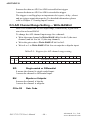
Chapter 1
Chapter
1. Introduction
Thank you for buying the Advantech PCI-1712/1732 PCI card. The
PCI-1712/1732 is a powerful high-speed multifunction DAS card for PCI
bus. It features a 1MHz 12-bit A/D converter, an on-board FIFO buffer
(storing up to 1K samples for A/D, and up to 32K samples for D/A
conversion). The PCI-1712/1732 provides a total of up to 16 singleended or 8 differential A/D input channels or a mixed combination, 2
12-bit D/A output channels, 16 digital input/output channels, and 3
10MHz 16-bit multifunction counter channels. PCI-1712/1732
provides specific functions for different user requirments:
PCI-1712 1 MS/s High-Speed Multifunction Card
PCI-1732 1 MS/s High-Speed Multifunction Card w/o analog output
The following sections of this chapter will provide further information
about features of the DAS card, a Quick Start for installation, together
with some brief information on software and accessories for the PCI1712/1732 card.
1.1 Features
The Advantech PCI-1712/1732 provides users with the most requested
measurement and control functions as seen below:
q PCI-bus mastering for data transfer
q 16 single-ended or 8 differential or combination analog inputs
q 12-bit A/D converter, with up to 1 MHz sampling rate
q Pre-, post-,about- and delay-trigger data acquisition modes for
analog input channels
q Programmable gain for each analog input channel
q Automatic channel/gain/SD/BU scanning
q On-board FIFO buffer storing up to 1K samples for A/D and 32K
samples for D/A
q Two 12-bit analog output channels with continuous waveform
output function
q Auto calibration for analog input and output channels
q 16 digital Input and output channels
q Three 16-bit programmable multifunction counters/timers on 10MHz
clock.
The Advantech PCI-1712 offers the following main features:
Advantech Co., Ltd.
www.advantech.com
–1–
PCI-1712/1732 User’s Manual
Chapter 1
PCI-Bus Mastering Data Transfer
The PCI-1712/1732 supports PCI-Bus mastering DMA for high-speed
data transfer and gap-free analog input and analog output. By setting
aside a block of memory in the PC, the PCI-1712/1732 performs busmastering data transfers without CPU intervention, setting the CPU
free to perform other more urgent tasks such as data analysis and
graphic manipulation. The function allows users to run all I/O functions simultaneously at full speed without losing data.
Plug-and-Play Function
The PCI-1712/1732 is a Plug-and-Play device, which fully complies with
the PCI Specification Rev 2.2. During card installation, you have no
need to set any jumpers or DIP switches. Instead, all bus-related
configurations such as base I/O address and interrupt are automatically done by the Plug-and-Play function.
On-board FIFO Memory
The PCI-1712/1732 provides an on-board FIFO (First In First Out)
memory buffer, storing up to 1K samples for A/D and 32K for D/A
conversion (PCI-1712 only).
Automatic Channel/Gain/SD*/BU* Scanning
PCI-1712/1732 features an automatic channel/Gain/SD/BU scanning
circuit. This circuit controls multiplexer switching during sampling in a
way that is much more efficient than software implementation. Onboard SRAM stores different gain, SD and BU values for each channel.
This combination lets user perform multi-channel high-speed sampling
with different gain, SD and BU values for each channel.
SD: Single-Ended/Differential Analog Input
BU: Bipolar/Unipolar
Flexible Triggering and Clocking Capabilities
The PCI-1712/1732 provides flexibility in triggering action, both in the
available trigger modes and trigger events for analog input. You can
acquire data using post-trigger, pre-trigger, delay-trigger and abouttrigger modes. The trigger source could be either analog or digital
signal. The analog trigger could originate from a dedicated input pin.
In fact, you can designate any of the analog input channels as the
analog trigger input. You can also set the analog trigger level within a
voltage range from zero to A/D FSR. When trigger signal being digital,
you can pace A/D and D/A conversion using software interrupt,
internal or external clock.
PCI-1712/1732 User’s Manual
–2–
Advantech Co., Ltd.
www.advantech.com
Chapter 1
Continuous Analog Output
The PCI-1712 provides two analog output channels. Both of them can
perform continuous waveform output. The analog output can be up to
500kS/s for each analog output channel. Or you can load a cyclic
waveform into an on-board FIFO, which will continuously output the
cyclic waveform. The on-board FIFO of the PCI-1712 can store 2 to 32K
samples for the waveform output.
On-board Programmable Multifunction Counter/Timer
The PCI-1712/1732 is equipped with three programmable multifunction
counters/timers, which can serve as a pacer trigger for A/D conversion. The counter chip is an 82C54 or equivalent, which incorporates
three 16-bit channels on a 10 MHz clock. And then we enhance the
gate and clock input function for more applications, of event counting,
pulse generation, duty cycle frequency generation, one shot, frequency measurement and pulse width measurement.
Note:
✎ Pace trigger determines how fast A/D conversion will be done in pacer
trigger mode.
✎ For detailed specifications of the PCI-1712/1732, please refer to Appendix A, Specifications.
1.2 Installation Guide
Before you install your PCI-1712/1732 card, please make sure you have
the following necessary components:
q PCI-1712/1732 DAS card
q PCI-1712/1732 User’s Manual
q Driver software
Advantech DLL drivers
(included in the companion CD-ROM)
q Wiring cable
PCL-10168
q Wiring board
PCLD-8712, ADAM-3968
q Computer
Personal computer or workstation with a
PCI-bus slot
Some other optional components are also available for enhanced
operation:
Advantech Co., Ltd.
www.advantech.com
–3–
PCI-1712/1732 User’s Manual
Chapter 1
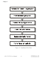
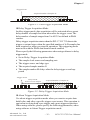
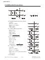
Figure 1-1: Installation Flow Chart
PCI-1712/1732 User’s Manual
–4–
Advantech Co., Ltd.
www.advantech.com
Chapter 1
q Application software ActiveDAQ, GeniDAQ or other third-party
software packages
After you have got the necessary components and maybe some
accessories for enhanced operation of your DAS card, you can then
begin the Installation procedures. Figure 1-1 on the next page provides a concise flow chart to give users a broad picture of the software
and hardware installation procedures:
1.3 Accessories
Advantech offers a complete set of accessory products to support the
PCI-1712/1732 cards. These accessories include:
Wiring Cable
q PCL-10168 The PCL-10168 shielded cable is specially designed
for PCI-1712/1732 card to provide higher resistance to noise. To
achieve a better signal quality, the signal wires are twisted in such a
way as to form a twisted-pair cable, reducing crosstalk and noise
from other signal sources. Furthermore, its analog and digital lines
are separately sheathed and shielded to neutralize EMI/EMC
problems.
Wiring Boards
q ADAM-3968 The ADAM-3968 is a 68-pin SCSI wiring terminal
module for DIN-rail mounting. This terminal module can be readily
connected to the Advantech PC-Lab cards and allow easy yet
reliable access to individual pin connections for the PCI-1712/1732
card.
qPCLD-8712 The PCLD-8712 is a DIN-rail mounting screwterminal board to be used with any of the PC-LabCards which have
68-pin SCSI connectors. The PCLD-8712 features the following
functions:
l One additional 20-pin flat-cable connectors for digital input and
output
l Reserved space on the board to meet future needs for signalconditioning circuits (low-pass filter, voltage attenuator and
current shunt)
Advantech Co., Ltd.
www.advantech.com
–5–
PCI-1712/1732 User’s Manual
Chapter 1
l
Industrial-grade screw-clamp terminal blocks for heavy-duty and
reliable connections.
PCI-1712/1732 User’s Manual
–6–
Advantech Co., Ltd.
www.advantech.com
2
Chapter 1
Chapter
2. Installation
This chapter gives users a package item checklist, proper instructions
about unpacking and step-by-step procedures for both driver and card
installation.
2.1 Unpacking
After receiving your PCI-1712/1732 package, please inspect its
contents first. The package should contain the following items:
þ PCI-1712/1732 card
þ Companion CD-ROM (DLL driver included)
þ User’s Manual
þ Quick Start
The PCI-1712/1732 card harbors certain electronic components
vulnerable to electrostatic discharge (ESD). ESD could easily damage
the integrated circuits and certain components if preventive measures
are not carefully paid attention to. Before removing the card from the
antistatic plastic bag, you should take following precautions to ward
off possible ESD damage:
l Touch the metal part of your computer chassis with your hand
to discharge static electricity accumulated on your body. Or one
can also use a grounding strap.
l
Touch the antistatic bag to a metal part of your computer
chassis before opening the bag.
l Take hold of the card only by the metal bracket when removing it
out of the bag.
After taking out the card, first you should:
l
Inspect the card for any possible signs of external damage
(loose or damaged components, etc.). If the card is visibly
damaged, please notify our service department or our local sales
representative immediately. Avoid installing a damaged card into
your system.
Also pay extra caution to the following aspects to ensure proper
installation:
Avoid physical contact with materials that could hold static
electricity such as plastic, vinyl and Styrofoam.
Advantech Co., Ltd.
www.advantech.com
–7–
PCI-1712/1732 User’s Manual
Chapter 2
Whenever you handle the card, grasp it only by its edges. DO
NOT TOUCH the exposed metal pins of the connector or the
electronic components.
Note:
✎ Keep the antistatic bag for future use. You might need the original bag
to store the card if you have to remove the card from PC or transport it
elsewhere.
2.2 Driver Installation
We recommend you to install the driver before you install the PCI1712/1732 card into your system, since this will guarantee a smooth
installation process.
The 32-bit DLL driver Setup program for the card is included on the
companion CD-ROM that is shipped with your DAS card package.
Please follow the steps below to install the driver software:
Step 1: Insert the companion CD-ROM into your CD-ROM drive.
Step 2: The Setup program will be launched automatically if you have
the autoplay function enabled on your system. When the
Setup Program is launched, you’ll see the following Setup
Screen.
Note:
✎ If the autoplay function is not enabled on your computer, use Windows
Explorer or Windows Run command to execute SETUP.EXE on the
companion CD-ROM.
Figure 2-1: The Setup Screen of Advantech Automation Software
PCI-1712/1732 User’s Manual
–8–
Advantech Co., Ltd.
www.advantech.com
Chapter 2
Step 3: Select the DLL Drivers option.
Step 4: Select the Windows 95/98 or Windows NT option according
to your operating system. Just follow the installation instructions step by step to complete your DLL driver setup.
Figure 2-2: Different options for Driver Setup
For further information on driver-related issues, an online version of
DLL Drivers Manual is available by accessing the following path:
Start/Programs/Advantech Driver for 95 and 98 (or for NT)/Driver
Manual
2.3 Hardware Installation
Note:
✎ Make sure you have installed the driver first before you install the card
(please refer to 2.2 Driver Installation)
After the DLL driver installation is completed, you can now go on to
install the PCI-1712/1732 card in any PCI slot on your computer. But it
is suggested that you should refer to the computer user manual or
related documentations if you have any doubt. Please follow the steps
below to install the card on your system.
Step 1: Turn off your computer and unplug the power cord and cables.
TURN OFF your computer before installing or removing any
components on the computer.
Advantech Co., Ltd.
www.advantech.com
–9–
PCI-1712/1732 User’s Manual
Chapter 2
Step 2: Remove the cover of your computer.
Step 3: Remove the slot cover on the back panel of your computer.
Step 4: Touch the metal part on the surface of your computer to
neutralize the static electricity that might be on your body.
Step 5: Insert the PCI-1712/1732 card into a PCI slot. Hold the card only
by its edges and carefully align it with the slot. Insert the card
firmly into place. Use of excessive force must be avoided,
otherwise the card might be damaged.
Step 6: Fasten the bracket of the PCI card on the back panel rail of the
computer with screws.
Step 7: Connect appropriate accessories (68-pin cable, wiring terminals, etc. if necessary) to the PCI card.
Step 8: Replace the cover of your computer chassis. Re-connect the
cables you removed in step 2.
Step 9: Plug in the power cord and turn on the computer .
Note:
✎ In case you installed the card without installing the DLL driver first,
Windows 95/98 will recognize your card as an “unknown device” after
reboot, and will prompt you to provide necessary driver. You should
ignore the prompting messages (just click the Cancel button) and set
up the driver according to the steps described in 2.2 Driver Installation.
After the PCI-1712/1732 card is installed, you can verify whether it is
properly installed on your system in the Device Manager:
1. Access the Device Manager through Control Panel/System/Device
Manager.
2. The device name of the PCI-1712/1732 should be listed on the
Device Manager tab on the System Property Page.
PCI-1712/1732 User’s Manual
– 10 –
Advantech Co., Ltd.
www.advantech.com
Chapter 2
Figure 2-3: The device name listed on the Device Manager
Note:
✎ If your card is properly installed, you should see the device name of
your card listed on the Device Manager tab. If you do see your device
name listed on it but marked with an exclamation sign “!” , it means
your card has not been correctly installed. In this case, remove the
card device from the Device Manager by selecting its device name and
press the Remove button. Then go through the driver installation
process again.
After your card is properly installed on your system, you can now
configure your device using the Device Installation Program that has
itself already been installed on your system during driver setup. A
complete device installation procedure should include device setup,
configuration and testing. The following sections will guide you
through the Setup, Configuration and Testing of your device.
Advantech Co., Ltd.
www.advantech.com
– 11 –
PCI-1712/1732 User’s Manual
Chapter 2
2.4 Device Setup & Configuration
The Device Installation program is a utility that allows you to set up,
configure and test your device, and later stores your settings on the
system registry. These settings will be used when you call the APIs of
Advantech 32-bit DLL drivers.
Setting Up the Device
Step 1: To install the I/O device for your card, you must first run the
Device Installation program (by accessing Start/Programs/
Advantech Driver for 95 and 98 (or for NT)/Device Installation).
Figure 2-4: The Advantech Device Installation utility program
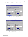
Step 2: On the Device Installation program window, select the Device
menu item on the menu bar, and click the Setup command (Fig.
2-4) to bring up the I/O Device Installation dialog box (Fig. 25). You can then view the device(s) already installed on your
system (if any) on the Installed Devices list box.
Figure 2-5: The I/O Device Installation dialog box
PCI-1712/1732 User’s Manual
– 12 –
Advantech Co., Ltd.
www.advantech.com
Chapter 2
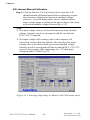
Step 3: Scroll down the List of Devices box to find the device that you
wish to install, then click the Add button to evoke the
Device(s) Found dialog box such as one shown in Fig. 2-6.
The Device(s) Found dialog box lists all the installed devices
on your system. Select the device you want to configure from
the list box and press the OK button. After you have clicked
OK, you will see a Device Setting dialog box such as the one in
Fig. 2-7.
Figure 2-6: The “Device(s) Found” dialog box
Configuring the Device
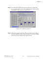
Step 4: On the Device Setting dialog box (Fig. 2-7), you can configure
the parameters of A/D, D/A, DIO and Counter functions.
Figure 2-7: The Device Setting dialog box
Note:
✎Users can configure the source of D/A reference voltage either as
Internal or External, and then select for the unipolar or the bipolar
Advantech Co., Ltd.
www.advantech.com
– 13 –
PCI-1712/1732 User’s Manual
Chapter 2
output voltage range. When selecting voltage source as Internal,
users will have options for the output voltage ranges : 0 ~ 5V and 0 ~
10V for unipolar; -5 ~ 5V and -10 ~ 10V for bipolar.
When selected as External, the output voltage range is determined by
the external reference voltage in the following way :
By inputting an external reference voltage: xV, where 0<=x<=10,
you will get a output voltage range:
0 to xV for unipolar;
and -x to xV for bipolar
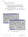
Step 5: After you have finished configuring the device, click OK and
the device name will appear in the Installed Devices box as
seen below:
Figure 2-8: The Device Name appearing on the list of devices box
Note:
✎ As we have noted, the device name “000:PCI-1712 I/O=6600H”
begins with a device number “000”, which is specifically assigned to
each card cifically. The device number is passed to the driver to specify
which device you wish to control.
If you want to test the card device further, go right to the next section
on the Device Testing.
PCI-1712/1732 User’s Manual
– 14 –
Advantech Co., Ltd.
www.advantech.com
Chapter 2
2.5 Device Testing
Following through the Setup and Configuration procedures to the last
step described in the previous section, you can now proceed to test
the device by clicking the Test Button on the I/O Device Installation
dialog box (Fig. 2-8). A Device Test dialog box will appear accordingly:
Figure 2-9: Analog Input tab on the Device Test dialog box
On the Device Test dialog box, users are free to test various functions
of PCI-1712/1732 on the Analog input, Analog output, Digital input,
Digital output or Counter tabs.
Note:
✎You can access the Device Test dialog box either by the previous
procedure for the Device Installation Program or simply by accessing
Start/Programs/Advantech Driver for 95 and 98 (or for NT) /Test
Utility.
Testing Analog Input Function
Click the Analog Input tab to bring it up to front of the screen. Select
the input range for each channel in the Input range drop-down boxes.
Configure the sampling rate on the scroll bar. Switch the channels by
using the up/down arrow.
Advantech Co., Ltd.
www.advantech.com
– 15 –
PCI-1712/1732 User’s Manual
Chapter 2
Figure 2-10: Analog Input tab on the Device Test dialog box
Testing Analog Output Function (PCI-1712 only)
Click the Analog Output tab to bring it up to the foreground. The
Analog Output tab allows you to output quasi-sine, triangle, or square
waveforms generated by the software automatically, or output single
values manually. You can also configure the waveform frequency and
output voltage range.
Figure 2-11: Analog Output tab on the Device Test dialog box
Testing Digital Input Function
Click the Digital Input tab to show forth the Digital Input test panel
as seen below. Through the color of the lamps, users can easily discern
whether the status of each digital input channel is either high or low.
PCI-1712/1732 User’s Manual
– 16 –
Advantech Co., Ltd.
www.advantech.com
Chapter 2
Figure 2-12: Digital Input tab on the Device Test dialog box
Testing Digital Output Function
Click the Digital Output tab to bring up the Digital Output test panel
such as seen on the next page. By pressing the buttons on each tab,
users can easily set each digital output channel as high or low for the
corresponding port.
Figure 2-13: Digital Output tab on the Device Test dialog box
Testing Counter Function
Click the Counter Tab to bring its test panel forth. In the test utility,
the counter channel (Channel 0) offers the users two options: Event
counting and Pulse out. If you select Event counting, you need first to
connect your clock source to pin CNT0_CLK, and the counter will start
counting after the pin CNT0_GATE is triggered. If you select Pulse
Out, the clock source will be output to pin CNT0_OUT. You can
Advantech Co., Ltd.
www.advantech.com
– 17 –
PCI-1712/1732 User’s Manual
Chapter 2
configure the Pulse Frequency by the scroll bar right below it.
Figure 2-14: Digital output tab on the Device Test dialog box
Only after your card device is properly set up, configured and tested,
can the device installation procedure be counted as complete. After the
device installation procedure is completed, you can now safely proceed to the
next chpater, Signal Connections.
PCI-1712/1732 User’s Manual
– 18 –
Advantech Co., Ltd.
www.advantech.com
3
Chapter 3
3. Signal Connections
Chapter
3.1 Overview
Maintaining proper signal connections is one of the most important
factors to ensure that your application system is sending and receiving
data correctly. A good signal connection can avoid unnecessary and
costly damage to your PC and other hardware devices. This chapter
provides useful information about how to connect input and output
signals to the PCI-1712/1732 via the I/O connector.
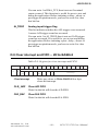
3.2 I/O Connector
The I/O connector on the PCI-1712/1732 is a 68-pin connector that
enables you to connect to accessories with the PCL-10168 shielded
cable.
Note:
✎ The PCL-10168 shielded cable is especially designed for the PCI-1712/
1732 to reduce noise in the analog signal lines. Please refer to Section
1.3 Accessories.
Pin Assignment
Figure 3-1 shows the pin assignments for the 68-pin I/O connector on
the PCI-1712/1732, and table 3-1 lists the detailed illustration of the
pins.
Note:
✎ The three ground references AIGND, AOGND, and DGND should be
used discreetly each according to its designated purpose.
Advantech Co., Ltd.
www.advantech.com
– 19 –
PCI-1712/1732 User’s Manual
Chapter 3
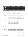
Figure 3-1: I/O connector pin assignments for the PCI-1712/1732
*: Pins 20, 22~25, 54, 56~59 are not defined on PCI-1732
PCI-1712/1732 User’s Manual
– 20 –
Advantech Co., Ltd.
www.advantech.com
Chapter 3
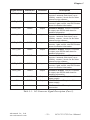
I/O Connector Signal Description
Signal Name
Reference
Direction
Description
AI<0...15>
AIGND
Input
Analog Input Channels 0 through 15.
Each channel pair, AI<i, i+8> (i = 0...7),
can be configured as either one
differential input or two single-ended
inputs.
AIGND
-
-
Analog Input Ground. These pins are
the reference points for single-ended
measurements and the bias current
return point for differential
measurement. All three ground
references ? AIGND, AOGND and
DGND ? are connected together on
the PCI-1712 card.
AO0_REF
AOGND
Input
Analog Channel 0 Output External
Reference. This is the external
reference input for the analog output
channel 0 circuitry.
AO1_REF
AOGND
Input
Analog Channel 1 Output External
Reference. This is the external
reference input for the analog output
channel 1 circuitry.
ANA_TRG
AIGND
Input
Analog threshold Trigger. This pin is
the analog input threshold trigger input.
AO0_OUT
AOGND
Output
Analog Channel 0 Output. This pin
supplies the voltage output of analog
output channel 0.
AO1_OUT
AOGND
Output
Analog Channel 1 Output. This pin
supplies the voltage output of analog
output channel 1.
AI_CLK
DGND
Input
Analog Input external clock input.
This is the external clock input for the
analog input.
AI_TRG
DGND
Input
Analog Input TTL Trigger-This is the
TTL trigger for analog trigger.
AOGND
-
-
Analog Output Ground. The analog
output voltages are referenced to
theses nodes. All three ground
references ? AIGND, AOGND, and
DGND ? are connected together on
your PCI-1712 card.
Table 3-1: I/O Connector Signal Description (Part 1)
Advantech Co., Ltd.
www.advantech.com
– 21 –
PCI-1712/1732 User’s Manual
Chapter 3
Signal Name
Reference
Direction
Description
DIO<0..15>
DGND
Input
Digital Input / Output signals. These
pins are digital input / output channel 0
to 15
AI_CLK
DGND
Input
Analog Input external clock input.
This is the external clock input for the
analog input.
AI_TRG
DGND
Input
Analog Input TTL Trigger- This is the
TTL trigger for analog trigger.
AI_CLK_OUT
DGND
Output
Analog Input Clock Output. This pin
pulses once for each pacer clock. This
signal serves as a synchronous signal
for application. The low-to-high edge
start A/D conversion.
AI_TRG_OUT
DGND
Output
Analog Input Trigger Output. This pin
outputs the analog input trigger signal.
The low-to-high edge indicates the
trigger event.
DGND
-
-
Digital Ground. This pin supplies the
reference for the digital signals at the
I/O connector as well as the +5VDC
supply. All three ground references ?
AIGND, AOGND, and DGND ? are
connected together on your PCI-1712
card.
Table 3-1: I/O Connector Signal Description (Part 2)
PCI-1712/1732 User’s Manual
– 22 –
Advantech Co., Ltd.
www.advantech.com
Chapter 3
Signal Name
Reference
Direction
Description
CNT0_CLK
DGND
Input
Counter 0 Clock Input. This pin is the
counter 0 external clock input (up to
10MHz), counter 0 clock can be either
internal set by software.
CNT0_GATE
DGND
Input
Counter 0 Gate Input. This pin is for
counter 0 gate control, see 82C54 data
sheet for detailed information.
CNT0_OUT
DGND
Output
Counter 0 Output. This pin is counter
0 output, see 82C54 data sheet for
detailed information.
CNT1_CLK
DGND
Input
Counter 1 Clock Input. This pin is the
counter 1 external clock input (up to
10MHz), counter 1 clock can be either
internal set by software.
CNT1_GATE
DGND
Input
Counter 1 Gate Input. This pin is for
counter 1 gate control, see 82C54 data
sheet for detailed information.
CNT1_OUT
DGND
Output
Counter 1 Output. This pin is counter
1 output, see 82C54 data sheet for
detailed information.
CNT2_CLK
DGND
Input
Counter 2 Clock Input. This pin is the
counter 2 external clock input (up to
10MHz), counter 2 clock can be either
internal set by software.
CNT2_GATE
DGND
Input
Counter 2 Gate Input. This pin is for
counter 2 gate control, see 82C54 data
sheet for detailed information.
CNT2_OUT
DGND
Output
Counter 2 Output. This pin is counter
2 output, see 82C54 data sheet for
detailed information.
+12V
DGND
Output
+12 VDC Source. This pin is +12V
power supply.
+5V
DGND
Output
+5 VDC Source. This pin is +5 V
power supply.
NC
-
-
No Connection. These pins serve no
connection.
Table 3-1: I/O Connector Signal Description (Part 3)
Advantech Co., Ltd.
www.advantech.com
– 23 –
PCI-1712/1732 User’s Manual
Chapter 3
3.3 Analog Input Connections
The PCI-1712/1732 supports either 16 single-ended or 8 differential
analog inputs. Each individual input channel is software-selected.
Single-ended Channel Connections
The single-ended input configuration has only one signal wire for each
channel, and the measured voltage (Vm) is the voltage of the wire as
referenced against the common ground.
A signal source without a local ground is also called a “floating
source”. It is fairly simple to connect a single-ended channel to a
floating signal source. In this mode, the PCI-1712/1732 provides a
reference ground for external floating signal sources.
Figure 3-2 shows a single-ended channel connection between a
floating signal source and an input channel on the PCI-1712/1732.
Figure 3-2: Single-ended input channel connection
Differential Channel Connections
The differential input channels operate with two signal wires for each
channel, and the voltage difference between both signal wires is
measured. On the PCI-1712/1732, when all channels are configured to
differential input, up to 8 analog channels are available.
If one side of the signal source is connected to a local ground, the
signal source is ground-referenced. Therefore, the ground of the
signal source and the ground of the card will not be exactly of the
PCI-1712/1732 User’s Manual
– 24 –
Advantech Co., Ltd.
www.advantech.com
Chapter 3
same voltage. The difference between the ground voltages forms a
common-mode voltage (Vcm).
To avoid the ground loop noise effect caused by common-mode
voltages, you can connect the signal ground to the Low input. Figure
3-3 shows a differential channel connection between a groundreference signal source and an input channel on the PCI-1712/1732.
With this connection, the PGIA rejects a common-mode voltage Vcm
between the signal source and the PCI-1712/1732 ground, shown as
Vcm in Figure 3-3.
Figure 3-3: Differential input channel connection - ground reference
signal source
If a floating signal source is connected to the differential input
channel, the signal source might exceed the common-mode signal
range of the PGIA, and the PGIA will be saturated with erroneous
voltage-readings. You must therefore reference the signal source
against the AIGND.
Figure 3-4 shows a differential channel connection between a floating
signal source and an input channel on the PCI-1712/1732. In this
figure, each side of the floating signal source is connected through a
resistor to the AIGND. This connection can reject the common-mode
voltage between the signal source and the PCI-1712/1732 ground.
Advantech Co., Ltd.
www.advantech.com
– 25 –
PCI-1712/1732 User’s Manual
Chapter 3
Figure 3-4: Differential input channel connection - floating signal
source
However, this connection has the disadvantage of loading the source
down with the series combination (sum) of the two resistors. For ra and
rb, for example, if the input impedance rs is 1 kΩ, and each of the two
resistors is 100 kW, then the resistors load down the signal source with
200 kΩ (100 kΩ + 100 kΩ), resulting in a –0.5% gain error. The following
gives a simplified representation of the circuit and calculating process.
PCI-1712/1732 User’s Manual
– 26 –
Advantech Co., Ltd.
www.advantech.com
Chapter 3
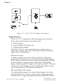
3.4 Analog Output Connections
The PCI-1712 provides two D/A output channels, AO0_OUT and
AO1_OUT. Users may use the PCI-1712 internally-provided precision
+5V (+10V) reference to generate 0 ~ +5 V and 0 ~ +10 V unipolar D/A
output range; or to generate -5 ~ +5 V and -10 ~ +10 V for bipolar
output range.
Users may also set D/A output range through external references,
AO0_REF and AO1_REF. The external reference input range is 0~10
V. For example, connecting with an external reference of +7 V will
generate 0 ~ +7 V D/A output for unipolar; and -7 ~ +7 V for bipolar.
Figure 3-5 shows how to make analog output and external reference
input connections on the PCI-1712.
Internal
+5V
+10V
External
AO0_REF
INT_REF
AO0
+
AO0_OUT
Load
_
Load
_
External Reference
For DA Signal 0
AOGND
DATA BUS
AO1
External Reference
For DA Signal 1
AO1_OUT
+
AO1_REF
INT_REF
I/O Connector
Figure 3-5: Analog output connections
Advantech Co., Ltd.
www.advantech.com
– 27 –
PCI-1712/1732 User’s Manual
Chapter 3
3.5 Field Wiring Considerations
When you use the PCI-1712/1732 to acquire data from outside, noises
in the environment might significantly affect the accuracy of your
measurements if due cautions are not taken. The following measures
will be helpful to reduce possible interference running signal wires
between signal sources and the PCI-1712/1732.
• The signal cables must be kept away from strong electromagnetic sources such as power lines, large electric motors, circuit
breakers or welding machines, since they may cause strong
electromagnetic interference. Keep the analog signal cables
away from any video monitor, since it can significantly affect
data acquisition system.
• If the cable travels through area with significant electromagnetic
interference, you should adopt individually shielded, twistedpair wires as the analog input cable. This type of cable have its
signal wires twisted together and shielded with a metal mesh.
The metal mesh should only be connected to one point at the
signal source ground.
• Avoid running the signal cables through any conduit that might
have power lines in it.
• If you have to place your signal cable parallel to a power line
that has a high voltage or high current running through it, try to
keep a safe distance between them. Or you should place the
signal cable at right angle to the power line to minimize the
undesirable effect.
• The signals transmitted on the cable will be directly affected by
the quality of the cable. In order to ensure best signal quality, we
recommend that you use the PCL-10168 shielded cable.
PCI-1712/1732 User’s Manual
– 28 –
Advantech Co., Ltd.
www.advantech.com
4
Chapter 4
4. Software Overview
Chapter
This chapter gives you an overview of the software programming
choices available and a quick reference to source codes examples that
can help you be better oriented to programming. After following the
instructions given in Chapter 2, it is hoped that you feel comfortable
enough to proceed further.
Programming choices for DAS cards: You may use Advantech
application software such as Advantech DLL driver. On the other
hand, advanced users are allowed another option for register-level
programming, although not recommended due to its laborious and
time-consuming nature.
4.1 Programming Choices
DLL Driver
The Advantech DLL Drivers software is included on the companion
CD-ROM at no extra charge. It also comes with all the Advantech DAS
cards. Advantech’s DLL driver features a complete I/O function library
to help boost your application performance. The Advantech DLL
driver for Windows 95/98/NT works seamlessly with development
tools such as Visual C++, Visual Basic, Inprise C++ Builder and Inprise
Delphi.
Register-level Programming
Register-level programming is reserved for experienced programmers
who find it necessary to write codes directly at the level of device
registers. Since register-level programming requires much effort and
time, we recommend that you use the Advantech DLL drivers instead.
However, if register-level programming is indispensible, you should
refer to the relevant information in Appendix C, Register Structure and
Format, or to the example codes included on the companion CD-ROM.
Advantech Co., Ltd.
www.advantech.com
– 29 –
PCI-1712/1732 User’s Manual
Chapter 4
4.2 DLL Driver Programming Roadmap
This section will provide you a roadmap to demonstrate how to build
an application from scratch using Advantech DLL driver with your
favorite development tools such as Visual C++, Visual Basic, Delphi
and C++ Builder. The step-by-step instructions on how to build your
own applications using each development tool will be given in the DLL
Drivers Manual. Moreover, a rich set of example source codes are also
given for your reference.
Programming Tools
Programmers can develop application programs with their favorite
development tools:
q Visual C++
q Visual Basic
q Delphi
q C++ Builder
For instructions on how to begin programming works in each development tool, Advantech offers a Tutorial Chapter in the DLL Drivers
Manual for your reference. Please refer to the corresponding sections
in this chapter on the DLL Drivers Manual to begin your programming
efforts. You can also take a look at the example source codes provided
for each programming tool, since they can get you very well-oriented.
The DLL Drivers Manual can be found on the companion CD-ROM.
Or if you have already installed the DLL Drivers on your system, The
DLL Drivers Manual can be readily accessed through the Start
button:
Start/Programs/Advantech Driver for 95 and 98 (or for NT)/Driver
Manual
The example source codes could be found under the corresponding
installation folder such as the default installation path:
\Program Files\Advantech\ADSAPI\Examples
For information about using other function groups or other development tools, please refer to the Creating Windows 95/NT Application
with DLL Driver chapter and the Function Overview chapter on the
DLL Drivers Manual.
PCI-1712/1732 User’s Manual
– 30 –
Advantech Co., Ltd.
www.advantech.com
Chapter 4
Programming with DLL Driver Function Library
Advanech DLL driver offers a rich function library to be utilized in
various application programs. This function library consists of
numerous APIs that support many development tools, such as Visual
C++, Visual Basic, Delphi and C++ Builder.
According to their specific functions or sevices, those APIs can be
categorized into several function groups:
q Analog Iutput Function Group
q Analog Output Function Group
q Digital Input/Output Function Group
q Counter Function Group
q Temperature Measurement Function Group
q Alarm Function Group
q Port Function Group
q Communication Function Group
q Event Function Group
For the usage and parameters of each function, please refer to the
Function Overview chapter in the DLL Drivers Manaul.
Troubleshooting DLL Driver Error
Driver functions will return a status code when they are called to
perform a certain task for the application. When a function returns a
code that is not zero, it means the function has failed to perform its
designated function. To troubleshoot the DLL driver error, you can
pass the error code to DRV_GetErrorMessage function to return the
error message. Or you can refer to the DLL Driver Error Codes
Appendix in the DLL Drivers Manaul for a detailed listing of the Error
Code, Error ID and the Error Message.
Advantech Co., Ltd.
www.advantech.com
– 31 –
PCI-1712/1732 User’s Manual
Chapter 4
PCI-1712/1732 User’s Manual
– 32 –
Advantech Co., Ltd.
www.advantech.com
5
Chapter 4
5. Principles of Operation
Chapter
This chapter describes the analog input, analog output, digital I/O and
counter/timer features of the PCI-1712/1732 card.
5.1 Analog Input Features
This section describes the following features of the analog input (A/D)
of PCI-1712/1732 card:
w Analog input ranges and gains
w Analog input acquisition modes
w A/D sample clock sources
w Trigger sources
w Analog Input Data Format
Analog Input Ranges and Gains
Each channel on the PCI-1712/1732 can measure unipolar and bipolar
analog input signals. A unipolar signal can range between 0 to 10 V
FSR, while a bipolar signal extends within ± 10 V FSR.
The PCI-1712/1732 is able to set different input ranges for each
channel. When the channels are set as unipolar or bipolar input in FSR,
the sampling rate can be up to 600 kS/s, but when there is a mixed
combination of unipolar and bipolar inputs, it can operate only with a
rate up to 400 kS/s.
The PCI-1712/1732 also provides various gain levels that are programmable per channel. Table 5-1 lists the effective ranges supported by the
PCI-1712/1732 using these gains.
Table 5-1: Gains and Analog Input Range
Gain
Unipolar Analog Input Range
Bipolar Analog Input Range
0.5
N/A
± 10 V
1
0 ~ 10 V
± 5V
2
0~5V
± 2.5 V
4
0 ~ 2.5 V
± 1.25 V
8
0 ~ 1.25 V
± 0.625 V
For each channel, choose the gain level that provides most optimal
range that can accommodate the signal range you have to measure. For
detailed information, please refer to Appendix D.5 A/D Channel Range
Setting.
Advantech Co., Ltd.
www.advantech.com
– 33 –
PCI-1712/1732 User’s Manual
Chapter 5
Analog Input Acquisition Modes
The PCI-1712/1732 can acquire data in single value, pacer, post-trigger,
delay-trigger, about-trigger and pre-trigger acquisition modes. These
analog input acquisition modes are described in more detail in the
followings:
q Single Value Acquisition Mode
The single value acquisition mode is the simplest way to acquire data.
Once the software issues a trigger command, the A/D converter will
convert one data, and return it immediately. User can check the A/D
FIFO status (A/D_F/E on Read BASE+8) to make sure if the data is
ready to be received. For detailed information, please refer to Appendix
D.9 Interrupt and FIFO status.
q Pacer Acquisition Mode
Use pacer acquisition mode to acquire data if you want to accurately
control the time interval between conversions of individual channels in
a scan. A/D conversion clock comes from A/D counter or external
AI_CLK on connector. A/D conversion starts when the first clock
signal comes in, and will not stop if the clock is still continuously
sending into it. Conversion data is put into the A/D FIFO. For highspeed data acquisition, you have to use the DMA data transfer for
analog input to prevent data loss.
q Post-Trigger Acquisition Mode
Post-trigger allows you to acquire data based on a trigger event. Posttrigger acquisition starts when the PCI-1712/1732 detects the trigger
event and stops when the preset number of post-trigger samples has
been acquired or when you stop the operation. This trigger mode must
work with the DMA data transfer mode enabled.
Use post-trigger acquisition mode when you want to acquire data
when a post-trigger event occurs. Please specify the following
parameters when using software in post-trigger acquisition mode:
w Set to Post-Trigger Acquisition Mode
w The A/D sample clock source and sampling rate
w The trigger source and edge type
w The acquired sample number N
PCI-1712/1732 User’s Manual
– 34 –
Advantech Co., Ltd.
www.advantech.com
Chapter 5
Trigger Event
Acquired number of samples N
1st 2nd 3rd
N-2th N-1th Nth
t
Figure 5-1: Post-Trigger Acquisition Mode
q Delay Trigger Acquisition Mode
In delay trigger mode, data acquisition will be activated after a preset
delay number of sample has been taken after the trigger event. The
delay number of sample ranges from 2 to 65535 as defined in DMA
counter.
Delay-trigger acquisition starts when the PCI-1712/1732 detects the
trigger event and stops when the specified number of A/D samples has
been acquired or when you stop the operation. This triggering mode
must work with the DMA data transfer mode enabled
Please specify the following parameters when using software in delay
trigger mode:
w Set to Delay-Trigger Acquisition Mode
w The sample clock source and sampling rate
w The trigger source and edge type
w The acquired sample number N
w The sample number M delays after the delay-trigger event happened
Trigger Event
Delay time M:
from 2 to 65535 samples
1
2
3
M-2 M-1 M
Acquired number of samples N
1st 2nd 3rd
N-2 N-1 N
t
Figure 5-2: Delay-Trigger Acquisition Mode
q About Trigger Acquisition Mode
Use about-trigger acquisition mode when you want to acquire data
both before and after a specific trigger event occurs. This operation is
equivalent to doing both a pre-trigger and a post-trigger acquisition.
When using software, please specify the following parameters, when
using software in About-Trigger acquisition mode:
Advantech Co., Ltd.
www.advantech.com
– 35 –
PCI-1712/1732 User’s Manual
Chapter 5
w
w
w
w
w
Set to About-Trigger Acquisition Mode
The sample clock source and sample rate
The trigger source and edge type
The total acquired sample number N
The specific sample number M before the trigger event. The range
of preset sample number is 2 samples minimum and is limited on
basis of memory size of your host PC.
In about-trigger mode, users must first designate the size of the
allocated memory and the amount of samples to be snatched after the
trigger event happens. The about-trigger acquisition starts when the
first clock signal comes in. Once a trigger event happens, the on-going
data acquisition will continue until the designated amount of samples
have been reached. When the PCI-1712/1732 detects the selected
about-trigger event, the card keeps acquiring the preset number of
samples, and kept the total number of samples on the FIFO.
Trigger Event
Acquired number of
samples M after trigger
event happened
1
2
N-M
3
N
t
Total Acquired sample number: N
Figure 5-3: About-Trigger Acquisition Mode
q Pre-Trigger Acquisition Mode
Pre-Trigger mode is a particular application of about-trigger mode. Use
pre-trigger acquisition mode when you want to acquire data before a
specific trigger event occurs. Pre-trigger acquisition starts when you
start the operation and stops when the trigger event happens. Then
the specific number of samples will be reversed in the FIFO before the
pre-trigger event occurred. Please specify the following parameters,
when using software in Pre-trigger acquisition mode:
w Set to Pre-Trigger Acquisition Mode
w The sample clock source and sample rate
w The trigger source and gate type
w Assume the total acquired sample number is N, then set the total
sample number to be N+2.
PCI-1712/1732 User’s Manual
– 36 –
Advantech Co., Ltd.
www.advantech.com
Chapter 5
Trigger Event
Acquired number of samples N
1
2
2 Samples
N
3
N+1 N+2
t
Figure 5-4: Pre-Trigger Acquisition Mode
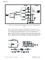
A/D Sample Clock Sources
The PCI-1712/1732 can adopt both internal and external clock sources
for pacer, post-trigger, delay-trigger, about-trigger acquisition modes:
w Internal A/D sample clock with 16-bit Counter
w External A/D sample clock that is connected to AI_CLK on the
PCLD-8712 screw terminal board.
The internal and external A/D sample clocks are described in more
detail as follows.
q Internal A/D Sample Clock
The internal A/D sample clock uses a 10 MHz time base. Conversions
start on the rising edge of the counter output. You can use software to
specify the clock source as internal and the sampling frequency to
pace the operation. The minimum frequency is 152.6 S/s, the maximum
frequency is 2 MS/s. According to the sampling theory (Nyquist
Theorem), you must specify a frequency that is at least twice as fast as
the input’s highest frequency component to achieve a valid sampling.
For example, to accurately sample a 20 kHz signal, you have to specify
a sampling frequency of at least 40 kHz. This consideration can avoid
an error condition often know as aliasing, in which high frequency
input components appear erroneously as lower frequencies when
sampling.
q External A/D Sample Clock
The external A/D sample clock is useful when you want to pace
acquisitions at rates not available with the internal A/D sample clock,
or when you want to pace at uneven intervals. Connect an external A/
D sample clock to screw terminal AI_CLK on the PCLD-8712 screw
terminal board. Conversions will start on the rising edge of the external
A/D sample clock input signal. You can use software to specify the
clock source as external. The sampling frequency is always limited to a
maximum of 2 MHz for the external A/D sample clock input signal.
Advantech Co., Ltd.
www.advantech.com
– 37 –
PCI-1712/1732 User’s Manual
Chapter 5
Figure 5-5: PCI-1712/1732 Sample Clock Source
Trigger Sources
The PCI-1712/1732 supports the following trigger sources for post-,
delay-, about- and pre-trigger acquisition modes:
w Software trigger,
w External digital (TTL) trigger, and
w Analog threshold trigger.
With PCI-1712/1732, user can define the type of trigger source as
rising-edge or falling-edge. These following sections describe these
trigger sources in more detail.
q Software Trigger
A software trigger event occurs when you start the analog input
operation (the computer issues a write to the board to begin acquisitions). When you write the value to analog input trigger flag AI_TRGF
on Write BASE+6 to produce either a rising-edge or falling-edge
trigger, depending upon the trigger source type you choose. This edge
will then act as an A/D trigger event. For detailed information, please
refer to Appendix D.7 A/D Control/Status Register.
q External Digital (TTL) Trigger
For analog input operations, an external digital trigger event occurs
when the PCI-1712/1732 detects either a rising or falling edge on the
External A/D TTL trigger input signal from screw terminal AI_TRG on
PCI-1712/1732 User’s Manual
– 38 –
Advantech Co., Ltd.
www.advantech.com
Chapter 5
the PCLD-8712 screw terminal board. The trigger signal is TTLcompatible.
q Analog Threshold Trigger
For analog input operations, an analog trigger event occurs when the
PCI-1712/1732 detects a transition from above a threshold level to
below a threshold level (falling edge), or a transition from below a
threshold level to above a threshold level (rising edge). User should
connect analog signals from external device or internal analog output
channel on board to external screw terminal ANA_TRG on the PCLD8712 screw terminal board.
On the PCI-1712/1732, the threshold level is set using a dedicated 8-bit
DAC; the hysteresis is fixed at 50 mV. Using software, you can program
the threshold level by writing a voltage value to this DAC; this value
can range from -10 V to +10 V.
Analog Input Data Format
Table 5-2: Analog Input Data Format
A/D code
Mapping Voltage
Hex.
Dec.
Unipolar
Bipolar
000h
0d
0
-FS/2
7FFh
2047d
FS/2 - 1 LSB
-1 LSB
800h
2048d
FS/2
0
FFFh
4095d
FS - 1 LSB
FS/2 - 1 LSB
FS/4096
FS/4096
1 LSB
Table 5-3: The corresponding Full Scale values for various Input
Voltage Ranges
Gain
Uniplar
Bipolar
Range
FS
Range
FS
0.5
N/A
N/A
± 10 V
20
1
0 ~ 10 V
10
±5V
10
2
0~5V
5
± 2.5 V
5
4
0 ~ 2.5 V
2.5
± 1.25 V
2.5
8
0 ~ 1.25 V
1.25
± 0.625 V
1.25
Advantech Co., Ltd.
www.advantech.com
– 39 –
PCI-1712/1732 User’s Manual
Chapter 5
5.2 Analog Output Features
The PCI-1712 card provides two 12-bit multi-range analog output (D/A)
channels. This section describes the following features of the D/A
functions:
w Analog output ranges
w Analog output operation modes
w D/A output clock sources
w Trigger sources
w Analog Output Data Format
Analog Output Ranges
The PCI-1712 provides two 12-bit analog output channels, both of
which can be configured to be applicable within 0 ~ 5 V, 0 ~ 10 V,
± 5 V, ± 10 V output voltage range. On the other hand, users can use
external reference voltage of 0 ~ x V or ± x V output voltage range,
where the value of x is from -10 to +10. Users can configure the output
range during driver installation or in software programming.
Analog Output Operation Modes
The PCI-1712 can output data in single value, continuous output
operation mode. These analog output operation modes are described
in more detail in the following sections:
q Single Value Operation Mode
The single value conversion mode is the simplest way for analog
output operation. Users can define each channel as single output
conversion mode. Then users just need to use software to write output
data to specific I/O register. The analog output channels will output
the corresponding voltage immediately. In the single value operation
mode, users need not set any clock source and trigger source, but only
output voltage range.
q Continuous Output Operation Mode
In continuous output operation mode, users can accurately control the
update rate (up to 1 MS/s with DMA data transferring) between
conversions of individual analog output channels, and takes full
advantage of the PCI-1712. In this mode you can specify a clock
source and trigger source and either of the two analog output channels
to work in continuous output operation mode. But when both of them
operate in this mode, the maximum update rate will be 500 kS/s for each
PCI-1712/1732 User’s Manual
– 40 –
Advantech Co., Ltd.
www.advantech.com
Chapter 5
channel.
In this mode, users need to set the clock source and trigger source
first, and then generate the output data to be stored in the memory
buffers of host PC. The host computer then transfers those data to be
written to the DACs from its buffers to the 32K-sample Output FIFO on
board. When it detects a trigger, the board outputs the values in the
Output FIFO to the DACs at the same time. When the samples in FIFO
decreases to less than half size (i.e. 16K samples) of the FIFO, then the
card will send a interrupt request to the host PC, which in turn sends
16K samples to the FIFO. This output operation will repeat until either
all the data is sent from the buffers or until you stop the operation.
If the two D/A channels are both operating in continuous output
mode, the data in FIFO will be sent in an interlaced manner, i.e. The
“even” samples in the FIFO are sent to D/A channel 0, while the “odd”
samples to D/A channel 1.
q Waveform Output Operation Mode
Waveform output operation mode is a particular and useful application
of continuous output operation mode. In this mode, users can output
the user-defined waveform pattern repetitively and continuously.
Before this operation can begin, users have to use software to allocate
the buffer memory and define the waveform pattern first. Then the host
computer will transfer the waveform pattern from its buffer allocated in
computer memory into the Output FIFO on the board, which in turn will
transfer the waveform pattern to the DACs. When the trigger event
occurs, each D/A channel running continuous output operation mode
will output waveform pattern from FIFO in specific clock rate.
D/A Output Clock Sources
The PCI-1712 can adopt both internal and external clock sources for
pacing the analog output of each channel:
w Internal D/A output clock with 16-bit Counter
w External D/A output clock that is connected to AO_CLK on the
PCLD-8712 screw terminal board
The internal and external D/A output clocks are described in more
detail as follows:
q Internal D/A Output Clock
The internal D/A output clock uses a 10 MHz time base. Conversions
start on the rising edge of the counter output. Through software to
specify the clock source as internal and the clock frequency to pace
Advantech Co., Ltd.
www.advantech.com
– 41 –
PCI-1712/1732 User’s Manual
Chapter 5
the analog output operation. The minimum frequency is 156.2 S/s, the
maximum frequency is 1 MS/s.
q External D/A Output Clock
The external D/A output clock is useful when you want to pace analog
output operations at rates not available with the internal D/A output
clock, or when you want to pace at uneven intervals, or when you
want to start pacing on an external trigger event. Connect an external
D/A output clock to screw terminal AO_CLK on the PCLD-8712 screw
terminal board. Conversions will start on the rising edge of the external
D/A output clock signal. You can use software to specify the clock
source as external. Subsequently, the clock frequency that of the
external D/A output clock input signal from the screw terminal board.
Trigger Sources
The PCI-1712 supports the following trigger sources for continuous
output mode:
w Software trigger,
w External digital (TTL) trigger
With PCI-1712, user can define the type of trigger source as risingedge or falling-edge.
The following section describes these trigger sources in more detail.
q Software Trigger
A software trigger event occurs when you start the analog output
operation (the computer issues a write to the board to begin conversions). When you write the value to analog input trigger flag
AO_TRGF on BASE+A to produce either a rising-edge or falling-edge
trigger, depending upon the trigger source type you choose. This edge
will then act as a D/A trigger event. For detailed information, please
refer to Appendix D.7 A/D Control/Status Register.
q External Digital (TTL) Trigger
For analog output operations, an external digital trigger event occurs
when the PCI-1712 detects either a rising or falling edge on the External
D/A TTL trigger input signal from screw terminal AO_TRG on the
PCLD-8712 screw terminal board. The trigger signal is TTL-compatible.
PCI-1712/1732 User’s Manual
– 42 –
Advantech Co., Ltd.
www.advantech.com
Chapter 5
Analog Output Data Format
Table 5-4: Analog Output Data Format
D/A code
Mapping Voltage
Hex.
Dec.
Unipolar
Bipolar
000h
0d
0
-FS/2
7FFh
2047d
FS/2 - 1 LSB
-1 LSB
800h
2048d
FS/2
0
FFFh
4095d
FS - 1 LSB
FS/2 - 1 LSB
FS/4096
FS/4096
1 LSB
Table 5-5: The corresponding Full Scale values for various Output
Voltage Ranges
Reference
Source
Internal
External
Uniplar
Range
Bipolar
FS
Range
FS
0~5V
5
±5V
10
0 ~ 10 V
10
± 10 V
20
0~xV
x
±xV
2x
5.3 Digital I/O Features
The PCI-1712/1732 supports 16 digital I/O channels. These I/O
channels are divided into two bytes: specifically a low byte, DIO0 to
DIO7; and a high byte, DIO8 to DIO15. You can use each byte as either
an input port or an output port by configuration register; and all eight
channels of the byte have the same configuration. For detailed
information, please refer to Appendix D.16 Digital I/O configuration
registers.
In digital I/O function, you do not need to specify the clock source or
trigger source. When you want to output data, you just need to write
the data to the digital output channel through software. In the same
way, you can use software to read the data from digital input channel.
The default configuration after power on, hardware reset or software
reset is to set all the digital I/O channels to logic-low so that users
need not worry about damaging external devices during system start
up or reset.
Advantech Co., Ltd.
www.advantech.com
– 43 –
PCI-1712/1732 User’s Manual
Chapter 5
5.4 Counter/Timer Features
The PCI-1712/1732 features multifunction counter/timer functions with
one-shot, rate generation, frequency measurement and pulse width
measurement. There are two 8254 counter chips in PCI-1712/1732, and
each chip has 3 multifunction counters. The first counter chip (chip 1)
is specified for AI and AO functions, and can’t be used by user. The
second counter chip (chip 2) is reserved for user, and the following
section describes its features.
The PCI-1712/1732 uses the 82C54 programmable timer/counter chip
includes 3 independent 16-bit down counters: counter 0, counter 1 and
counter 2. Each counter has clock input, gate input and pulse output. It
can be programmed to count from 2 up to 65535.
For detailed information, Intel® 82C54 User’s Manual is available by
accessing the following path on CD-ROM:
\Document\Intel 82C54 manual.pdf
Clock sources
The following clock sources are available for the user counters, and
they are available to set its active edge as rising edge or falling edge:
q Internal clock
User can specify the internal clock as the clock source through
software, and choose among four frequency options: 10MHz, 1MHz,
100kHz and 10kHz of the on-board crystal oscillator. For detailed
information, please refer to Appendix D.14 Counter gate and clock
control/status.
q External clock
The external clock is useful when you want to pace counter/timer
operations at rates not available with the internal clock or if you want
to pace at uneven internals. User can specify an external clock as the
clock source through software. User could connect the external clock
to the PCI-1712/1732 through the PCLD-8712 screw-terminal wiring
board that corresponds to each counter/timer.
q Internally cascaded clock
You can also route the clock output signal from one user counter to the
clock input signal of the next user counter to internally cascade the
counters. In this way, you can create a 32-bit or even a 48-bit counter
without externally cascading multiple counters together. When user
wants to cascade the counters, please follow the round-robin order of
PCI-1712/1732 User’s Manual
– 44 –
Advantech Co., Ltd.
www.advantech.com
Chapter 5
0, 1 and 2. You can choose any counter to be your first cascaded
counter, and the next counter would the next one in the round-robin
order. For example, if you would like to cascade two 16-bit counters
into one 32-bit counter, and you choose counter 1 to be the first
counter then the next counter you choose should be counter 2.
Gate Types and Sources
The gate types and sources you select determine what kind of gate
input signal to enable your counter/timer when receiving clock input. If
the external gate input signal comes in either as logic-low or logic-high
as you have preset, the counter/timer function is enabled, waiting only
for the clock input signal to start counting. The PCI-1712/1732 provides two gate input types, for which user can set easily through
software or write to bit GPn on register Base+20 to 24:
q Logic-low external gate input:
Enables a counter/timer operation when the external gate signal is
logic-low, and disables the counter/timer operation when the external
gate signal is logic-high.
q Logic-high external gate input:
Enables a counter/timer operation when the external gate signal is
logic-high and disables the counter/timer operation when the external
gate signal is logic-low.
The gate sources are described as below:
q Software Gate:
User can use software to generate the signal to be counter’s gate
input. It helps user to control counter easily through software.
q Previous Counter Output:
User can use previous counter’s output as your gate source. The
previous counter of counter 0 is counter 2, of counter 1 is counter 0
and of counter 2 is counter 1.
q External Gate Source:
User can connect an external gate signal to screw terminal
CNTn_GATE on the PCLD-8712 screw terminal board, where n is the
counter number.
Advantech Co., Ltd.
www.advantech.com
– 45 –
PCI-1712/1732 User’s Manual
Chapter 5
Counter/timer operation modes
We enhance the gate function for more applications. For example,
event counting, rate generation, one shot, frequency measurement and
pulse width measurement. We make some innovative arrangements of
clock and gate of counter. For detailed information, please refer to
Appendix D.12 to D.14 and Intel® 82C54 User’s Manual. The following
sections show how to implement counter functions.
q Event counting
The event counting function helps user count events from the
counter’s associated clock input source.
Each counter features 16-bit, and therefore you can count a maximum
of 65,535 events before the counter overflows and returns to 0. If you
need wider range for event counting, you can use a cascaded 32-bit
counter for counting up to 4,294,967,296 events.
Please follow the procedure below when using software:
1. Select a counter ( e.g. counter 0) to do event counting.
2. Set the counter in mode 0 (Please refer to Intel® 82C54 User’s
Manual).
3. Connect the pin CNT0_CLK of the counter to the event signal
source.
4. Set the gate type of the counter to positive (logic-high).
5. Reset the counter to 65,535.
6. Pull high the gate input, and then start down counting.
7. After event counting is finished, read the value from the counter.
8. Calculate the number of events.
For example, if the reset value of counter is 65,535 and the read back
value is 43930, then the number of events is 65535 minus 43930 and
thus equals 21605.
q Rate generation
The rate generation function helps user generate a continuous pulse
output signal from the counter. User can use it as an external clock to
output signal to pace other operations, such as analog input, analog
output, or other counter/timer operations.
The frequency of input clock and the number of the counter determine
the period of the output pulse. If you are using one counter (not
cascaded), you can output pulses with a maximum frequency of 5MHz.
In rate generation mode, either the internal or external clock source is
PCI-1712/1732 User’s Manual
– 46 –
Advantech Co., Ltd.
www.advantech.com
Chapter 5
appropriate depending on your application.
Please follow the procedure below when using software:
1 Select a counter (e.g. counter 0) to do rate generation.
2. Set the counter in mode 3 (Please refer to Intel® 82C54 User’s
Manual).
3. Select the clock input of the counter. (Could be internal or
external)
4. Set the gate type of the counter to positive (logic-high).
5. Set the value of the counter to serve as the factor with which to
divide the clock input frequency.
6. Pull high the gate input and start rate generation.
For example, if the value of counter is 20 and the clock input frequency
is 1 MHz. Then the clock output frequency is 1 MHz / 20 = 50 KHz.
q One shot
Use one-shot mode to generate a single pulse signal from the counter,
which is triggered by the gate input signal.. You can use this pulse
output signal as an external digital (TTL) trigger source to start other
operations, such as analog input or analog output operations. When
the one-shot operation is triggered, only a single pulse is output. The
output pulse is always a negative pulse, whose width is determined by
the clock input signal and the value of the counter.
Please follow the procedure below when using software:
1. Select a counter to do one shot.
2. Set the counter in mode 1 (Please refer to Intel® 82C54 User’s
Manual).
3. Select the clock source of the counter. (Could be internal or
external)
4. Set the gate type of the counter to positive (logic-high).
5. Set the value of the counter to serve as the factor with which to
multiply the clock input period.
6. Pull high the gate input and start to do one-shot output.
For example, if the value of counter is 20 and the frequency of clock
source is 1MHz, the period of the one-shot output source is 20 /
1 MHz = 20 ms.
Advantech Co., Ltd.
www.advantech.com
– 47 –
PCI-1712/1732 User’s Manual
Chapter 5
q Frequency measurement
The frequency measurement function helps user to measure the
frequency of the signal from counter-associated clock input on PCLD8712.
Frequency measurement needs two counters to implement. Use the
first counter to produce a one-shot pulse with defined pulse period to
be the second counter’s gate. Connect the signal source, whose
frequency is to be measured, to the clock input of the second counter.
Since the one-shot pulse generated from the first counter is always a
negative pulse, we have to set the gate input type of the second
counter as logic low for proper frequency measurement.
The second counter starts to count once the gate is set to low and
stops when the gate is high again after a period of time. Assume the
measured frequency signal is the regular pulse, then we can calculate
its frequency by the period of one-shot and the value of second
counter.
Please follow the procedure below when using software:
1. Select the first counter to do one shot and specify its pulse
period.
2. Connect the signal output CNT1_OUT of the first counter to the
second counter’s gate input CNT2_GATE.
3. Select the clock source of the first counter. (Could be internal or
external)
4. Set the gate type of the first counter to positive (logic-high), and
the second counter to negative (logic-low).
5. Reset the second counter to 65,535.
6. Pull high the gate input of the first counter and start to do
frequency measurement.
7. Read the value of the second counter.
8. Evaluate the frequency of the measured pulse.
For example, if frequency measurement is done with the second
counter value set at 65,535 and the period of one-shot from the first
counter set at 0.1 sec, then the value of the second counter we get
back is 43930. Thus, the frequency of measured pulse could be
calculated as (65535-43930)/0.1sec. = 216050 Hz.
PCI-1712/1732 User’s Manual
– 48 –
Advantech Co., Ltd.
www.advantech.com
Chapter 5
Figure 5-6: Frequency measurement
The following C program serves as an example to explain how to
implement the frequency measurement by software.
outport(addr2_1712+0x26,0x03);
while(!kbhit())
{
//Initialize CNT1 and CNT2
outport(addr2_1712+0x24,0x00);
outport(addr2_1712+0x22,0x00);
// Set internal clock as 10 KHz
//Setup CNT1 to output 1 sec. pulse in One-Shot mode
outport(addr2_1712+0x1e,0x72);
//CNT1 82C54 mode 1
outport(addr2_1712+0x1a,0x10);
//Set CNT1 low byte
outport(addr2_1712+0x1a,0x27);
//Set CNT1 high byte
/*CNT1 generate the pulse with 1 sec. period (10KHz/ 10,000 pulse =1
Hz) */
/*Setup CNT2 to count the event of external measured clock signal
during one-shot //pulse from CNT1*/
outport(addr2_1712+0x1e,0xb0);
//CNT2 82C54 mode 0
outport(addr2_1712+0x1c,0xff);
//Set CNT2 low byte
outport(addr2_1712+0x1c,0xff);
//Set CNT2 high byte
Advantech Co., Ltd.
www.advantech.com
– 49 –
PCI-1712/1732 User’s Manual
Chapter 5
//Set the value of CRT2 as 65,535 for down counting
outport(addr2_1712+0x24,0x80);
//Set CNT2’s gate input as high
outport(addr2_1712+0x24,0x88);
outport(addr2_1712+0x24,0x00);
/*Generate one clock to CNT2,
and set CNT2’s gate input as
low*/
outport(addr2_1712+0x24,0x52);
/*Set CNT2’s clock source as
external from CNT1’s OUT, and
negative polarity*/
outport(addr2_1712+0x22,0x80);
outport(addr2_1712+0x22,0x88);
outport(addr2_1712+0x22,0x80);
outport(addr2_1712+0x22,0x81);
//Set CNT1’s gate input as high
//Generate one clock to CNT1
//Set CNT1’s clk source as
//internal
//Check if CNT2’s gate and clock are in logic-high status
//It means that if frequency measurement is in progress
while(i != 0x500)
{
i = inport(addr2_1712+0x24) & 0x0500 ;
}
//The CNT2 has started to do frequency measurement
//Check if CNT2’s gate is in logic-low status
//It checks if frequency measurementis over?
while(1)
{
i = inport(addr2_1712+0x24) & 0x0100 ;
if(i!=0x0100) break;
}
/*The CNT2 has finished the job, and then show the measured
frequency on display*/
dl= inport(addr2_1712+0x1c);
//Read low byte
dh= inport(addr2_1712+0x1c)<<8;
//Read high byte
dh= dh + (dl & 0x00ff);
old_count = 0xffff - dh ;
PCI-1712/1732 User’s Manual
– 50 –
Advantech Co., Ltd.
www.advantech.com
Chapter 5
printf(“Counter 2 = %u \n”,old_count);
old_count = 0;
}
q Pulse width measurement
The pulse width measurement function helps user measure the period
of the signal from counter-associated clock input on PCLD-8712.
Pulse width measurement also needs two counters to implement. Use
the first counter to measure the positive period of the pulse and
second counter to measure the negative period of the pulse (In DLL
driver, it uses CNT1 and CNT2 to implement the pulse width measurement function). To implement the function, we have to connect the
measured pulse signal to the gate of the two counters, and the same
clock source to the clock of the two counters.
Please follow the procedure below when using software:
1. Select the two counters to do event counting.
2. Set both counters in mode 0 (Please refer to Intel® 82C54 User’s
Manual).
3. Connect the measured pulse signal source to pin CNT1_GATE
and CNT2_GATE of both counters
4. Select the clock source of the counter. (Could be internal
external)
5. Connect the clock source to pin CNT1_CLK and CNT2_CLK of
both counters.
6. Set the gate type of the first counter to negative (logic-low).
7. Set the gate type of the second counter to positive (logic-high).
8. Reset both counters to 65,535 and the counters now are ready
for pulse width measurement.
9. On the first incoming pulse, each counter will start measuring
specifically the positive and negative period of the first pulse
cycle.
10.Read the value of both counters.
11.Calculate the width of measured pulse.
For example, if the clock source is of 1KHz, and the reset value of both
counters set to 65,535, then we get a value of 40000 for the first
counter, and 50000 for the second counter. Thus the negative pulse
period is (65535-40000)/1K=25.535 sec, and the positive pulse period is
Advantech Co., Ltd.
www.advantech.com
– 51 –
PCI-1712/1732 User’s Manual
Chapter 5
(65535-50000)/1K = 15.535 sec.
Figure 5-7: Pulse width measurement
The following C program is the example to explain how to implement
the pulse width measurement by software.
outport(addr2_1712+0x26,0x00);
while(!kbhit())
{
outport(addr2_1712+0x1e,0x70);
outport(addr2_1712+0x1a,0xff);
outport(addr2_1712+0x1a,0xff);
//Set internal clock as 10 MHz
outport(addr2_1712+0x1e,0xb0);
outport(addr2_1712+0x1c,0xff);
outport(addr2_1712+0x1c,0xff);
//CNT2 82C54 mode 0
//Set CNT2 low byte
//Set CNT2 high byte
outport(addr2_1712+0x24,0x80);
outport(addr2_1712+0x24,0x88);
outport(addr2_1712+0x24,0x31);
//Set CNT2’s gate input as high
//Generate one clock to CNT2
/*Set CNT2’s clock source as
PCI-1712/1732 User’s Manual
– 52 –
//CNT1 82C54 mode 0
//Set CNT1 low byte
//Set CNT1 high byte
Advantech Co., Ltd.
www.advantech.com
Chapter 5
internal, and gate use for pulse
width measurement*/
outport(addr2_1712+0x22,0x80);
outport(addr2_1712+0x22,0x88);
outport(addr2_1712+0x22,0x71);
//Set CNT1’s gate input as high
//Generate one clock to CNT1
/*Set CNT1’s clock source as
internal, gate use for pulse width
measurement, and negative
polarity*/
/*Reset pulse width measurement state machine, and check if CNT2’s
gate input receives the measured signal*/
while(1)
{
outport(addr2_1712+0x24,0x0031); //Generate a rising edge to
//reset the pulse
outport(addr2_1712+0x24,0x0131); //width measurement state
//machine
i = inport(addr2_1712+0x24) & 0x0800;
/*Check if receiving
measured signal
from gate input of
CNT2*/
if (i == 0x0800) break ;
}
outport(addr2_1712+0x22,0x0071); //Generate a rising edge to reset
//the pulse
outport(addr2_1712+0x22,0x0171); //width measurement state
//machine
//CNT2’s gate input receiving the measured signal, check if finished
while(1)
{
i = inport(addr2_1712+0x24) & 0x0800;
if(i == 0x0000) break;
//CNT2’s gate input is low
}
Advantech Co., Ltd.
www.advantech.com
– 53 –
PCI-1712/1732 User’s Manual
Chapter 5
//CNT1’s gate input received the measured signal, check if finished?
while(1)
{
i = inport(addr2_1712+0x22) & 0x0800;
if(i == 0x0000) break;
//CNT1’s gate input is low
}
/*The CNT1 & 2 has finished the job, and then show the measured
period on display*/
dl= inport(addr2_1712+0x1a);
//Read low byte
dh= inport(addr2_1712+0x1a)<<8; //Read high byte
dh= dh + (dl & 0x00ff);
neg_count = 0xffff - dh ;
dl= inport(addr2_1712+0x1c);
dh= inport(addr2_1712+0x1c)<<8;
dh= dh + (dl & 0x00ff);
pos_count = 0xffff - dh ;
duty = pos_count;
duty = duty + neg_count;
duty = (pos_count/duty)*100;
//Show the duty ratio of positive
cycle
printf(“P+ = %u P- = %u Duty %5.3f \n”,pos_count,neg_count,
duty);
neg_count = 0;
pos_count = 0;
}
PCI-1712/1732 User’s Manual
– 54 –
Advantech Co., Ltd.
www.advantech.com
6
Chapter 6
Chapter
6. Calibration
This chapter provides brief information on PCI-1712/1732 calibration.
Regular calibration checks are important to maintain accuracy in data
acquisition and control applications. A calibration utility, AutoCali, is
included on the companion CD-ROM :
AutoCali.EXE
PCI-1712/1732 calibration utility
This calibration utility is designed for the Microsoft©Windows™
environment. Access this program from the default location:
C:\Program Files\Advantech\ADSAPI\Utility\PCI1712
Note:
✎ If you installed the program to another directory, you can find these
programs in the corresponding subfolders in your destination directory.
The PCI-1712/1732 has been calibrated at the factory for initial use.
However, a calibration of the analog input and the analog output
function every six months is recommended.
6.1 VR Assignment
There is one variable resistor (VR1) on the PCI-1712/1732 to adjust the
accurate reference voltage on the PCI-1712/1732. We have provided a
test point (See TP5 in Figure 6-1) for you to check the reference
voltage on board. You will need a precise 4½-digit digital multi-meter.
Before you start to calibrate A/D and D/A channels, please adjust VR1
until the reference voltage on TP5 has reached +5.0000 V. Figure 6-1
shows the locations of VR1 and TP5.
Figure 6-1: PCI-1712/1732 VR1 & TP5
Advantech Co., Ltd.
www.advantech.com
– 55 –
PCI-1712 User’s Manual
Chapter 6
6.2 A/D Calibration
Regular and proper calibration procedures ensure the maximum
possible accuracy. It is easy to complete the A/D calibration procedure automatically (i.e. through software calibration) by executing the
A/D calibration program AutoCali. Therefore, it is not necessary to
adjust the hardware settings of the PCI-1712/1732. However, the
following calibration steps are also provided for your reference in case
manual calibration is needed:
1. Adjust VR1 until the reference voltage on TP5 has reached
+5.0000 V.
2. Set PCI-1712 to calibration mode, which will configure AI2 to +5
V, and AI0 to 0 V. (Write “1” in AI0_CAL at the register address
BASE+6 bif7).
3. Adjust the PGA offset voltage. First, set the analog input voltage
range of AI0 to ±10V. Adjust the PGA offset register (BASE+2C),
and acquire a value from AI0 in single value acquisition mode.
Then switch the analog voltage range to ±1.25V to repeat the
operation in this step again to acquire a value from AI0. Repeat
this cycle several times. Meanwhile, adjust the PGA offset
voltage until the AI0’s values become the same for both the
analog input range ±10 V and ±1.25 V.
4. Adjust the gain value of the PGA. First, set the analog input
voltage range of AI2 between 0 and 5V. Adjust the gain register
(Base+2C), and then acquire the value for AI2 from single value
acquisition mode. Adjust the gain value of the PGA until the
subsequent AI2’s values converge within the Ox0ffe to
Ox0fff range.
5. Adjust the bipolar offset voltage. First, set the analog input
range within ±2.5 V. Adjust the bipolar offset register (Base+2C),
and then acquire the code from AI0 from single value acquisition
mode. Adjust the bipolar offset voltage until the AI0’s code
flickers around Ox0800.
6. Adjust unipolar offset voltage. First, set the analog input range
within 0 and 5 V. Adjust the unipolar offset register (Base+2C),
and then acquire the code for AI0 from single value acquisition
PCI-1712/1732 User’s Manual
– 56 –
Advantech Co., Ltd.
www.advantech.com
Chapter 6
mode. Adjust the gain until the AI0’s value converges between 0
and 1.
7. Repeat steps 4 to 6 several times.
6.3 D/A Calibration
You can select an on-board +5V or +10V internal reference voltage or
an external voltage as your analog output reference voltage. If you
use an external reference, connect the reference voltage within the
±10V range to the reference input of the D/A output channel you want
to calibrate. Then adjust the gain value, unipolar offset voltage, bipolar
offset voltage, respectively, of D/A channels 0 and 1 with the associated register (BASE+2C).
Note:
✎ A precision voltmeter is recommended to calibrate the D/A outputs.
The auto-calibration program AutoCali.EXE helps you finish the D/A
calibration procedure automatically. In order to get the maximum
possible accuracy of the D/A channels, you need to calibrate the A/D
channels first. Although the procedure is not necessary, the following
calibration steps are provided below for your reference in case you
want to implement the calibration yourself:
1. Calibrate the A/D channels first.
2. Set PCI-1712 in calibration mode. AI4 is connected to AO0 and
AI6 is connected to AO1. (Write “1” to the bit, AIO_CAL, on
register BASE+6 bit7)
3. Set the unipolar output range of both AO0 and AO1 the same as
the internal or external reference voltage range, either 0 to 5V or
0 to 10 V.
4. Set the output value of the AOn (where n=0 or 1) data register at
(BASE+0x0C) as 0x0ffe and output to AOn.
5. Adjust the associated gain register (BASE+0x0C) until the AOn
output value reads AI4+2n equals 0x0ffe.
6. Set the output value of the AOn data register (BASE+0x0C) as
0x0001 and output to AOn.
7. Adjust the associated unipolar offset register (BASE+0x2C) until
Advantech Co., Ltd.
www.advantech.com
– 57 –
PCI-1712/1732 User’s Manual
Chapter 6
the AOn output code reads AI4+2n equals 0x0001.
8. Set the bipolar output range of AO0 and AO1 the same as the
reference voltage within -10 to +10 V.
9. Set the output value of AOn data register (BASE+0x0C) as
0x0800 and output to AOn.
10.Adjust teh associated bipolar offset register (BASE+0x2C) until
the AOn output code reads AI4+2n equals 0x0800.
11.Repeat steps 3 to 10 several times.
6.4 Calibration Utility
The calibration utility,AutoCali, provides four functions - auto A/D
calibration, auto D/A calibration, manual A/D calibration and manual D/
A calibration. The program helps the user to easily finish the calibration procedures automatically; however, the user can calibrate the PCI1712/1732 manually. Sections 6.2 and 6.3 illustrated the standard
calibration procedures for your reference. If you want to calibrate the
hardware in your own way, these two sections will guide you.
The following steps will guide you through the PCI-1712/1732 software
calibration.
Step 1: Access the calibration utility program AutoCali.exe from the
default location:
C:\Program Files\Advantech\ADSAPI\Utility\PCI1712
Note:
✎ If you installed the program to another directory, you can find this
program in the corresponding subfolders in your destination directory.
Step 2: Select PCI-1712/1732 in the ADSDAQ dialog box.
Figure 6-2: Selecting the device you want to calibrate
PCI-1712/1732 User’s Manual
– 58 –
Advantech Co., Ltd.
www.advantech.com
Chapter 6
Step 3: After you start to calibrate the PCI-1712/1732, please don’t
forget to adjust VR1.
Figure 6-3: Warning message before start calibration
A/D channel Auto-Calibration
Step 4: Click the Auto A/D Calibration tab to show the A/D channel
auto-calibration panel (Fig. 6-4). Press the start button to
calibrate A/D channels automatically.
Figure 6-4: Auto A/D Calibration Dialog Box
Advantech Co., Ltd.
www.advantech.com
– 59 –
PCI-1712/1732 User’s Manual
Chapter 6
Step 5: The first A/D calibration procedure is enabled (Fig. 6-5).
Figure 6-5: A/D Calibration Procedure 1
Step 6: The second A/D calibration procedure is enabled (Fig. 6-6)
Figure 6-6: A/D Calibration Procedure 2
PCI-1712/1732 User’s Manual
– 60 –
Advantech Co., Ltd.
www.advantech.com
Chapter 6
Step 7: The third A/D calibration procedure is enabled (Fig. 6-7)
Figure 6-7: A/D Calibration Procedure 3
Step 8: Auto-calibration is finished. (See fig. 6-8)
Figure 6-8: A/D Calibration is finished
Advantech Co., Ltd.
www.advantech.com
– 61 –
PCI-1712/1732 User’s Manual
Chapter 6
D/A channel Auto-Calibration
Step 9: Click the Auto D/A Calibration tab to show the D/A channel
auto calibration panel. Please finish the A/D calibration
procedure first before you start the D/A calibration procedure.
There are two D/A channels in PCI-1712; select the output
range for each channel and then press the start button to
calibrate D/A channels (Fig. 6-9).
Figure 6-9: Range Selection in D/A Calibration
Step 10: D/A channel 0 calibration is enabled (Fig. 6-10)
Figure 6-10: Calibrating D/A Channel 0
PCI-1712/1732 User’s Manual
– 62 –
Advantech Co., Ltd.
www.advantech.com
Chapter 6
Step 11: D/A channel 1 calibration is enabled (Fig. 6-11)
Figure 6-11: Calibrating D/A Channel 1
Step 12: Auto-calibration is finished (Fig. 6-12)
Figure 6-12: D/A Calibration is finished
Advantech Co., Ltd.
www.advantech.com
– 63 –
PCI-1712/1732 User’s Manual
Chapter 6
A/D channel Manual-Calibration
Step 1: Click the Manual A/D Calibration tab to show the A/D
channel manual calibration panel. Before calibrating, acquire
the reference voltage from a precision standard voltage
reference. Go to the Range form, select a channel and the
target voltage range according to the input voltage value from
a precision standard voltage reference(Fig. 6-13).
Note:
✎ The input voltage value you selected from a precision standard
voltage reference needs to correspond with the one that the
PCI-1712/1732 can read.
✎ The input voltage will be analog code so the computer will
convert the voltage data into digitial code; therefore, the input
voltage value you selected from a precision standard voltage
reference needs to correspond with the one that the PCI-1712/1732
can read. For example, if the input range is 0 ~ 5V, then input
voltage should be 2.9992V not 3V.
Figure 6-13: Selecting Input Rage in Manual A/D Calibration panel
PCI-1712/1732 User’s Manual
– 64 –
Advantech Co., Ltd.
www.advantech.com
Chapter 6
Step 2: According to the difference between reference voltage and
receiving data in PCI-1712/1732, adjust the gain, bipolar offset
and unipolar offset registers (Figure 6-14)
Figure 6-14: Adjusting registers
Step 3: Adjust the registers until they fall between the input voltage
from the standard voltage reference and the receiving voltage
reflectected in the Manual A/D Calibration tab.
Advantech Co., Ltd.
www.advantech.com
– 65 –
PCI-1712/1732 User’s Manual
Chapter 6
D/A channel Manual-Calibration
Step 1: Click the Manual D/A Calibration tab to show the D/A
channel manual calibration panel. Two D/A channels are
individually calibrated . Before calibrating, output desired
voltage from the D/A channels and measure it through an
external precision multimeter.
Step 2: For example, choose channel 0; select the Range and select the
wished output voltage code or value from the radio buttons
(Fig. 6-15 and Fig. 6-16).
Figure 6-15 & Figure 6-16: Selecting D/A Range and
Choosing Output Voltage
PCI-1712/1732 User’s Manual
– 66 –
Advantech Co., Ltd.
www.advantech.com
Chapter 6
Step 3: According to the difference between the output voltage from
D/A channel and the value in the multimeter, adjust the gain,
bipolar offset and unipolar offset registers (Fig. 6-17)
Figure 6-17: Adjusting registers
Step 4: Adjust registers until they fall between the output voltage from
the D/A channel and the value in the multimeter.
Advantech Co., Ltd.
www.advantech.com
– 67 –
PCI-1712/1732 User’s Manual
Chapter 6
PCI-1712/1732 User’s Manual
– 68 –
Advantech Co., Ltd.
www.advantech.com
A
Chapter 4
Appendix
A. Specification
Analog Input:
Channels
16 single-ended or 8 differential or combination
Resolution
12-bit
FIFO Size
1K samples
Max. Transfer Rate
Conversion Time
Input range and
Gain List
Drift
Small Signal Bandwidth for
PGA
Common mode voltage
Max. Input voltage
Input Protect
Input Impedance
Trigger Mode
Multi-channel, single gain: 1 MS/s
Multi-channel, multi-gain: 600 kS/s
Multi-channel, multi-gain, unipolar/bipolar: 400 kS/s
500 ns
Gain
0.5
1
2
4
8
Unipolar
N/A
0~10
0~5
0~2.5
0~1.25
Bipolar
± 10
±5
± 2.5
± 1.25
± 0.625
Gain
0.5
1
2
4
8
Zero(µV/° C)
± 80
± 30
± 30
± 30
± 30
Gain(ppm/° C)
± 30
± 30
± 30
± 30
± 30
Gain
0.5
1
2
4
8
Bandwidth
4.0 MHz
4.0 MHz
2.0 MHz
1.5 MHz
0.65 MHz
± 11 V max. (operational)
± 20 V
30 Vp-p
100 MΩ/10pF(Off); 100 MΩ/100pF(On)
Software, on-board programmable pacer or external, pre-trigger, post-trigger,
delay-trigger, about-trigger
DNLE:± 1LSB
INLE: ± 1LSB
DC Offset error < 1LSB
Accuracy
Gain
0.5
1
2
4
8
Gain error
(% FSR)
0.15
0.03
0.03
0.05
0.1
SNR: 68 dB
AC ENOB: 11 bits
THD: -75 dB typical
External TTL Trigger Input
Low
0.8 V max.
High
2.0 V min.
Range
External Analog
Trigger Input
Clock Output
Trigger Output
Advantech Co., Ltd.
www.advantech.com
-10 V to + 10 V
Resolution
8-bit
Impedance
100 MΩ/100 pF typical
Low
0.5 V max.@+24 mA
High
2.4 V min.@-15 mA
Low
0.5 V max.@+24 mA
High
2.4 V min.@-15 mA
– 69 –
PCI-1712 User’s Manual
APPENDIX A
Analog Output: (PCI-1712 only)
Channels
2
Resolution
12-bit
FIFO Size
32K samples
Operation mode
Output Range (Internal
& External Reference)
Accuracy
Single output, continuous output, waveform output
Using Internal Reference
0~+5V,0~+10 V, -5~+5V,-10~+10V
Using External Reference
0 ~ +x V@ +x V (-10 ≤ x ≤ 10
-x ~ +x V@ +x V (-10 ≤ x ≤ 10)
Relative
± 1 LSB
Differential Non-linearity
± 1 LSB (monotonic)
Offset
< 1 LSB
Slew Rate
20V/µs
Drift
Driving Capability
10 ppm/° C
± 10mA
Max. Transfer Rate
Single Channel: 1 MS/s max. for FSR
Dual Channel: 500 kS/s max. for FSR
Output Impedance
0.1Ω max.
Digital Rate
5 MHz
Settling Time
2µs(to ±1/2 LSB of FSR)
External Clock Input
External TTL Trigger
Input
Low
0.8 V max.
High
2.0 V min.
Low
0.8 V max.
High
2.0 V min.
Digital Input /Output:
Input Channels
16 (bi-directional)
Number of ports
2
Input Voltage
Output Voltage
Low
0.8 V max.
High
2.0 V min.
Low
0.5 V max.@+24 mA (sink)
High
2.4 V min.@-15 mA (source)
PCI-1712/1732 User’s Manual
– 70 –
Advantech Co., Ltd.
www.advantech.com
APPENDIX A
Counter/Timer:
Channels
Resolution
Compatibility
Base Clock
Max. Input Frequency
Clock Input
Gate Input
Counter Output
3
16-bit
TTL level
10 MHz, 1MHz, 100kHz, 10kHz
10 MHz
Low
0.8 V max.
High
2.0 V min.
Low
0.8 V max.
High
2.0 V min.
Low
0.5 V max.@+24 mA
High
2.4 V min.@-15 mA
General:
I/O Connector Type
Dimensions
Power Consumption
Temperature
68-pin SCSI-II female
175 mm x 100 mm (6.9" x 3.9")
Typical
+5 V @ 850 mA +12 V @ 600 mA
Max.
+5 V @ 1 A +12 V @ 700m A
Operation
0~+60° C (32~140° F)
(refer to IEC 68-2-1,2)
Storage
-20~+85° C (-4~185° F)
Relative Humidity
5~95%RH non-condensing (refer to IEC 68-2-3)
Certification
CE certified
Note:
✎ The sampling rate depends on the computer hardware architecture and
software environment. The rates may vary due to programming
language, code efficiency, CPU utilization and so on.
Advantech Co., Ltd.
www.advantech.com
– 71 –
PCI-1712/1732 User’s Manual
APPENDIX A
PCI-1712/1732 User’s Manual
– 72 –
Advantech Co., Ltd.
www.advantech.com
B
APPENDIX B
Appendix
B. Block Diagram
Block Diagram
PCI BUS
8 b it D /A
C L K [3 :0 ]
G AT E [ 3 : 0 ]
40MHz
OSC.
PCI9054
PCI Interface
A I_T R G
Trigger and
Control Logic
_
A n a lo g T r i g g e r
C om pare
3 User
16bit
Timer/
Counter
AO _TRG
+
AN A_TR G
D IO [7 :0 ]
Bidierctional
and Latched
8 bit DIO
LOCAL BUS
O U T [3 :0 ]
1K
FIFO
+
1 2 b it A /D
P G IA
_
16 S/E
or
8 DIFF
MUX
A I[1 5 :0 ]
A I_C L K
D I O [ 1 5 :8 ]
Bidierctional
and Latched
8 bit DIO
32K
FIFO
2 Channel
1 2 b it D /A
A O [1 :0 ]
AO _CLK
Advantech Co., Ltd.
www.advantech.com
– 73 –
PCI-1712/1732 User’s Manual
APPENDIX B
PCI-1712/1732 User’s Manual
– 74 –
Advantech Co., Ltd.
www.advantech.com
C
APPENDIX C
C. Screw-terminal Board
Appendix
C. 1 Introduction
The PCLD-8712 Screw-terminal Board provides convenient and reliable
signal wiring for the PCI-1712/1732 of which has a 68-pin SCSI-II
connector. Due to its special PCB layout you can install passive
components to construct your own signal-conditioning circuits. The
user can easily construct a low-pass filter, attenuator or current shunt
converter by adding resistors and capacitors on board’s circuit pads.
C. 2 Features
• Low-cost screw-terminal board for the PCI-1712/1732 with 68-pin
SCSI-II connector.
• Reserved space for signal-conditioning circuits such as low-pass
filter, voltage attenuator and current shunt.
• Industrial-grade screw-clamp terminal blocks for heavy-duty and
reliable connections.
• DIN-rail mounting case for easy mounting.
• Dimensions:169 mm (W) x 112mm (L) x 51mm (H) (6.7" x 4.4" x 2.0")
C. 3 Board Layout
Figure C-1: PCLD-8712 board layout
Advantech Co., Ltd.
www.advantech.com
– 75 –
PCI-1712/1732 User’s Manual
APPENDIX C
CN1: 68-pin SCSI-II connector for connection with the PCI-1712
CN2: 20-pin connector for digital I/O
C.4 Pin Assignment
CN2
DIO 0
1
2
DIO 1
DIO 2
3
4
DIO 3
DIO 4
5
6
DIO 5
DIO 6
7
8
DIO 7
DIO 8
9
10
DIO 9
DIO 10
11
12
DIO 11
DIO 12
13
14
DIO 13
DIO 14
15
16
DIO 15
DGND
17
18
DGND
+5 V
19
20
+12 V
Figure C-2: CN2 pin assignments for the PCLD-8712
PCI-1712/1732 User’s Manual
– 76 –
Advantech Co., Ltd.
www.advantech.com
APPENDIX C
C.5 Single-ended Connections
a) Straight-through connection
(factory setting)
RAn = 0 Ω (short)
RBn = none
Cn = none
b) 1.6 kHz (3dB) low pass filter
RAn = 10 k Ω
RBn = none
Cn = 0.01 µF
1
f3dB = 2πKRAnCn
c) 10 : 1 voltage attenuator:
RAn = 9 k Ω
RBn = 1 k Ω
Cn = none
Attenuation = RAnRBn
+ RBn
d) 4 ~ 20 mA to 1 ~ 5 VDC signal
converter:
RAn = 0 Ω (short)
RBn = 250 Ω (0.1% precision
resistor)
Cn = none
Advantech Co., Ltd.
www.advantech.com
– 77 –
PCI-1712/1732 User’s Manual
APPENDIX C
C.6 Differential Connections
a) Straight-through connection (factory
setting):
RAn = 0 Ω (short)
RAn+1 = 0 Ω (short)
RDn = none
CDn = none
b) 1.6 kHz (3dB) low pass filter
RAn = 5 kΩ
RAn+1 = 5 kΩ
RDn = none
CDn = 0.01 µF
1
f3dB = 2π (RAn+RAn+1) CDn
c) 10 : 1 voltage attenuator:
RAn = 4.5 k Ω
RAn+1 = 4.5 kΩ
RDn = 1 kΩ
Cn = none
RDn
Attenuation = RAn+RAn+1+RDn
d) 4 ~ 20 mA to 1 ~ 5 VDC signal
converter:
RAn = 0 Ω (short)
RAn+1 = 0 Ω (short)
RDn = 250 Ω (0.1% precision resistor)
CDn = none
3. Calculations
PCI-1712/1732 User’s Manual
– 78 –
Advantech Co., Ltd.
www.advantech.com
D
APPENDIX D
Appendix
D. Register Structure and Format
D.1 Overview
The PCI-1712/1732 is delivered with an easy-to-use 32-bit DLL driver
for user programming under Windows 95/98/NT operating system. We
dvise users to program the PCI-1712/1732 using 32-bit DLL driver
provided by Advantech to avoid the complexity of low-level programming by register.
The most important consideration in programming the PCI-1712/1732 at
the register level is to understand the function of the card’s registers.
The information in the following sections is provided for users who
would like to do their own register-level programming.
D.2 I/O Port Address Map
The PCI-1712/1732 requires 50 consecutive addresses in the PC’s I/O
space. The address of each register is specified as an offset from the
card’s base address. For example, BASE+0 is the card’s base address
and BASE+8 is the base address plus eight bytes. The following
sections give the detailed information about register layout, and also
the detailed information about each register or driver and its address
relative to the card’s base address.
Table D-1 shows the function of each register or driver and its address
relative to the card’s base address.
Note
✎ All base address is in hexadecimal in Appendix D.
✎ Users have to use a 16-bit (word) I/O command to read/write each
register.
Advantech Co., Ltd.
www.advantech.com
– 79 –
PCI-1712 User’s Manual
APPENDIX D
Table D-1: PCI-1712/1732 register format (Part 1)
Base
Address
PCI-1712/1732 Register Format
15
14
13
12
11
10
9
8
7
6
5
4
3
2
1
0
A/D single value acquisition
W
0
Channel and A/D data
R
AF
CH2
CH1 CH0 AD11 AD10 AD9 AD8 AD7 AD6 AD5 AD4
AD3 AD2
AD1 AD0
A/D channel range setting
W
S/D B/U
G2
G1
G0
2
N/A
R
Multiplexer setting
W
STP3 STP2 STP1 STP0
STR3 STR2 STR1 STR0
4
N/A
R
A/D control register
W
6
AI_ DMA
TRGF _TCF
AIO_
CAL
AD_
AD_
TRE
TR
AD_
ADM2 ADM1 ADM0
CLK
AD_
TR
AD_
ADM2 ADM1 ADM0
CLK
A/D status register
R
AI_ DMA
TRGF _TCF
AD_
TRE
Clear interrupt and FIFO
W
8
CLR
_DAF
CLR
_ADF
Clear interrupt
Interrupt and FIFO status
R
D/A_ D/A_ D/A_
F/F
F/H
F/E
A/D_ A/D_ A/D_
F/F
F/H
F/E
INT_
F
D/A control register
W
AO_
TRGF
DA_
CLK
A
DAM- DAM1
0
DA1
_U/B
DA1
_I/E
DA1
_5/10
DA_
U/B
DA0
_I/E
DA0
_5/10
DA1
_I/E
DA1
_5/10
DA_
U/B
DA0
_I/E
DA0
_5/10
DA5
DA4
DA3
DA2
DA1
DA0
DA5
DA4
DA3
DA2
DA1
DA0
D/A status register
R
AO_
TRGF
DA_
CLK
DA1
_U/B
DAM1 DAM0
D/A channel 0 data
W
DA11 DA10
DA9
DA8
DA7
DA6
C
N/A
R
D/A channel 1 data
W
DA11 DA10
DA9
DA8
DA7
DA6
E
N/A
R
PCI-1712/1732 User’s Manual
– 80 –
Advantech Co., Ltd.
www.advantech.com
APPENDIX D
Table D-1: PCI-1712/1732 register format (Part 2)
Base
Address
PCI-1712/1732 Register Format
15
14
13
12
11
10
9
8
7
6
5
4
3
2
1
0
D6
D5
D4
D3
D2
D1
D0
D6
D5
D4
D3
D2
D1
D0
D6
D5
D4
D3
D2
D1
D0
D6
D5
D4
D3
D2
D1
D0
D5
D4
D3
D2
D1
D0
D6
D5
D4
D3
D2
D1
D0
D6
D5
D4
D3
D2
D1
D0
D6
D5
D4
D3
D2
D1
D0
D6
D5
D4
D3
D2
D1
D0
D6
D5
D4
D3
D2
D1
D0
D6
D5
D4
D3
D2
D1
D0
D6
D5
D4
D3
D2
D1
D0
D6
D5
D4
D3
D2
D1
D0
D6
D5
D4
D3
D2
D1
D0
D6
D5
D4
D3
D2
D1
D0
D6
D5
D4
D3
D2
D1
D0
D/A counter 0
W
D7
10
D/A counter 0
R
D7
A/D counter 1
W
D7
12
A/D counter 1
R
D7
DMA counter 2
W
D7
D6
14
DMA counter 2
R
D7
Counter control
W
D7
16
Counter control
R
D7
Counter 0
W
D7
18
Counter 0
R
D7
Counter 1
W
D7
1A
Counter 1
R
D7
Counter 2
W
D7
1C
Counter 2
R
D7
Counter control
W
D7
1E
Counter control
R
D7
Advantech Co., Ltd.
www.advantech.com
– 81 –
PCI-1712/1732 User’s Manual
APPENDIX D
Table D-1: PCI-1712/1732 register format (Part 3)
Base
Address
PCI-1712/1732 Register Format
15
14
13
12
11
10
9
8
7
6
5
4
3
2
1
0
G00
CQ0
CP0
C01
C00
G00
CQ0
CP0
C01
C00
G10
CQ1
CP1
C11
C10
G10
CQ1
CP1
C11
C10
G20
CQ2
CP2
C21
C20
G20
CQ2
CP2
C21
C20
Counter 0 gate and clock control
W
GR0
20
GQ0
GP0
G01
Counter 0 gate and clock status
R
GATE
GATCLK0 OUT0
S0
E0
GQ0
GP0
G01
Counter 1 gate and clock control
W
GR1
22
GQ1
GP1
G11
Counter 1 gate and clock status
R
GATGATCLK1 OUT1
ES1
E1
GQ1
GP1
G11
Counter 2 gate and clock control
W
GR2
24
GQ2
GP2
G21
Counter 2 gate and clock status
R
GATGATCLK2 OUT2
ES2
E2
GQ2
GP2
G21
Counter internal clock source select register
W
CLK_- CLK_SEL1 SEL0
26
N/A
R
Digital Output
W
DO15 DO14 DO13 DO12 DO11 DO10
DO9
DO8
DO7
DO6
DO5
DO4
DO3
DO2
DO1
DO0
DI6
DI5
DI4
DI3
DI2
DI1
DI0
28
Digital Input
R
DI15
DI14
DI13
DI12
DI11
DI10
DI9
DI8
DI7
Digital I/O configuration register
W
2A
DIO_C1
DIO_C0
DIO_C1
DIO_C0
Digital I/O configuration register
R
Calibration command and data
W
CM3
CM2
CM1
CM0
D7
D6
D5
D4
D3
D2
D1
D0
DA2
DA1
DA0
2C
N/A
R
N/A
W
2E
N/A
R
D/A channel data for continuous output operation mode
30
W
DA11 DA10
PCI-1712/1732 User’s Manual
DA9
DA8
– 82 –
DA7
DA6
DA5
DA4
DA3
Advantech Co., Ltd.
www.advantech.com
APPENDIX D
D.3 A/D Single Value Acquisition Write BASE+0
The A/D converter will convert one sample when you write to the
register Write BASE+0 with any value. User can check the A/D FIFO
status (A/D_F/E on register Read BASE+8) to make sure if the data is
ready to be received.
D.4 Channel and A/D data Read BASE + 0
These two bytes in Read BASE+0 hold the result of A/D conversion
data.
The 12 bits of data from the A/D conversion are stored in bit 0 to bit
11, bit 12 to 14 hold the A/D channel number and bit 15 holds the
trigger event flag.
Table D-2: Register for channel number and A/D data
Base Add.
15
14
13
12
11
10
9
8
7
6
5
4
3
2
1
0
AD5
AD4
AD3
AD2
AD1
AD0
Channel and A/D data
0
R
AF
CH2
CH1
CH0
AD11 AD10 AD9
AD8
AD7
AD6
AD11 TO AD0
Data of A/D Conversion
AD0
the least significant bit (LSB) of A/D data.
AD11
the most significant bit (MSB) of A/D data.
CH2 to CH0
A/D Channel Number
CH2 ~ CH0 hold the A/D channel number from which the data is
received.
CH2
MSB.
CH0
LSB.
Note:
✎ A/D channel number specifies the channel from which data is derived.
CH2 is the MSB and CH0 is the LSB. For channel scan, there should
have 4 channel codes, specifically from CH0 to CH3. Because we have
not enough address space, bit 15 is used for other purposes instead for
CH3, which is hence not available..
AF A/D trigger event flag
The trigger flag indicates whether a trigger event has happened during
A/D conversion process.
Advantech Co., Ltd.
www.advantech.com
– 83 –
PCI-1712/1732 User’s Manual
APPENDIX D
0 means the data on AD11 to AD0 is stored before trigger.
1 means the data on AD11 to AD0 is stored after trigger.
The trigger event flag plays an important role in post-, delay-, aboutand pre-trigger acquisition modes. For detailed information, please
refer to Chapter 5.1 Analog Input Features.
D.5 A/D Channel Range Setting Write BASE+2
Each A/D channel has its own input range, controlled by a gain code
stored in on-board RAM.
To change the A/D channel input range for a channel:
w Write the same channel in Write BASE+4 bit 0 to bit 3 (the start
channel) and bit 8 to bit 11 (the stop channel).
w Write the gain code to Write BASE+2 bit 0 to bit2.
w Write 0 or 1 to Write BASE+2 bit 4 to set unipolar or bipolar input.
Table D-3: Register for A/D channel range setting
Base Add.
15
14
13
12
11
10
9
8
7
6
5
4
3
S/D
B/U
2
1
0
G2
G1
G0
A/D channel range setting
2
W
S/D
Single-ended or Differential
0 means the channel is single-ended input.
1 means the channel is differential input.
B/U
Bipolar or Unipolar
0 means the channel is bipolar.
1 means the channel is unipolar.
G2 to G0
Gain Code
PCI-1712/1732 User’s Manual
– 84 –
Advantech Co., Ltd.
www.advantech.com
APPENDIX D
Table D-4: Gain Codes for the PCI-1712/1732
Gain Code
B/U
Gain
Input Range (V)
G2
G1
G0
0
0
0
0
1
-5 ~ +5
0
0
0
1
2
-2.5 ~ +2.5
0
0
1
0
4
-1.25 ~ +1.25
0
0
1
1
8
-0.625 ~ +0.625
0
1
0
0
0.5
-10 ~ +10
1
0
0
0
1
0 ~ 10
1
0
0
1
2
0~5
1
0
1
0
4
0 ~ 2.5
1
0
1
1
8
0 ~ 1.25
D.6 MUX Control Write BASE+4
Table D-5: Register for multiplexer control
Base Add.
15
14
13
12
11
10
9
8
7
6
5
4
3
2
1
0
Multiplexer setting
4
W
STP3 STP2 STP1 STP0
STR3 STR2 STR1 STR0
STR3 ~ STR0
Start Scan Channel Number
STP3 ~ STP0
Stop Scan Channel Number
When you set the gain code of analog input channel n, you should set
the MUX start & stop channel number to channel n to prevent any
unexpected errors. In fact, Write BASE+4 bit 3 to 0, STR3 ~ STR0, act
as a pointer to the address of channel n in the SRAM when you
program the A/D channel setting (refer to Section D.5).
Note:
✎ We recommend that you set the same start and stop channel when
writing to the register Write BASE+2. Otherwise, if the A/D trigger
source is on, the multiplexer will continuously scan between channels
and the range settings may be set to an unexpected channel. Make sure
the A/D trigger source is turned off to avoid this kind of error.
Advantech Co., Ltd.
www.advantech.com
– 85 –
PCI-1712/1732 User’s Manual
APPENDIX D
The write-only register of Write BASE+4 controls how the multiplexers
(MUXs) scan.
w Write BASE+4 bit 3 to bit 0, STR3 ~ STR0, hold the start scan
channel number.
w Write BASE+4 bit 11 to bit 8, STP3 ~ STP0, hold the stop scan
channel number.
Writing to the register automatically initializes the MUXs to the start
and stop channel. Each A/D conversion trigger also sets MUXs to the
next channel. With continuous triggering, the MUXs will scan from the
start channel to the stop channel and then repeat. The following
examples show the scan sequences of the MUXs (all channels are set
as single-ended).
Example 1
If the start scan input channel is AI3 and the stop scan input channel
is AI7, then the scan sequence is AI3, AI 4, AI 5, AI6, AI7, AI3, AI4,
AI5, AI6, AI7, AI3, AI4...
Example 2
If the start scan input channel is AI13 and the stop scan input channel
is AI2, then the scan sequence is AI13, AI14, AI15, AI0, AI1, AI2,
AI13, AI14, AI15, AI0, AI1, AI2, AI13, AI14...
The scan logic of PCI-1712/1732 card is pretty fancy and powerful, you
can set gain code, B/U and S/D by each channel. The scan logic will be
a little complex if you set the channel in differential mode. In differential
mode, the even channel (i.e. AI0, AI2, AI4...AI14) and odd channel (i.e.
AI1, AI3, AI5...AI15) are combined to one channel. The odd channel is
the positive end and the even one is negative end. For example, if the
AI0 is set as differential mode, then the AI0 and AI1 are combined to
one channel and refer to the gain code and B/U of AI0 (the AI1’s is
useless). As the same rule, if the AI2 is set as differential mode, then
the AI2 and AI3 are combined to one channel and refer to the gain
code and B/U of AI2 (the AI3’s is useless). The following examples
show the scan sequence of differential mode.
Example 3
Suppose that the start scan input channel is AI2 and the stop scan
input channel is AI8. If AI2 is differential mode (D), AI4 is D, AI6 is D
and AI7 and AI8 are single-ended mode (S), then the scan sequence is
AI2, AI4, AI6, AI7, AI8, AI2, AI4, AI6, AI7, AI8, AI2, AI4...
PCI-1712/1732 User’s Manual
– 86 –
Advantech Co., Ltd.
www.advantech.com
APPENDIX D
Example 4
Suppose that the start scan input channel is AI14 and the stop scan
input channel is AI3. If AI14 is D, AI0 and AI1 are S, AI2 is D, then the
scan sequence is AI14, AI0, AI1, AI2, AI14, AI0, AI1, AI2, AI14, AI0,
AI1...
Example 5
Suppose that the start scan input channel is AI11 and the stop scan
input channel is AI15. If AI11 is S, AI12 is D, AI14 is D, then the scan
sequence is AI11, AI12, AI14, AI11, AI12, AI14, AI11, AI12...
Example 6
Suppose that the start scan input channel is AI4 and the stop scan
input channel is AI7. If AI4 is S, AI5 is D, AI6 is D, then the scan
sequence is AI4, AI5, AI7, AI4, AI5, AI7, AI4, AI5...
Note
✎ This is an error setting of channel scan sequence, user have to avoid
setting even channel as S and odd channel as D.
D.7 A/D Control/Status Register — Write/Read BASE+6
Table D-6: Register for A/D control/status
Base Add.
15
14
13
12
11
10
9
8
7
6
5
4
3
2
1
0
A/D control register
W
6
AI_T
RGF
DM
A_T
CF
AI_T
RGF
DMA
_TCF
AIO_
CAL
AD_
TRE
AD_
TR
AD_
ADM2 ADM1 ADM0
CLK
AD_
TR
AD_
ADM2 ADM1 ADM0
CLK
A/D status register
R
ADM2 ~ ADM0
Advantech Co., Ltd.
www.advantech.com
AD_
TRE
Analog input acquisition mode register
These registers specify the analog input acquisi
tion mode.
The following table shows the acquisition mode.
– 87 –
PCI-1712/1732 User’s Manual
APPENDIX D
Table D-7: Analog Input Acquisition Mode
ADM2
ADM1
ADM0
Meaning
0
0
0
Single Value Acquisition Mode
0
0
1
Pacer Acquisition Mode
0
1
0
Post-Trigger Acquisition Mode
0
1
1
Delay-Trigger Acquisition Mode
1
0
0
About-Trigger Acquisition Mode
AD_CLK
A/D sample clock source select register
This bit is used to select the A/D sample clock source.
0 means internal clock.
1 means external clock (from pin AI_CLK).
AD_TR
Trigger source control register
This bit is used to select the A/D conversion trigger source.
0 means external digital TTL-trigger (from pin AI_TRG).
1 means threshold analog trigger (from pin ANA_TRG).
AD_TRE
Trigger edge control register
This bit specifies the type of trigger edge for A/D conver
sion.
0 means rising edge.
1 means falling edge.
AIO_CAL
Analog I/O calibration bit
This bit sets the Analog I/O calibration mode.
0 means the PCI-1712 is in normal mode. All analog input
channels are connected to 68 pin SCSI-II connector
respectively.
1 means the PCI-1712 is in AI/O calibration mode. The
wiring becomes that AI0 is connected to 0 V (AGND), AI2
is connected to +5 V, AI4 is connected to AO0, and AI6 is
connected to AO1 automatically.
DMA_TCF
DMA terminal count flag
This bit indicates if the DMA counter is terminal count.
1 means terminal count of DMA counter occurred.
PCI-1712/1732 User’s Manual
– 88 –
Advantech Co., Ltd.
www.advantech.com
APPENDIX D
You can write 1 to DMA_TCF, then it acts as if terminal
count occurred. This function is useful for user to test and
debug the application. Before initiating a delay-, about- or
pre-trigger acquisition mode, you have to write 0 to clear
this bit first.
AI_TRGF
Analog input trigger flag
This bit indicates whether the A/D trigger event occurred.
1 means A/D trigger event has occurred.
You can write 1 to AI_TRGF, then it acts as if A/D trigger
event has occurred. It is useful for you to test and debug
the application. Before initiating a post-, delay-, about- or
pre-trigger acquisition mode, you have to write 0 to clear
this bit first.
.
D.8 Clear interrupt and FIFO — Write BASE+8
Table D-8: Register for clear interrupt and FIFO
Base Add.
15
14
13
12
11
10
9
8
7
6
5
4
3
2
1
0
Clear interrupt and FIFO
8
W
CLR
_DAF
CLR
_ADF
Clear interrupt
Clear interrupt
Write any values to Write BASE+8 low byte
clears the interrupt.
CLR_ ADF
Clear A/D FIFO
Write 0 to this bit will clear the A/D FIFO.
CLR_DAF
Clear D/A FIFO
Write 0 to this bit will clear the D/A FIFO.
Advantech Co., Ltd.
www.advantech.com
– 89 –
PCI-1712/1732 User’s Manual
APPENDIX D
D. 9 Interrupt and FIFO status — Read BASE+8
Table D-9: Register for interrupt and FIFO status
Base Add.
15
14
13
12
11
10
9
8
7
6
5
4
3
2
1
0
Interrupt and FIFO status
8
R
D/A_ D/A_ D/A_
F/F
F/H
F/E
A/D_ A/D_ A/D_
F/F
F/H
F/E
INT_
F
INT_F
Interrupt flag
This bit indicates whether interrupt occurred or not.
1 means that an interrupt has occurred.
A/D_F/E
A/D FIFO empty flag
This bit indicates the A/D FIFO empty status
1 means A/D FIFO empty.
A/D_F/H
A/D FIFO half-full flag
This bit indicates the A/D FIFO half-full status
1 means A/D FIFO halt-full.
A/D_F/F
A/D FIFO full flag
This bit indicates the A/D FIFO full status
1 means A/D FIFO full.
D/A_F/E
D/A FIFO empty flag
This bit indicates the D/A FIFO empty status
1 means D/A FIFO empty.
D/A_F/H
D/A FIFO half-full flag
This bit indicates the D/A FIFO half-full status
1 means D/A FIFO halt-full.
D/A_F/F
D/A FIFO full flag
This bit indicates the D/A FIFO full status
1 means D/A FIFO full.
PCI-1712/1732 User’s Manual
– 90 –
Advantech Co., Ltd.
www.advantech.com
APPENDIX D
D.10 D/A control/status register — Write/Read BASE+A
Table D-10: Register for D/A control
Base Add.
15
14
13
12
11
10
9
8
7
6
5
4
3
2
1
0
D/A control register
W
A
AO_
TRGF
DA_
CLK
AO_
TRGF
DA_
CLK
DAM1 DAM0
DA1_ DA1_ DA1_
U/B
I/E
5/10
DA_
U/B
DA0_ DA0_
I/E
5/10
D/A status register
R
DAM1 DAM0
DA1_
U/B
DA1_ DA1_
I/E 5/10
DA_
U/B
DA0_
I/E
DA0_
5/10
DA0_5/10
D/A channel 0 internal reference voltage
This bit specifies the internal reference voltage of AO0.
0 means the internal reference voltage is 5V
1 means the internal reference voltage is 10V.
DA0_I/E
D/A channel 0 internal or external reference
This bit specifies the reference voltage of AO0 as internal
or external.
0 means the reference voltage comes from internal.
1 means the reference voltage comes from pin AO0_REF.
DA0_U/B
D/A channel 0 unipolar or bipolar output
This bit specifies the output voltage of AO0 as unipolar or
bipolar.
0 means the output voltage is unipolar
1 means the output voltage is bipolar.
DA1_5/10
D/A channel 1 internal reference voltage
This bit specifies the internal reference voltage of AO1.
0 means the internal reference voltage is 5V.
1 means the internal reference voltage is 10V.
DA1_I/E
D/A channel 1 internal or external reference
This bit specifies the reference voltage of AO1 as internal
or external.
0 means the reference voltage comes from internal.
1 means the reference voltage comes from pin AO1_REF.
Advantech Co., Ltd.
www.advantech.com
– 91 –
PCI-1712/1732 User’s Manual
APPENDIX D
DA1_U/B
D/A channel 1 unipolar or bipolar output
This bit specifies the output voltage of AO1 as unipolar or
bipolar.
0 means the output voltage is unipolar.
1 means the output voltage is bipolar.
DAM1 to DAM0 Analog output operation mode register
These two bits control the analog output operation mode.
Table D-11: Analog output operation mode
DAM1
DAM0
0
Meaning
D/A CH1
D/A CH0
0
Single Value Operation Mode
Single Value Operation Mode
0
1
Single Value Operation Mode
Continuous Output
Operation Mode
1
0
Continuous Output
Operation Mode Single
Value Operation Mode
1
1
Continuous Output O
peration Mode
Continuous Output
Operation Mode
DA_CLK
D/A clock source select register
This bit selects the D/A output pacer clock source.
0 means the internal clock.
1 means the external clock from pin AO_CLK. It is used
only in continuous output operation mode.
AO_TRGF
Analog output trigger flag
This bit indicates the D/A trigger event.
1 means D/A trigger event occurred from pin AO_TRG.
If you write 1 to AO_TRGF, then it acts as if D/A trigger
event has occurred. This is useful for testing and debug
ging. This function is applicable only in continuously
output operation mode.
PCI-1712/1732 User’s Manual
– 92 –
Advantech Co., Ltd.
www.advantech.com
APPENDIX D
D.11 D/A Channel 0/1 Data — Write BASE+C/E
Table D-12: Register for D/A channel 0/1 data
Base Add.
15
14
13
12
11
10
9
8
7
6
5
4
3
2
1
0
DA5
DA4
DA3
DA2
DA1
DA0
D/A channel 0 data
C
W
DA11 DA10
DA9
DA11 DA10
DA9
DA8
DA7
DA6
D/A channel 1 data
E
W
DA8
DA7
DA6
DA5 DA4
DA3
DA2
DA1
DA0
DA11 TO DA0 D/A data
DA0 is the least significant bit (LSB) of the D/A data
DA11 is the most significant bit (MSB).
Note:
✎ These two base addresses are used for single value operation mode
only. For continuous output operation mode, data have to be written to
BASE+30.
Base Add.
15
14
13
12
11
10
9
8
7
6
5
4
3
2
1
0
DA2
DA1
DA0
D/A channel data for continuous output operation mode
30
W
DA11 DA10
Advantech Co., Ltd.
www.advantech.com
DA9
DA8
DA7
– 93 –
DA6
DA5
DA4
DA3
PCI-1712/1732 User’s Manual
APPENDIX D
D.12 82C54 Counter Chip 0 — Write/Read BASE+10 to 16
Table D-13: Register for 82C54 counter chip 0
Base Add.
15
14
13
12
11
10
9
8
7
6
5
4
3
2
1
0
D6
D5
D4
D3
D2
D1
D0
D6
D5
D4
D3
D2
D1
D0
D6
D5
D4
D3
D2
D1
D0
D6
D5
D4
D3
D2
D1
D0
D6
D5
D4
D3
D2
D1
D0
D6
D5
D4
D3
D2
D1
D0
D6
D5
D4
D3
D2
D1
D0
D6
D5
D4
D3
D2
D1
D0
D/A counter 0
W
D7
10
D/A counter 0
R
D7
A/D counter 1
W
D7
12
A/D counter 1
R
D7
DMA counter 2
W
D7
14
DMA counter 2
R
D7
Counter control
W
D7
16
Counter control
R
D7
This counter chip 82C54 includes three counters use for special
purpose. Counter 0 is used as D/A counter to produce D/A output
pacer clock. Counter 1 is used as A/D counter to produce A/D pacer
clock. Counter 2 is used as DMA counter. Counter 0 and counter 1
should set in 82C54 mode 3 or mode 2 to produce clock. Counter 1 set
in mode 0 to count number of data. For detailed information, Intel(r)
82C54 User’s Manual is available by accessing the following path on
CD-ROM:
\Document\Intel 82C54 manual.pdf
PCI-1712/1732 User’s Manual
– 94 –
Advantech Co., Ltd.
www.advantech.com
APPENDIX D
D.13 82C54 counter chip 1 — Write/Read BASE+18 to 1E
Table D-14: Register for 82C54 counter chip 1
Base Add.
15
14
13
12
11
10
9
8
7
6
5
4
3
2
1
0
D6
D5
D4
D3
D2
D1
D0
D6
D5
D4
D3
D2
D1
D0
D6
D5
D4
D3
D2
D1
D0
D6
D5
D4
D3
D2
D1
D0
D6
D5
D4
D3
D2
D1
D0
D6
D5
D4
D3
D2
D1
D0
D6
D5
D4
D3
D2
D1
D0
D6
D5
D4
D3
D2
D1
D0
D/A counter 0
W
D7
18
D/A counter 0
R
D7
A/D counter 1
W
D7
1A
A/D counter 1
R
D7
DMA counter 2
W
D7
1C
DMA counter 2
R
D7
Counter control
W
D7
1E
Counter control
R
D7
This counter chip 82C54 includes three counters for general purpose.
These three counters are identical. They can do event counting, rate
generation, one shot, frequency measurement and pulse width
measurement. Please refer to chapter 5.3 for more details about the
principles of operation. In order to explain the functions of three
counters clearly, we adopt a naming rule to designate the counter
number. For example, as you will see in the subsequent sections, there
are many registers with names like Cn0, CPn, CQn, etc. Note that the
“n” in these register names represents the counter number that is
concerned.
Advantech Co., Ltd.
www.advantech.com
– 95 –
PCI-1712/1732 User’s Manual
APPENDIX D
D.14 Counter gate and clock control/status — Write/
Read BASE+20 to 26
Table D-15: Register for counter gate and clock control/status
Base Add.
15
14
13
12
11
10
9
8
7
6
5
4
3
2
1
0
G00
CQ0
CP0
C01
C00
G00
CQ0
CP0
C01
C00
G10
CQ1
CP1
C11
C10
Counter 0 gate and clock control
W
GR0
20
GQ0
GP0
G01
Counter 0 gate and clock status
R
GATGATCLK0 OUT0
ES0
E0
GQ0
GP0
G01
Counter 1 gate and clock control
W
GR1
22
GQ1
GP1
G11
Counter 1 gate and clock status
R
GATGATCLK1 OUT1
GQ1
ES1
E1
GP1
G11
G10
CQ1
CP1
C11
C10
G20
CQ2
CP2
C21
C20
G20
CQ2
CP2
C21
C20
Counter 2 gate and clock control
W
GR2 GQ2
24
GP2
G21
Counter 2 gate and clock status
R
GATGATCLK2 OUT2
GQ2
ES2
E2
GP2
G21
Counter internal clock source select register
W
CLK_- CLK_SEL1 SEL0
26
N/A
R
Cn1 to Cn0 Counter clock source control register n = 0,1,2
Table D-16 : Table of Cn1 to Cn0 register
Cn1
Cn0
Meaning
0
0
Clock is set by CQn
0
1
Clock comes from internal clock
1
0
Clock comes from external clock
1
1
Clock comes from previous counter’s out
[Cn1: Cn0] = [0, 0], write CQn to set the counter clock. Refer
to CQn description.
[Cn1: Cn0] = [0, 1], The internal clock is generated by an onboard oscillator.
[Cn1: Cn0] = [1, 0], External clock is on connector
CNTn_CLK (n = 0, 1, 2).
[Cn1: Cn0] = [1, 1], The clock source of every counter
PCI-1712/1732 User’s Manual
– 96 –
Advantech Co., Ltd.
www.advantech.com
APPENDIX D
comes from its previous counter’s output in a round-robin
fashion. For example, the source of counter 0 comes from
the output of its previous counter, i.e. counter 2, whose
source in turn comes from counter 1, whose source comes
from counter 0,etc.
CPn
Counter clock edge control register n = 0,1,2
This bit specifies whether the clock will act as a rising or
falling trigger.
0 means rising edge.
1 means falling edge.
CQn
Counter clock set register n = 0,1,2
When [Cn1: Cn0] = [0, 0], which means the clock input of
counter n is set by CQn through software, a pulse will be
generated when bit CQn being written to. For example, if a
“1” is written to CQn with an original value of “0”, then a
rising-edge pulse will be generated, which will serve as the
clock input of counter n. If a “0” is written to CQn with an
original value of “1”, then a falling-edge pulse will be
generated.
This function is necessary for users who want to load the
register data to the 82C54 chip.
Gn1 to Gn0 Counter gate source control register n = 0,1,2
Table D-17: Table of Gn1 to Gn0 register
Gn1
Gn0
Meaning
0
0
Gate is set by GQn
0
1
Gate comes from previous counter’s output
1
0
Gate comes from external gate
1
1
Gate use for pulse width measurement
[Gn1: Gn0] = [0, 0], write GQn to set the counter gate. Refer
to CQn description.
[Gn1: Gn0] = [0, 1], The gate source comes from the previ
ous counter’s output. The previous counter of counter 0 is
counter 2, of counter 1 is counter 0 and of counter 2 is
counter 1. The gate source of every counter comes from its
previous counter’s output in a round-robin fashion. For
example, the gate source of counter 0 comes from the
Advantech Co., Ltd.
www.advantech.com
– 97 –
PCI-1712/1732 User’s Manual
APPENDIX D
output of its previous counter, i.e. counter 2, whose gate
source in turn comes from counter 1, whose gate source
comes from counter 0, etc.
[Gn1: Gn0] = [1, 0], External gate is on connector
CNTn_GATE (n = 0, 1, 2).
[Gn1: Gn0] = [1, 1], this mode is for pulse width measure
ment only.
GPn
Counter gate polarity control register n = 0,1,2
This bit specifies whether the gate polarity is positive or
negative. “0” means the gate polarity is positive; “1” means
the gate polarity is negative.
GQn
Counter gate set register n = 0,1,2
When [Gn1: Gn0] = [0, 0], which means the counter gate is
set by GQn through software.
For example, you can write 0 to GQN to set gate input of
counter n as logic low or write 1 to set it as logic high.
GRn
Pulse width measurement reset register n = 0,1,2
Pulse width measurement state machine just allows one
positive cycle to pass. Please use rising-edge signal to reset
the pulse width measurement state machine before the
measured signal input.
GATEn
GATE status n = 0,1,2
This bit is read-only and shows the counter’s GATE status.
“1” means the gate input of counter n is logic-high; “0”
means the gate input of counter n is logic low.
OUTn
OUT status n = 0,1,2
This bit is read-onlyand shows the counter’s OUT status.
“1” means the OUT of counter n is logic-high; “0” means
logic low.
CLKn
CLK status n = 0,1,2
This bit is read-only and shows the counter’s CLK status.
“1” means the CLK of counter n is logic-high; “0” means
logic low.
PCI-1712/1732 User’s Manual
– 98 –
Advantech Co., Ltd.
www.advantech.com
APPENDIX D
GATESn
Pulse width measurement status bit n = 0,1,2
This bit is read only which indicates the status of the pulse
width measurement state machine. “1” means the measure
ment is in process; “0” means the measurement is complete.
CLK_SEL1 & 0
Counter internal clock select register
This clock is for counter 0 to 2 internal clock source.
The register sets the frequency of internal clock source of
counter 0 to counter 2.
Table D-18: Table for CLK_SEL1 to CLK_SEL0 register
CLK_SEL1
CLK_SEL0
Meaning
0
0
Internal clock is 10MHz
0
1
Internal clock is 1MHz
1
0
Internal clock is 100KHz
1
1
Internal clock is 10KHz
D.15 Digital I/O registers Write/Read BASE+28
Table D-19: Register for Digital I/O
Base Add.
15
14
13
12
11
10
9
8
7
6
5
4
3
2
1
0
DO6
DO5
DO4
DO3
DO2
DO1
DO0
DO6
DO5
DO4
DO3
DO2
DO1
DO0
Digital Output
W
DO15 DO14 DO13 DO12 DO11 DO10
DO9
DO15 DO14 DO13 DO12 DO11 DO10
DO9
DO8 DO7
28
Digital Input
R
DO8 DO7
The PCI-1712/1732 provides 16 digital I/O channels. Each group of 8
channels can be defined as both input or output channels. You can
configure digital input/output by setting the digital I/O configuration
register. Refer to next section for more details.
DO15 to DO0
Digital output data register
DO0 is the least significant bit (LSB) of the digital output
data.
DO15 is the most significant bit (MSB) of the digital output
data.
Advantech Co., Ltd.
www.advantech.com
– 99 –
PCI-1712/1732 User’s Manual
APPENDIX D
DI15 to DI0 Digital input data register
DI0 is the least significant bit (LSB) of the digital input data.
DI15 is the most significant bit (MSB) of the digital input
data.
D.16 Digital I/O configuration registers — Write/Read
BASE+2A
Table D-20: Register for digital I/O configuration
Base Add.
15
14
13
12
11
10
9
8
7
6
5
4
3
2
1
0
Digital I/O configuration register
W
2A
DIO_
C1
DIO_
C0
DIO_
C1
DIO_
C0
Digital I/O configuration register
R
DIO_C1 to DIO_C0 Digital I/O configuration register
Table D-21: Register for digital I/O configuration
DIO_C1
DIO_C0
0
Meaning
High Byte (bit 15 to 8)
Low Byte (bit 7 to 0)
0
Output
Output
0
1
Output
Input
1
0
Input
Output
1
1
Input
Input
When all digital I/O channels are set as output channels, users can
confirm the data output status by reading back from digital input data
registers.
D.17 Calibration command registers — Write BASE+2C
Table D-22: Register for calibration command
Base Add.
15
14
13
12
11
10
9
8
7
6
5
4
3
2
1
0
D4
D3
D2
D1
D0
Calibration command and data
2C
W
CM3
PCI-1712/1732 User’s Manual
CM2
CM1
CM0
– 100 –
D7
D6
D5
Advantech Co., Ltd.
www.advantech.com
APPENDIX D
D7 to D0
Calibration data
D0 is the least significant bit (LSB) of the calibration data.
D7 is the most significant bit (MSB) of the calibration data.
CM3 to CM0 Calibration command
Table D-23: Calibration command
CM3
CM2
CM1
CM0
Meaning
0
0
0
0
A/D bipolar offset adjustment
0
0
0
1
A/D unipolar offset adjustment
0
0
1
0
PGA offset adjustment
0
0
1
1
A/D gain adjustment
0
1
0
0
D/A channel 0 gain adjustment
0
1
0
1
D/A channel 0 bipolar offset adjustment
0
1
1
0
D/A channel 0 unipolar offset adjustment
0
1
1
1
D/A channel 1 gain adjustment
1
0
0
0
D/A channel 1 bipolar offset adjustment
1
0
0
1
D/A channel 1 unipolar offset adjustment
1
0
1
0
Analog threshold voltage adjustment
1
0
1
1
N/A
1
1
0
0
N/A
1
1
0
1
N/A
1
1
1
0
N/A
1
1
1
1
N/A
Advantech Co., Ltd.
www.advantech.com
– 101 –
PCI-1712/1732 User’s Manual
APPENDIX D
D.18 D/A Channel Data for Continuous Output
Operation Mode — Write BASE+30
Table D-24: Register for D/A channel data
Base Add.
15
14
13
12
11
10
9
8
7
6
5
4
3
2
1
0
DA2
DA1
DA0
D/A channel data for continuous output operation mode
30
W
DA11 DA10 DA9
DA8
DA7
DA6
DA5
DA4
DA3
DA11 TO DA0 D/A data
DA0 is the least significant bit (LSB) of the D/A data
DA11 is the most significant bit (MSB).
Note
✎ This base addresse is used for continuous output operation mode only.
If the two D/A channels are both operating in continuous output mode,
the data in FIFO will be sent in an interlaced manner, i.e. The “even”
samples in the FIFO are sent to D/A channel 0, while the “odd” samples
to D/A channel 1.
PCI-1712/1732 User’s Manual
– 102 –
Advantech Co., Ltd.
www.advantech.com