1
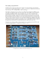
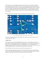
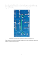
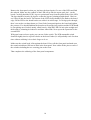
Oakley Sound Systems
Stereo Ensemble – SE330
PCB Issue 1
Builder's Guide
V1.0.9
Tony Allgood
Oakley Sound Systems
CARLISLE
United Kingdom
Introduction
This is the Builder's Guide for the issue 1 Stereo Ensemble Module SE330 from Oakley
Sound. This document contains a basic introduction to the circuit board and a full parts list for
the components needed to populate the board or boards.
For the User Manual, which contains an overview of the unit and goes into some detail
regarding the operation of the module, please visit the main project webpage at:
http://www.oakleysound.com/se330.htm
For general information regarding where to get parts and suggested part numbers please see
our useful Parts Guide at the project webpage or http://www.oakleysound.com/parts.pdf.
For general information on how to build our modules, including circuit board population,
mounting front panel components and making up board interconnects please see our generic
Construction Guide at the project webpage or http://www.oakleysound.com/construct.pdf.
This is an early version of the documentation. If you do find any errors, even silly little ones,
please do let me know either directly by e-mail or via the forum.
2
The Oakley Sound SE330
The SE330 does not have any built in power supply. It is expected that the circuit board be
powered from a regulated split supply of +/-12V to +/-17V. Power is admitted onto the board
via a four way 0.156” (2.96mm) header of MTA or KK type.
The module is designed to be powered by our own Rack Power Supply Unit (RPSU) or any
other split rail compatible supply such as the Oakley PSU. The benefits of using the RPSU is
its small size and ability to take a variety of different AC power sources. Because of the
inherent dangers of using a component level mains transformer in your project I recommend
that you use an external low voltage AC source such as that obtained from a wallwart or line
lump. The RPSU can then be fed from a low voltage alternating current supply so all the high
voltages are kept inside the wallwart or line lump. The User Manual for the RPSU will go into
more detail of the various options for powering your unit. A single RPSU should be capable of
driving both the HVM and SE330 should both projects be built into the same case.
The board size is 198mm (width) x 234mm (depth). Power consumption of the SE330, with
no audio passing through it, is +140mA and -110mA at +/-15V.
A completed issue 1 SE330 circuit board awaiting its case.
3
Parts List
For general information regarding where to get parts and suggested part numbers please see
our useful Parts Guide at the project webpage or http://www.oakleysound.com/parts.pdf.
The components are grouped into values, the order of the component names is of no particular
consequence.
A quick note on European part descriptions. R is shorthand for ohm. K is shorthand for kiloohm. So 22R is 22 ohm, 1K5 is 1,500 ohms or 1.5 kilohms. For capacitors: 1uF = one
microfarad = 1000nF = one thousand nanofarad.
To prevent loss of the small ‘.’ as the decimal point, a convention of inserting the unit in its
place is used. eg. 4R7 is a 4.7 ohm, 4K7 is a 4700 ohm resistor, 6n8 is a 6.8 nF capacitor.
NOTE: This board requires two track cuts to allow it to work as intended. These are
best done before you start to solder. Please see the Modifications section for the details
on how to do this.
Resistors
All resistors 1% 0.25W metal film resistors except where stated.
220R
390R
470R
510R
1K
3K3
4K7
6K8
7K5
10K
11K
15K
18K
22K
33K
36K
47K
56K
62K
R189, R190, R185, R87, R139, R179, R37, R184
R131, R150, R52, R128, R66, R49, R62, R146
R56
R145, R117, R115
R58
R153, R34, R136, R84, R176
R24, R99
R69, R8, R164, R101, R26, R116, R94, R93, R45, R7, R15
R118, R109, R143
R54, R161, R165, R181, R180, R172, R162, R134, R70, R40, R38,
R39, R174, R18, R16, R175, R55, R43, R32, R83, R82, R33, R135
R31, R171, R42, R79, R133
R48, R149, R47, R127, R129, R81, R75, R65, R151, R30, R41, R107,
R89, R92, R1, R126
R166, R72, R121, R19
R76, R59, R64, R3, R111, R124, R9, R154, R157, R160, R10, R60,
R12, R80, R108, R6, R13
R144, R112, R67, R120, R141, R50, R106, R36, R86, R178, R138
R17
R163, R102, R104, R96, R169, R170, R28, R5, R91, R27, R4, R173,
R159, R90
R53, R130, R63, R147
R14
4
100K
120K
150K
220K
470K
4M7 5%
R57, R168, R158, R110, R125, R148, R156, R152, R132, R68, R95,
R51, R123, R183, R61, R114, R182, R186, R140, R142, R21, R11,
R188, R187, R74, R46, R113
R88, R29, R105, R2
R177, R35, R85, R137
R71, R73, R20, R119, R44, R167, R78, R155, R122
R103, R100, R97, R25, R22, R23, R98
R77
Capacitors
Do not fit C61 just yet as the topside copper track next to it needs to be cut. See
modifications section for details.
Non-polar capacitors C119, C121, C122 and C123 are optional and can be replaced with wire
links. They are used as DC blocking (sometimes called audio coupling) capacitors and are
there to filter out unwanted steady state offset voltages from the final output amplifiers.
However, I found that the OPA2134 produces such a small offset as to warrant the use of
such capacitors superfluous.
100nF ceramic multilayer axial
C55, C92, C106, C78, C107, C110, C86, C109, C47,
C103, C19, C68, C82, C54, C83, C11, C65, C48, C24,
C22, C51, C25, C49, C20, C63, C50, C23, C12, C38,
C93, C36, C14, C37, C15, C13, C67, C64, C39, C111,
C66, C94, C85, C91, C108
100pF C0G ceramic 2.5mm
220pF C0G ceramic 2.5mm
470pF C0G ceramic 2.5mm
560pF C0G ceramic 2.5mm
C88, C95, C84, C2, C46, C57, C27, C34, C10, C113,
C69
C87, C56, C112, C18, C30, C26
C81, C17, C53, C105
C97, C79, C76
2u2, 63V electrolytic
10uF, 35V electrolytic
10uF non polar electrolytic
47uF, 25V electrolytic
C101, C100, C7, C73, C74, C42, C43, C8
C118, C117
C123, C119, C122, C121 – Optional, see note above.
C9, C102, C75, C44
1n5, 100V polyester
2n2, 100V polyester
6n8, 63V polyester
22nF, 63V polyester
100nF, 63V polyester
330nF, 63V polyester
470nF, 63V polyester
680nF, 63V polyester
1uF, 63V polyester
C52, C16, C104, C80, C33
C28, C31, C89, C114, C59
C77, C96, C61
C115, C60, C90, C29, C35
C1, C62
C45
C98, C71, C21, C5, C40, C58, C3, C70
C32
C116, C4, C72, C99, C6, C120, C41
5
Discrete Semiconductors
1N5819 Schottky diode
1N4148 small signal diode
1N4148 small signal diode
3.6V 500mW zener diode
BC550 NPN transistor
BC560 PNP transistor
Green or yellow 3mm LED
Red 3mm LED
D17, D18
D1, D2, D3, D5, D6, D7, D8, D9, D10, D11, D12,
D13, D14, D15, D16
To be soldered across R80. See modifications section.
Two required across R103. See modifications section.
Q9, Q4, Q11, Q13, Q8, Q14, Q12, Q3
Q5, Q6, Q10, Q2, Q1, Q7
ON
PEAK
D4 is not a diode but a wire link. Use a small piece of uninsulated wire like a resistor wire
clipping.
Integrated Circuits
78L09 +9V 100mA regulator
LM13700 dual OTA
V3102D Coolaudio BBD driver
BL3207 Coolaudio BBD
DG403 analogue switch
OPA2134PA dual op-amp
TL072 dual op-amp
V2164D quad VCA
U13, U33, U1, U24
U10, U21, U30, U2
U7, U18, U27, U36
U17, U35, U26, U6
U37, U20
U19, U40, U8, U39
U23, U11, U22, U15, U32, U38, U16, U29, U5, U34,
U12, U31, U9, U4, U25, U3, U14
U28
IC sockets are recommended. You need 29 8-pin DIL sockets and 7 16-pin DIL sockets.
Trimmers
20K or 22K 6mm
100K 6mm
4K7 or 5K 6mm
S_LVL, T_LVL
OFF1, OFF2, OFF3, OFF4, CLK1, CLK2, CLK3,
CLK4, T_FRQ, S_FRQ
NULL1, NULL2, NULL3, NULL4
Pots
All pots 16mm Alpha or Alps types.
47K or 50K linear dual gang
10K linear
47K or 50K linear
BALANCE, OUT_LEVEL
IN_LEVEL
TRI_RATE, TRI_DEPTH, SIN_RATE, SIN_DEPTH
Seven Alpha pot brackets. Seven knobs to suit.
6
Switch
SPDT (on-off-on) toggle switch
MODE
Interconnects
4 way 3.96mm Molex KK or MTA header
2 way 0.1” Molex KK or MTA header
3 way 0.1” Molex KK or MTA header
PSU
INPUT
OUT_L, OUT_R
The 2-way header DIRECT is unused.
1/4” TRS jack sockets (plastic frame)
3 off
Note:
Don't forget to solder a wire link in place of D4. Without this the peak LED won't work.
7
Required Modifications
The SE330 was a complex project so it was somewhat inevitable that working alone I would
end up making a few mistakes. It is typical, even on mass produced items, to find some degree
of re-working on any early issue PCB. Thankfully, my mistakes are pretty easy to rectify so
you dear builder will not have to alter the board too much. The tracking errors and missing
components will be corrected in any new issue of the board but given the cost of the first run
of SE330 boards it would be uneconomic and somewhat wasteful to dump them.
There are three modifications to do: Track cuts and jumper, the VCA maximum gain mod, and
the soft limiter mod.
Track Cuts
It is a rare thing to find a board design from me that requires track cuts, so it is with some
shame that I am asking you to do this. First you need to get a very sharp knife, the little
aluminium craft knives from X-acto and others are just the thing. Use a fresh blade as using a
blunt one can give poor results and is more likely to slip.
This is most easily done before you start to solder, however, it can be done with all the parts
in place except C61. On the topside of the board find C61's location. To the right of it you will
see a copper track in light blue heading from the top hole of C61 to a via hole in between the
TRI_DEPTH and SIN_RATE pots. You need to cut this track near C61. Make two cuts in
the track about 2mm apart from each other. Make sure the cuts go deep enough to slice
through the copper trace. Then with your knife peel back the section of trace between your
cuts. The tiny strip should peel off in one piece but it may need several picks to get it all out.
The topside track cut next to C61 as seen with the board populated.
8
The next track cut is on the underside but you will need to refer to the topside to find the
track you need to cut. Find R92, it's just above C61. Now flip the board over and locate the
lower solder pad of R92. You'll see a copper track coming from the square pad of U19 going
to the lower solder pad of R92 and then continuing down to a Y junction where one branch
goes to C61 and the other makes its way to R106. You need to cut the track between the
lower pad of R92 and the Y junction. Again make two cuts 2mm apart and peel off the little
piece of track.
You may wish to use a resistance meter to check that both tracks have been cut.
The second track cut. Ignore the two jumper wires for now.
You can now populate the board as described in the parts list. Once that is done you can
continue the modifications.
Jumper Wires
Now that we have cut the misplaced signals we now have to re-route them to the correct
places. This involves fitting two jumper wires. Both jumper wires are fitted to the underside of
the board. I use thin insulated solid core wire called Kynar wire. It's especially made for
making jumper connections on the backs of PCBs. However, you can use any type of wire you
like but the thinner solid core stuff is both neater and easier to work with.
The first jumper will connect the lower pad of R89 to the top pad of C61.
The second jumper will connect the lower solder pad of R92 to the lowest via pad between
the two pots, TRI_DEPTH and SIN_RATE. A via pad is the small solder pad that allows the
signal to normally be routed between the topside and bottom of the PCB.
9
I use a solder with an Ersin based flux as this makes soldering wires much easier than using
the usual no-clean solder. It does, however, make a little more mess, with visible flux left on
the board. This flux does no harm but can be removed with a propriety flux remover or a bit of
iso-propyl alcohol (IPA).
Both jumper wires in place. Note the pot brackets haven't been soldered in yet.
That completes the re-routing of the signals but there are two other modifications that need to
be done. See the next pages for details.
10
VCA maximum gain modification
In the parts list you'll see an additional 1N4148 diode. This is to be soldered across R80 on the
topside of the board. The cathode of the diode, marked with a dark band, should be facing
towards the front of the board. This modification prevents the VCAs in the noise reduction
unit from being driven too hard and allowing horrible noises to be heard.
The diode needs to be trimmed carefully and the legs preformed so it fits gracefully across and
above R80. There is no need to push it flat against the board. See photograph below.
The additional diode soldered across R80. Note also the wire link in position D4
Originally the modification was done with a BAT42 as can be seen in the photograph.
However, as soon as I implemented the 'soft limiter modification', as described overleaf, the
VCA's gain could be taken that much higher than the BAT42 allowed. Using a 1N4148, the
output of the VCA driver can be taken up to -600mV, which gives greater headroom for the
companding noise reduction but not too much as too create instability.
11
Soft limiter Modification
This modification instantaneously limits the signal level coming from the compressor that
forms part of the noise reduction circuitry. By doing this the four BBDs lines are stopped from
ever receiving really loud signals that would cause them to misbehave.
You need two 3.6V 500mW (0.5W) or 400mW (0.4W) zener diodes. These look very similar
to ordinary signal diodes. You need to twist their leads together so that their anodes are
connected together and the diode bodies form a Y shape. The cathode is denoted with a dark
band on the body of the diode so these should be at the non twisted ends. Then, cutting off
any excessive lead, solder the cathodes across R103 forming miniature upturned Y shape over
R103. Don't forget to solder the twist too and cut the twisted bit nice and short so it won't
stick up too far.
Two back to back zener diodes fitted across R103.
If you do make any other changes to the circuit do let the Oakley community know via our
friendly online forum at Muffwigglers. I, for one, am always interested to hear what people do
with their Oakley Sound projects.
12
Mounting the Pots, LEDs and Switches
A close up showing the two stereo (dual gang) pots, the power on LED and the three way toggle switch.
Note also the optional output capacitors that have simply been linked out.
If you are using the recommended Alpha pots then they can help support the PCB with the
addition of the specially manufactured pot brackets. However, given the large size of the
SE330 PCB it is also necessary to utilise some or all of the mounting holes at the edge of the
board. These holes are sized to take an M3 screw and can be used with suitable hex spacers to
fit the PCB directly to the lower panel of your case.
When constructing the board, temporarily fit the pot brackets to the pots by the nuts and
washers supplied with the pots. Now fit them into the appropriate holes in the PCB. But only
solder the three, or six, pins that connect to the pot. Do not solder the pot bracket at this
stage. When you have soldered all the pots you can fit the board to your front panel. Position
the PCB at right angles to the panel, the pot’s own pins will hold it fairly rigid for now. Then
you can solder each of the brackets. This will give you a very strong support and not stress the
pot connections.
The Alpha pots are labelled with an A, B or C suffix. For example: 50KB or 10KC. Alpha and
ALPS use the key; A = log, B = linear and C = reverse log. So a 50KB is a 50 kilohm linear
pot. Remember you can use 47K in place of a 50K pot.
The two board mounted LEDs must be fitted carefully if you are using the directly mounted
technique. Although this sounds fiddly, it's actually quite easy and it reduces wiring,
interference and possible errors.
13
Remove the front panel so that you just have the board again. Get one of the LEDs and find
the cathode. Make sure the cathode of the LED will go into the square pad, pin 1, on the
board. Carefully bend the LED’s legs at a point 6mm away from the plastic body of the LED.
The legs should be bent by 90 degrees so that the legs are pointing straight down. Check to
see if they fit into the board. The bottom of the LED’s body should fit just flush to the board
edge. Fit the LED to the board but do not solder it in at this stage. Let its legs poke through,
there’s no need to cut them down yet. Now fit the front panel again to the board and tighten
the pot nuts. You should find that the board now fits snugly into position and the LED should
be just poking out of its hole neatly, albeit loosely. Align the LED if it isn't quite straight and
then solder it, trimming its leads nice and short afterwards. Now repeat the operation for the
second LED.
With panel removed once again, you can now fit the switch. The PCB mountable switch
should fit tightly into its respective holes on the board. Indeed, it will probably work for short
time without soldering it in so don't forget to do so.
Make sure the switch body is flat against the board. Now refit the front panel and make sure
the round switch barrel fits into its hole in the front panel. Now solder all the pins on each of
the switches including the two securing pins to the front.
That completes the soldering of the front panel components.
14
Power Supply
Power is admitted onto the board using the usual Oakley power system. That is a single four
way 0.156” (3.96mm) MTA or Molex KK header. For the rack projects I am recommending
the Molex system over the MTA simply because the tool needed to make the interconnects is
much cheaper. It is also possible to solder the crimp terminals used in the KK system. It is, of
course, quite possible to solder your power leads straight onto the board.
The board is protected against reverse polarity with a couple of Schottky diodes. Note that
these diodes work by shorting out your power supply in the event of a reversal. Because of
this they should not be relied on if the reversal continues for a long time as this will stress both
the diodes and the power supply. The diodes are simply there to save the board's ICs from
certain death in the event of the power being inadvertently reversed or partially removed
during testing. There is no overvoltage protection so be careful not to put anything over +/17V into the board.
The pin out for the power connector, PSU:
Pin 1
Pin 2
Pin 3
Pin 4
+12V to +17V
Ground (0V)
Ground (0V)
-12V to -17V
Pin 1 is indicated by the little diagonal on the header's legend.
Both ground connections need not be connected to your power supply. However, you do
most certainly need at least one of them – either pin 2 or pin 3 will do if you using only one
connection.
A special compact low voltage supply has been made for this, and other Oakley rack projects,
in the form of the Oakley RPSU. You don't have to use this as any decent split rail supply will
do but it is an easy build and is flexible enough to suit most builders' needs. Please see the
RPSU Builder's Guide and User Manual for more details.
15
Inputs and Outputs
If you are building the suggested design then you have only one input and two outputs. Both
input and outputs are balanced and you should use TRS jack sockets. TRS, tip-ring-sleeve,
sockets are ones with three poles and are also used for headphone outputs.
Even though both input and outputs are balanced they are still compatible with unbalanced
signals. This means you can plug ordinary two pole mono jacks into the TRS sockets and the
unit will work as expected.
Audio projects should really be built into metal cases to prevent interference and because of
this we now face a bit of a conundrum. Ideally, balanced input and output sockets should be
grounded to the case. If you have internal mains transformer then the case will be grounded
via the power supply so this will ground the socket and any connecting cables. But this only
works if your sockets have a metal frame and can be guaranteed to make a permanent
electrical connection to the casing when they are tightened up. It also means that your PSU
must be grounding the case directly which, unlike with the internal mains transformer, is not
what I recommend when using an external wall wart.
Therefore I prefer to use plastic framed chassis mounted sockets for my rack projects. This
allows the case to be grounded via the power supply and keep the sleeve terminals of all the
sockets locally isolated from the case. Grounding the sockets must therefore be done via a
short wire link back to either the PSU's main ground star point (which is not so easily done on
the RPSU if both four way headers are being used) or the main SE330 PCB.
Input Socket
The two way header, named INPUT, should be wired so that pin 1 goes to the ring of the
input socket and pin 2 goes to the tip. Twist the wires together so that they form a simple
cable. The sleeve, or ground, of the input socket does not connect directly to the PCB but
should be connected to the sleeve terminal the left output socket.
Output Sockets
The three way headers, named OUT_L and OUT_R, should each be wired so that pin 1
connects to the tip of the relevant output socket and pin 3 goes to the ring. Again twist the
wires into pairs to form simple cables. The sleeve, or ground, terminal of left output socket
should go to the sleeve terminal of right output socket. This then connects back to the board
to pin 2 of the OUT_R header. Pin 2 of the OUT_L header is left unused.
16
Final Comments
If you have any problems with the module, an excellent source of support is the Oakley Sound
Forum at Muffwiggler.com. Paul Darlow and I are on this group, as well as many other users
and builders of Oakley modules.
I'd love to hear about what you have done with your module. Please do post pictures of your
finished module at the Oakley Sound forum on Muffwiggler.
And if you can't get your project to work, then Oakley Sound Systems are able to offer a 'get
you working' service. If you wish to take up this service please e-mail me, Tony Allgood, at
my contact e-mail address found on the website. I can service either fully populated PCBs or
whole modules. You will be charged for all postage costs, any parts used and my time at
25GBP per hour. Most faults can be found and fixed within one hour, and I normally return
modules within a week. The minimum charge is 25GBP plus return postage costs.
If you have a comment about this user guide, or have a found a mistake in it, then please do let
me know. But please do not contact me or Paul Darlow directly with questions about sourcing
components or general fault finding. Honestly, we would love to help but we do not have the
time to help everyone individually by e-mail.
Last but not least, can I say a big thank you to all of you who helped and inspired me. Thanks
especially to all those nice people on Muff's Forum and the Synth-diy and Analogue Heaven
mailing lists.
Tony Allgood at Oakley Sound
Cumbria, UK
© August 2013 – updated September 2013
No part of this document may be copied by whatever means without my permission.
17