1
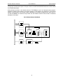
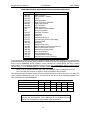
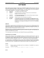
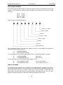
1781-PXB1201
120-POINT DIGITAL INPUT/OUTPUT CARD
User’s Manual
Western Reserve Controls, Inc.
1
Western Reserve Controls
1781-PXB1201
User’s Manual
Although every effort has been made to insure the accuracy of this document, all information is subject to
change without notice. WRC takes no liability for any errors in this document or for direct, indirect,
incidental or consequential damage resulting from the use of this manual.
The information in this document is provided for reference only. WRC does not assume any liability
arising out of the application or use of the information or products described herein. This document may
contain or reference information and products protected by copyrights or patents and does not convey any
license under the patent rights of WRC, nor the rights of others.
WRC is a trademark of Western Reserve Controls, Inc.
IBM PC, PC/XT, and PC/AT are registered trademarks of the International Business Machines
Corporation.
Printed in the USA.
Copyright © 1998, 1999 WRC
Western Reserve Controls, Inc.
526 South Main Street, Suite 310
Akron OH 44311
330-762-1611 (Phone)
330-762-1622 (FAX)
[email protected] (Email)
http://www.wrcakron.com (Web)
Western Reserve Controls
1781-PXB1201
User’s Manual
TABLE OF CONTENTS
INSTALLATION............................................................................................................................................ 2
BACKING UP THE DISK ................................................................................................................. 2
HARD DISK INSTALLATION........................................................................................................... 2
INSTALLING THE CARD................................................................................................................. 2
FUNCTIONAL DESCRIPTION ..................................................................................................................... 4
BLOCK DIAGRAM ........................................................................................................................... 5
OPTION SELECTION................................................................................................................................... 6
OPTION SELECTION MAP ............................................................................................................. 7
ADDRESS SELECTION ............................................................................................................................... 8
ADDRESS ASSIGNMENTS FOR PC XT ........................................................................................ 8
ADDRESS ASSIGNMENTS FOR 286/386/486............................................................................... 9
SOFTWARE................................................................................................................................................ 10
PXB120ST....................................................................................................................................... 10
VISUALBASIC UTILITY DRIVER................................................................................................... 10
PROGRAMMING ........................................................................................................................................ 12
PORT ADDRESS SELECTION TABLE......................................................................................... 12
PROGRAMMING EXAMPLE ......................................................................................................... 14
SAMPLE PROGRAMS................................................................................................................... 14
SHARING INTERRUPTS ON THE ISA BUS................................................................................. 21
CONNECTOR PIN ASSIGNMENTS .......................................................................................................... 22
SPECIFICATIONS ...................................................................................................................................... 23
1
Western Reserve Controls
1781-PXB1201
User’s Manual
INSTALLATION
BACKING UP THE DISK
The software provided with the 1781-PXB1201 is in MS-DOS format on diskette. As with any software
package, you should make backup copies for everyday use and place your original master diskette in a
safe location.
The easiest way to make a backup copy is to use the DOS DISKCOPY utility.
In a single-drive system the command is:
DISKCOPY A: A:
In a two-disk system the command is:
DISKCOPY A: B:
This will copy the contents of the master disk in drive A to the backup disk in drive B.
HARD DISK INSTALLATION
The files contained on the master diskette may also be copied onto your hard disk. To do this perform the
following:
1.)
2.)
3.)
Place the master diskette into a floppy drive.
Change the active drive to the drive that has the master diskette installed. For example, if
the diskette is the A drive, type A:
Type INSTALL and follow the screen prompts.
Files contained on the disk are stored in separate directories as follows:
ROOT DIRECTORY:
Contains the FINDBASE PROGRAM that will help you to decide what base
address to use with the card. Also contains the PXB1201ST.EXE setup program.
PSAMPLES:
CSAMPLES:
BSAMPLES:
Contains Pascal samples and the Pascal-linkable driver.
Contains "C" samples and the "C"-linkable driver.
Contains the BASIC and QuickBASIC samples as well as the binary and linkable
drivers.
VisualBASIC utility driver that includes PEEK and POKE statements for reading
and writing RAM as well as OUTPORT and INPORT for reading and writing port
I/O. The driver is in the form of a DLL and allows you to access hardware as if
the language was designed for it when you use VisualBASIC for Windows.
VB_WRC:
INSTALLING THE CARD
Before installing the card carefully read the ADDRESS SELECTION and OPTION SELECTION sections
of this manual and configure the card according to your requirements. Use the special software program
called PXB1201ST provided on diskette with the card. It supplies visual aids to configure all areas of the
board.
Be especially careful with address selection. If the addresses of two installed functions overlap, you will
experience unpredictable computer behavior. If unsure what locations are available, you can use the
FINDBASE program provided on our diskette to locate blocks of available addresses.
2
Western Reserve Controls
1781-PXB1201
User’s Manual
To install the card:
1. Remove power from the computer.
2. Remove the computer cover.
3. Remove blank I/O backplate.
4. Install jumpers for selected options. See the OPTION SELECTION section of this manual.
5. Select the base address on the card. See the ADDRESS SELECTION section of this manual.
6. Loosen the nuts on the strain relief bar and swing top end free.
7. Install the card in an I/O expansion slot. If convenient, select a slot, which is adjacent to a vacant
slot, because this will make cable installation easier.
8. Thread the I/O cables, one by one through the cutout in the mounting bracket and plug them into
the headers.
9. Smooth the cables as close as practicable to the card and while holding them close to the card
surface, swing the strain relief bar into position and tighten nuts.
10. Inspect for proper fit of the card and cables and tighten screws. Make sure that the mounting
bracket is properly screwed into place and that there is a positive chassis ground.
11. Replace the computer cover.
Input/Output connections are via five 50-pin headers on the card. A blank mounting bracket is provided
with units that are marked for CE (European) Certification and, for these units, CE-certifiable cable and
break-out methodology (cables connected to ground at the aperture, shielded twisted pair wiring, etc.)
must be used.
3
Western Reserve Controls
1781-PXB1201
User’s Manual
FUNCTIONAL DESCRIPTION
FEATURES
120 Channels of Digital Input/Output.
All 120 I/O Lines Buffered on the Board.
Four and Eight Bit Groups Independently Selectable for I/O.
Hysteresis Correction and Pull-Down Resistors on I/O Lines.
Interrupt and Interrupt-Disable Capability.
Tri-stateable I/O ports under software control.
+5V Supply Available to User.
Compatible with Industry Standard I/O Racks from WRC, others such as Gordos, Opto-22, Potter &
Brumfield, etc.
APPLICATIONS
Automatic Test Systems.
Security Systems, Energy Management.
Robotics
Relay Monitoring and Control.
Parallel Data Transfer to PC.
Sensing switch closures or TTL, DTL, CMOS Logic.
Driving Indicator Lights or Recorders.
The 1781-PXB1201 board was designed for industrial applications and should be installed in a long slot of
an IBM PC/XT/AT or compatible computer. Each I/O line is buffered and capable of sourcing 15mA, or
sinking 24mA (64mA on request). The board contains five Programmable Peripheral Interface chips type
8255-5 (PPI) to provide computer interface to 120 digital I/O lines. Each PPI provides three 8-bit ports A,
B, and C. Each 8-bit port can be configured to function as either inputs or output latches. Port C can also
be configured as four inputs and four output latches. The I/O line buffers (74LS245) are configured
automatically by hardware logic for input or output use according to the PPI 8255-5 Control Register
direction software assignment.
The I/O buffers may be tristated under program control. If the BEN/TST jumper on the card is installed in
the BEN position, the I/O buffers are permanently enabled allowing transparent backwards compatibility.
However, if the jumper is placed in the TST position, enable/disable of the buffers is possible under
software control.
Two I/O lines of each port can be used for interfacing User Interrupts to the computer. Interrupts are
buffered and are enabled by jumper installation or by a combination of jumper installation and a digital
input line. You can use Interrupts #2 through #7, #10 through #12, #14 and #15. Interrupts of all ports
(one per port) are OR'ed together. I/O wiring connections are via 50-pin headers on the board. Five flat
I/O cables connect the 1781-PBX1201 to digital mounting boards such as WRC’s 1781-Axxx. Also, this
provides compatibility with Dataforth, Crydom, OPTO-22, Gordos, Potter & Brumfield, etc. module
mounting racks. Every second conductor of the flat cables is grounded to minimize the effect of crosstalk
between signals. If needed for external circuits +5VDC power is available on each I/O connector pin 49.
If you use this power, we recommend that you include a 1A fast blow fuse in your circuits in order to
avoid possible damage to the host computer.
The board occupies thirty-two consecutive bytes within the I/O address space. The base address is
selectable via ADDRESS SETUP DIP switches (A5-A9) anywhere within the hex 000-3FF range.
However, if 96 or less I/O lines are to be used, then the 1781-PXB1201 board can be configured to
4
Western Reserve Controls
1781-PXB1201
User’s Manual
occupy only 16 consecutive bytes of I/O space. Refer to the OPTION SELECTION Section of this manual
for a detailed description.
Utility software provided on the diskette with the 1781-PXB1201 card is an illustrated setup program.
Interactive displays show locations and proper settings of DIP switches and jumpers to set up board
address, interrupt levels, and interrupt enable. Additionally, two sample programs and a utility driver for
use with VisualBASIC for Windows are provided. See the Software section of this manual for a detailed
description of the latter.
1781-PXB1201 BLOCK DIAGRAM
5
Western Reserve Controls
1781-PXB1201
User’s Manual
OPTION SELECTION
Refer to the illustrated setup programs on the diskette provided with the card when reading this section of
the manual. Also, refer to the OPTION SELECTION MAP on the following page.
The card comes with jumpers installed at locations marked 120 and 120B. These enable all 120 I/O lines
on the card. If 32 bytes of I/O space is not available and 96 or less I/O lines are to be used, then it is
possible to configure the card to occupy only 16 bytes in I/O space. This will disable Port 4. To select this
option, move the two jumpers to the locations marked 96 and 96B.
Base address selection is covered both by the diskette and in the next section of this manual.
Interrupts are accepted on the I/O connector, pin 9 (port C3). The interrupt signal is positive true. Interrupts are unconditionally enabled if the IEN jumper is installed, or enabled by program if the INP jumper is
installed and I/O connector pin 1 (port C) is low. Interrupts are disabled if (a) neither the IEN or INP jumper
is installed, or (b) if the INP jumper is installed but I/O connector pin 1 (port C7) is held high. User
interrupts are directed to interrupts #2 through #7, #10 through #12, #14 and #15 by jumpers installed at
locations labelled IRQ2 through IRQ15.
The foregoing are the only manual setups necessary to use the 1781-PXB1201. Input/Output selection is
done, via software, by writing to the PPI 8255-5 Control Registers as described in the PROGRAMMING
section of this manual.
1781-PXB1201 provides a means to enable/disable the tristate I/O buffers under program control. If the
BEN/TST jumper on the card is installed in the BEN position, the I/O buffers are permanently enabled.
However, if the jumper is placed in the TST position, enable/disable of the buffers is possible under
software control via the Control Register as described in the Software Programming section of this
manual.
6
Western Reserve Controls
1781-PXB1201
OPTION SELECTION MAP
7
User’s Manual
Western Reserve Controls
1781-PXB1201
User’s Manual
ADDRESS SELECTION
The 1781-PXB1201 Input/Output Card occupies 32 bytes of I/O space. The card base address can be
selected anywhere within an I/O address range 000-3FF hex. If all 120 bits are to be used in an AT-class
computer, the base address can be set anywhere within the address range hex 100-390 (except 1F0
through 1F8). If only 96 bits are to be used, the base address can be anywhere in the range hex 100-3F0.
If to be used in an XT-class computer, the starting address can be as above except the lowest starting
address is 200 hex.
However two installed options can not share the same address. If in doubt where to assign the base
address of the 1781-PXB1201, refer to the tables below and consult the FINDBASE program on the utility
diskette.
STANDARD ADDRESS ASSIGNMENTS FOR PC XT COMPUTERS
Hex Range
000-00F
020-021
040-043
060-063
080-083
0AX
0CX
OEX
100-1FF
200-20F
210-217
220-24F
278-27F
2F0-2F7
2F8-2FF
300-31F
320-32F
378-37F
380-38C**
380-389**
3A0-3A9
3B0-3BF
3C0-3CF
3D0-3DF
3E0-3E7
3F0-3F7
3F8-3FF
Usage
DMA Chip 8237A-5
Interrupt 8259A
Timer 8253-5
PPI 8255A-5
DMA Page Register
NMI Mask Register
Reserved
Reserved
Not Usable
Game Control
Expansion Unit
Reserved
Reserved
Reserved
Asynchronous Comm'n (Secondary)
Prototype Card
Fixed Disk
Printer
SDLC Communications
Binary Synchronous Comm. (Secondary)
Binary Synchronous Comm. (Primary)
IBM Monochrome Display/Printer
Reserved
Color/Graphics
Reserved
Diskette
Asynchronous Comm'n (Primary)
** These options can not be used together - addresses overlap
8
Western Reserve Controls
1781-PXB1201
User’s Manual
STANDARD ADDRESS ASSIGNMENTS FOR 286/386/486 COMPUTERS
Hex Range
Usage
000-01F
020-03F
040-05F
060-06F
070-07F
080-09F
0A0-0BF
0C0-0DF
0F0
0F1
0F8-0FF
1F0-1F8
200-207
278-27F
2F8-2FF
300-31F
360-36F
378-37F
380-38F
3A0-3AF
3B0-3BF
3C0-3CE
3D0-3DF
3F0-3F7
3F8-3FF
DMA Controller 1
INT Controller 1, Master
Timer
8042 (Keyboard)
Real Time Clock, NMI Mask
DMA Page Register
INT Controller 2
DMA Controller 2
Clear Math Coprocessor Busy
Reset Coprocessor
Arithmetic Processor
Fixed Disk
Game I/O
Parallel Printer Port 2
Asynchronous Comm'n (Secondary)
Prototype Card
Reserved
Parallel Printer Port 1
SDLC or Binary Synchronous Comm'n 2
Binary Synchronous Comm'n 1
Monochrome Display/Printer
Local Area Network
Color/Graphic Monitor
Floppy Diskette Controller
Asynchronous Comm'n (Primary)
To set desired board address, refer to the illustrated Board Address setup program on the Utility diskette
provided with the card. Type the desired address in hexadecimal code and the graphic display shows you
how to set the ADDRESS SETUP switches. These switches are marked A4-A9 and form a binary
representation of the address in negative-true logic. Assign '0' to all ADDRESS SETUP switches turned
ON, and assign '1' to all ADDRESS SETUP switches turned OFF.
NOTE: The A4 switch is enabled only if the 1781-PXB1201 card is configured for 96 I/O
lines. The card then occupies 16 bytes of I/O space instead of the normal 32.
The following example illustrates switch selection corresponding to hex 2D0 (or binary 10 1101 xxxx) The
"xxxx" represents address lines A3, A2, A1, and A0 used on the card to select individual registers at the
PPI's. See Section 6, PROGRAMMING.
Hex Representation
Conversion Multipliers
Binary Representation
Setup
Switch ID
2
2
1
OFF
A9
D
1
0
ON
A8
8
1
OFF
A7
4
1
OFF
A6
2
0
ON
A5
1
1
OFF
A4
CAUTION: Review the address selection reference table carefully before
selecting the card address. If the addresses of two installed functions
overlap you will experience unpredictable computer behavior.
9
Western Reserve Controls
1781-PXB1201
User’s Manual
SOFTWARE
WRC supplies several programs to support the 1781-PXB1201 Digital I/O card and, also, to help you
develop your applications software. These programs are on a diskette that comes with your card and
consist of a Setup program and three sample programs. The sample programs are in forms suitable for
use with BASIC, QuickBASIC, C, and Pascal. The programs as follows:
!
PXB120ST
1781-PXB1201 Board Setup Program
!
"
SAMPLE1
"
A program that writes a sequence of values to Port A and reads and
displays the values in Ports A & B.
!
"
SAMPLE2
"
A "C" program that displays the bits in Ports A & B and, when an interrupt
occurs, polls those same bits.
!
FINDBASE
Program locates active and available port addresses.
!
VB_WRC
"
A VisualBASIC utility driver that includes PEEK and POKE statements for
reading and writing RAM as well as INPORT and OUTPORT for reading
and writing I/O. The driver is in the form of a DLL and allows you to access
hardware as if the language was designed for it when you use VisualBASIC
for Windows.
PXB120ST
This program is supplied with the 1781-PXB1201 card as a tool for you to use in configuring jumpers and
switches on the card. It is menu-driven and provides pictures of the card on the computer monitor. You
make simple keystrokes to select the functions. In turn, the pictures then change to show how the
jumpers or switches should be placed to effect your choices.
The setup program is a stand-alone program that can be run at any time. It does not require the 1781PXB1201 to be plugged into the computer for any part of the setup. The program is self-explanatory with
operation instructions and on-line help.
To run this program, at the DOS prompt, enter PXB120ST followed by the [ENTER] key.
VISUALBASIC UTILITY DRIVER
WRC provides extensions to the VisualBASIC language on the diskette provided with your card. The
extensions are in a directory named VB_WRC. These extensions are in the form of a .DLL, a .GBL, and
a VisualBASIC sample. Together these files allow you to access the port and main memory space in a
++
fashion similar to BASIC, QuickBASIC, Pascal, C/C , Assembly, and most other standard languages.
To use these files in a VisualBASIC program, you must create a .MAK file (File l New Project) similar to
the sample provided (or else, modify your existing project file) and include the .GBL file (File | Add File).
Once this has been done, VisualBASIC will be enhanced with the addition of the following functions.
InPortb
Function:
Reads a byte from a hardware port. Due to limitations of VisualBASIC, the number is
returned in an integer.
Declaration:
function InPortb(byval address as integer) as integer
InPort
10
Western Reserve Controls
1781-PXB1201
User’s Manual
Function:
Reads an integer from a hardware port. This function returns the 16-bit value obtained
from reading the low byte from address and the high byte from address+1.
Declaration:
function InPort(byval address as integer) as integer
OutPortb
Function:
Writes the lower eight bits of value to the hardware port at address. This function returns
the value output.
Declaration:
function OutPortb(byval
integer) as integer
address
as
integer,
byval
value
as
OutPort
Function:
Writes all 16 bits of value to the hardware port at address. This function returns the value
output.
Declaration:
function OutPort(byval
integer) as integer
address
as
integer,
byval
value
as
Peek
Function:
Reads a byte from main memory (DRAM).
Declaration:
function Peek(byval segment as integer, byval offset as integer)
as integer
Poke
Function:
Writes the lower eight bits of value to segment:offset.
Declaration:
function Poke(byval segment as integer, byval offset as integer,
byval value as integer) as integer
Note that in all of the above functions, an inherent limitation of BASIC in general and VisualBASIC in
particular makes the values sent less intuitive. All integers in BASIC are signed numbers, wherein data
are stored in two's complement form. All bit patterns must be converted to-and-from this two's
complement form if meaningful display is required. Otherwise, values returned from the InPortb function
will be -128 to 127, rather than 0 to 255. An alternative is to perform all assignments in hexadecimal,
rather then decimal form.
Before the program will execute, the .GBL file must be modified to include the path to the VB_WRC.DLL
as appropriate for your system. Merely replace the statement "VB_WRC.DLL" with
"drive:path\VB_WRC.DLL".
As an alternative to changing the source code, you can copy the VB_WRC.DLL file into your Windows
directory. This will allow multiple programs to find the same .DLL without having to know where it is
located. Just omit all references to a path in the .GBL file as shown in the sample.
11
Western Reserve Controls
1781-PXB1201
User’s Manual
PROGRAMMING
The 1781-PXB1201 is an I/O mapped device that is easily configured from any language and any
language can easily perform digital I/O through the card's ports. This is especially true if the form of the
data is byte or word wide. All references to the I/O ports would be in absolute port addressing. However,
a table could be used to convert the byte or word data ports to a logical reference.
DEVELOPING YOUR OWN SOFTWARE
If you wish to gain a better understanding of the programs listed in the previous section, then the
information in the following paragraphs will be of interest to you. Follow the 8255-5 Specification in
APPENDIX A to program the PPI's on the 1781-PXB1201 Digital Input/Output Card.
A total of 20 address locations are used by the 1781-PXB1201 for addressing the PPI's; four for each
PPI. The PPI's are addressed using address bits A3 through A0 (See Address Selection, section 4 of this
manual.) as follows:
PORT ADDRESS SELECTION TABLE
Address
Base Address
Base Address +1
Base Address +2
Base Address +3
Base Address +4
Base Address +5
Base Address +6
Base Address +7
Base Address +8
Base Address +9
Base Address +A
Base Address +B
Base Address +C
Base Address +D
Base Address +E
Base Address +F
Base Address +10
Base Address +11
Base Address +12
Base Address +13
Port Assignment
Operation
PA Port 0
PB Port 0
PC Port 0
Control Port 0
PA Port 1
PB Port 1
PC Port 1
Control Port 1
PA POrt 2
PB Port 2
PC Port 2
Control Port 2
PA Port 3
PB Port 3
PC Port 3
Control Port 3
PA Port 4
PB Port 4
PC Port 4
Control Port 4
Read/Write
Read/Write
Read/Write
Write Only
Read/Write
Read/Write
Read/Write
Write Only
Read/Write
Read/Write
Read/Write
Write Only
Read/Write
Read/Write
Read/Write
Write Only
Read/Write
Read/Write
Read/Write
Write Only
The 1781-PXB1201 uses five 8255-5 PPI's to provide a total of 120 bits input/output capability. The card
is designed to use each of these PPI's in mode 0 wherein:
a)
b)
c)
d)
There are two 8-bit ports (A and B) and two 4-bit ports (C Hi and C Lo).
Any port can be configured as an input or an output.
Outputs are latched.
Inputs are not latched.
Each PPI contains a control register. This Write-only, 8-bit register is used to set the mode and direction
of the ports. At Power-Up or Reset, all I/O lines are set as inputs. Each PPI should be configured during
initialization by writing to the control registers even if the ports are going to be used as inputs. Output
buffers are automatically set by hardware logic according to the control register. Control registers are
12
Western Reserve Controls
1781-PXB1201
User’s Manual
located at base addresses +3, +7, +B, +F, and +13. Bit assignments in each of these control registers
are as follows:
Bit
Assignment
Function
D0
D1
D2
D3
D4
D5,D6
Port C Lo (C0-C3)
Port B
Mode Selection
Port C Hi (C4-C7)
Port A
Mode Selection
D7
Mode Set Flag
1 = Input, 0 = Output
1 = Input, 0 = Output
1 = Mode 1, 0 = Mode 0
1 = Input, 0 = Output
1 = Input, 0 = Output
01 = Mode 1, 00 = Mode 0
1X = Mode 2
1 = Active
NOTE: Contact WRC for directions if you wish to operate this card in
mode 1. This card cannot be operated in mode 2
1781-PXB1201 provides a means to enable/disable the tristate I/O buffers under program control. If the
BEN/TST jumper on the card is installed in the BEN position, the I/O buffers are permanently enabled.
However, if the jumper is placed in the TST position, enable/disable of the buffers is possible under
software control via the Control Register as follows:
1. The card is initialized in the receive mode by the computer Reset command.
2. When bit D7 of the Control Register is set high, the direction of the three ports of the associated PPI
chip as well as the mode can be set. For example, a write to Base Address+3 with data bit D7 high
programs port direction of Port 1 ports A, B, and C. If, for example, hex 80 is sent to Base
Address+3, the Port 0 PPI will be configured in mode 0 with ports A, B, and C as outputs.
But, at the same time, data bit D7 is also latched in a buffer controller for the associated PPI chip. A high
state disables the buffers and, thus, all associated buffers will be put in the tristate mode; i.e., disabled.
3. When you wish to enable the output buffers, send a normal PPI mode command with bit D7 low.
For, example, if a control byte of hex 80 had been sent as previously described, and it is now desired
to open the three ports, you can send a control byte of hex 00 to Base Address+3 to enable the port
0 buffers.
4.
Those buffers will now remain enabled until another control byte with data bit D7 high is sent to Base
Address+3.
Those buffers will now remain enabled until another control byte with data bit D7 high is sent to Base
Address +3.
NOTE: All data bits except D7 must be the same for the two control bytes
13
Western Reserve Controls
1781-PXB1201
User’s Manual
PROGRAMMING EXAMPLE
The following programming example is provided as a guide to assist you in developing your working
software. In this example, the card base address is 2D0 hex and I/O lines of Port 0 are to be setup
as follows:
port A
port B
port C hi
port C lo
= Input
=Output
= Input
=Output
Configure bits of the Control Register as:
D7
D6
D5
D4
D3
D2
D1
D0
1
0
0
1
1
0
0
0
|
|
|
|
|
|
|
|
|
|
|
|
|
|
|
|____ Port C Lo = output
|
|
|
|
|
|
I
|
|
|
|
|
|
|_________ Port B = output
|
|
|
I
I
|
|
|
|
|
|
|______________ Mode 0
|
|
|
|
|
|
|
|
|
|___________________ Port C Hi = input
|
|
|
|
|
|
|
|________________________ Port A = input
|
|
|
|
|
|_____________________________ Mode 0
|
|
|
|__________________________________ Mode 0
|
|_______________________________________ Active Mode Set
This corresponds to 98 hex. If the card base address is 2D0 hex, use the BASIC OUT command to
write to the control register as follows:
10
20
BASEADDR=&H2D0
OUT BASEADDR+3,&H98
To read the inputs at Port A and the upper nybble of Port C, use the BASIC INPUT command:
30
40
X=INP(BASEADDR)
Y=INP(BASEADDR+2)/16
'Read Port A
'Read Port C Hi
To set outputs high ("1") at Port B and the lower nybble of Port C:
50
60
OUT BASEADDR+1,&HFF
OUT BASEADDR+2,&HF
'Turn on all Port B bits
'Turn on all bits of Port C Lo
SAMPLE PROGRAMS
The following sample programs are in TURBO-C and TURBO-PASCAL languages. They cover a
security system that allows you to monitor the status of 16 switches and to automatically trigger four
alarms that can be used to turn on lights, activate a siren, or send a signal to a silent alarm. The
alarm system in this demonstration has four arming stations which toggle the alarm on or off. These
programs are also provided on the diskette that WRC supplied with your IOD card.
14
Western Reserve Controls
1781-PXB1201
User’s Manual
TURBO-PASCAL PROGRAM
CONST BASEADDR = $300;
CONST ON
= 1;
CONST OFF
= 0;
{declare base address for IOD card}
{declare some useful constants}
{
"
"
"
"
}
TYPE sensor_array = array[0..15] of integer; {creates a type of variable}
{used for sensor data}
VAR sensors_at_arm : sensor_array; {bit-by-bit status of sensors when}
{alarm is activated. Used to notify}
{user of open windows, etc}
VAR sensors_now : sensor_now;
{bit-by-bit status of sensors at}
{current time. When compared against}
{sensors_at_arm, indicates break-in if}
{there is a change.}
VAR arming_stations : integer;
{variables representing all four arming}
{stations}
VAR old_arming_stations: integer;
{If value changes toggle alarm on/off}
VAR hour, min., sec., hun. : word; {variables used to retrieve time}
VAR key : char;
{useful temporary variable}
VAR i : integer;
{useful temporary variable, used in}
{loops}
VAR j : integer;
{useful temporary variable, used in}
{loops}
procedure initialize_board;
{this procedure sets MODE 0 as active}
{and sets ports A, B, and C LO as input}
{and port C HI as output}
begin
port[BASEADDR+3] :=$93;
{port[X] is Pascal's method of}
{accessing the port memory. This code}
{sets the port memory at address 303}
{hex, and the control register, to 93}
{hex because the bit pattern to set the}
{desired mode and port designations is}
{10010011 which equals 93 hex}
end;
{procedure initialize_board}
procedure read_sensors(VAR ary:sensor_ary);
VAR tempA : byte;
{this procedure fetches data from ports}
VAR tempB : byte;
{A and B and returns a binary}
{representation of each sensor}
begin
tempA := port[BASEADDR];
{this procedure loads tempA and tempB}
{with corresponding inputs from the}
{card}
tempB := port[BASEADDR+1];
for i := 0 to 7 do begin
if ((tempA shr i) AND ON) > 0 then {this tests to see if bit #i}
ary[i]:=ON
{is ON and sets the corresponding array
{element to ON if it is}
else
{else, the array element is set to OFF}
ary[i]:=OFF
end;
for i:=0 to 7 do begin
if ((tempB shr i) AND ON) > 0 then
ary[i+8]:=ON
{in order to get port B into}
{array, elements 8 thru 15, we}
else
{add 8 to the bit numbers in the}
ary[i+8]:=OFF;
{assignment}
end;
15
Western Reserve Controls
1781-PXB1201
end;
function get_status:integer;
var temp:integer;
begin
temp:=port[BASEADDR+2];
get_status:=temp AND $0F;
User’s Manual
{procedure read_sensors}
{this sets status to the lower}
{nibble of the half defined by}
{Initialize to be input for four}
{arming switches}
{function get_arming_status}
end;
procedure ALARM
var temp:longint;
begin
sound(2000);
{this starts the computer's}
{speaker which acts as siren for
{the alarm}
temp:=0
port[BASEADDR+2]:=$F;
{this sets port C's lower nibble}
{bits to ON}
repeat
arming_stations:=get_status
end;
begin
{this activates four alarm}
{outputs and then}
if arming_stations <> old_arming_stations then {toggles port C}
{Hi's LSB which might be used}
temp:=2000000000;
{with an external siren}
port[BASEADDR+2]:=port[BASEADDR+2] XOR $10;
temp:=temp+1;
until temp>=2000000000;
nosound;
{procedure ALARM}
initialize_board;
clrscr;
gotoxy(5,5);
writeln('This is the IOD card demonstration program. This ');
writeln('program will simulate an alarm system program for ');
writeln('sixteen sensors and four arming stations, along with');
writeln('four separate alarm outputs which could be routed to');
writeln('a siren, lights, silent alarm,etc');
writeln;
writeln('THIS PROGRAM IS INTENDED FOR DEMONSTRATION PURPOSES,');
writeln('ONLY AND IS NOT MEANT TO BE USED AS AN ACTUAL ALARM ');
writeln('SYSTEM.');
writeln;writeln;
writeln('Press any key to begin program.');
key:readkey;
old_arming_stations:=get_status;
{this loads the status of the}
{arming switches at the time the}
repeat
{program is first activated. A}
{change in status would indicate}
{arming}
read_sensors(sensors_now);
{this reads the current status of}
{the sensors which is then}
for i=0 to 15 do begin
{displayed to indicate open}
if sensors_now[i]=OFF then
{windows, etc}
writeln('Sensor #',i,'is open');
end;
writeln;
writeln('Press ESC to re-scan, RETURN to begin scanning.');
clrscr;
16
Western Reserve Controls
1781-PXB1201
key:=readkey;
until key=#13;
User’s Manual
{the repeat/until loop gives the}
{user an opportunity to shut open}
{windows or doors and then
{re-scan the sensors}
clrscr;
WHILE TRUE do begin
{this WHILE is used to form an infinite loop}
writeln('Waiting to be armed, or press any key to halt program.');
repeat
{this repeat/until-loop continues
{until arming}
arming_stations:=get_status; {station status changes,}
{indicating arming}
if key pressed then halt(1); {arming, or until a key is}
{pressed terminatingthe program}
until arming stations <> old arming stations;
sound(900);
{short tone indicating alarm has been armed}
delay(300);
{ "
"
"
"
"
"
" }
nosound;
{ "
"
"
"
"
"
" }
writeln('Alarm system will activate in 15 seconds');
read_sensors(sensors_at_arm);
old_arming_stations : get_status;
gettime(hour,min,sec,hun);
{this code reads the system clock}
i:=sec+15;
{for the current time which is}
if i > 60 then i :=i-60;
{used to delay for 15 seconds}
repeat
gettime(hour,min,sec,hun);
until sec = i;
{end of delay loop}
writeln;
writeln('ALARM SYSTEM ACTIVE AND ARMED');
sound(900);
{short tone indicating that alarm}
delay(300);
{is fully activated}
no sound;
j:=0
{the following code compares}
{current status of sensors}
{against status when armed to}
{determine if break-in has}
{occurred.. Any change indicates
{break-in}
repeat
read_sensors(sensors_now);
for i:= 1 to 16 do begin
if sensors_now[i-1] <> sensors_at_arm[i-1]then
j:=1;
end;{for}
arming_stations: get_status;
if arming_stations <> old_arming_stations then
j:= -i;
{flag used to signal that alarm}
{is de-activated}
until j <> 0;
if j = -1 then begin
{if j was set to -1 in the above}
{loop, then alarm is de-activated}
gettime(hour,min,sec,hun);
writeln('Alarm deactivated at ', hour,':',min,':',sec);
sound(900);
{the following code chirps the}
{speaker to indicate disarming}
delay(100);
no sound;
17
Western Reserve Controls
1781-PXB1201
User’s Manual
delay(50);
sound(900);
delay(100);
nosound;
end
{end of disarming routine}
else {if alarm}begin
writeln('Sensor #', j,' has been activated!!');
gettime(hour,min,sec,hun);
writeln('The time of alarm is ',hour,':',min,':',sec);
ALARM;
end;
{else}
end;
{WHILE this "end" sends the}
{program back to wait to be}
{re-armed}
end.
TURBO-C PROGRAM
#define BASEADDR 0x300
#define ON
1
#define OFF
0
#include "stdio.h"
#include "conio.h"
#include "time.h"
#include "dos.h"
int sensors_at_arm[15];
int sensors_now[15];
int arming_stations;
int_old_arming_stations;
char key;
int i;
int j;
/*declare base address for IOD card*/
/*create useful constant*/
/*
"
"
"
*/
/*bit-by-bit status of sensors at current*/
/*time.When compared against status of */
/*sensors at arm, indicates break-in if */
/*there is a change.*/
/*variables representing all four arming*/
/*stations. If the value changes, toggle*/
/*alarm ON/OFF*/
/*useful temporary variable*/
/*useful temporary variable used in loops*/
/*useful temporary variable*/
initialize(){
outportb(BASEADDR+3,0x93); /*outportb(addr,byte) is C's method of */
/*accessing port memory.This procedure*/
/*sets cPort A, B, and C LO as inputs and*/
/*Port C Hi as outputs. Address hex 303 is*/
/*the control register. The bit pattern*/
/*needed to set the desired mode and*/
/*port designation is 10010011, 93 hex */
}
read_sensors(int *ary){
unsigned char tempA;
unsigned char tempB;
tempA = inportb(BASEADDR);
tempB = inportb(BASEADDR+1);
for(i-0;i<8;i++){
if((tempA>> i) & ON){
*ary++=ON;}
/*procedure initialize*/
/*this determines if bit #i is on and sets*/
/*the corresponding array element to ON if*/
/*it is. If not, sets the array to OFF*/
else{
18
Western Reserve Controls
1781-PXB1201
User’s Manual
*ary++=OFF;
}
for(i=0;i<8;i++){
if((tempB>> i) & ON){
*ary++=ON; }
else
*ary++=OFF;}
}
} /*procedure read_sensors*/
get_status(){
int temp;
temp=inportb(BASEADDR+2);
/*this sets status to the lower half of*/
/*Port C for four arming switches*/
return temp & 0x0F;
} /*function get_arming_status*/
ALARM(){
long int temp=0;
sound(2000);
/*this starts the computer's speaker*/
outportb(BASEADDR+@,0xF0); /*this sets Port C upper nibble bits to ON*/
/*(1111 binary = F hex).*/
do{
arming_stations=get_status();
/*this activates 4 alarm*/
/*outputs and then toggles*/
if(arming_stations !=old_arming_stations) /*Port C Hi LSB which might be
/*used with an external speaker */
temp=2000000000;
/*dis-armed*/
outportb(BASEADDR+2,inportb(BASEADDR+2)^0x10);
}while(temp++ !=2000000000);
nosound();
} /*procedure ALARM*/
-=-=-=-=-=-=-=-=-=-=-=-=-=-=-=-=-=-=-=-=-=-=-=-=-=-=-=-=-=-=-=-=-=--=-=-=-=-=
main()
{
time_t start;
initialize();
clscr();
goto(5,5);
printf("This IOD-card demonstration program simulates an alarm\n");
printf("system program for 16 sensors, four arming stations and\n");
printf("four separate alarm outputs which could be routed to a\n");
printf("siren, lights, silent alarm, etc.\n");
printf("\n");
printf("THIS PROGRAM IS FOR DEMONSTRATION PURPOSES ONLY, AND IS\n");
printf("NOT MEANT TO BE USED AS AN ACTUAL ALARM SYSTEM.\n");
printf("\n");printf("n");
printf("Press any key to begin program.\n");
key=getch();
old_arming_stations=get_status();
do{
clrscr();
read_sensors(sensors_now);
for(i=0;i<=15;i++){
if (!sensors_now[i]) printf("Sensor #%d %s\n,i,"is open");
}
19
Western Reserve Controls
1781-PXB1201
User’s Manual
printf("\n");
printf("Press ESC to re-scan, RETURN to begin alarm scanning.");
key=getch();
}while(key!=13);
clrscr();
for(;;){
/*this creates an infinite loop*/
printf("Waiting to be armed. Press any key to halt program.\n");
do{
arming_stations=get_status();
if(kbhit()) abort(0);
}while(arming_stations== old_arming_stations);
sound(1000);
delay(300);
nosound();
printf("Alarm system will activate in 15 seconds");
read_sensors(sensors_at_arm);
old_arming_stations=get_status();
start=time(NULL);
do{
}while(difftime(time(NULL),start) !=15);
printf("\n");
printf("ALARM SYSTEM ACTIVE AND ARMED\n\n");
sound(900);
delay(300);
nosound();
j=0;
do{
read_sensors(sensors_now);
for(i=1;i<=16;i++){
if(sensors_now[i-1] !=sensors_at_arm[i-1])
j=i;
} /*for*/
arming_stations = get_status();
if (arming_stations != old_arming_stations)
j=-1
/*flag used to signal alarm is de-activated*/
while(!j);
if(j == -1){
start=time(NULL);
printf("Alarm deactivated at %s,(asctime(gmtime(&start))));
sound(900); delay(300);
nosound(); delay(50);
sound(900); delay(100);
nosound();
}
else {
printf("Sensor #%d has been activated!!\n\n",j);
start=time(NULL);
printf("The time of alarm is %s", asctime(gmtime( &start)));
old_arming_stations=get_status();
ALARM();
} /*else*/
} /* for(;;) this "end" used to send program back to await re-arm*/
}
20
Western Reserve Controls
1781-PXB1201
User’s Manual
SHARING INTERRUPTS ON THE ISA BUS
As noted on page 6, 1781-PXB1201 can accept external interrupts via bit C3 at each 24-bit group. On
occasion, however, a system application will require more interrupt levels than are available on the ISA
bus. While not recommended, IRQ sharing is possible. Each card that is going to share an IRQ must
strictly adhere to a special standard for accessing the IRQ line as follows:
1. The interrupt must be held in a high impedance state until asserting an interrupt.
2. The interrupt must be asserted in the form of a low signal lasting at least 500 nanoseconds followed
by a rising edge and then immediately returning to a high impedance condition.
3.
The card must contain a status register or flag of some kind to indicate that it generated the interrupt.
There is an exception to this rule. This is the case where only one card of those sharing the interrupt
level does not provide a status bit to indicate that it asserted the interrupt but is otherwise capable of
sharing the IRQ. In this case, it may share the interrupt level with other cards if (a) it is the only card
on that IRQ level that does not have a status bit, and (b) it is installed onto the IRQ vector first. (This
makes it the last card to be called in the vector chain.) This scheme will work because it can be
assumed that, if every other card in the vector chain did not cause the interrupt, then the last card
must be the one that did.
Note that, if two cards assert the IRQ line within 500 nanoseconds of each other, the second card in the
ISR chain will not be serviced. It's possible to alleviate this problem by writing a single ISR that can
detect the bit flag on every card and, therefore, detect the fact that two (or more) cards report generating
an interrupt even though only one interrupt was processed by the CPU.
21
Western Reserve Controls
1781-PXB1201
User’s Manual
CONNECTOR PIN ASSIGNMENTS
Five 50-pin headers are provided on the 1781-PXB1201 card; one for each group of 24 I/O lines. The
mating connector is an AMP type 1-746285-0 or equivalent. Connector pin assignments are listed
below. Notice that every second line is grounded to minimize crosstalk between signals.
Assignment
Port C Hi
Port C Hi
Port C Hi
Port C Hi
Pin
Assignment
Pin
PC7*
PC6
PC5
PC4
1
3
5
7
Ground
"
"
"
2
4
6
8
Port C Lo PC3**
Port C Lo PC2
Port C Lo PC1
Port C Lo PC0
9
11
13
15
Ground
"
"
"
10
12
14
16
Port B
Port B
Port B
Port B
Port B
Port B
Port B
Port B
PB7
PB6
PB5
PB4
PB3
PB2
PB1
PB0
17
19
21
23
25
27
29
31
Ground
"
"
"
"
"
"
"
18
20
22
24
26
28
30
32
Port A
Port A
Port A
Port A
Port A
Port A
Port A
Port A
PA7
PA6
PA5
PA4
PA3
PA2
PA1
PA0
33
35
37
39
41
43
45
47
Ground
"
"
"
"
"
"
"
34
36
38
40
42
44
46
48
49
Ground
50
+5 VDC
NOTES * This line is an I/O port and also an Interrupt Enable.
** This line is an I/O port and also a User Interrupt.
22
Western Reserve Controls
1781-PXB1201
User’s Manual
SPECIFICATIONS
Features
120 Channels of Digital Input/Output.
All 120 I/O Lines Buffered on the Board.
Four and Eight Bit Groups Independently Selectable for I/O.
Hysteresis Correction and 1KΩ Pull-Down Resistors on I/O Lines.
Interrupt and Interrupt-Disable Capability.
Tristate-able outputs
+5V Supply Available to User.
Compatible with Industry Standard I/O Racks from WRC and Opto-22, Potter & Brumfield, etc.
Digital Inputs
Logic High: 2.0 to 5.0 VDC.
Logic Low: -0.5 to +0.8 VDC.
Input Load (Hi): 20 uA.
Input Load (Lo): -200 uA.
Digital Outputs
Logic High: 2.5 VDC min., source 15 mA.
Logic Low: 0.5 VDC max., sink 24 mA.(64 mA optional)
Power Output: +5 VDC from computer bus (ext. 1A fast blow fuse recommended).
Power Requirements: +5 VDC at 200 mA typical.
Size: 13.1" long.
Environmental
Operating Temperature Range: 0 degr. to 60 degr.C.
Storage Temperature Range: -50 degr. to +120 degr.C.
Humidity: 0 to 90% RH, non-condensing.
23