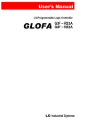
1
User’s Manual
LG Programmable Logic Controller
G3F-AD4A
G3F-AD4B
G4F-AD2A
LG Industrial Systems
SAFETY PRECAUTIONS
Be sure to read carefully the safety precautions given in data sheet and user’s manual before operating the module
and follow them.
The precautions explained here only apply to the G3F-AD4A , G3F-AD4B and G4F-AD2A.
For safety precautions on the PLC system, see the GLOFA GM3/4 CPU User’s Manuals and MASTERK200S/300S/1000S CPU User’s Manuals.
A precaution is given with a hazard alert triangular symbol to call your attention, and precautions are represented
as follows according to the degree of hazard.
!
WARNING
If not provided with proper prevention, it can cause death or fatal
injury or considerable loss of property.
!
CAUTION
If not properly observed, it can cause a hazard situation to result
in severe or slight injury or a loss of property.
However, a precaution followed with
!
can also result in serious conditions.
CAUTION
Both of two symbols indicate that an important content is mentioned, therefore, be sure to observe it.
Keep this manual handy for your quick reference in necessary.
Design Precautions
!
CAUTION
▶ Do not run I/O signal lines near to
high voltage line or power line.
Separate them as 100 mm or
more as possible. Otherwise,
noise can cause module malfunction.
Installation Precautions
!
CAUTION
▶ Operate the PLC in the environment conditions given in the
general specifications.
▶ If operated in other environment
not specified in the general
specifications, it can cause an
electric shock, a fire, malfunction
or damage or degradation of the
module
▶ Make sure the module fixing projections is inserted into the module fixing hole and fixed.
▶ Improper installation of the module can cause malfunction, disorder or falling.
Wiring Precautions
!
CAUTION
▶ When grounding a FG terminal, be sure to provide class 3 grounding which is dedicated to
the PLC.
▶ Before the PLC wiring, be sure to check the rated voltage and terminal arrangement for
the module and observe them correctly.
If a different power, not of the rated voltage, is applied or wrong wiring is provided, it can
cause a fire or disorder of the nodule.
▶ Drive the terminal screws firmly to the defined torque.
If loosely driven, it can cause short circuit, a fire or malfunction.
▶ Be careful that any foreign matter like wire scraps should not enter into the module.
It can cause a fire, disorder or malfunction.
Test Run and Maintenance
Precautions
!
!
WARNING
▶ Do not contact the terminals
while the power is applied.
It can cause malfunction.
▶ When cleaning or driving a terminal screw, perform them after the
power has been turned off
▶ Do not perform works while the
power is applied, which can
cause disorder or malfunction.
CAUTION
▶ Do not separate the module from
the printed circuit board(PCB), or
do not remodel the module.
They can cause disorder, malfunction, damage of the module
or a fire.
When mounting or dismounting
the module, perform them after
the power has been turned off.
▶ Do not perform works while the
power is applied, which can
cause disorder or malfunction.
Waste Disposal Precautions
!
CAUTION
▶ When disposing the module, do it as an industrial waste.
◎ CONTENTS ◎
Chapter 1. INTRODUCTION
1.1 Features ·································································································································································1-1
1.1.1 G3F -AD4A /G3F-AD4B ··································································· 1-1
1.1.2 G4F -AD2A ············································································ 1-1
1.2 Glossary·································································································································································1-2
1.2.1 A -A nalog Value ········································································ 1-2
1.2.2
D-D igitalValue ········································································· 1-2
1.2.3 Analog / DigitalC onversion C haracteristics ·················································· 1-3
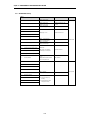
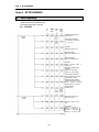
Chapter 2. SPECIFICATIONS
2.1 General Specifications ··································································································································2-1
2.2
Performance Specifications ·······················································································································2-2
2.3 Names of Parts and Functions ··················································································································2-3
2.3.1 G3F -AD4A ············································································ 2-3
2.3.2
G4F-AD2A ············································································ 2-5
2.3.3
G3F-AD4B ············································································ 2-6
2.4 I/O Conversion Characteristics ·················································································································2-7
2.4.1
G3F-AD4A I/OC haracteristics
··························································· 2-8
1) Voltage Input C haracteristics ······························································ 2-9
2) Current Input C haracteristics ····························································· 2-10
3) Simultaneous Voltage and C urrent Input C haracteristics ········································2-11
2.4.2
G4F-AD2A I/OC haracteristics ··························································· 2-12
1) Voltage Input C haracteristics ····························································· 2-12
2) Current Input C haracteristics······························································ 2-14
3) Simultaneous Voltage and C urrent Input C haracteristics ······································· 2-15
2.4.3
G 3F-AD4B I/OC haracteristics ··························································· 2-16
1) Voltage Input C haracteristics ····························································· 2-17
2) Current Input C haracteristics······························································ 2-17
3) Simultaneous Voltage and C urrent Input C haracteristics ······································· 2-18
4) The connection between Analog input and Digital output ······································· 2-18
2.4.4
The connection between O ffset/ G ain S etting and Digital O utput Value ··························· 2-19
1) Resolution ··········································································· 2-19
2) Relations between M axim u m R esolution and Digital O utput Value ······························· 2-19
3) O ffset/ G ain S etting ··································································· 2-20
(1) O ffset/ G ain Setting of the G3F -AD4A ················································· 2-20
(2) O ffset/ G ain Setting of the G4F -AD2A ·················································· 2-22
2.5 A/D Conversion Characteristics ················································································································2-24
2.5.1 FilterP rocessing ······································································ 2-24
2.5.2 S ampling Processing (Instantaneous Value) ················································ 2-25
2.5.3 Average Processing ··································································· 2-25
Chapter 3. INSTALLATION AND WIRING
3.1
Installation ··························································································································································3-1
3.1.1 Installation A m b ience ···································································· 3-1
3.1.2 Handling Precautions ··································································· 3-1
3.2 Wiring ···································································································································································3-2
3.2.1
W iring Precautions ····································································· 3-2
3.2.2
W iring Examples ······································································· 3-2
1) G3F-AD4A ············································································ 3-2
2) G4F-AD2A ············································································ 3-3
3) G3F-AD4B ············································································ 3-4
Chapter 4. FUNCTION BLOCK
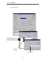
4.1 Insertion of the Function Block for the A/D Conversion Module on the GMWIN ················4-1
4.2 Local Function Block ·····································································································································4-2
4.2.1 Module Initializ ation(G3F-AD4A: AD4IN I,G4F -AD2A: AD2IN I, G3F-AD4B: AD4BINI) ················ 4-2
4.2.2 Module Reading -A rray Type (G3F -AD4A:AD4ARD, G4F -AD2A:AD2ARD,G3F-AD4B:AD4BARD) ····· 4-3
4.2.3 Module Reading -S ingle Type (G3F-AD4A:AD4RD,G4F-AD2A:AD2RD, G3F-AD4B:AD4BRD) ········ 4-3
4.3
Remote Function Block ································································································································4-4
4.3.1 Module Initialization (G3F-AD4A: AD4RINI, G4F -AD2A: ADR2INI, G3F -AD4B: ADR4BIN I) ············ 4-4
4.3.2 Module Reading (G3F-AD4A: ADR4RD, G4F-AD2A: ADR2RD, G3F-AD4B: ADR4BRD ) ·············· 4-5
4.4
Errors on Function Block ····························································································································4-6
Chapter 5. GM PROGRAMMING
5.1 Programming for Distinction of A/D Conversion Value ····································································5-1
5.2 Programming for Display of A/D Conversion Value and Error Code on BCD Display ········5-7
5.3 Programming for Loading the A/D Conversion Module on Remote I/O Station ················5-10
Chapter 6. BUFFER MEMORY CONFIGURATION AND FUNCTION
6.1 Buffer Memory Configuration ····················································································································6-1
6.1.1
G3F -AD4A ············································································ 6-1
6.1.2 G 3F-AD4B ············································································ 6-2
6.1.3
G4F -A D2A ············································································· 6-4
6.2 Buffer Memory Functions·······························································································································6-5
6.2.1 Available C hannel S pecificationA rea ······················································· 6-5
6.2.2 Input Used Type Specification Area ························································· 6-5
6.2.3
Data O utput Type SpecificationArea ······················································· 6-6
6.2.4 Filter P rocessing Enable/D isable S pecificationArea ··········································· 6-6
6.2.5 Filter C onstant S etting A rea ······························································ 6-7
6.2.6 Average Processing Enable/D isable S pecificationArea ········································ 6-8
6.2.7 Number /Time Average Processing Area ···················································· 6-9
6.2.8 Average N umber/Time C onstant S etting Area ··············································· 6-10
6.2.9 SET Data Specification Area ···························································· 6-10
6.2.10
Digital Value O utput Area ·······························································6-11
6.2.11
ChannelO peration Data S torage Area ·····················································6-11
6.2.12
E rrorC ode D isplay Area ································································6-11
Chapter 7. SPECIAL MODULE COMMAND (Buffer Memory READ / WRITE)
7.1 Local Command ···············································································································································7-1
7.1.1 Internal M emory Read -GET, GETP ························································ 7-1
7.1.2 Internal memory W rite -PUT, PUTP ························································· 7-2
7.2 Remote Command ··········································································································································7-3
7.2.1
BufferM emory R ead –R G E T ····························································· 7-3
7.2.2
BufferM emory W rite –R P U T ····························································· 7-4
Chapter 8. MK PROGRAMMING
8.1 Basic Programming ········································································································································8-1
8.1.1 G3F -AD4A ············································································ 8-1
8.1.2 G4F -AD2A ············································································ 8-2
8.2 Application Programming ···························································································································8-3
8.2.1 P rogramming for Distinction of A/DC onversion Value ·········································· 8-3
8.2.2 P rogramming for Display of A/DC onversion Value and Error C ode on BCD D isplay ·················· 8-5
8.2.3 Programming for Loadin g the A/DC onversion M odule on Remote I/O S tation ······················· 8-7
Chapter 9. TROUBLESHOOTING
9.1
Error Code ··························································································································································9-1
9.1.1 E rrorC ode Indicated by RUN LED Flickering ················································ 9-1
9.2
Troubleshooting ·················································································································································9-2
9.2.1
RUN LED Flickering ···································································· 9-2
9.2.2
RUN LED O ff ·········································································· 9-2
9.2.3
Digital Value U nreadable from the CPU Module ·············································· 9-3
9.2.4 Sudden DigitalValue C hange ····························································· 9-3
9.2.5 Analog and Digital Value M ism a tch························································· 9-4
9.2.6 A/D C onversion M odule H ardware Fault ···················································· 9-4
Chapter 10. DIMENSIONS
10.1 G3F-AD4A , G3F-AD4B Dimensions ····································································································10-1
10.2 G4F-AD2A Dimensions ·····························································································································10-2
Chapter 1. INTRODUCTION
Chapter 1. INTRODUCTION
The G4F-AD2A, G3F-AD4A and G3F-AD4B are analog/digital conversion modules for use with the GLOFA PLC GM 1/2/3/4
series CPU module and the MASTER-K PLC K300S/1000S Series CPU module. The G4F-AD2A is used on GM4 series
module and the K300S series module, and the G3F-AD4A and G3F -AD4B is used on the GM1/2/3 series module and the
K1000S series module. (Hereafter the G4F-AD2A, G3F-AD4A and G3F-AD4B are called the A/D conversion module) The
A/D conversion module is to convert an analog input signal (voltage or current) from external sensors into a 14-bit binary
digital value.
1.1 Features
1.1.1
G3F-AD4A / G3F-AD4B
1) 16-Channel analog to digital conversion is possible with a single module.
The G3F-AD4A and G3F-AD4B hav e 16-Channel A/D conversion capacity, with each channel selectable for
voltage or current input.
2) High resolution of 1/16000
High-resolution digital values can be obtained. Resolution setting applies to all channels.
4) The number of the G3F-AD4A used on one base is unlimited.
1.1.2
G4F-AD2A
1) 4-Channel analog to digital conversion is possible with a single module.
The G3F-AD2A has 4-Channel A/D conversion capacity, with each channel selectable for voltage or current
input.
2) High resolution of 1/16000
High-resolution digital values can be obtained. Resolution setting applies to all channels.
3) The number of the G4F-AD2A used on one base is unlimited.
1 -1
Chapter 1. INTRODUCTION
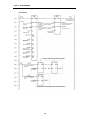
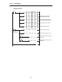
1.2 Glossary
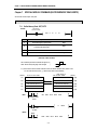
Transducer
[ Fig 1.1] Analog Value
1.2.1
[Fig 1.2]
Transducer
A-Analog Value
Analog value is a sequentially changing value such as voltage, current, temperature, speed, pressure, flux, etc.
Temperature, for example, is sequentially changing according to the time. Because this temperature is not input
on the PLC through transducer, the same analog value of DC voltage (0 to ± 10 V) or current (4 to 20 mA) in
accordance with the temperature should be inputted on the PLC.
1.2.2
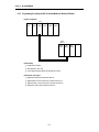
D-Digital Value
Digital value is non-sequentially changing value written as the number like 0,
1, 2, 3. The signal of on or off is written as digital value of 0 or 1.
There are BCD value and binary value in the range of digital value.
Time
[Fig 1.3] Digital Value
Analog value isn't written directly onto the CPU. For analog input to the
CPU operation, analog converted to digital value has to be inputted onto
the CPU and for analog output, the digital value of the CPU should be
converted to analog value.
Analog input
0 to ± 10 V or
0 to ± 20 mA
Analog output
0 to ± 10 V or
0 to ± 20 mA
[Fig 1.4] PLC Processing
1 -2
Chapter 1. INTRODUCTION
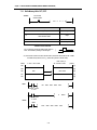
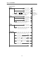
1.2.3 Analog/ Digital Conversion Characteristics
1) Voltage input
Input
InputVoltage
Voltage
[Fig 1.5] A/D Conversion Characteristics (Voltage Input)
Analog/digital conversion module allows external analog input to be converted to digital value and to be operated
in the CPU. On voltage input, input of –10 V leads to digital value of 0 and 10 V to 16000.
Input of 1.25 mV is equal to digital value of 1. Therefore, input less than 1.25 mV shouldn't be converted but
ignored.
2) Current input
Analog input current
Current
input
Input
Current
[Fig 1.6] A/D Conversion Characteristics (Current input)
On current input, input of -20 mA leads to digital value of 8000 and 20 mA to 16000. Input of 2.5㎂ is equal to
digital value of 1. Therefore, input less than 2.5㎂ shouldn't be converted but ignored.
1 -3
Chapter 2. SPECIFICATIONS
Chapter 2 . SPECIFICATIONS
2.1
General Specifications
Table 2.1 shows the general specifications of GLOFA GM series and MASTER-K series.
No
1
2
3
4
Item
Operating ambient
temperature
Storage ambient
temperature
Operating ambient
humidity
Storage ambient
humidity
5
Vibration
6
Shocks
7
Specifications
Standard
0 ~ 55℃
-25 ~ 70℃
5 ~ 95%RH, non-condensing
5 ~ 95%RH,
non-condensing
Occasional vibration
Acceleration
Amplitude
Sweep count
0.075 mm
9.8㎨ {1G}
10 times in each
Continuos vibration
direction for
Frequency
Acceleration
Amplitude
X, Y, Z
0.035 mm
10≤f∠57 Hz
57≤f≤150 Hz 4.9㎨{0.5G}
*Maximum shock acceleration: 147㎨ {15G}
*Duration time :11 ms
*Pulse wave: half sine wave pulse( 3 times in each of X, Y and Z directions )
Frequency
10≤f∠57 Hz
57 ≤f≤150 Hz
Square wave impulse noise
±1,500 V
Electrostatic discharge
Voltage :4kV(contact discharge)
Radiated electromagnetic field
27 ~ 500 MHz, 10 V/m
Noise immunity
Severity
Level
Fast transient burst noise
Digital I/Os
Digital
I/Os
(Ue < 24 V)
All power
( Ue
Analog I/Os
modules
communication
≥
24 V)
I/Os
Voltage
8 Operating atmosphere
2 kV
1 kV
IEC 61131-2
IEC 61131-2
IEC 61131-2
IEC 1000-4-2
IEC 61131-2
IEC 1000-4-3
IEC 61131-2
IEC 1000-4-4
0.25 kV
Free from corrosive gases and excessive dust
9
Altitude for use
Up to 2,000m
10
Pollution degree
2 or lower
11
Cooling method
Self-cooling
[Table 2.1 ] General specifications
REMARK
1) IEC(International Electrotechnical Commission)
: The international civilian organization which produces standards for electrical and electronics industry.
2) Pollution degree
: It indicates a standard of operating ambient pollution level.
The pollution degree 2 means the condition in which normally, only non-conductive pollution occurs.
Occasionally, however, a temporary conductivity caused by condensation shall be expected.
2-1
Chapter 2. SPECIFICATIONS
2.2
Performance Specifications
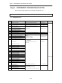
Table 2-2 shows performance specifications of A/D conversion module.
Specifications
Items
G3F-AD4A
G4F-AD2A
I/O points
Analog input
16 points
Voltage
–5 ~ 5 VDC (input resistance 560㏀)
–10 ~ 10 VDC (input resistance 560㏀)
1 ~ 5 VDC
(input resistance 560㏀)
Current
DC –20 ~ 20 mA (input resistance 250Ω)
4 ~ 20 mA
(input resistance 250Ω)
*. Select with the Input conversion
*. Select in accordance with the
switch on the side of the module
Input terminals.
(on: current, off: voltage)
*. Connect the V terminal with the
*. Select with program initial F/B
I terminal on the use of
(input variable:IN_SEL, 0:current,
current input.
1:voltage)
*. Select with the Input conversion
switch on the side of the module
Voltage/Current
(on: current, off: voltage)
selection
*. When current input is used, set the
Input range switch to V1 / I.
*. 16-bit (data: 14bit)signed binary
*. May be set per channel by setting output data
("0": -192 to 16191, "1": -8192 to 8191)
Digital output
Maximum
resolution
G3F-AD4B
*. 16-bit (data: 14bit)signed binary
("0": 0 to 16000, "1": -8000
to 8000)
1 ~ 5 VDC
-
0.25 mV (1/16000)
-5 ~ 5 VDC
0.625 mV (1/16000)
-
-10 ~ 10 VDC
1.25 mV (1/16000)
-
DC 4 ~20 mA
-
1.0 ㎂ (1/16000)
DC -20 ~20 mA
0.0025 mA (1/16000)
-
±0.5% or lower
Overall Accuracy(%)
(accuracy to full scale)
(accuracy to full scale)
(±0.3% at ambient temperature 25℃)
Maximum conversion speed
(ms/channel)
3.0
(accuracy to full scale)
(±0.3% at ambient temperature 25℃
5.0
Voltage(V):±12,
Maximum absolute input
Number of analog input point
±0.5% or lower
±0.2% or lower
16 channels/module
3.0
Current (mA):±25
4 channels/module
16 channels/module
Between input terminals and PLC: Photo coupler isolation
(Between channels : Non-isolated)
Isolation
Terminals connected
38-point terminal block
20-point terminal block
38-point terminal block
Internal current
consumption(A)
Weight (g)
0.67 A
0.4 A
0.54 A
630
360
560
[Table 2.2] Performance Specifications
! CAUTION
The offset / gain value of G3F-AD4B A/D conversion module at factory has been fixed. Therfore it is not
Changed.
2-2
Chapter 2. SPECIFICATIONS
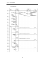
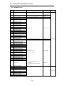
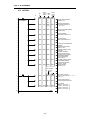
2.3
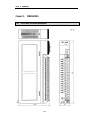
Names of Parts and Functions
The names of parts and functions of the A/D conversion module are shown as below.
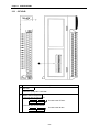
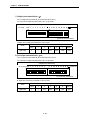
2.3.1 G3F-AD4A
The names of parts and functions of the A/D conversion module are shown
②
③
④
⑤
2-3
Chapter 2. SPECIFICATIONS
No
①
Descriptions
RUN LED
Indicates the operating status of the G3F-AD4A
(1) On
: Normal operation
(2) Flicker : An error has occurred. (For more information, see the General Section 4.1)
(3) Off
: DC 5 V power-off or G3F-AD4A module fault.
② Offset Trimmer
③
Used to make micro adjustment of an offset value.
Gain Trimmer
④
Used to make micro adjustment of a gain value.
Input range switch
- On factory set, the voltage range has to be set to from -10 to 10 VDC.
(1) Set to voltage
V1 : Voltage range -5 ~ 5 VDC
V2 : Voltage range -10 ~ 10 VDC
(2) Set to current
I : Current range -20 ~ 20 mA
: Unusable
⑤
Input select switch
(1) Used to select the analog input(voltage or current input) of each channel
-Set to OFF to use voltage input.
-Set to ON to uses current input.
(2) On factory set, it has to be set to voltage input condition. (Every Dip Switch is off.)
2-4
Chapter 2. SPECIFICATIONS
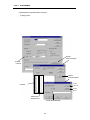
2.3.2 G4F-AD2A
This section shows the names of parts and functions of G4F-AD2A module.
No
Descriptions
No
Descriptions
← RUN LED
↓ GAIN switch
Indicates the operating status of the G4F-AD2A.
Adjust upward, and the analog input value of
Normal mode: channel switch's setting range: 4 to F
corresponding channels is stored as a gain value.
- ON : Normal operation.
° Input range select switch
- Flicker : An error has occurred.
- OFF : DC5V power-off or G3F-AD4A module fault.
Switch
Analog input
Test mode: channel switch's range: 0 to 3
- Flicker(per 1.0sec) : No operation of offset/gain switch.
-10 ~ 10 VDC
- ON
: Offset/gain switch adjusted upward.
Voltage
- Flicker(per 0.2sec) : offset/gain setting error.
-5 ~ 5 VDC
↑ Offset switch
Adjust upward, and the analog input value of corresponding
channels is stored as an offset value.
→
Channel switch for the test mode
Corresponding channels will be selected in the adjustment of
offset/gain value. (Valid range: 0 to 3 )
2-5
Current
-20 ~ 20 mA
* Don’t put the input switch on
* It leads to malfunction.
or
Chapter 2. SPECIFICATIONS
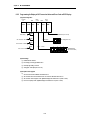
2.3.3 G3F-AD4B
G3F-AD4B
②
1~5V
4~20mA
Description
← RUN LED
Indicates the operating status of G3F-AD4B
↑
Selection switch of voltage/current
1) The switch status at voltage selection
On
12345678
On
The switch locates OFF status.
12345678
2) The switch status at current selection
On
12345678
On
The switch locates ON status.
12345678
2-6
Chapter 2. SPECIFICATIONS
2.4
I/O Conversion Characteristics
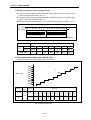
Input / Output (hereafter I/O) conversion characteristics are expressed by the angle of the line connecting the
offset value and gain value used to convert the analog signals, input to the PLC into digital values.
The I/O conversion characteristics of the A/D conversion module are shown as below.
G3F-AD4A
Practical analog input range
Gain value
Digital
Output
Value
Offset value
Range: - 10 ~ 10 VDC
Range: - 5 ~ 5 VDC
Range: - 20 ~ 20 mA
Analog Input
G4F-AD2A
Practical analog input range
Gain value
Digital
Output
Value
Offset value
Range: - 10 ~ 10 VDC
Range: - 5 ~ 5 VDC
Range: - 20 ~ 20 mA
Analog Input
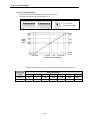
[Fig 2.1] I/O Conversion Characteristics
2-7
Chapter 2. SPECIFICATIONS
2.4.1 G3F-AD4A I/O Characteristics
The G3F-AD4A allows voltage or current input to be selected per channel by the input select switch.
Offset / gain setting is performed for 16 channels in block.
1) Voltage Input Characteristics
For voltage input, the input select switch of each channel is set to "off".
Position of Input select switch
- Off : Voltage
(On the left side of the Module)
Channel number
a) Range : -10 ~ 10 VDC
-The analog input range switch has to be set to downward (V2).
Position of Analog input range switch
V1/ I (–5~5 VDC select)
V2 (–10~10 VDC select)
<On the front side of the module>
Digital
Output
Value
0V 1V
-10.24 V -10 V
5V
10 V 10.24 V
Analog Input (Voltage)
Analog input (voltage)
-The digital output value according to voltage input characteristics will be shown as below.
Analog input voltage
Digital output
range
-10.24V
-10 V
0V
1V
5V
10V
10.24V
-192~16191
-192
0
8000
8800
12000
16000
16191
-8192~8191
-8192
-8000
0
800
4000
8000
8191
2-8
Chapter 2. SPECIFICATIONS
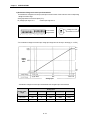
b) Range: -5 ~ 5 VDC
-The analog input range switch has to be set upward (V1/ I)
The way to set analog input range switch
V1/ I (–5~5 VDC select)
V2 (–10~10 VDC select)
<The front side of the module>
Digital
Output
Value
-5.12 V –5 V
0V 1V
3V
5 V 5.12 V
Analog Input Value (Voltage)
-The digital output value according to voltage input characteristics will be shown as below.
Analog input voltage
Digital output
range
-5.12 V
-5 V
0V
1V
3V
5V
5.12 V
-192~16191
-192
0
8000
9600
12800
16000
16191
-8192~8191
-8192
-8000
0
1600
4800
8000
8191
2-9
Chapter 2. SPECIFICATIONS
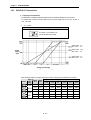
2) Current Input Characteristics
- For current input, the input select switch of each channel is set to "on".
Analog input range switch has to be set upward (V1/ I).
Input select switch position
Analog input range switch position
V1/ I (DC –20~20mA)
V2 (Current input disable)
Digital
Output
Value
9600
-20.48 m-20mA
0mA 4mA
12mA
20mA 20.48mA
Analog Input Value (Voltage)
-
The digital output value according to current input characteristics will be shown as below.
Analog input current
Digital output
range
-20.48 mA
-20 mA
0 mA
4 mA
12
20
20.48 mA
-192~16191
-192
0
8000
9600
12800
16000
16191
-8192~8191
-8192
-8000
0
1600
4800
8000
8191
2 - 10
Chapter 2. SPECIFICATIONS
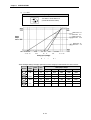
3) Simultaneous Voltage and Current Input Characteristics
For simultaneous voltage and current input, the input conversion switch of each channel is set to corresponding
voltage and current range.
Analog input switch has to be set upward (V1/ I).
Ex) Voltage input range: 0 to 7
Current input range: 8 to 15
Input select switch position
Analog input range switch position
V1/ I Voltage:-5~5 VDC
Current selection
Voltage selection
V2
Current:DC-20~20 mA
- For simultaneous voltage and current input, voltage input range has to be set only to the range [-5 ~ 5 VDC].
8191
8000
Digital
Output
Value
0
-8000
-8191
Analog Input
- Simultaneous voltage and current input characteristics lead to digital output value as below.
Analog input
Digital output
range
-5.12 V
-5 V
0V
5V
5.12 V
-20.48 mA
-20 mA
0 mA
20 mA
20.48 mA
-192~16191
-192
0
8000
16000
16191
-8192~8191
-8192
-8000
0
8000
8191
2 - 11
Chapter 2. SPECIFICATIONS
2.4.2 G4F-AD2A I/O Characteristics
1) Voltage Input Characteristics
- The G4F-AD2A is capable of selecting voltage/current and adjusting offset/gain for each channel.
- For voltage input, the input conversion switch may be set to the range such as from-10 to 10 VDC, or
from -5 to 5 VDC.
a) -10 ~ 10 VDC
Position of input range switch
Turn switch 1 on and switch 2 off.
(On the left side of the module)
Offset value : -5 V
Gain value :0 V
Offset value : -10V
Gain value :0 V
Digital
Output
Value
Offset value : 0V
Gain value :5 V
-10.24 V –10 V
-5 V
0V
5V
10 V 10.24 V
Analog Input (Voltage)
- When offset/gain setting is changed, digital output value to voltage input characteristics are as below.
Section
Ex 1
Ex 2
Ex 3
Ex 1
Ex 2
Ex 3
Digital
output
range
Offset
value
Gain
value
- 10 V
-5V
0V
3V
5V
10 V
-192
~
16191
-5 V
0V
-192
0
8000
12800
16000
16191
-10 V
0V
0
4000
8000
10400
12000
16000
0V
5V
-192
-192
0
4800
8000
16000
-5 V
0V
-8192
-8000
0
4800
8000
8191
-10 V
0V
0
-4000
0
2400
4000
8000
0V
5V
-8192
-8192
-8000
-3200
0
8000
-8192
~
8191
Analog input voltage
2 - 12
Chapter 2. SPECIFICATIONS
b) -5 ~ 5 VDC
Position of input range switch
Turn switch 1 off and switch 2 on.
(On the left side of the module)
Offset value : -5 V
Gain value : 0 V
Digital
Output
Value
Offset value : 0V
Gain value : 2.5 V
Offset value : 1V
Gain value : 3 V
-5.12 V –5 V
-2.5 V
0V 1V
2.5 V
5 V 5.12 V
Analog Input (Voltage)
- When offset/gain setting is changed, digital output value to voltage input characteristics are shown as below.
Section
Ex 1
Ex 2
Ex 3
Ex 1
Ex 2
Ex 3
Digital
output
range
Offset
value
Gain
value
-5V
0V
1V
3V
5V
-192
~
16191
-5 V
0V
0
8000
9600
12800
16000
0V
2.5 V
-192
0
3200
9600
16000
1V
3V
-192
-192
0
8000
16000
-8192
~
8191
-5 V
0V
-8000
0
1600
4800
8000
0V
2.5 V
-8192
-8000
-4800
1600
8000
1V
3V
-8192
-8192
-8000
0
8000
Analog input voltage
2 - 13
Chapter 2. SPECIFICATIONS
2) Current Input Characteristics
Offset value : -20 mA
Gain value :0 mA
Ex3 Offset value:4mA
Offset
value : 0mA
Gain
value:12mA
Digital
Output
Value
Gain value :10mA
Offset value : 4mA
Gain value :12mA
-20mA
0mA
4mA 10mA 12mA
20mA
Analog Input (Current)
- When offset/gain setting is changed, digital output value to current input characteristics are shown as below.
Section
Ex 1
Ex 2
Ex 3
Ex 1
Ex 2
Ex 3
Digital
output
range
Offset
value
Gain
value
- 20 mA
0 mA
4 mA
10 mA
12 mA
20 mA
-192
~
16191
-20 mA
0 mA
0
8000
9600
12000
12800
16000
0 mA
10 mA
-192
0
3200
8000
9600
16000
4 mA
12 mA
-192
-192
0
6000
8000
16000
-8192
~
8191
-20 mA
0 mA
-8000
0
1600
4000
4800
8000
0 mA
10 mA
-8192
-8000
-4800
0
1600
8000
4 mA
12 mA
-8192
-8192
-8000
-2000
0
8000
Analog input current
2 - 14
Chapter 2. SPECIFICATIONS
3)
Simultaneous Voltage and Current Input Characteristics
-When voltage and current are input simultaneously, the input range switch of the left side of the module has
to be set to the range from -5 to 5 VDC. (Switch 1 turns Off, Switch 2 turns On )
Ex) Voltage input channel : 0,
Current input channel : 1
Input range select switch
(on the left side of module)
Terminal connection
voltage input (channel 0)
current input (channel 1)
-5 ~ 5 VDC
-10 ~ 10 VDC
-When voltage and current are input simultaneously, voltage input range has to be set only to the range from
-5 to 5 VDC.
Digital
Output
Value
Analog Input
2 - 15
Chapter 2. SPECIFICATIONS
-When offset/gain setting is changed, digital output value to voltage/current input characteristics are shown
as below.
Section
Ex 1
Ex 2
Ex 3
Ex 1
Ex 2
Ex 3
Digital
output
range
Offset value
(Voltage
/ Current)
Gain value
(Voltage
/ Current)
-192
~
16191
-5 V / -20 mA
-8192
~
8191
Analog input
-5 V
0V
1V
2.5 V
3V
5V
- 20 mA
0 mA
4 mA
10 mA
12 mA
20 mA
0 V / 0 mA
0
8000
9600
12000
12800
16000
0 V / 0 mA
2.5 V / 10 mA
-192
0
3200
8000
9600
16000
1V / 4 mA
3 V / 12 mA
-192
-192
0
6000
8000
16000
-5 V / -20 mA
0 V / 0 mA
-8000
0
1600
4000
4800
8000
0 V / 0 mA
2.5 V / 10 mA
-8192
-8000
-4800
0
1600
8000
1 V / 4 mA
3 V / 12 mA
-8192
-8192
-8000
-2000
0
8000
! Caution
1. When digital output is set to the range of -192 to 16191, despite a analog input more than the range of -192 to
16191, Digital output value is set to-192 or 16191.
When digital output is set to the range of –8192 to 8191, despite a analog input more than the range of -8192
or 8191, digital output value is set to -8192 or 8191.
2. Do not apply ±15 V /±25 mA or more. This will damage the module due to a heat rise.
3. Set an offset/gain value on the G4F-AD2A to the range that gain value is more than offset value, or you won't
get an accurate digital output.
2 - 16
Chapter 2. SPECIFICATIONS
2.4.3 G3F-AD4B I/O Characteristics
▶ I/O conversion characteristics are expressed by the angle of used to convert the analog signals(voltage or
current input), input to the PLC into digital values as shown below
▶ A/D coversion module is possible to select voltage/current by analog input range select switch by channel but cannot change
offset/gain value because it is set
Practical analog input range
16000
12000
Digital
output
8000
4000
0
Analog
input
DC 4 ~ 20 ㎃
DC 1 ~ 5V
3.808 ㎃
0.952V
4㎃
12 ㎃
3V
1V
20 ㎃
20.192 ㎃
5V
5.048V
I/O Conversion characteristics
!
Caution
1. Despite a analog input more than the range of 16000 or 0, digital output value is set to 16000 or 0.
2. Do not apply +15 V /+25 mA or more. This will damage the module due to a heat rise.
2 - 17
Chapter 2. SPECIFICATIONS
1) Voltage input characteristics(DC 1 ~5V)
▶ For voltage input, input variables IN_SEL of initial funtion block is set to “1”
▶ The position of voltage/current select switch is set to “off” by channel
Voltage/Current select switch
CH0
-.Off : Voltage
1
2
3
4
5
6
7
On
8
9 10 11
12 13 14 15
Channel no.
On
1 2 3 4 5 6 7 8
1 2
3
4
5
6
7
8
(On the left side of the Module)
▶Digital value to voltage input characteristics is shown as below
Analog input voltage(V)
Section
Lower 1
1
2
3
4
5
Upper 5
0
0
4000
8000
12000
16000
16000
Digital output
2) Current input characteristics(DC 4 ~20mA)
▶ For current input, input variables IN_SEL of initial funtion block is set to “0”
▶ The position of voltage/current select switch is set to “on” by channel
Voltage/Current select switch
- On : Current CH0
1
2
3
4
5
6
7
On
8
9
10 11 12 13 14 15
2
3
Channel no.
On
1
1 2 3 4 5 6 7 8
4 5
6
7
8
(On the left side of the Module)
▶ Digital value to current input characteristics is shown as below
Section
Digital output
Analog input current(㎃)
Lower 4
4
8
12
16
20
Upper 20
0
0
4000
8000
12000
16000
16000
2 - 18
Chapter 2. SPECIFICATIONS
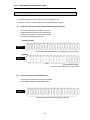
3) Simultaneous Voltage and Current Input Characteristics
▶ For the channel used to voltage input, input variable IN_SEL of initial funtion block is set to “1” by channel, and the
position of voltage/current select switch is set to “off”
▶ For the channel used to current input, input variable IN_SEL of initial funtion block is set to “0” by channel, and the
position of voltage/current select switch is set to “on”
Ex) The channel used to voltage input : channel 0~3, 8~11, The channel used to current input : channel 4~7,12~15
Voltage/Current select switch
- On : current CH0
- Off : voltage
On
1
2
3
4
5
6
8
7
9 10 11 12 13 14 15
Channel no.
On
1
1 2 3 4 5 6 7 8
2
3
4
5
6
7 8
(On the left side of the Module)
▶Digital output to voltage/current input characteristics is shown as below
Section
Input
type
Analog input
1~ 5V
Lower 1
1
2
3
4
5
Upper 5
4~20㎃
Lower 4
4
8
12
16
20
Upper 20
0
0
4000
8000
12000
16000
16000
Digital output
4) The connection between Analog input and Digital output
The connection between Analog input and Digital output is shown as below
8009
8008
8007
8006
8005
8004
8003
8002
8001
8000
Digital output
Input range
DC 1~5V
DC 4~20
㎃
Digital
output
0~
16000
①
Resolution
Analog input
0.25mV
3.000
~
3.00025
3.00025
~
3.00050
3.00050
~
3.00075
3.00075
~
3.00100
3.00100
~
3.00125
3.00125
~
3.00150
3.00150
~
3.00175
3.00175
~
3.00200
3.00200
~
3.00250
3.00250
~
3.00275
1㎂
12.000
~
12.001
12.001
~
12.002
12.002
~
12.003
12.003
~
12.004
12.004
~
12.005
12.005
~
12.006
12.006
~
12.007
12.007
~
12.008
12.008
~
12.009
12.009
~
12.010
Analog input and Digital output
2 - 19
Chapter 2. SPECIFICATIONS
2.4.4
The connection between Offset/Gain Setting and Digital Output Value
1) Resolution
Resolution is determined as below formulas.
(1) Voltage input
Resolution =
Gain value - Offset value
8000
Ex) Gain value : 0 V
Resolution =
(2) Current input
Resolution =
1000 (mV)
Offset value : - 10 V
0 – ( - 10 )
8000
5 1000 mV = 1.25 mV
Gain value - Offset value
8000
Ex) Gain value : 0 mA
Resolution =
5
0 – ( - 20 )
8000
5
1000 (µA)
Offset value : - 20 mA
5 1000 µA = 2.5 µA
2) The connection between Maximum Resolution and Digital Output Value
On the occasion of calculating, as follows, by offset/gain setting, digital output value 1 at a time doesn't
increase or decrease.
Gain value - Offset value
8000
< Resolution
2 - 20
Chapter 2. SPECIFICATIONS
3)
Offset / Gain Setting
(1) Offset/gain setting of the G3F-AD4A
a) Offset/gain sets procedure.
: Offset/gain setting is performed for 16 channels in block.
Setting input range switch and input select switch
Write a program for the A/D conversion into the memory
of the CPU module, and operate the CPU module.
Select input range
After making programs of
used channel, operate the
CPU module
Apply offset voltage (or current) to input terminal of channel 0.
Offset micro adjustment
Adjust the offset trimmer until the digital value on the LED
display corresponds to the offset value.
Apply gain voltage (or current) to input terminal of channel 0.
Gain micro adjustment
Adjust the gain trimmer until the digital value on the LED
display corresponds to the gain value.
Offset/gain micro adjustment has been completed
2 - 21
Chapter 2. SPECIFICATIONS
b) I/O characteristics in accordance with Offset/Gain setting
Digital Output Value
No
Input
range
ℵ
DC–1
0~10V
ℑ
DC
–5~5V
Digital
output
range
-192
~
16191
-192
~
16191
Offset
value
Gain
value
Resolu
tion
0V
10V
1.25
mV
0V
5V
0.625
mV
Analog input value (V)
5.000
~
5.00125
5.000
~
5.000625
5.00625
~
5.00125
5.00125
~
5.0025
5.00125
~
5.001875
5.001875
~
5.0025
5.0025
~
5.00375
5.0025
~
5.003125
5.00375
~
5.005
5.003125
~
5.00375
5.00375
~
5.004375
5.004375
~
5.005
Voltage input and digital output value
Digital output value
No
Input
range
Digital
output
range
Offset
value
Gain
value
Resoluti
on
ℵ
DC–2
0~20
mA
-192
~
16191
0
mA
20
mA
0.0025
mA
Analog input value (mA)
10.000
~
10.0025
10.0025
~
10.0050
10.0050
~
10.0075
10.0075
~
10.0100
Current input and digital output value
2 - 22
10.0100
~
10.0125
10.0125
~
10.0150
Chapter 2. SPECIFICATIONS
(2) Offset/Gain Setting of the G4F-AD2A
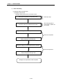
a) Offset/gain Setting Procedure
Set offset / gain values for each channel.
Set the channel select switch for test mode to channel 0.
: RUN LED flickering per 1sec
Write a program for the A/D conversion module to the memory of the
CPU module. Operate the CPU module.
Test mode
After making used
channel program,
operate the CPU module.
Apply offset voltage (or current) to input terminal of channel 0.
Offset value adjustment
Adjust the offset switch to the upward direction so that an offset value
corresponding to the channel 0 can be set.
: Adjustment of the offset trimmer upward makes RUN LED on.
Apply gain voltage (or current) to input terminal of channel 0.
Gain value adjustment
Adjust the gain switch to the upward direction so that a gain value
corresponding to the channel 0 can be set.
: Adjustment of the gain trimmer upward makes RUN LED on
Setting has completed for all used channels 0 to 3.
Offset/gain micro adjustment has completed
: Set the channel selects switch to one of channels 4 to F.
(Normal Mode state)
REMARK
(1) Set offset/gain value within practical input range.
(2) Offset/gain value is stored in the G4F-AD2A and remains after power-off.
(3) Set offset/gain value to the range of from-10 to 10 volts DC or from –20 to 20 mA.
However, if this range is exceeded, the resolution and accuracy will be impaired.
(4) At the change of grounding position in the *5 of 3.2.2, be sure to restart offset/gain value from the beginning
2 - 23
Chapter 2. SPECIFICATIONS
b) Input/output Characteristics According to Offset/Gain Setting
Digital output value
No
ℵ
ℑ
ℑ
Input
range
DC
-10~
10 V
DC
-5
~5V
DC
-5
~5V
Digital
output
range
-192
~
16191
-192
~
16191
-192
~
16191
Offset
value
Gain
value
Resolut
ion
0V
10 V
1.25
mV
0V
5V
0.625
mV
1V
2.5 V
0.125
mV
Analog input value (V)
5.000
~
5.00125
5.000
~
5.000625
5.00625
~
5.00125
5.00125
~
5.0025
5.00125
~
5.001875
5.0025
~
5.00375
5.001875
~
5.0025
4.000
~
4.000625
5.0025
~
5.003125
5.00375
~
5.005
5.003125
~
5.00375
5.00375
~
5.004375
4.000625
~
4.00125
5.004375
~
5.005
4.00125
~
4.001875
* ℜ is over the maximum resolution, so digital value 1 at a time doesn't increase or decrease.
Voltage input and digital output value
Digital output value
No
ℵ
ℑ
Input
range
DC
-20~20
mA
DC
-20~20
mA
Digital
output
range
-192
~
16191
-192
~
16191
Offset
value
Gain
value
Reso-l
ution
-20
mA
0
mA
0.0025
mA
4
mA
12
mA
0.001
mA
Analog input value (mA)
10.000
~
10.0025
10.0025
~
10.0050
16.000
~
16.0025
10.0050
~
10.0075
10.0075
~
10.0100
10.0100
~
10.0125
10.0125
~
10.0150
16.0025
~
16.0050
* ℑ is over the maximum resolution so digital value 1 at a time doesn't increase or decrease.
Current input and Digital output value
2 - 24
10.0150
~
10.0175
16.0050
~
16.0075
10.0175
~
10.0200
10.0200
~
10.0225
Chapter 2. SPECIFICATIONS
2.5
A/D Conversion Characteristics
A/D conversion
Filter processing
Sampling (instantaneous value) processing
Average processing
Number average processing
Time average processing
2.5.1 Filter Processing
Filter processing noise or the quick change of input value helps to use a stable digital value compared with
analog value.
PVfn = ( 1 - α ) × PVn + α PVfn – 1
PVfn
: present filter output value
PVn
: present A/D conversion value
PVfn-1 : previous filter output value
α
: Filter constant(the range: 0.01 to 0.99)
Filter constants used here are 1 to 99.
Ex1) G3F-AD4A/G4F-AD2A
Offset value : –10 VDC, Gain Value : 0 VDC
(Voltage input range : -10 ~ 10 VDC, Digital output range : -192 ~ 16191)
When analog value is changed in the sequence like -10V, -5V, 0V, and 5V, filter output is shown as below.
Value of α
0.01
0.5
0.99
0
0
0
Filter output value
3960
7960
11960
2000
5000
8500
40
120
239
Remarks
α leaning to the previous value by 1 %
α leaning to the previous value by 50 %
α leaning to the previous value by 99 %
Ex2) G3F-AD4B
Voltage input range : 1 ~ 5 VDC, Digital output range : 0 ~ 16000
When analog value is changed in the sequence like 1V, 2V, 3V, and 4V, filter output is shown as below.
Value of α
0.01
0.5
0.99
0
0
0
Filter output value
3960
7960
11960
2000
5000
8500
40
120
239
Remarks
α leaning to the previous value by 1 %
α leaning to the previous value by 50 %
α leaning to the previous value by 99 %
That is, filter disable allows present A/D conversion value to be displayed and filter enable allows A/D
conversion value to be displayed by filter constant according to the relative importance between present
A/D conversion value and previous value.
2 - 25
Chapter 2. SPECIFICATIONS
2.5.2 Sampling Processing (Instantaneous Value)
This is general A/D conversion processing. In other words, analog input value is to be converted to digital
value without average processing in direct. Sampling period for writing digital value to the memory is
changed according to the number of used channels.
(Process time) = (Number of channels) × Conversion speed
Ex) When 3 channels are used.
- G3F – AD4A(G3F-AD4B) : 3(number of channel used) × 3(Conversion speed) = 9 (ms)
- G4F – AD2A
: 3(number of channel used) × 5(Conversion speed) = 15 (ms)
Sampling processing means, when average processing isn't used, analog input value is to be converted to
digital value in direct.
2 - 26
Chapter 2. SPECIFICATIONS
2.5.3 Average Processing
1) The Cause of Average Processing
Average processing of noise or abnormal analog input is used to stabilize system control.
2) Kinds of Average Processing
There are kinds of average processing, which are time average and number average.
(1) Time Average Processing
a) Setting Range
G3F-AD4A(G3F-AD4B) : 96 to 12,000 (ms)
G4F-AD2A
: 40 to 20,000(ms)
b) On the time average processing, the number of average processing within the Set time is
determined according to the number of used channels .
Set time
Processing number =
Used channels×Conversion speed
Ex) Used channels : 4,
Set time : 120 ms
G3F-AD4A(G3F-AD4B) : 120÷(4×3) = 10 count
G4F-AD2A
: 120÷(4×5) = 6 count
c) When Set time divided by(Number of used channel×Conversion speed) makes the residue occur,
the processing number will be [ { average processing number ÷ ( the number of used
channel × conversion speed) } + 1] by raising the residue.
Ex) Used channels: 4,
Set time : 150 ms
G3F-AD4A(G3F-AD4B) : 150÷(4×3) = 12 count + remain 6
13 count
G4F-AD2A
8 count
: 150÷(4×5) = 7 count + remain 10
(2) Number Average Processing
a) Setting range
G3F - AD4A(G3F-AD4B, G4F-AD2A) : 2 to 4000 (count)
b) Number average processing period for writing digital value to the buffer memory is changed
according to the number of channels.
Processing time = Setting times×Number of used channels×Conversion speed
Ex) Used channels: 4, Average processing time: 50 count.
G3F - AD4A(G3F-AD4B) : 50×4×3 = 600 ms
G4F - AD2A
: 50×4×5 = 1000 ms
2 - 27
Chapter 3. INSTALLATION AND WIRING
Chapter 3.
INSTALLATION AND WIRING
3.1 Installation
3.1.1 Installation Ambience
This module has high reliability regardless of its installation ambience. But be sure to check the
following for system in higher reliability and stability.
1)
Ambience Requirements
Avoid installing this module in locations, which are subjected or exposed to:
- Water leakage and dust a large amount of dust, powder and other conductive power, oil mist,
salt, of organic solvent exists.
- Mechanical vibrations of impacts are transmitted directly to the module body.
- Direct sunlight.
- Dew condensation due to sudden temperature change.
- High or low temperatures (outside the range of 0-55℃)
2)
Installing and Wiring
- During wiring or other work, do not allow any wire scraps to enter into it.
- Install it on locations that are convenient for operation.
- Make sure that it is not located near high voltage equipment on the same panel.
- Make sure that the distance from the walls of duct and external equipment be 50 mm or more.
- Be sure to be grounded to locations that have good noise immunity.
3.1.2 Handling Precautions
From unpacking to installation, be sure to check the following:
1) Do not drop it off, and make sure that strong impacts should not be applied.
2) Do not dismount printed circuit boards from the case. It can cause malfunctions.
3) During wiring, be sure to check any foreign matter like wire scraps should not enter into the upper
side of the PLC, and in the event that foreign matter entered into it, always eliminate it.
4) Be sure to disconnect electrical power before mounting or dismounting the module.
3 -1
Chapter 3. INSTALLATION AND WIRING
3.2 Wiring
3.2.1 Wiring Precautions
1) Separate AC and external input signal of A/D conversion module wiring not to be affected by surge
or induced noise in the AC.
2) External wiring has to be at least AWG22(0.3㎟) and be selected in consideration of operating
ambience and/or allowable current.
3) Separate wiring from devices and/or substances generating intense heat, and oil not to make
short-circuit which leads to damage and/or mis-operation.
4) Identify the polarity of terminal block before external power supply is made connected.
5) Separate external wiring sufficiently from high voltage and power supply cable not to cause induced
failure and/or malfunction.
6) Don't put the power cable in front of the LED display
(In order to read the digital value on the LED correctly)
3 -2
Chapter 3. INSTALLATION AND WIRING
3.2.2 Wiring Examples
1)
G3F-AD4A
(1)
Voltage Input
Signal source –10 ~ 10 VDC
Input select switch
Input range switch
Input select switch
Input range switch
(2) Current Input
Signal source –20 ~ 20 mA
*1 For the cable, use a two-core twisted shielded wire.
*2 The SLD terminal and AGND terminal has to be connected.
*3 When there is much noise, the SLD terminal and FG terminal has to be grounded.
*4 Input resistance has been shown.
*5 When there is much noise, FG of the power supply module must be grounded.
3 -3
Chapter 3. INSTALLATION AND WIRING
2)
(1)
G4F-AD2A
Voltage Input
Signal source –10 ~ 10 VDC
Input range switch
(2)
Current Input
Signal source–20 ~ 20 mA
Input range switch
*1 For the cable, use a two-core twisted shielded wire.
*2 The SLD terminal and AGND terminal has to be connected.
*3 When there is much noise, the SLD terminal and FG terminal has to be grounded.
*4 Input resistance has been shown.
*5 When there is much noise, FG of the power supply module must be grounded.
3 -4
Chapter 3. INSTALLATION AND WIRING
3)
(1)
G3F-AD4B
Voltage Input
CH 0
Voltage/Current select switch
R
R
R
*1
CH F
R
R
*1
(2)
R
*3 FG
*2
Current Input
CH 0
Voltage/Current select switch
R
R
R
*1
CH F
R
R
*1
R
*3 FG
*2
*1 For the cable, use a two-core twisted shielded wire.
*2 When there is much noise, shielded wire has to be grounded
*3 When there is much noise, the shielded wire and FG terminal has to be grounded.
3 -5
Chapter 4. FUNCTION BLOCK
CHAPTER 4.
FUNCTION BLOCK
This shows function block for A/D conversion module on the GMWIN.
A kind of function block is as follows.
No
G3F-AD4A
G4F-AD2A
G3F-AD4B
Function
Local
Remote
Local
Remote
Local
Remote
1
AD4INI
ADR4INI
AD2INI
ADR2INI
AD4BINI
ADR4BINI
Initializing module
2
AD4ARD
ADR4RD
AD2ARD
ADR2RD
AD4BARD
ADR4BRD
Reading A/D conversion value(Array Type)
3
AD4RD
-
AD2RD
-
AD4BRD
-
Reading A/D conversion v alue(Single Type)
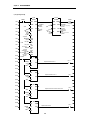
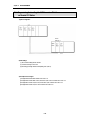
4.1 Insertion of the Function Block for A/D Conversion Module on the GMWIN
Function Block is inserted on the execution of the GMWIN according to following procedure.
Function block can be inserted only in the open condition of the Project.
Project(P)
select
Library Insert(I)
G3F – AD4A
1. Special.3fb
. AD4INI
. AD4ARD
. AD4RD
2. Remote3.3fb
. ADR4INI
. ADR4RD
3. Remote4.3fb
. ADR4INI
. ADR4RD
G4F – AD2A
1. Special.4fb
. AD2INI
. AD2ARD
. AD2RD
2. Remote4.4fb
. ADR2INI
. ADR2RD
3. Remote3.4fb
. ADR4INI
. ADR4RD
G3F – AD4B
1.Special.3fb
. AD4BINI
. AD4BARD
. AD4BRD
2.Remote3.3fb
. ADR4BINI
. ADR4BRD
3.Remote4.3fb
. ADR4BINI
. ADR4BRD
Local
Function block
Inserting
Remote GM3
Function block
Inserting
Remote GM4
Function block
Inserting
Local
Function block
Inserting
Remote GM4
Function block
Inserting
Remote GM3
Function block
Inserting
4 -1
Chapter 4. FUNCTION BLOCK
4.2 Local Function Block
4.2.1 Module Initialization : (G3F-AD4A: AD4INI, G4F-AD2A: AD2INI, G3F-AD4B: AD4BINI)
Module Initialization function block is a program for the use in setting base location number and the slot
location number of an A/D conversion module, specifying an available channel enable, a data type for
A/D conversion, filter processing data, and average processing data.
Function
block
G3F-AD4A
(G4F-AD2A)
I/O
Input
Variable
Data
type
REQ
BOOL
BASE
USINT
SLOT
USINT
CH
BOOL
[Array]
*note1
AD4INI
(AD2INI)
REQ
DONE
BASE
STAT
SLOT
ACT
CH
DATA
TYPE
FILT
_EN
FILT
_VAL
AVG_
EN
AVG_
SEL
NUM/
TIME
IN_
SEL
*note3
DATA
TYPE
FILT
_EN
FILT
_VAL
G3F-AD4B
AD4BINI
REQ
DONE
BASE
STAT
SLOT
ACT
AVG_
EN
AVG_
SEL
CH
IN_
SEL
DATA
TYPE
FILT
_EN
FILT
_VAL
AVG_
EN
AVG_
SEL
NUM/
TIME
Output
BOOL
[Array]
BOOL
[Array]
*note1
BOOL
[Array]
*note2
USINT
[Array]
*note2
BOOL
[Array]
*note2
BOOL
[Array]
*note2
NUM/
TIME
USINT
[Array]
*note2
DONE
BOOL
STAT
USINT
ACT
BOOL
[Array]
*note1
Descriptions
Function Block Execution Request Area
- The execution of function block initialization is requested in this area.
- If the status to be connected with this area is satisfied on the program operation and
input condition changes from low(0) to high(1), function bl ock initialization for the
module is executed.
Base Location Number Area
- The base No. on which A/D conversion module is mounted is written on this area.
- Setting range : GM1 series( 0 to 31 ), GM2 series( 0 to 7), GM3/4 series( 0 to 3)
Slot Location Number Area
- The slot No. on which A/D conversion module is mounted is written on this area.
- Setting range: 0 to 7
Available Channel Specification Area
- Available channels are specified in this area.
- Enabled channels are specified to 1 and disabled channels are specified to 0.
Analog Input Type(current/voltage) Specification Area
- 0 is for the select of current input
- 1 is for the select of voltage input
Output Data Type Specification Area
- Output digital data type for each channel is specified in this area.
- 0 is for the range of -192 to 16191. (G3F-AD4B: 0~16000)
- 1 is for the range of -8192 to 8191. (G3F-AD4B: -8000~8000)
Filter Processing Enable Specification Area
- 0 is for the sampling processing.
- 1 is for the filter processing.
Filter Constant Setting Area
- Setting range: 1 to 99
Average Processing Enable Specification Area
- 1 is for the average processing.
- 0 is for the sampling process.
Average process Type Specification Area
- 1 is for the time average.
- 0 is for the numb er average.
Average Number or Average Time Set Area
- The number or time is set in accordance with the average process type
specified on the AVG_SEL.
- Average number :2 to 4000 (count)
- Average time : G3F-AD4A/G3F-AD4B: 96 to12,000(ms), G4F-AD2A: 40 to 20,000(ms)
Function Block Execution Complete Area
- When function block initialization is executed with no error, 1 is written and until next
execution, 1 is continuing. When error occurs, 0 is written and operation come to stop.
Error Code Display Area
- When error occurs during function block initialization, the error code number is written.
- Error code is referred to GM Section 1.4.
Channel Operation Display Area
- The channel specified after executing the function block initialization with no error is
right, 1 is written and, on the non-specified channel, 0 is written.
REMARK
*note 1 : The number of array is G3F-AD4A of 16, G3F-AD4B of 16 and G4F-AD2A of 4 .
*note 2 : The number of array is G3F-AD4A of 4, G3F -AD4B of 16 and G4F-AD2A of 4 .
On the G3F -AD4A, the element number (0) is specified to channel 0, 1, 2, 3 in block,
the element number (1) is specified to channel 4, 5, 6, 7, in block.
the element number (2) is specified to channel 8, 9, 10, 11 in block.
the element number (3) is specified to channel 12, 13, 14, 15 in block.
On the G4F -AD2A, the element numbers means the channel ones.
*note 3 : Only on the G3F-AD4B, the number of array is 16, the element numbers means the channel ones.
4 -2
Chapter 4. FUNCTION BLOCK
4.2.2 Module Reading-Array Type : (G3F-AD4A : AD4ARD, G4F-AD2A : AD2ARD, G3F-AD4B :
AD4BARD)
Array type of function block for reading the module is performed for every channel in block and the specified
channels are used to read output variable of data displayed from A/D conversion digital value.
Function
Block
I/O
Variable
Data
type
REQ
BOOL
Function Block Execution Request Area
- The execution of function block reading is requested in this area.
- If the status to be connected with this area is satisfied on the program operation
and input condition changes from low(0) to high(1), function block initialization for
the module is executed.
BASE
USINT
Base Module Location Number Area
- The base No. on which A/D conversion module is mounted is written on this area.
- Setting range : GM1 series( 0 to 31 ), GM2 series( 0 to 7), GM3/4 series( 0 to 3)
SLOT
USINT
Slot Location Number Area
- The slot No. on which A/D conversion module is mounted is written on this area.
- Setting range: 0 to 7
CH
BOOL
[Array]
*note1
Available Channel Specification Area
- Available channels are specified in this area.
- Enabled channels are specified to 1 and disabled channels are specified to 0.
DONE
BOOL
Function Block Execution Complete Area
- When function block reading is execute d with no error, 1 is written and until next
execution, 1 is continuing. When error occurs, 0 is written and operation come to
stop
STAT
USINT
Error Code Display Area
- When error occurs during function block reading, the error code number is written.
- Error code is referred to Section 4.4.
ACT
BOOL
[Array]
*note1
Channel Operation Display Area
- The channel specified after executing the function block read with no error is
right, 1 is written and, on the non-specified channel, 0 is written
DATA
INT
[Array]
*note1
A/D Conversion Value Output Area
Input
G3F-AD4A
(G3F-AD4B,
G4F-AD2A)
AD4ARD
(AD4BARD,
AD2ARD)
REQ
DONE
BASE
STAT
SLOT
ACT
CH
Descriptions
DATA
Output
REMARK
*note 1: The number of array is G3F-AD4A of 16, G3F-AD4B of 16 and G4F-AD2A of 4 ,
the element numbers means the channel ones.
4 -3
Chapter 4. FUNCTION BLOCK
4.2.3
Module Reading - Single Type : (G3F-AD4A : AD4RD, G4F-AD2A : AD2RD, G3F-AD4B
: AD4BRD)
Single type of function block for reading the module is performed for only one channel and the specified
channel is used to read output variable of data displayed from A/D conversion digital value.
Function
Block
I/O
Variable
Data
type
BOOL
Function Block Execution Request Area
- The execution of function block reading is requested in this area.
- If the status to be connected with this area is satisfied on the program
operation and input condition changes from low(0) to high(1), function
block initialization for the module is executed.
USINT
Base Module Location Number Area
- The base No. on which A/D conversion module is mounted is written on
this area.
- Setting range : GM1 series( 0 to 31 ), GM2 series( 0 to 7), GM3/4 series( 0
to 3)
SLOT
USINT
Slot Location Number Area
- The slot No. on which A/D conversion module is mount ed is written on this
area.
- Setting range: 0 to 7
CH
USINT
Available Channel Specification Area
- Available channels are specified in this area.
- Setting range: G3F -AD4A/G3F-AD4B : 0 to 15, G4F -AD2A : 0 to 3
BOOL
Function Block Execution Complete Area
- When function block reading is executed with no error, 1 is written and until
next execution, 1 is continuing. When error occurs, 0 is written and
operation come to stop.
STAT
USINT
Error Code Display Area
- When error occurs during function block initialization, the error code
number is written.
- Error code is referred to Section 4.4.
DATA
INT
A/D Conversion Value Output Area
Input
REQ
G3F-AD4A
(G3F-AD4B,
G4F-AD2A)
AD4RD
(AD4BRD,
AD2RD)
REQ
DONE
BASE
STAT
SLOT
ACT
CH
BASE
DATA
Descriptions
Output
DONE
4 -4
Chapter 4. FUNCTION BLOCK
4.3 Remote Function Block
4.3.1 Module Initialization : (G3F-AD4A: ADR4INI, G4F-AD2A: ADR2INI, G3F-AD4B: ADR4BINI)
Function
Block
G3F-AD4A
(G4F-AD2A)
Module Initialization function block is a program for the use in setting the location number of the slot on
which the communication module of A/D conversion module of the master station is mounted, the address
number of communication module which a remote I/O station has, the base location number, and the slot
location number, and specifying the available channel enable, a data type for A/D conversion, filter process
data, and average process data.
I/O
Input
ADR4INI
(ADR2INI)
REQ
NDR
NET_
NO
ST_N
O
BASE
ERR
STAT
Variable
REQ
BOOL
NET_
NO
USINT
ST_NO
USINT
BASE
USINT
SLOT
USINT
ACT
SLOT
CH
DATA
TYPE
FILT
_EN
FILT
_VAL
AVG_
EN
AVG_
SEL
NUM/
TIME
CH
IN_
SEL*note3
G3F-AD4B
REQ
NDR
NET_
NO
ST_N
O
ERR
BOOL
[Array]
*note1
FILT
_EN
BOOL
[Array]
*note2
USINT
[Array]
*note2
BOOL
[Array]
*note2
BOOL
[Array]
*note2
AVG_
EN
STAT
AVG_
SEL
ACT
BOOL
[Array]
*note1
BOOL
[Array]
DATA
TYPE
FILT
_VAL
ADR4BINI
BASE
Data
type
SLOT
CH
IN_
SEL
DATA
TYPE
FILT
_EN
FILT
_VAL
AVG_
EN
AVG_
SEL
NUM/
TIME
Output
NUM/
TIME
USINT
[Array]
*note2
NDR
BOOL
ERR
BOOL
STAT
USINT
ACT
BOOL
[Array]
*note1
Descriptions
Function Block Execution Request Area onRising Edge.
- The execution of write function block is requested in this area.
- If the status to be connected with this area is satisfied on the program operation and input
condition changes from low(0) to high(1), function block initialization for the module is executed.
The location number of the slot on which the transmission module of the master station is
mounted. -Setting range: 0 to 7
Station number of thecommunication module which a remote I/O station has.
- Setting range : 0 to 63
Base Location Number Area
- The base No. on which A/D conversion module is mounted is written on this area.
- Setting range : 0 to 3
Slot Location Number Area
- The slot No. on which A/D conversion module is mounted is written on this area.
- Setting range: 0 to 7
Available Channel Specification Area
- Available channels are specified in this area.
- Enabled channels are specified to 1 and disabled channels are specified to 0.
Analog Input Type(current/voltage) Specification Area
- 0 is for the select of current input. – 1 is for the select of voltage input.
Output Data Type Specification Area
- Output digital data type for each channel is specified in this area.
- 0 is for the range of -192 to 16191. (G3F-AD4B : 0 ~ 16000)
- 1 is for the range of -8192 to 8191. (G3F-AD4B : -8000 ~ 8000)
Filter Process En able Specification Area
- 0 is for the sampling processing. - 1 is for the filter processing.
Filter Constant Setting Area
- Setting range: 1 to 99
Average Process Enable Specification Are a
- 1 is for the average processing. - 0 is for the sampling process.
Average process Type Specification Area
- 1 is for the time average. - 0 is for the number average.
Average Number or Average Time Set Area
- The number or time is set in accordance with the average process type
specified on the AVG_SEL.
- Average number :2 to 4000(count)
- Average time : G3F-AD4A/G3F-AD4B: 96 to12,000(ms), G4F-AD2A: 40 to 20,000(ms)
When function block execution is completed with no error, 1 is written. During the scan which the
execution condition has been made, 1 is continuing and at the next scan. 0 is written.
Error Data Display Area
- When error occurs during function block initialization, 1 is written and the operation comes
to stop. During the scan which the execution condition has been made, 1 is continuing
and at the next scan, 0 is written.
Error Code Display Area
- When error occurs during function block initialization, the error code number is written.
- Error code is referred to Section 4.4.
Channel Operation Display Area
- The channel specified after executing the function block initialization with no error is
right, 1 is written and, on the non-specified channel, 0 is written.
REMARK
*note 1 : The number of array is G3F-AD4A of 16, G3F-AD4B of 16 and G4F-AD2A of 4 .
*note 2 : The number of array is G3F-AD4A of 4, G3F-AD4B of 16 and G4F-AD2A of 4.
On the G3F-AD4A, the element number (0) is specified to channel 0, 1, 2, 3 in block,
the element number (1) is specified to channel 4, 5, 6, 7, in block.
the element number (2) is specified to channel 8, 9, 10, 11 in block.
the element number (3) is specified to channel 12, 13, 14, 15 in block.
On the G4F-AD2A, the element numbers means the channel ones.
*note 3 : Only on the G3F-AD4B, the number of array is 16, the element numbers means the channel ones.
4 -5
Chapter 4. FUNCTION BLOCK
4.3.2
Module Reading: (G3F-AD4A: ADR4RD, G4F-AD2A: ADR2RD, G3F-AD4B: ADR4BRD)
Function block for reading the module is performed for every channel in block and the specified channels
are used to read output variable of data displayed from A/D conversion digital value.
Function
Block
I/O
Input
G3F-AD4A
(G3F-AD4B,
G4F-AD2A)
Variable
Data
type
REQ
BOOL
Function Block Execution Request Area
- The execution of read function block is requested in this area.
- If the status to be connected with this area is satisfied on the program operation
and input condition changes from low(0) to high(1), function block reading for the
module is executed.
NET_
NO
USINT
The location number of the slot on which the communication module of the master
station is mounted.
- Setting range: 0 to 7
ST_NO
USINT
The station number of the communication module which a remote I/O station has.
- Setting range : 0 to 63
BASE
USINT
Base Module Location Number Area
- The base No. on which A/D conversion module is mounted is written on this area.
- Setting range : 0 to 3
SLOT
USINT
Slot Location Number Area
- The slot No. on which A/D conversion module is mounted is written on this area.
- Setting range: 0 to 7
CH
BOOL
[Array]
*note1
Available Channel Specification Area
- Available channels are specified in this area.
- Enabled channels are specified to 1 and disabled channels are specified to 0.
NDR
BOOL
When function block execution is completed with no error, 1 is written. During the scan
which the execution condition has been made, 1 is continuing and at the next scan. 0
is written.
ERR
BOOL
Error Data Display Area
- When error occurs during the execution of function block reading, 1 is written and
the operation come s to stop. During the scan which the execution condition has
been made, 1 is continuing and atthe next scan, 0 is written.
STAT
USINT
Error Code Display Area
- When error occurs during the execution of function block reading, the error code
number is written.
- Error code is referred to Section 4.4.
ACT
BOOL
[Array]
*note1
Channel Operation Display Area
-The channel specified after executing the function block reading with no error is
right, 1 is written and, on the non-specified channel, 0 is written.
DATA
INT
[Array]
*note1
A/D Conversion Value Output Area
ADR4RD
(ADR4BRD,
ADR2RD)
REQ
NDR
NET_
NO
ERR
ST_N
O
STAT
BASE
ACT
SLOT
DATA
CH
Output
Descriptions
REMARK
*note 1: The number of array is G3F-AD4A of 16, G3F-AD4B of 16 and G4F-AD2A of 4 ,
the element numbers means the channel ones.
4 -6
Chapter 4. FUNCTION BLOCK
4.4 Errors on Function Block
This shows errors and resolutions in accordance with them.
STAT
No.
Local
/Remote
0
Descriptions
Operating with no fault
Local
Function block
Read
Initiali-za
Array Single
tion
type
type
О
О
О
Resolutions
Correct the number in accordance with the
proper range
(See Section 4.2)
Contact the service station
1
The base location number is exceeding
the proper setting range
О
О
О
2
H/W error of the base
О
О
О
О
О
О
О
О
О
О
О
О
-
-
О
Specify the available channel correctly
The slot location number is exceeding
3
the proper setting range
The A/D conversion module on the slot is
empty
4
5
The module loaded isn't the A/D module
The channel number is exceeding the
proper range
H/W error of the A/D conversion module
6
7
Set the right number to the slot loading the A/D
conversion module
Load the A/D conversion module to the specified
slot
Load the A/D conversion module to the specified
slot
О
О
О
Contact the service station
8
The A/D conversion module's shared
memory error
О
О
О
Contact the service station
9
The available channels are not specified
-
О
О
10
Test mode
-
О
О
16
Filter value exceeding the proper range
О
-
-
17
Average number/time value exceeding
the proper range
О
-
H/W error of the communication module
for remote
О
О
129
The base location number is exceeding
the proper setting range
О
О
131
The slot location number is exceeding
the proper setting range
О
О
133
The module loaded isn't the A/D module
О
О
135
H/W error of the A/D conversion module
О
О
136
The A/D conversion module's shared
memory error
О
О
137
The available channels are not specified
-
О
138
Test mode
-
О
144
Filter value exceeding the proper range
О
-
128
Remote
-
Make a correct specification of the available
channel on the initialize function block
Transmit the test mode to normal mode
(G4F-AD2A only)
Correct the value to the range of 1 to 99
Correct the value to the proper range
(Number:2 to 4,000
Time: G3F-AD4A, G3F-AD4B 96 to 12,000(ms)
G4F-AD2A 40 to 20,000(ms))
See the manual for the remote communication
module
Correct the number in accordance with the
proper range
(See Section 4.2)
Set the right number to the slot mounting the
A/D conversion module
Mount the A/D conversion module to the
specified slot
Contact the service station
-
Contact the service station
Make a correct specification of the available
channel on the initializing function block
Transmit the test mode to normal mode
(G4F-AD2A only)
Correct the value to the range of 1 to 99
Correct the value to the proper range
145
Average number/time value exceeding
the proper range
О
4 -7
-
(Number:2 to 4,000
Time: G3F-AD4A, G3F-AD4B 96 to 12,000(ms)
G4F-AD2A 40 to 20,000(ms))
Chapter 5. GM PROGRAMMING
Chapter 5.
GM PROGRAMMING
5.1 Programming for Distinction of A/D Conversion Value
1) System Configuration
GM3PA1A
GM3CPUA
G3FAD4A
G3QRY4A
2) Initial Settings
(1) Available channel enable : channel 0, 2, 4
(2) Conversion data range: -192 to 16191(channel 0, 2, 4)
(3) Filter channel enabled : channel 0
(4) Filter constant setting : channel 0 = 50
(5) Average processing setting : channel 2, 4
(6) Number average setting and set value : channel 2 = 100 count
(7) Time average setting and set value : channel 4 = 200 ms
(8) Analog input : current input(DC –20 ~ 20 mA)
3) Descriptions of the Program
(1) The digital value less than 12,000 of channel 0 turns %Q0.1.0 on.
(2) The digital value more than 13,600 of channel 2 turns %Q0.1.1 on.
(3) The digital value more than 12,000 or same, and less than 13,600 or same of channel 4 turns %Q0.1.2 on.
(4) The digital value of the same as 12,800 of channel 4 turns %Q0.1.3 on.
4) Programming
(1) G3F-AD4A
A) Precautions of the programming
REMARK
- In the Initial setting
1) At the part of (3), if channel 0 is enabled to the filter processing, channel 0 to 3 will be enabled to the filter processing in block.
2) At the part of (4), if channel 0 is enabled to the filter constant, channel 0 to 3 will be enabled to the filter constant of 50in block.
3) At the part of (5), if channel2 and 4 are enabled to the average processing, channel 0 to 3 and 4 to 7 will be enabled to the average processing in block.
4) At the part of (6),if channel 2 is enabled to the number average value of 100, channel 0 to3 will be enabled to the number average value of
100 in block.
5) At the part of (7), if channel 4 is enabled to the time average value of 200ms, channel 4 to 7 will be enabled to the time average value of
200 ms in block.
5 -1
Chapter 5. GM PROGRAMMING
B) Programming Example
Normal completion of
A/D conve rsion reading
execution condition
Base location
specification
number
location number
Error code display in the Base
function block initialization specification
Error code display in the processing
of the read function block
Slot
location
specification
number
Slot location number
Channel operation display specification
in the function block
initialization
Available channel
enable specification
Channel operation display in the
processing of read function block
initialization
Data display of A/D conversion
value of enabled channel
Available channel
enable specification
Data type specification
Filter enable/disable
specification
Filter value specif ication
Average processing
enable/disable specification
Average number/time
specification
Average number/time
value specification
The digital value less than 12000 of channel 0 turns %Q0.1.0 on.
A/D conversion
value of channel 0
The digital value more than 13600 of channel 2 turns %Q0.1.1 on.
A/D conversion
value of channel 2
The digital value more than 12000 or same, and less than 13600 or
same of channel 4 turns %Q0.1.2 on.
A/D conversion
value of channel 4
The digital value 12800 of channel 4 turns %Q0.1.3 on.
A/D conversion
value of channel 4
5 -2
Chapter 5. GM PROGRAMMING
C) Specifying initial value of input/output variables on the program.
(a) Specifying channels
Select this
and this screen appears
This denotes
16 channels
Select this
and this screen appears
To select
previous Ch.
Channel No.
To select
next Ch.
Enabled channel : 1
Disabled channel : 0
To specify channel enable/disable
5 -3
Chapter 5. GM PROGRAMMING
(b) Specifying filter enable/disable
To specify G3F -AD4A channel 0,1,2, 3 in block
To specify G3F -AD4A channel 4,5,6,7 in block
To specify G3F -AD4A channel 8,9,10,11 in block
To specify G3F -AD4A channel 12,13,14,15 in block
Filter enable : 1
Filter disable : 0
To specify filter enable/disable
5 -4
Chapter 5. GM PROGRAMMING
D) Input/output variables on Programming
Variable Name
Var_Kind
AD_CH
AD_INI
AD_RD
AVG_EN
AVG_SEL
DATA
DATATYPE
FILT_EN
FILT_VAL
INI_ACT
INI_STAT
NUM_TIME
RD_ACT
RD_STAT
READY
START
Data Type
: VAR
: VAR
: VAR
: VAR
: VAR
: VAR
: VAR
: VAR
: VAR
: VAR
: VAR
: VAR
: VAR
: VAR
: VAR
: VAR
: ARRAY [0..15] OF BOOL
: FB instance
: FB instance
: ARRAY [0..3] OF BOOL
: ARRAY [0..3] OF BOOL
: ARRAY [0..15] OF INT
: ARRAY [0..15] OF BOOL
: ARRAY [0..3] OF BOOL
: ARRAY [0..3] OF USINT
: ARRAY [0..15] OF BOOL
: USINT
: ARRAY [0..3] OF UNIT
: ARRAY [0..15] OF BOOL
: USINT
: BOOL
: BOOL
(AT Address) (Initial Value)
: = { 1,0,1,0,1,0,0,0,0,0,0,0,0,0,0,0 }
: = { 1,1,0,0 }
: = { 0,1,0,0 }
: = { 0,0,0,0,0,0,0,0,0,0,0,0,0,0,0,0 }
: = { 1,0,0,0 }
: = { 50,0,0,0 }
: = { 100,200,0,0 }
(2) G3F-AD4B
A) Input/output variables on Programming
Variable Name
AD_CH
AD_INI
AD_RD
AVG_EN
AVG_SEL
DATA
DATATYPE
FILT_EN
FILT_VAL
INI_ACT
IN_SEL
INI_STAT
NUM_TIME
RD_ACT
RD_STAT
READY
START
Var_Kind
※1
※2
※3
※4
※5
※6
Data Type
: VAR
: VAR
: VAR
: VAR
: VAR
: VAR
: VAR
: VAR
: VAR
: VAR
: VAR
: VAR
: VAR
: VAR
: VAR
: VAR
: VAR
: ARRAY [0..15] OF BOOL
: FB instance
: FB instance
: ARRAY [0..15] OF BOOL
: ARRAY [0..15] OF BOOL
: ARRAY [0..15] OF INT
: ARRAY [0..15] OF BOOL
: ARRAY [0..15] OF BOOL
: ARRAY [0..15] OF USINT
: ARRAY [0..15] OF BOOL
: ARRAY [0..15] OF BOOL
: USINT
: ARRAY [0..15] OF UNIT
: ARRAY [0..15] OF BOOL
: USINT
: BOOL
: BOOL
(AT Address) (Initial Value)
: = { 1,0,1,0,1,0,0,0,0,0,0,0,0,0,0,0 }
: = { 0,0,1,0,1,0,0,0,0,0,0,0,0,0,0,0 }
: = { 1,0,1,0,1,0,0,0,0,0,0,0,0,0,0,0 }
: = { 0,0,0,0,0,0,0,0,0,0,0,0,0,0,0,0 }
: = { 1,0,0,0,0,0,0,0,0,0,0,0,0,0,0,0 }
: = { 50,0,0,0,0,0,0,0,0,0,0,0,0,0,0,0 }
: = { 0,0,0,0,0,0,0,0,0,0,0,0,0,0,0,0 }
: = { 0,0,100,0,200,0,0,0,0,0,0,0,0,0,0,0 }
B) The difference of G3F-AD4A and G3F-AD4B
(a) It is different only to input variable of initial function block
(b) ※1 is used only to the G3F-AD4B
(c) ※2,※3,※4,※5,※6 are filter and average processing function, it is processed 4 channel in block of
the G3F-AD4A and is processed every channel of the G3F-AD4B
Section
※1
※2
※3
※4
※5
※6
Input
Variable
Name
AVG_EN
AVG_SEL
FILT_EN
FILT_VAL
IN_SEL
NUM_TIME
Variable
Name
AVG_EN
AVG_SEL
FILT_EN
FILT_VAL
NUM_TIME
G3F-AD4A
Data type
ARRAY[0..3] OF BOOL
ARRAY[0..3] OF BOOL
ARRAY[0..3] OF BOOL
ARRAY[0..3] OF USINT
ARRAY[0..3] OF USINT
5 -5
Variable
Name
AVG_EN
AVG_SEL
FILT_EN
FILT_VAL
IN_SEL
NUM_TIME
G3F-AD4B
Data type
ARRAY[0..15] OF BOOL
ARRAY[0..15] OF BOOL
ARRAY[0..15] OF BOOL
ARRAY[0..15] OF USINT
ARRAY[0..15] OF BOOL
ARRAY[0..15] OF USINT
Remark
Only G3F-AD4B
Chapter 5. GM PROGRAMMING
C) Programming Example
AD_INI
AD4BINI
READY
Line 0
Execution condition
Line 1
0
Base location number
specification
Line 2
0
Slot location number
specification
Line 3
Line 4
Line 5
REQ
AD_CH
Available channel
Enable specfication
IN_SEL
Input type specfication
AD_RD
AD4BARD
DONE
BASE
STAT
ACT
SLOT
CH
REQ
INI_STAT
Error code display in the
function block initialization
specfication
INI_ACT
러정보
Channel operation display
In the function block
initialization
0
BASE
STAT
0
SLOT
ACT RD_ACT
Base location number
specfication
Slot location number
AD_CH
Available channel
Enable specfication
IN_
SEL
START
S
DONE
CH
RD_STAT
Normal completion of
A/D conversion reading
Error code display in the processing
of the read function block
Channel operation display in the
processingof read function block
DATA DATA
Data display of A/D conversion
value of enabled channel
DATA
TYPE
FILT_EN FILT
Filter enable/disable specfication
_EN
FILT
FILT_VAL
_VAL
Filter value specfication
AVG_
AVG_EN
EN
Average processing
enable/disable specfication
AVG_
AVG_SEL SEL
Average number/time specfication
NUM/
NUM_TIME
TIME
Average number/time
DATATYPE
Data type specfication
Line 6
Line 7
Line 8
Line 9
Line 10
value specfication
START
Line 11
Line 12
DATA[0]
Line 13
2000
A/D conversion value
of channel 0
LT
EN
OUT
IN1
OUT
The digital value less than 2000 of channel 0 turns %Q0.1.0 On
%Q0.1.0
IN2
Line 14
GT
Line 15
Line 16
Line 17
EN
DATA[2]
A/D conversion value
of channel 2
3600
ENO
IN1
OUT
The digital value more than 3600 of channel 2 turns %Q0.1.1 On
%Q0.1.1
IN2
Line 18
GE
Line 19
EN
ENO
OUT
Line 20
3600
IN1
Line 21
DATA[4]
IN2
Line 22
A/D conversion vaule
of channel 4
2000
The digital value more than 2000 or same, and less than 3600 or same of channel 4 turns %Q0.1.2 On
%Q0.1.2
IN3
Line 23
EQ
Line 24
Line 25
DATA[4]
A/D conversion value
of channel 4
2800
EN
ENO
IN1
OUT
The digital value 2800 of channel 4 turns %Q0.1.3 On
IN2
5 -6
%Q0.1.3
Chapter 5. GM PROGRAMMING
7.2 Programming for Display of A/D Conversion Value and Error Code on BCD
Display
1) System Configuration
Initial
setting
Digital
conversion
Digital
2) Initial Settings
(1) Available channel enabled : channel 0,
(2) Time average processing specification: 100 ms
(3) Data output type setting: -192 to 16191
(4) Analog input : current input(DC -20 to 20 mA)
3) Descriptions of the Program
(1) % I0.1.0 turning On leads to the initial setting of A/D conversion module.
(2) % I0.1.1 turning On leads to displaying A/D conversion value on the BCD display.(%Q0.1.0 to %Q0.1.19)
(3) % I0.1.2 turning On leads to displaying error code of function block on the BCD display,
(%Q0.2.0 to %Q0.2.7)
5 -7
conversion
Chapter 5. GM PROGRAMMING
4) Programming
A/D conversion read has
been completed normally.
Execution condition and
Initial Setting
Base location
specification
number
Error
code display
display ininthe
the Base location number
Error code
processing
function specification
function blockofinitialization
block initialization
Error code display in the processing
of the reading function block
Slot
Slot location
location
specification
specification
number
number
Channel operation display
in the function block
initialization
Slot location number
specification
Data display of A/D conversion
value of enabled channel
Available channel
enable specification
Available channel
enable specification
Data type specification
Filter enable/disable
specification
Filter value specification
Average processing
enable/disable specification
Average number/time
specification
Average number/time
value specification
This program converts the integer type of the A/D conversion value
CH0_DATA into BCD data type to display onto the BDC digital display.
Command for displaying the
A/D conversion value onto BCD
digital display
A/D conversion
value of channel
0
Command for displaying the
error code onto BCD digital
display
Error code on the
reading function
This program converts the unsigned integer type of RD_STAT, which indicates the err or status
of the reading function block, into BCD data type to display it onto the BDC digital display.
5 -8
Chapter 5. GM PROGRAMMING
5) Input/output variables on the programming
Variable Name
Var_Kind
Data
AD_CH
: VAR
AD_INI
: VAR
: FB Instance
AD_RD
: VAR
: FB Instance
AVG_EN
: VAR
AVG_SEL
: VAR
CH0_DATA
: VAR
DATA
DATATYPE
FILT_EN
FILT_VAL
: VAR
: VAR
: VAR
: VAR
INI_ACT
: VAR
INI_STAT
: VAR
NUM_TIME
: VAR
Type
(AT Address) (Initial Value)
: ARRAY [0..15] OF BOOL : = {1,0,0,0,0,0,0,0,0,0,0,0,0,0,0,0}
: ARRAY [0..3] OF BOOL
: ARRAY [0..3] OF BOOL
: = {1,0,0,0}
: = {1,0,0,0}
: INT
: DINT
:ARRAY [0..15] OF BOOL
: = {0,0,0,0,0,0,0,0,0,0,0,0,0,0,0,0}
: ARRAY [0..3] OF BOOL
: = {0,0,0,0}
: ARRAY [0..3] OF USINT
: = {0,0,0,0}
: ARRAY [0..15] OF BOOL
: USINT
: ARRAY [0..3] OF UINT : = {100,0,0,0}
RD_STAT
: VAR
: USINT
START
: VAR
: BOOL
5 -9
Chapter 5. GM PROGRAMMING
7.3 Programming for Loading the A/D Conversion Module
on Remote I /O Station
1) System Configuration
Remote
Station No. “1”
2) Initial Settings
(1) A/D conversion enabling channel: channel 0
(2) Conversion data range: -192 to 16191
(3)Time average processing channel: channel 0(setting value: 1,000 ms)
3) Descriptions of the Program
(1)The digital value less than 8000of channel 0 turns %Q0.1.0 on.
(2)The digital value more than 8000 or same, and less than 10,000 or same of channel 0 turns %Q0.1.1 on.
(3)The digital value more than 10,000 or same, and less than 12,000 of channel 0 turns %Q0.1.2 on.
(4)The digital value more than 12,000 or same of channel 0 turns %Q0.1.3 on.
5 -10
Chapter 5. GM PROGRAMMING
4) Programming example
Execution condition
and initial setting
Execution request when
the initializing function
block is not operated
It indicates on when operated
normally, and off when operated
abnormally or down from Live data
of opposite station
Slot location number of master
communication module
Address of remote station
Base location number of A/D
conversion module
It indicates information on
power-off state of opposite
station. If restored, it turns
“On” and the “On” state is
retained until the user
program turns it “Off”.
Error data display in processing
of initialization function block
Error code display in processing
of initialization function block
Normal channel operation
display
Slot location number of A/D
conversion module
Available channel enable
specification
Conversion data range
specification
Execution request on the reading
function block with communication
intervals.
Slot location number of master
communication module
Filter enable/disable
specification
Error data display
Filter constant specification
Address of remote station
Error code display at
occurring error
Average processing
enable/disable specification
Base location number of A/D
conversion module
Normal channel operation
display
Average processing
number/time specific ation
Slot location number of A/D
conversion module
A/D conversion value
Number/time constant
specification
Available channel enable
specification
The digital value less
than 8000 of channel 0
turns %Q0.1.0 on.
The digital value more
than 8000 or same, and
less than 10000 or same
turns %Q0.1.1 on.
The digital value more
than 10000 or same,
and less than 12000
turns %Q0.1.2 on.
The digital value more
than 12000 or same
turns %Q0.1.3 on.
5 -11
Chapter 5. GM PROGRAMMING
5) Input/output variables used on the programming
Variable Name
AD_CH
AD_DATA
Var_Kind
: VAR
: VAR
Data
Type
: ARRAY [0..3] OF BOOL
(AT Address) (Initial Value)
: = {0,0,0,0}
: ARRAY [0..3] OF INT
AD_INI
: VAR
: FB Instance
AD_RD
: VAR
: FB Instance
AVG_EN
: VAR
: ARRAY [0..3] OF BOOL
: = {1,0,0,0}
AVG_SEL
: VAR
: ARRAY [0..3] OF BOOL
: = {1,0,0,0}
DATATYPE
FILT_EN
FILT_VAL
: VAR
: VAR
: VAR
:ARRAY [0..3] OF BOOL
: ARRAY [0..3] OF BOOL
: = {0,0,0,0}
: ARRAY [0..3] OF USINT
: = {0,0,0,0}
INI_ACT
: VAR
: ARRAY [0..3] OF BOOL
INI_ERR
: VAR
: BOOL
INI_STAT
NUM_TIME
RD_STAT
: VAR
: VAR
: VAR
: = {0,0,0,0}
: USINT
: ARRAY [0..3] OF UINT
: ARRAY [0..3] OF BOOL
RD_ERR
: VAR
: BOOL
RD_STAT
: VAR
: USINT
READY
: VAR
: BOOL
5 -12
: = {1000,0,0,0}
Chapter 6. BUFFER MEMORY CONFIGURATION AND FUNCTION
Chapter 6. BUFFER MEMORY CONFIGURATION AND FUNCTION
The A/D conversion module has a buffer memory for communication of data with the PLC CPU.
6.1 Buffer Memory Configuration
6.1.1 G3F-AD4A buffer memory
Address
(Decimal)
Descriptions
Detail descriptions
Non-initialization
0.
Available channel specification
Bit on(1):Channel enable, Bit off(0):Channel disable
1.
Data output type specification
Bit on(1): -8192 to 8191, Bit off(0): -192 to 16191
2.
Filter processing specification
Bit on(1):Filter processing , Bit off(0):Sampling processing
Process by sampling
3.
Filter constant setting to channel 0,1,2,3
4.
Filter constant setting to channel 4,5,6,7
5.
Filter constant setting to channel 8,910,11
Setting range:1 to 99
Set the filter constant to "1"
6.
Filter constant setting to channel 12,13,14,15
7.
Average processing specification
Bit on(1):Average processing , Bit off(0 ):Sampling processing
Process by sampling
8.
Time/number average specification
Bit on(1):Time average, Bit off(0):Number average
Specify to number average
Setting range
Time average: 96 to 12, 000(ms)
Set to the constant"96"
9.
Average time/number setting to channel 0, 1, 2, 3
10.
Average time/number setting to channel 4, 5, 6, 7
11.
Average time/number setting to channel 8, 9, 10, 11
12.
Average time/number setting to channel 12, 13, 14, 15
13.
Set data specification
14.
A/D Conversion value to channel 0
15.
A/D Conversion value to channel 1
16.
A/D Conversion value to channel 2
17.
A/D Conversion value to channel 3
18.
A/D Conversion value to channel 4
19.
A/D Conversion value to channel 5
20.
A/D Conversion value to channel6
21.
A/D Conversion value to channel 7
22.
A/D Conversion value to channel 8
23.
A/D Conversion value to channel 9
24
A/D Conversion value to channel 10
25.
A/D Conversion value to channel 11
26.
A/D Conversion value to channel 12
27.
A/D Conversion value to channel 13
28.
A/D Conversion value to channel 14
29.
A/D Conversion value to channel 15
30.
Channel operation data
31.
Error code to channel 0, 1, 2, 3
32.
Error code to channel 4, 5, 6, 7
33.
Error code to channel 8, 9, 10, 11
34.
Error code to ch annel 12, 13, 14, 15
Remark
No allowance for use
Set the data output type to
-192 to 16191
Read/write
Number average: 2 to 4,000(count)
Bit on(1):Change the buffer address 0 to 12 into
new specification value
Bit off(0):Remain the bufferof address 0 to 12 in the
previous
Non-specification
value
-
-
Read only enable
Bit on(1):Operation, Bit off(0):Operation stop
Operation stop
0 : Normal operation
16 : Filter constant setting range exceeding
17 : Average number/time constant setting range exceeding
6 -1
-
Chapter 6. BUFFER MEMORY CONFIGURATION AND FUNCTION
6.1.2 G3F-AD4B buffer memory
Address
(Decimal)
Descriptions
Detail descriptions
Non-initialization
0.
Available channel specification
Bit on(1):Channel enable, Bit off(0):Channel disable
1.
Input used specification
Bit on(1):voltage input, Bit off(0):current input
2.
Data output type specification
Bit on(1): -8000 to 8000, Bit off(0):0 to 16000
3.
Filter processing specification
Bit on(1):Filter processing , Bit off(0):Sampling processing
Process by sampling
4.
Filter constant setting to channel 0
5.
Filter constant setting to channel 1
6.
Filter constant setting to channel 2
7.
Filter constant setting to channel 3
8.
Filter constant setting to channel 4
9.
Filter constant setting to channel 5
10.
Filter constant setting to channel 6
11.
Filter constant setting to channel 7
12.
Filter constant setting to channel 8
Setting range:1 to 99
Set the filter constant to "1"
13.
Filter constant setting to channel 9
14.
Filter constant setting to channel 10
15.
Filter constant setting to channel 11
16.
Filter constant setting to channel 12
17.
Filter constant setting to channel 13
18.
Filter constant setting to channel 14
19.
Filter constant setting to channel 15
20.
Average processing specification
Bit on(1):Average processing, Bit off(0):Sampling processing
Process by sampling
21.
Time/number average specification
Bit on(1):Time average, Bit off(0):Number average
Specify to number average
22.
Average time/number setting to channel 0
23.
Average time/number setting to channel 1
24.
Average time/number setting to channel 2
25.
Average time/number setting to channel 3
26.
Average time/number setting to channel 4
27.
Average time/number setting to channel 5
28.
Average time/number setting to channel 6
29.
Average time/number setting to channel 7
30.
Average time/number setting to channel 8
Setting range
Time average: 96 to 12,000(ms)
Set to the constant"96"
31.
Average time/number setting to channel 9
32.
Average time/number setting to channel 10
33.
Average time/number setting to channel 11
34.
Average time/number setting to channel 12
35.
Average time/number setting to channel 13
36.
Average time/number setting to channel 14
37.
Average time/number setting to channel 15
38.
Set data specification
39.
A/D Conversion value to channel 0
40.
A/D Conversion value to channel 1
41.
A/D Conversion value to channel 2
42.
A/D Conversion value to channel 3
43.
A/D Conversion value to channel 4
44.
A/D Conversion value to channel 5
45.
A/D Conversion value to channel 6
46.
A/D Conversion value to channel 7
Remark
No allowance for use
Set to the current input
Set the data output type to 0
to 16000
Read/write
Number average: 2 to 4,000(count)
“0” Bit on(1):Change the buffer address 0 to 37 into
new specification value
“0” Bit off(0):Remain the buffer of address 0 to 37 in the
previous value
-
6 -2
Non-specification
-
Read only enable
Chapter 6. BUFFER MEMORY CONFIGURATION AND FUNCTION
Address
(Decimal)
Descriptions
47.
A/D Conversion value to channel 8
48.
A/D Conversion value to channel 9
49.
A/D Conversion value to channel 10
50.
A/D Conversion value to channel 11
51.
A/D Conversion value to channel 12
52.
A/D Conversion value to channel 13
53.
A/D Conversion value to channel 14
54.
A/D Conversion value to channel 15
55.
Channel operation data
56.
Error code to channel 0
57.
Error code to channel 1
58.
Error code to channel 2
59.
Error code to channel 3
60.
Error code to channel 4
61.
Error code to channel 5
62.
Error code to channel 6
63.
Error code to channel 7
64.
Error code to channel 8
65.
Error code to channel 9
66.
Error code to channel 10
67.
Error code to channel 11
68.
Error code to channel 12
69.
Error code to channel 13
70.
Error code to channel 14
71.
Error code to channel 15
Detail descriptions
Non-initialization
-
-
Bit on(1):Operation, Bit off(0):Operation stop
Remark
Operation stop
Read only enable
0 : Normal operation
16 : Filter constant setting range exceeding
17 : Average number/time constant setting range exceeding
6 -3
-
Chapter 6. BUFFER MEMORY CONFIGURATION AND FUNCTION
6.1.3 G4F-AD2A buffer memory
Address
(Decimal)
0.
Descriptions
Available channel specification
Detail descriptions
Non-initialization
Bit on(1): Channel enable
Bit off(0): Channel disable
No allowance for use
Bit on(1): -8192 to 8191
Set the data output type to -192
Bit off(0): -192 to 16191
to 16191
Bit on(1): Filter processing
Bit off(0): Sampling processing
process by sampling
Setting range : 1 to 99
Set the filter constant to "1"
Bit on(1) : Average processing
Bit off( 0) : Sampling processing
Process by sampling
1.
Data output type specific ation
2.
Filter processing specification
3.
Filter constant setting to channel 0
4.
Filter constant setting to channel 1
5
Filter constant setting to channel 2
6.
Filter constant setting to channel 3
7.
Average processing specification
8.
Time/Number average specification
9.
Average time/number setting to channel 0
10
Average time/number setting to channel 1
Setting range
Time average : 40 to 20,000(ms)
11.
Average time/number setting to channel 2
umber average: 2 to 4,000 (count)
12.
Average time/number setting to channel 3
Bit on(1) : Time average
Bit off(0) : Number average
Remark
Read/Write enable
Specify to number average
Set to the constant "40"
Bit on(1):Change the bufferof address
13.
Set data specification
0 to 12
Bit off(0):Remain the buffer of address
Non-specification
0 to 12 in the precious value
14.
A/D Conversion value to channel 0
15.
A/D Conversion value to ch annel 1
16.
A/D Conversion value to channel 2
17
A/D Conversion value to channel 3
18.
Channel operation data
19.
Error code to channel 0
20
Error code to channel 1
21.
Error code to channel 2
22.
Error code to channel 3
-
Bit on(1) : Operation
Bit off(0) : Operation stop
-
Read only enable
Operation stop
0 : Normaloperation
16 : Filt er constant setting range
exceeding
17 : Average number/time constant
setting range exceeding
6 -4
-
Chapter 6. BUFFER MEMORY CONFIGURATION AND FUNCTION
6.2 Buffer Memory Functions
▶ Each address of buffer memory has been occupied by one word, and it is displayed as 16 Bit
▶ Each address is composed of 16 Bit, and each Bit can be executed by specifying Bit on to 1 or Bit off to 0
6.2.1
Available Channel Specification Area (G3F-AD4A,G3F-AD4B: address 0, G4F-AD2A: address 0)
1) A/D conversion enable/ disable can be specified for every channel.
2) Banning disabled channel conversion turns the sampling period short.
3) If enable channel isn't specified, every channel comes to be disabled.
4) A/D conversion enable/disable is like this as follows.
(1) G3F-AD4A, G3F-AD4B
Address “0”
Channel enable/disable specification [Bit Off(0): Conversion disable, Bit On(1): Conversion enable]
(2) G4F-AD2A
Address “0”
Ignored
Channel enable/disable specification
[Bit Off(0): Conversion disable, Bit On(1): Conversion enable]
6.2.2 Input Used Type Specification Area (G3F-AD4B: address 1)
1) Input used type can be specified for every channel only the G3F-AD4B
2) Input used type(current/voltage) specification is like this as follow s.
Address “1”
Input used type specification [Bit Off(0): current input, Bit On(1): voltage input]
6 -5
Chapter 6. BUFFER MEMORY CONFIGURATION AND FUNCTION
6.2.3 Data Output Type Specification Area (G3F-AD4A: address 1, G4F-AD2A: address 1, G3F-AD4B:address2)
1) Digital data output type from analog input can be specified for every channel.
2) If output data type isn't specified, every channel will be set to the range of -192 to 19161 for the G3F-AD4A
and the G4F- AD2A, and set to the range of 0 to 16000 for the G3F-AD4B.
3) Data output type specification is like this as follows.
(1) G3F – AD4A, G3F-AD4B
Address “1”
Address “2”
Output data type specification
G3F-AD4A : [Bit Off(0): -192~16191, Bit On(1): -8192~8191]
G3F-AD4B : [Bit Off(0): 0~16000, Bit On(1): -8000~8000]
(2) G4F – AD2A
Address “1”
Ignored
Output data type specification
[Bit Off(0) : -192~16191, Bit On(1) : -8192~8191]
6.2.4 Filter Processing Enable/Disable Specification Area (G3F-AD4A: address2,G4F-AD2A: address 2,
G3F-AD4B:address3)
1) Filter processing enable/disable can be specified to 4 channels of the K7F-AD4A, 1 channel of the K4F -AD2A and
the G3F -AD4B.
2) When filter processing isn't specified, sampling processes every channel.
3) Filter processing specification is as follows.
(1) G3F-AD4A
Address “2”
Ignored
6 -6
Filter processing specification
[Bit Off(0) : Sampling processing, Bit On(1) :Filter processing]
Chapter 6. BUFFER MEMORY CONFIGURATION AND FUNCTION
A) 4 bits are available, and 1 bit for filter processing is performed for continuous 4 channels in block.
Bit 0 : Filter processing enable/disable to channel 0,1,2,3 is specified in block.
Bit 1 : Filter processing enable/disable to channel 4,5,6,7 is specified in block.
Bit 2 : Filter processing enable/disable to channel 8,9,10,11 is specified in block.
Bit 3 : Filter processing enable/disable to channel 12,13,14,15 is specified in block.
B) Filter processing enable/disable to 4 channel in a bit shouldn’t be specified by channel.
(Ex. Filter processing to channel 0 and sampling processing to channel 1 shouldn't be specified.)
(2) G3F-AD4B
Address “3”
Filter processing specification
[Bit Off(0) : Sampling processing, Bit On(1) :Filter processing]
(3) G4F-AD2A
Address “2”
Ignored
Filter processing specification
[Bit Off(0) : Sampling processing, Bit On(1) :Filter processing]
6.2.5 Filter Constant Setting Area (G3F-AD4A, G4F-AD2A: address 3 to 6, G3F-AD4B: address 4 to 19)
1) Filter constant setting can be specified to 4 channels of the G3F-AD4A, 1 channel of the G4F-AD2A and the
G3F-AD4B.
2) Filter constant setting range is 1 to 99.
3) When setting value is out of the range, error code number 16 is written to buffer memory address
31 to 34(of the G3F-AD4A) and the previous data remain as A/D conversion value.
4) When filter constant isn't set, filter constant will be set to 1.
5) Filter constant setting is as follows.
Address
Filter constant setting to each channel
G3F-AD4A
G4F-AD2A
address 3 Filter constant setting in block to channel 0, 1, 2, 3
Filter constant setting to channel 0.
address 4 Filter constant setting in block to channel 4, 5, 6, 7
Filter constant setting to channel 1
address 5 Filter constant setting in block to channel 8, 9, 10, 11
Filter constant setting to channel 2
address 6 Filter constant setting in block to channel 12, 13, 14, 15
Filter constant setting to channel 3.
Remark
Before average number/time constant value is set, average processing enable/disable specifying
and number/time average processing setting have to be set.
6 -7
Chapter 6. BUFFER MEMORY CONFIGURATION AND FUNCTION
6.2.6 Average Processing Enable/ Disable Specification Area (G3F-AD4A: address7, G4F-AD2A : address 7, G3F
-AD4B : address 20 )
1) Average processing enable/disable can be specified to 4 channels of the G3F-AD4A, 1 channel of the G4F-AD2A
and 1 channel of the G3F-AD4B
2) When average processing isn't specified, every channel get processed by sampling.
3) Average processing specification is as follows.
(1) G3F-AD4A
Address “7”
Ignored
Average processing specification
[Bit Off(0) : Sampling processing,
Bit On(1) :Average processing]
A) 4 bits are available, and 1 bit for average processing is performed for continuous 4 channels in block.
Bit 0 : Average processing enable/disable to channel 0,1,2,3 is specified in block.
Bit 1 : Average processing enable/disable to channel 4,5,6,7 is specified in block.
Bit 2 : Average processing enable/disable to channel 8,9,10,11 is specified in block.
Bit 3 : Average processing enable/disable to channel 12,13,14,15 is specified in block.
B) Average processing enable/disable to 4 channel in a bit should not be specified in block.
(Ex. Average processing to channel 0 and sampling processing to channel should not be specified.)
(2) G3F-AD3B
Address “20”
Filter processing specification
[Bit Off (0): Sampling processing, Bit On (1): Average processing]
(3) G4F-AD2A
Address “7”
Ignored
6 -8
Filter processing specification
[Bit Off (0): Sampling processing,
Bit On (1): Average processing]
Chapter 6. BUFFER MEMORY CONFIGURATION AND FUNCTION
6.2.7 Number / Time Average Processing Setting Area (G3F-AD4A,G4F-AD2A: address 8, G3F-AD4B: address 21)
1) It depends on A/D conversion module channel whether average processing is followed to time or number.
(G3F-AD4A for 4 channel in block, G4F-AD2A/G3F-AD4B for ev ery channel)
2) No specification of number/time average processing leads to number average processing.
3) Number/time average processing is as follows.
(1) G3F – AD4A
Address “8”
Ignored
Number/time average processing specification
[Bit Off(0) : Number average processing,
Bit On(1) :Time average processing]
A) 4 bits are available, and 1 bit for number/time average processing setting is performed for continuous 4
channels in block.
Bit 0 : Number/time average processing to channel 0,1,2,3 is specified in block.
Bit 1 : Number/time average processing to channel 4,5,6,7 is specified in block.
Bit 2 : Number/time average processing to channel 8,9,10,11 is specified in block.
Bit 3 : Number/time average processing to channel 12,13,14,15 is specified in block.
B) Number/time average processing to 4 channel in a bit should not be specified in block.
(Ex. Number average processing to channel 0 and time average processing to channel should not be
specified.)
(2) G3F-AD4B
Address “21”
Number/time average processing specification
[Bit Off(0) : Number average processing, Bit On(1) :Time average processing]
(3) G4F – AD2A
Address “8”
Ignored
Number/time average processing specification
[Bit Off(0) : Number average processing,
Bit On(1) :Time average processing]
Remark
Before number /time average processing is set, average processing enable/disable has to be
specified.
6 -9
Chapter 6. BUFFER MEMORY CONFIGURATION AND FUNCTION
6.2.8 Average Number / Time Constant Setting Area (G3F-AD4A, G4F-AD2A : address 9 to 12, G3F-AD4B :
address 22 to 37)
1) Average number/time constant setting range is as follows.
(1) Average number setting range: 2 to 4000 (count).
(2) Average time setting range: G3F-AD4A, G3F-AD4B (96 to 12000 ms), G4F-AD2A (40 to 20000ms)
2) When setting value is out of the range, error code number 17 is written to buffer memory address 31 to
34 and the previous data remain as A/D conversion value.
3) When average number/time constant isn't set G3F-AD4A/G3F-AD4B of 96 and G4F-AD2A of 40 will
be set.
4) Average number/time constant setting is as follows.
Address
address 9
address 10
address 11
address 12
Average number/time constant setting to each channel
G3F – AD4A
G4F – AD2A
Average number/time constant setting in block to
Average number/time constant setting
channel 0, 1, 2, 3,
channel 0.
Average number/time constant setting in block to
Average number/time constant setting
channel 4, 5, 6, 7
channel 1
Average number/time constant setting in block to
Average number/time constant setting
channel 8, 9, 10, 11
channel 2
Average number/time constant setting in block to
Average number/time constant setting
channel 12, 13, 14, 15
channel 3.
REMARK
Before average number/time constant value is set, average processing enable/disable
Specifying and number/time average processing setting have to be set.
6.2.9 SET Data Specification Area (G3F-AD4A/G4F-AD2A: address 13, G3F-AD4B: address 38)
1) When specified bit of each channel isn't turned on in the SET data specification area(addr ess 13), A/D
conversion isn't executed by A/D conversion module's data which users specified address 0 to 12 and the
previous data remains.(G3F-AD4A, G4F-AD2A)
2) SET data is specified as follows.
(1) G3F – AD4A
Address “13” (2) G4F – AD2A
SET data specification [Bit Off(0) : Disable, Bit On(1) : Enable]
(2) G4F – AD2A
Address “13”
Ignored
6 - 10
SET data specification
[Bit Off (0): Disable, Bit On(1) :Enable]
Chapter 6. BUFFER MEMORY CONFIGURATION AND FUNCTION
Address“38”
Bit 15
Bit 14
—
—
Bit13
—
Bit 12
Bit 11
Bit 10
—
—
—
Bit 9
—
Bit 8
Bit7
Bit6
Bit5
Bit4
Bit3
Bit2
Bit1
Bit 0
—
—
—
—
—
—
—
Channel
0~15
(3) G3F-AD4B
—
Ignored
SET data specification
[Bit Off (0): Disable, Bit On(1) :Enable]
6.2.10 Digital Output Area (G3F-AD4A : address 14 to 29, G4F-AD2A : address 14 to 17, G3F-AD4B : address 39
to 54)
1) Digital output value to analog input value through terminals is stored in this area.
2) When error occurs, the previous digital value remains.
6.2.11 Channel Operation Data Storage Area (G3F-AD4A : address 30, G4F-AD2A : address 18, G3F-AD4B :
address 55)
Channel operation data is stored in this area.
(1) G3F – AD4A, G3F-AD4B
Address “30”
Address “55”
(2) G4F – AD2A
Address “18”
Ignored
Channel operation data
[Bit Off(0) :Stop, Bit On(1) :Normal]
6.2.12 Error Code Display Area (G3F-AD4A : address 31 to 34, G4F-AD2A : address 19 to 22, G3F-AD4B :
address 56 to 71)
1) Error code is as follows.
Error code
Descriptions
Remarks
16
Filter constant setting range exceeding
RUN LED flickering(per 0.6sec)
17
Average number/time setting range exceeding
RUN LED flickering(per 0.6sec)
6 - 11
Chapter 6. BUFFER MEMORY CONFIGURATION AND FUNCTION
2) When two types of error have occurred simultaneously, 17 and 16 are displayed in the order.
3) Error code display channel of each address is as follows.
Address
G3F-AD4A
Specified channel
Address
G4F-AD2A
Specified channel
31
error code display to channel 0, 1, 2, 3
19
error code display to channel 0
32
error code display to channel 4, 5, 6, 7
20
error code display to channel 1
33
error code display to channel 8, 9, 10, 11
21
error code display to channel 2
34
error code display to channel 12, 13, 14, 15
22
error code display to channel 3
6 - 12
Chapter 7. SPECIAL MODULE COMMAND (BUFFER MEMORY READ/WRITE)
Chapter 7. SPECIAL MODULE COMMAND (BUFFER MEMORY READ/ WRITE)
A/D conversion module occupies 16 I/O points.
7.1 Local Command
7.1.1 Buffer Memory Read - GET, GETP
<Format>
GET command
execution condition
GET
n1
n2
D
n3
Symbol
Descriptions
Device used
n1
Slot number assigned to special module
Integer
n2
First address of the buffer memory of special
module from which data are read
Integer
D
First address of device which will store read data.
M, P, K, L, T, C, D, #D
n3
Number of words of data read
Integer
< Distinction of GET and GETP>
GET: Continuously executes read while the read signal is on (
GETP: Execute read by rising edge on the read signal
(
)
)
ex 1) A/D conversion module is mounted on the slot 3 of base, and data from the buffer memory address 14 and
15 is read to the CPU D14 and D15. ( ( ) : Buffer memory address of the G3F-AD4B )
(address)
Buffer memory of
A/D conversion module
D area of CPU module
D13
(address)
13(38)
D14
A/D conversion value Ch 0
A/D conversion value Ch 0
14(39)
D15
A/D conversion value Ch 1
A/D conversion value Ch 1
15(40)
D16
16(41)
D17
17(42)
<GET>
GET
00003
00014
D0014
00002
execution condition
for GET
D
<GETP>
M0000
execution condition
for GETP
M0000
GETP
00003
7 -1
00014
D0014
00002
Chapter 7. SPECIAL MODULE COMMAND (BUFFER MEMORY READ/WRITE)
7.1.2 Buffer Memory Write- PUT, PUTP
<Format>
PUT command
execution condition
PUT
n1
n2
S
n3
Symbol
Descriptions
Device used
n1
Slot number assigned to special module
Integer
n2
First address of the buffer memory of special module to
which data will be written.
Integer
D
First address of device which will store write data.
M, P, K, L, T, C, D, #D
n3
Number of words of data that will be written
Integer
<Distinction of PUT and PUTP>
PUT : Continuously executes write while the write signal is on.
PUTP : Execute write by switching on the write signal.
(
(
)
)
ex1) A/D conversion module is mounted on the slot 6 of base, and data from the CPU D50 and D51 is written
to the buffer memory address 3, and 4.( ( ) : Buffer memory address of the G3F-AD4B )
address)
D48
Buffer memory of
A/D conversion module
D area of CPU module
D49
(address)
1(2)
2(3)
D50
Data 1
Filter constant
3(4)
D51
Data 2
Filter constant
4(5)
D52
5(6)
<PUT>
PUT
00006
00003
D0050
00002
execution condition
for PUT
<PUTP>
D
execution condition
for PUTP
M0000
M0000
PUTP
00006
7 -2
00003
D0050
00002
Chapter 7. SPECIAL MODULE COMMAND (BUFFER MEMORY READ/WRITE)
7.2 Remote Command
7.2.1 Buffer Memory Read- RGET
<Format>
RGET command
execution condition
REGT
Symbol
Sl
St
D
S
n
SS
SI
St
D
S
n
SS
Descriptions
AB
CD
upper lower
(8 bit) (8 bit)
Device used
Upper(AB) : the code value of A/D Conversion module
G3F-AD4A: 00h, G3F-AD4B: 0Ah
G4F-AD2A: 80h
Lower (CD): the slot number of communication module
of the master station.
Setting range: 0 to 7
Upper (EF): Slot number of A/D conversion module of
remote station.
Setting range: 0 to 31
EF
GH
upper lower
Lower(GH): communication module station number of
(8 bit) (8 bit)
remote.
Setting range: 0 to 63
First address of device which stores read data.
First address of special module which will store read data.
Number of words of data read
Condition data display area of link
Integer
Integer
M, P, K, L, T, C, D, #D
Integer
Integer, D
M, P, K, L, T, C, D, #D
REMARK
To read buffer memory data of A/D conversion module with RGET command, configure the
program so that execution condition of low(0) will be changed into high(1) at rising edge
(
↑
) . Or not, buffer memory data of A/D conversion module won't be read.
<ex>
[configuration]
Slot 4
GM3- K7PG3I- G3I- G3Q- G3Q- G3LPA2A 30AS D24A D22A RY4A RY4A FUEA
Slot 1
GM3- G3L- G3I - G3FPA2A RBEA A24A AD4B
Remote Station No.11 (0Bh)
[Buffer memory read]
1) Read buffer memory address 39 to 54(16 Words) which A/D conversion value is stored.
2) Store read data to the next D0300
3) Store information on the status of communication to D0001.
[Program]
[RGET
h0A04
RGET command execution condition
7 -3
h010B
D0300
00039
00016
D0001]
Chapter 7. SPECIAL MODULE COMMAND (BUFFER MEMORY READ/WRITE)
7.2.2 Buffer Memory Write –RPUT
<Format>
RPUT command
execution condition
Symbol
AB
Sl
St
CD
upper lower
(8 bit) (8 bit)
EF
GH
upper lower
(8 bit) (8 bit)
S
D
n
SS
RPUT
SI
St
S
D
n
SS
Descriptions
Upper(AB): the code vale of A/Conversion module
G3F-AD4A: 00h, G3F-AD4B: 0Ah
G4F-AD2A: 80h
Lower (CD): the slot number of communication module
of the master station.
setting range: 0 to 7
Device used
Integer
Upper(EF): Slot number of A/D conversion module of
remote station.
setting range: 0 to 31
Lower (GH): communication module number of remote
station.
setting range :0 to 63
First address of device which stores write data.
First address of special module which will write data.
Number of words of data write.
Condition data display area of link
Integer
M, P, K, L, T, C, D, #D
Integer
Integer, D
M, P, K, L, T, C, D, #D
REMARK
To write on buffer memory data of A/D conversion module with RPUT command, configuration the
program so that execution condition of low(0) will be changed into high(1) at rising edge
(
↑
). Or not, buffer memory data of A/D conversion module won't be updated
<ex>
[configuration]
Slot 4
PA1A
GM3- K7PG3I- G3I- G3Q- G3Q- G4L30AS D24A D22A RY4A RY2A FUEA
Slot 1
GM3- G3L- G3I - G3FPA1A RBEA D24A AD4B
Remote station No.11 (0Bh)
[Buffer memory write]
1) Data on D100 to D138(39 words) of the CPU module device
2) is written onto buffer memory address 0 to 38 of A/D conversion module
3) and store information on the statues of communication to D0000.
[program]
[RPUT
RPUT command
execution condition
7 -4
h0A04
h010B
D0100
00000
00039
D0000]
Chapter 8. MK PROGRAMMING
Chapter 8. MK PROGRAMMING
8.1 Basic Programming
- This shows the method of operation condition setting for buffer memory in the A/D conversion module.
- The A/D conversion module is mounted on the slot 2.
- A/D conversion module occupies 16 I/O points.
8.1.1 G3F-AD4A
Slot
No.
Buffer
memory
address
The
Setting number
of word
data.
to write
Available channel specification
(channel 0,3,4,12)
Execution
condition
Hexa
decimal
Data output type specification
(Used channel is specified by
“0” : -192 ~ 16191)
decimal
Filter processing enable/disable
specification
(Filter enable : channel 0,3,4)
Filter constant setting
(Filter constant of channel 0,3 : 10)
Filter constant setting
(Filter constant of channel 4 : 50)
Average processing enable/disable
specification
(Average processing enable of
channel 0,3,12)
Number/time average processing
specification
( Channel 0, 3 : time average
Channel 12 : number average)
Number/time average processing
Constant setting of channel 0 to 3
(Time average processing constant
of channel 0 and 3 : 960 ms)
Number/time average processing
Constant setting of channel 12 to 15
(Number
average
processing
constant of channel 12 : 100 count)
Set data specification
(channel 0,3,4,12)
No. of
Device Words
to store to write
A/D conversion value read
(Data read from addresses 14 ~
29 to D0114 ~ D0129)
Execution
condition
Channel operation data read
(Channel in operation will be
read)
Error code read
Channel 0 ~ 3 : read to D131
Channel 4 ~ 7 : read to D132
Channel 8 ~ 11 : read to D133
Channel 12 ~ 15 : read to D134
8 -1
Chapter 8. MK PROGRAMMING
8.1.2 G4F-AD2A
Slot
slot numberNo.
0
[PUT
00002
The
number
Setting of word
address
Set data data.
The number
to write
of words to write
buffer
memory
Buffer
address
memory
00000
Execution condition
h000F
00001
]
Available channel specification
(channel 0,1,2,3)
00001
]
Data output type specification
(Use channel is specified by “0”
: -192 ~ 16191)
hexa
decimal
[PUT
00002
00001
00000
decimal
[PUT
00002
00002
h0009
00001
]
Filter processing enable specification
(Channel 0 and 3)
[PUT
00002
00003
00010
00001
]
Filter constant setting
(Filter constant of channel 0: 10)
[PUT
00002
00004
00050
00001
]
Filter constant setting
(Filter constant of channel 3: 50)
[PUT
00002
00007
h0006
00001
]
Average processing enable/disable
specification
(Average processing enable of
channel 1 and 2)
[PUT
00002
00008
h0002
00001
]
[PUT
00002
00010
00960
00001
]
Number/time average processing
specification
( Channel 1: time average
Channel 2:number average)
Number/time average processing
constant setting of channel 1
(Time average processing
constant : 960 ms)
[PUT
00002
00011
00100
00001
]
[PUT
00002
00013
h000F
00001
]
Number/time average processing
constant setting of channel 2
(Number average processing
constant : 100 count)
Set data specification
(Channel 0,1,2,3)
device to the number
store of words
to read
91
[GET
00002
00014
D0114
00004
]
[GET
00002
00018
D0118
00001
]
[GET
00002
00019
D0119
00004
]
Execution condition
128
[ END ]
8 -2
A/D conversion value read
(Data read from addresses 14 ~17 to
D114 ~ D117)
Channel operation data read
(Channel in operation will be read)
Error code read
Channel 0 : read to D119
Channel 1 : read to D120
Channel 2 : read to D121
Channel 3 : read to D122
Chapter 8. MK PROGRAMMING
8.2 Application Programming
8.2.1 Programming for Distinction of A/D Conversion Value.
1) System Configuration
GM3PA1A
K7P- G3F - G3Q30AS AD4A RY4A
2) Initial Settings
No.
Item
Initial setting
1
2
Available channel
Data output type
Filter processing
enable/disable specification
Filter constant setting
Average processing
enable/disable specification
Number/time average
specification
Channel 0,2,4
- 192 ~ 16191
Buffer
memory
address
0
1
Channel 0
2
h0001 or 00001
50
3
h0032 or 00050
Channel 2,4
7
h0003 or 00003
Average number : ch2
Average time : ch4
8
h0002 or 00002
Average number : 100
Average time : 200ms
Input current
(DC –20 ~ 20mA)
9
10
h0064 or 00100
h00C8 or 00200
-
-
-
13
h0015 or 00021
3
4
5
6
7
Number/time average
processing specification
8
Analog input
Other
Set data specification
The value of
words to write
Remark
h0015 or 00021
h0000 or 00000
Ch2 : bit0 On
Ch4 : bit1 On
Ch2 : bit0 Off
Ch4 : bit1 On
3) Descriptions of the Program
(1) Digital value less than 12000 of channel 0 turns P0010 on.
(2) Digital value more than 13600 of channel 2 turns P0011 on.
(3) Digital value 12000 or more and 13600 or less of channel 4 turns P0012 on.
(4) Digital value 12800 of channel 4 turns P0013 on.
Remark
- In the Initial setting
1) At the part of (3), if channel 0 is enabled to the filter processing, channel 0 to 3 will be enabled to the filter processing in block.
2) At the part of (4), if channel 0 is enabled to the filter constant, channel 0 to 3 will be enabled to the filter constant of 50in block.
3) At the part of (5), if channel2 and 4 are enabled to the average processing, channel 0 to 3 and 4 to 7 will be enabled to the average
processing in block.
4) At the part of (6),if channel 2 is enabled to the number average value of 100, channel 0 to3 will be enabled to the number average value of
100 in block.
5) At the part of (7), if channel 4 is enabled to the time average value of 200ms, channel 4 to 7 will be enabled to the time average value
of 200 ms in block.
8 -3
Chapter 8. MK PROGRAMMING
4) Programming Example
Buffer
memory Setting
address data
Slot number
The
number
of words
to write
P0000
0
[ =
119
00000
00000
h0015
00001
]
[PUT
00000
00001
00000
00001
]
[PUT
00000
00002
h0001
00001
]
[PUT
00000
00003
00050
00001
]
[PUT
00000
00007
h0003
00001
]
[PUT
00000
00008
h0002
00001
]
[PUT
00000
00009
00100
00001
]
[PUT
00000
00010
00200
00001
]
[PUT
00000
00013
h0015
00001
]
Device
to store
P0001
82
[PUT
D0031 00000 ]
Number of
words to read
[GET
00000
00014
D0014
]
00001
[GET
00000
00016
D0016
]
00001
[GET
00000
00018
D0018
]
00001
[GET
00000
00031
D0031
]
00004
[ > 12000 D0014 ]
(
P0010
)
(
P0011
)
Digital value less than 12000 of channel 0 turns P0010 on
[ <
13600 D0016 ]
Digital value more than 13600 of channel 2 turns P0011 on
[ =
138
D0032 00000 ]
[ <=
12000 D0018 ]
[ =
12800 D00 18 ]
> 0
(
Digital value 12800 of channel 4 turns P0013 on.
162
0>
[ >=
13600 D0018 ]
(
Digital value 12000 or more and 13600 or less of channel 4 turns P0012 on.
8 -4
P0013
)
P0012
)
[END]
Chapter 8. MK PROGRAMMING
8.2.2 Programming for Display of A/D Conversion Value and Error Code on BCD Display.
(1) System Configuration
I/O Word
No.
GM3 PA2A
)
P000
K7P 30AS
Initial setting
A/D conversion value storage
A/D conversion on BCD
Error code on BCD
P0001
~ P002
G3I D22A
G3Q RY4A
Slot 3
P004
P003
G3Q RY2A
G3F –
AD4B
P0000
Channel 0 (DC 4 ~ 20 mA)
P0001
P0030~P0037
Digital BCD display(Error code)
P0002
P0003
P0010 ~ P0023
Digital BCD display
(A/D conversion value)
(2) Initial settings
① Enabled channel: channel 0
② Time average processing specification:100ms
③ Data output type setting: 0 to 16000
④ Analog input: current input( DC 4 to 20 mA)
(3) Descriptions of the program
① A/D conversion module is initialized when P0000 turns on.
② A/D conversion value is stored to D39 and error code is stored to D56 when P0001 turns on.
③ A/D conversion value is displayed on the digital BCD display when P0002 turns on.(P0030 ~ P0037)
④ Error code is displayed on the digital BCD display when P0003 turns on.(P0010 ~ P0023)
8 -5
Chapter 8. MK PROGRAMMING
(4) Programming example
P0000
0
[PUTP
00003
00000
h0001
00001
]
Channel 0 enabled
[PUTP
00003
00001
00000
00002
]
Input type setting to current input and
data out type setting to 0 to 16000
[PUTP
00003
00020
00001
00002
]
Average processing setting of channel 0
and time average processing of channel 0
[PUTP
00003
00022
00100
00001
]
Set time average to 100ms of channel 0
[PUTP
00003
00038
00001
00001
]
Set data specification of channel 0
Initial setting
P0001
[GET
00003
00039
D0039
00001]
Store A/D conversion value on D39
[GET
00003
00056
D0056
00001]
Store error code of channel 0 to 3 on D56
A/D conversion value
Store command
P0002
[ DBCD
A/D conversion value output command
D0039
P001 ]
Convert data of D39 into P0010 to P0023
on BCD display
D0056
P003 ]
Convert data of D56 into P0030 to P0037
on BCD display
P0003
[ BCD
Error code output command
[ END ]
8 -6
Chapter 8. MK PROGRAMMING
8.2.3 Programming for Loading the A/D Conversion Module on Remote I/O Station.
(1) System Configuration
Slot 0
GM4 PA1A
K4P 15AS
G4L FUEA
G4Q RY2A
G4ITR2A
G4I –
D22A
Remote
Station No. “1”
GM4 PA2A
G4L RBEA
G4F –
AD2A
Slot 0
(2) Initial Settings
① Enabled channel: channel 0
② Data output range: -192 to 16191
③ Time average processing specification: channel 0(Set value :1000ms)
(3) Descriptions of the Program
① Digital value less than 8000 of channel 0 turns P0010 on.
② Digital value 8000 or more and 10000 or less of channel 0 turns P0011 on.
③ Digital value 10000 or more and 12000 or less of channel 0 turns P0012 on.
④ Digital value more than 12000 of channel 0 turns P0013 on.
8 -7
Chapter 8. MK PROGRAMMING
4) Programming Example
P0020
0
[ MOVP 00001 D0000 ]
Specify channel 0 to enable channel
Initial setting command
[ MOVP
The slot number of A/D conversion module
Code number of A/D conversion module
[ RPUT
P0020
h8000
h0001
The slot number of loading communication
module of the master station
The station number of communication module
which a remote I/O station has been mounted
00000
D0001 ]
The communication infornation
The first address of device which stores data to write
Write the value stored
on D0 and D1 onto the
address 0 and 1 of buffer
The first address of buffer
Number of words data to write memory of A/D conversion
memory on which data of A/D
module on the slot "0" of the
conversion module is written
remote station No. “1”.
D0000
00000
[ MOVP
00002
00001
M000 ]
D0007 ]
Specify average processing to channel 0
[ MOVP
00001
D0008 ]
Specify time average to channel 0
[ MOVP
01000
D0009 ]
Set time average to 1000ms
[ RPUT
h8000
h0001
D0007
00007
00003
M001 ]
Write the value stored on D7, D8 and D9 onto the address 7, 8, and 9 of buffer memory
of A/D conversion module on the slot "0" of the remote station No. “1”
P0020
[ MOVP
00001
D0013 ]
Specify SET data to channel 0.
[ RPUT
h8000
h0001
D0013
00013
00001
M002 ]
Write the value stored on D13 onto the address 13 of buffer memory of A/D
conversion module on the slot "0" of the remote station No. “1”
P0021
F0090
[ RGET
h8000
h0001
D0100
00014
00001
M003 ]
Read the A/D conversion value of channel 0 on the address 14 of buffer memory A/D
conversion module on the slot "0" of the remote station No. “1” onto D100.
[ <
D0100
P0010
( )
08000 ]
Digital value less than 8000 of channel 0 turns P0010 on
[ >=
D0100 08000 ]
[< D0100
P0011
( )
10000 ]
Digital value 8000 or more and 10000 or less of channel 0 turns P0011 on
[ >=
D0100 10000 ]
[< D0100
P0012
( )
12000 ]
Digital value 10000 or more and 12000 or less of channel 0 turns P0012 on
[ <
D0100
P0013
( )
12000 ]
Digital value 12000 or more of channel 0 turns P0013 on
[ END ]
8 -8
Chapter 9. TROUBLESHOOTING
Chapter 9.
TROUBLESHOOTING
This section shows the descriptions of the error code and troubleshooting during use of the A/D conversion module.
9.1 Error Code
9.1.1 Error Code Indicated by RUN LED Flickering
Errors occurring during RUN LED flickering are shown as below.
RUN LED
Descriptions
flicker(per 0.1sec)
WDT error
Remarks
System error
flicker(per 0.2sec)
Buffer memory error
Offset / gain setting error
flicker(per 0.6sec)
A/D conversion error
9 -1
Only G4F-AD2A
Chapter 9. TROUBLESHOOTING
9.2 Troubleshooting
9.2.1 RUN LED Flickering
RUN LED flickering
G4F – AD2A only
RUN LED flickering (per 0.1 sec)?
The channel switch has been set to 0~ 3(Test
Yes
mode).
No
:Set the channel switch to 4~F(Normal mode) .
RUN LED flickering (per 0.2sec)?
Yes
Offset/gain setting has been at incorrect value area.
No
: Correct Offset/gain setting value.
See the Section 9.2.6
9.2.2 RUN LED Off
RUN LED off
Correct installation of the A/D conversion
module on the base?
Yes
Install the A/D conversion module on the base
correctly.
No
Capacity sufficient for the power supplies
module on the base?
Yes
Calculate current consumption and replace the
power supply module
No
If the A/D conversion module on which
errors occur is substituted for new one,
normal operation?
Yes
See the Section 9.2.6
No
The error is occurring on other than the
A/D conversion module.
For more information, see the CPU module
user's manual.
9 -2
Chapter 9. TROUBLESHOOTING
9.2.3 Digital Value Unreadable from the CPU Module
Digital value unreadable from CPU?
Channel enabled for A/D conversion?
See the available channel number and enable the
correct channel.
Yes
No
Cables connected without fault?
Yes
See the Section 9.2.2
No
See the Section 9.2.6
9.2.4 Sudden Digital Value Change
Sudden digital value change.
AGND are connected with SLD terminal?
Connect AGND with SLD terminal
Yes
No
The FG terminal of the A/D conversion
module is connected with the FG terminal of
the power supply module?
Connect the FG terminal of the A/D
conversion module with the FG terminal of
the power supply module
Yes
No
See the Section 9.2.6
9 -3
Chapter 9. TROUBLESHOOTING
9.2.5 Analog and Digital Value Mismatch
Analog and digital value mismatch.
Offset/gain setting at correct positions?
Correct the offset / gain setting.
Yes
No
Analog input switch setting in accordance
with the analog input of the channels?
See the correct setting positions and correct.
Yes
No
Correct analog input wiring?
See the Section 9.2.2
Yes
No
See the Section 9.2.6
9.2.6 A/D Conversion Module Hardware Fault
A/D conversion module hardware fault.
Please contact our representatives or the service station with fault
details.
9 -4
Chapter 10. DIMENSIONS
Chapter 10.
DIMENSIONS
10.1 G3F-AD4A, G3F-AD4B Dimensions
10 - 1
Chapter 10. DIMENSIONS
10.2 G4F-AD2A Dimensions
10 - 2