1
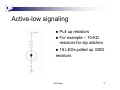
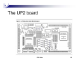
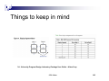
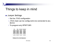
Implementation of
8-bit adder
Rashmi Kumar
8-Bit Adder
1
Administrative
This lab requires a report
Two 15-Sep-03week lab
Has a Pre-lab – so please be prepared
You will need the User Guide for the Altera
UP2 board – so please print a copy
8-Bit Adder
2
Objective of the lab
Design a 8-bit adder which is capable of:
Taking two 8-bit numbers from the DIP
switches
Display the result on the seven segment
display
Provide a visual feedback when overflow
occurs
8-Bit Adder
3
Equipment
Altera UP2 Development Board
Max-plus-II Integrated Design
Environment (Software)
8-Bit Adder
4
Suggested Design Flow
Write a Verilog code for the 8-bit adder
and the hex to seven segment display
Several ways to do this
1.
2.
Make two functional units – one for the adder,
another for the hex-to-seven segment display
Make a single unit that incorporates both addition
and conversion
Create a symbol for each block
8-Bit Adder
5
Design Flow (cont.)
Integrate your design as a top-level
design in the graphical editor
Functional Simulation – make sure that
your design is logically correct!
Major Consideration:
- All UP2 peripherals are driven active-low
8-Bit Adder
6
Active-low signaling
Pull up resistors
For example – 10-KΩ
resistors for dip witches
16 LEDs pulled up 330Ω
resistors
8-Bit Adder
7
The UP2 board
8-Bit Adder
8
Things to keep in mind
Recommended FPGA EPM7128S
LEDs are hardwired to the MAX chip
DIP switches are not – so you will need to
physically wire them (hook-up wires)
User manual has a list of pin connections
MAX_DIGIT display – seven segment display
directly connected to EPM7128S
8-Bit Adder
9
Things to keep in mind
Ref: University Program Design Laboratory Package User Guide – Altera Corp.
8-Bit Adder
10
Things to keep in mind
Jumper Settings
Set the JTAG configuration
JTAG chain can be configured to be connected to any
device
To program only EPM7128S
8-Bit Adder
11
Downloading to the chip
Functional Analysis
Verify your design ( waveform editor)
Device Selection
Pin Assignments
Compile the program
Program the Device – follow the
instructions from the User Manual
8-Bit Adder
12
Test your design!
If you programmed correctly and
transferred the design to the FPGA
successfully [ Configuration Complete] –
you should be able to feed in two 8-bit
numbers through the DIP switches, see
the sum on the 7 segment display AND
see the overflow, if it occurs
(Hint: LED or dp lights up!! or you can be innovative and
have an error message displayed on the 7 segment
display unit!!)
8-Bit Adder
13
You are all set for next week’s lab!! ☺
8-Bit Adder
14