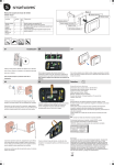
1
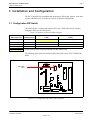
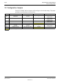
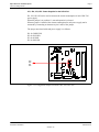
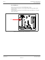
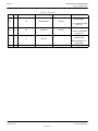
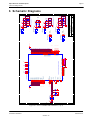
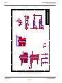
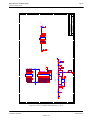
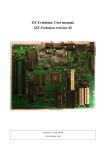
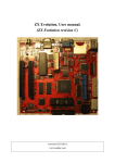
S1D13743 Mobile Graphics Engine
S5U13743P00C100 Evaluation Board
User Manual
Document Number: X70A-G-001-01
Status: Revision 1.0
Issue Date: 2007/08/15
© SEIKO EPSON CORPORATION 2007. All Rights Reserved.
Information in this document is subject to change without notice. You may download and use this document, but only for your own use in
evaluating Seiko Epson/EPSON products. You may not modify the document. Epson Research and Development, Inc. disclaims any
representation that the contents of this document are accurate or current. The Programs/Technologies described in this document may contain
material protected under U.S. and/or International Patent laws.
EPSON is a registered trademark of Seiko Epson Corporation. All other trademarks are the property of their respective owners.
Revision 1.0
Page 2
Epson Research and Development
Vancouver Design Center
S1D13743
X70A-G-001-01
S5U13743P00C100 Evaluation Board User Manual
Issue Date: 2007/08/15
Revision 1.0
Epson Research and Development
Vancouver Design Center
Page 3
Table of Contents
1
Introduction . . . . . . . . . . . . . . . . . . . . . . . . . . . . . . . . . . . . . . . . 5
2
Features . . . . . . . . . . . . . . . . . . . . . . . . . . . . . . . . . . . . . . . . . . 6
3
Installation and Configuration . . . . . . . . . . . . . . . . . . . . . . . . . . . . . . 7
3.1 Configuration DIP Switch . . . . . . . . . . . . . . . . . . . . . . . . . . . 7
3.2 Configuration Jumpers . . . . . . . . . . . . . . . . . . . . . . . . . . . . 8
4
Technical Description . . . . . . . . . . . . . . . . . . . . . . . . .
4.1 Power . . . . . . . . . . . . . . . . . . . . . . . . . .
4.1.1 Power Requirements . . . . . . . . . . . . . . . . . . . . . . . .
4.1.2 Voltage Regulators . . . . . . . . . . . . . . . . . . . . . . . . .
4.1.3 S1D13743 Power . . . . . . . . . . . . . . . . . . . . . . . . . .
4.2 Clocks . . . . . . . . . . . . . . . . . . . . . . . . . .
4.3 Reset . . . . . . . . . . . . . . . . . . . . . . . . . . .
4.4 Power Save . . . . . . . . . . . . . . . . . . . . . . . .
4.5 Host Interface . . . . . . . . . . . . . . . . . . . . . . .
4.5.1 Direct Host Bus Interface Support . . . . . . . . . . . . . . . . .
4.5.2 Connecting to the Epson S5U13U00P00C100 USB Adapter Board
4.6 LCD Panel Interface . . . . . . . . . . . . . . . . . . . . .
4.7 GPIO Connections . . . . . . . . . . . . . . . . . . . . .
5
Parts List . . . . . . . . . . . . . . . . . . . . . . . . . . . . . . . . . . . . . . . . 18
6
Schematic Diagrams . . . . . . . . . . . . . . . . . . . . . . . . . . . . . . . . . . 21
7
Board Layout . . . . . . . . . . . . . . . . . . . . . . . . . . . . . . . . . . . . . . 24
8
References . . . . . . . . . . . . . . . . . . . . . . . . . . . . . . . . . . . . . . . 26
8.1 Documents . . . . . . . . . . . . . . . . . . . . . . . . . . . . . . . 26
8.2 Document Sources . . . . . . . . . . . . . . . . . . . . . . . . . . . . 26
9
Technical Support . . . . . . . . . . . . . . . . . . . . . . . . . . . . . . . . . . . 27
9.1 EPSON Display Controllers (S1D13743) . . . . . . . . . . . . . . . . . . . . 27
9.2 Ordering Information . . . . . . . . . . . . . . . . . . . . . . . . . . . 27
S5U13743P00C100 Evaluation Board User Manual
Issue Date: 2007/08/15
.
.
.
.
.
.
.
.
.
.
.
.
.
. . . . . . .
. . . . . .
. . . . . . . .
. . . . . . . .
. . . . . . . .
. . . . . .
. . . . . .
. . . . . .
. . . . . .
. . . . . . . .
. . . . . . . .
. . . . . .
. . . . . .
12
12
12
12
12
13
13
13
14
14
15
16
17
S1D13743
X70A-G-001-01
Revision 1.0
Page 4
Epson Research and Development
Vancouver Design Center
S1D13743
X70A-G-001-01
S5U13743P00C100 Evaluation Board User Manual
Issue Date: 2007/08/15
Revision 1.0
Epson Research and Development
Vancouver Design Center
Page 5
1 Introduction
This manual describes the setup and operation of the S5U13743P00C100 Evaluation
Board. The evaluation board is designed as an evaluation platform for the S1D13743
Mobile Graphics Engine.
The S5U13743P00C100 evaluation board can be used with many native platforms via the
host connector which provides the appropriate signals to support a variety of CPUs. The
S5U13743P00C100 evaluation board can also connect to the S5U13U00P00C100 USB
Adapter board so that it can be used with a laptop or desktop computer, via USB 2.0.
This user manual is updated as appropriate. Please check the Epson Research and Development Website at www.erd.epson.com for the latest revision of this document before
beginning any development.
We appreciate your comments on our documentation. Please contact us via email at
[email protected].
S5U13743P00C100 Evaluation Board User Manual
Issue Date: 2007/08/15
S1D13743
X70A-G-001-01
Revision 1.0
Page 6
Epson Research and Development
Vancouver Design Center
2 Features
The S5U13743P00C100 Evaluation Board includes the following features:
• 121-pin FCBGA S1D13743 Mobile Graphics Engine
• Header with all S1D13743 Host Bus Interface signals
• Headers for connection to the S5U13U00P00C100 USB Adapter board
• Headers for connecting to LCD panels
• Header for S1D13743 GPIO pins (optional)
• On-board 4MHz oscillator
• 14-pin DIP socket (if a clock other than 4MHz must be used)
• 3.3V input power
• On-board voltage regulator with 1.5V output
• On-board voltage regulator with adjustable 6~24V output, 40mA max., to provide
power for LED backlight of LCD panels.
S1D13743
X70A-G-001-01
S5U13743P00C100 Evaluation Board User Manual
Issue Date: 2007/08/15
Revision 1.0
Epson Research and Development
Vancouver Design Center
Page 7
3 Installation and Configuration
The S5U13743P00C100 evaluation board incorporates a DIP switch, jumpers, and 0 ohm
resistors which allow it to be used with a variety of different configurations.
3.1 Configuration DIP Switch
The S1D13743 has 3 configuration inputs (CNF[2:0]). A DIP switch (SW1) is used to
configure CNF[2:0] as described below.
Table 3-1: Summary of Power-On/Reset Options
Power-On/Reset State
SDU13743P00C100
SW1-[4:1] Config
S1D13743
CNF[2:0] Config
1 (ON)
SW1-[1]
CNF0
Host Data lines are normal
SW1-[2]
CNF1
SW1-[3]
CNF2
SW1-[4]
-
Host Data is 16-bit
PIOVDD output current = 6.5mA
0 (OFF)
Host data lines are swapped
Host data is 8-bit
PIOVDD output current = 2.5mA
not used
= Required settings when using S5U13U00P00C100 USB Adapter board
The following figure shows the location of DIP switch SW1 on the S5U13743P00C100
board.
DIP Switch
SW1
Figure 3-1: Configuration DIP Switch (SW1) Location
S5U13743P00C100 Evaluation Board User Manual
Issue Date: 2007/08/15
S1D13743
X70A-G-001-01
Revision 1.0
Page 8
Epson Research and Development
Vancouver Design Center
3.2 Configuration Jumpers
The S5U13743P00C100 has 6 jumpers which configure various board settings. The jumper
positions for each function are shown below.
Jumper
Function
Position 1-2
Position 2-3
JP1
COREVDD
Normal
—
JP2
PLLVDD
Normal
—
JP3
IOVDD
Normal
—
JP4
IOVDD Source
H1 connector, pin 32
3.3VDD
JP5
PIOVDD
Normal
—
JP6
PIOVDD Source
H4 connector, pin 8
3.3VDD
No Jumper
COREVDD current
measurement
PLLVDD current
measurement
IOVDD current
measurement
—
PIOVDD current
measurement
—
= Required settings when using S5U13U00P00C100 USB Adapter board
S1D13743
X70A-G-001-01
S5U13743P00C100 Evaluation Board User Manual
Issue Date: 2007/08/15
Revision 1.0
Epson Research and Development
Vancouver Design Center
Page 9
JP1, JP2, JP3, JP5 - Power Supplies for the S1D13743
JP1, JP2, JP3, JP5 can be used to measure the current consumption of each S1D13743
power supply.
When the jumper is at position 1-2, normal operation is selected.
When no jumper is installed, the current consumption for each power supply can be
measured by connecting an ammeter to pin 1 and 2 of the jumper.
The jumper associated with each power supply is as follows:
JP1 for COREVDD
JP2 for PLLVDD
JP3 for IOVDD
JP5 for PIOVDD
JP3
JP5
JP1
JP2
Figure 3-2: Configuration Jumper Locations (JP1, JP2, JP3, JP5)
S5U13743P00C100 Evaluation Board User Manual
Issue Date: 2007/08/15
S1D13743
X70A-G-001-01
Revision 1.0
Page 10
Epson Research and Development
Vancouver Design Center
JP4 - IOVDD Source
JP4 is used to select the source for the IOVDD supply voltage.
When the jumper is at position 1-2, the IOVDD voltage must be provided to the H1
connector, pin 32.
When the jumper is at position 2-3, the IOVDD voltage is provided by the 3.3V power
supply of the board.
JP4
Figure 3-3: Configuration Jumper Location (JP4)
S1D13743
X70A-G-001-01
S5U13743P00C100 Evaluation Board User Manual
Issue Date: 2007/08/15
Revision 1.0
Epson Research and Development
Vancouver Design Center
Page 11
JP6 - SIOVDD Source
JP6 is used to select the source for the PIOVDD supply voltage.
When the jumper is at position 1-2, the PIOVDD voltage must be provided to the H4
connector, pin 8.
When the jumper is at position 2-3, the PIOVDD voltage is provided by the 3.3V power
supply of the board.
JP6
Figure 3-4: Configuration Jumper Location (JP6)
S5U13743P00C100 Evaluation Board User Manual
Issue Date: 2007/08/15
S1D13743
X70A-G-001-01
Revision 1.0
Page 12
Epson Research and Development
Vancouver Design Center
4 Technical Description
4.1 Power
4.1.1 Power Requirements
The S5U13743P00C100 evaluation board requires an external regulated power supply
(3.3V / 0.5A). The power is supplied to the evaluation board through pin 34 of the H1
header, or pin 5 of the P2 header.
The green LED ‘3.3V Power’ is turned on when 3.3V power is applied to the board.
4.1.2 Voltage Regulators
The S5U13743P00C100 evaluation board has an on-board linear regulator to provide the
1.5V power required by the S1D13743 Mobile Graphics Engine. It also has a step-up
switching voltage regulator to generate adjustable 6~24V, which can be used to power the
LED backlight on some LCD panels.
4.1.3 S1D13743 Power
The S1D13743 Mobile Graphics Engine requires 1.5V and 1.65~3.6V power supplies.
1.5V power for COREVDD and PLLVDD is provided by an on-board linear voltage
regulator.
IOVDD can be in the range of 1.65~3.6V. When JP4 is set to the 2-3 position, IOVDD is
connected to 3.3V. If a different voltage is required for IOVDD, set JP4 to the 1-2 position
and connect the external power supply to pin 32 of connector H1.
Note
If the IOVDD voltage is less than 3.0V, an oscillator working at the selected IOVDD
voltage must be used.
PIOVDD is the power used by the LCD interface and can be in the range of 1.65~3.6V.
When JP6 is set to the 2-3 position, PIOVDD is connected to 3.3V. If a different voltage is
needed for PIOVDD because of the LCD panel requirements, set JP6 to the 1-2 position
and connect the external power supply to pin 8 of connector H4.
S1D13743
X70A-G-001-01
S5U13743P00C100 Evaluation Board User Manual
Issue Date: 2007/08/15
Revision 1.0
Epson Research and Development
Vancouver Design Center
Page 13
4.2 Clocks
The clock for the S1D13743 Mobile Graphics Engine is provided by a 4MHz oscillator.
The S5U13743P00C100 evaluation board has a DIP14 footprint for an optional second
oscillator, Y2. This is provided for cases requiring a different clock frequency for the
S1D13743 Mobile Graphics Engine. To use Y2, an oscillator must be populated in the Y2
footprint and the following board modifications must be made.
1. Remove R10 (33 ohm resistor, size 0402) to cut the output of Y1.
2. Populate R13 with a 33 ohm resistor, size 0402, to connect the output of Y2 to the
CLKI input of the S1D13743 Mobile Graphics Engine.
Note
If the board is configured for an IOVDD voltage below 3.0V, an oscillator working at
the selected IOVDD voltage must be used at Y2. The on-board 4MHz oscillator is not
specified to work below a 3.0V supply voltage.
The S1D13743 MGE can output the input clock on the CLKOUT pin depending on the state
of the CLKOUTEN input. Both these signals are available on the H4 connector: CLKOUT
on pin 1 and CLKOUTEN on pin 4. On the board the CLKOUTEN pin is pulled down
which disables the CLKOUT signal. Note that connector H4 is not populated on the
S5U13743P00C100 evaluation board.
4.3 Reset
The S1D13743 Mobile Graphics Engine on the S5U13743P00C100 evaluation board can
be reset using a push-button (SW2), or via an active low reset signal from the host development platform (pin 33 on the H1 connector).
4.4 Power Save
The S1D13743 chip has an input called PWRSVE that will enable (when high) or disable
(when low) the power save mode. This signal is available on pin 5 of the H4 connector. On
the board the PWRSVE pin is pulled down which means power save mode is controlled
only by the S1D13743 register setting. Note that connector H4 is not populated on the
S5U13743P00C100 evaluation board.
S5U13743P00C100 Evaluation Board User Manual
Issue Date: 2007/08/15
S1D13743
X70A-G-001-01
Revision 1.0
Page 14
Epson Research and Development
Vancouver Design Center
4.5 Host Interface
4.5.1 Direct Host Bus Interface Support
All S1D13743 host interface pins are available on connector H1 which allows the
S5U13743P00C100 evaluation board to be connected to a variety of development
platforms. For detailed S1D13743 pin mapping, refer to the S1D13743 Hardware
Functional Specification, document number X70A-A-001-xx.
The following figure shows the location of host bus connector H1. H1 is a 0.1x0.1”
34-pin header (17x2).
H1
Figure 4-1: Host Bus Connector Location (H1)
For the pinout of connector H1, see “Schematic Diagrams” on page 21.
S1D13743
X70A-G-001-01
S5U13743P00C100 Evaluation Board User Manual
Issue Date: 2007/08/15
Revision 1.0
Epson Research and Development
Vancouver Design Center
Page 15
4.5.2 Connecting to the Epson S5U13U00P00C100 USB Adapter Board
The S5U13743P00C100 evaluation board is designed to connect to a S5U13U00P00C100
USB Adapter Board. The USB adapter board provides a simple connection to any computer
via a USB 2.0 connection. The S5U13743P00C100 directly connects to the USB adapter
board through connectors P1 and P2.
The USB adapter board also supplies the 3.3V power required by the S5U13743P00C100.
IOVDD should be selected for 3.3V and JP4 should be set to the 2-3 position.
When the S5U13743P00C100 is connected to the S5U13U00P00C100 USB Adapter
board, there are 2 LEDs on S5U13743P00C100 which provide a quick visual status of the
USB adapter. LED1 blinks to indicate that the USB adapter board is active. LED2 turns on
to indicate that the USB has been enumerated by the PC.
The following diagram shows the location of connectors P1 and P2. P1 and P2 are 40-pin
headers (20x2).
P1
P2
Figure 4-2: USB Adapter Connector Locations (P1 and P2)
For the pinout of connectors P1 and P2, see “Schematic Diagrams” on page 21.
Note
A windows driver must be installed on the PC when the S5U13743P00C100 is used
with the S5U13U00P00C100 USB Adapter Board. The S1D13xxxUSB driver is available at www.erd.epson.com.
S5U13743P00C100 Evaluation Board User Manual
Issue Date: 2007/08/15
S1D13743
X70A-G-001-01
Revision 1.0
Page 16
Epson Research and Development
Vancouver Design Center
4.6 LCD Panel Interface
The LCD interface signals are available on connectors H2 and H3. For S1D13743 LCD
interface pin mapping, refer to the S1D13743 Hardware Functional Specification,
document number X70A-A-001-xx.
Connector H2 is 0.1x0.1” 20-pin header (10x2) and connector H3 is 0.1x0.1” 40-pin header
(20x2). For the pinout of connectors H2 and H3, see “Schematic Diagrams” on page 21.
On the evaluation board there is an adjustable 6~24V, 40mA max. power supply. This
voltage is provided only on connector H3 (it is not used elsewhere on the board). It is
intended for use to power the LED backlight on some LCD panels. The voltage is adjusted
by the R24 pot.
Note
For LCD panels that use a CCFL backlight, an external power supply must be used to
provide power to the inverter for the CCFL backlight. Usually, the inverter current consumption is higher than the maximum 40mA current available from the on-board voltage regulator.
The following diagram shows the location of the LCD panel connectors H2 and H3.
H2
H3
Figure 4-3: LCD Panel Connectors Location (H2, H3)
For the pinout of connectors H2 and H3, see “Schematic Diagrams” on page 21.
S1D13743
X70A-G-001-01
S5U13743P00C100 Evaluation Board User Manual
Issue Date: 2007/08/15
Revision 1.0
Epson Research and Development
Vancouver Design Center
Page 17
4.7 GPIO Connections
The S1D13743 Mobile Graphics Engine has 8 GPIO pins. All the GPIO pins are routed to
the H4 connector. Note that connector H4 is not populated on the S5U13743P00C100
evaluation board.
The following figure shows the location of the GPIO connector, H4.
H4
Figure 4-4: GPIO Connector Location (H4)
For the pinout of connector H4, see “Schematic Diagrams” on page 21.
S5U13743P00C100 Evaluation Board User Manual
Issue Date: 2007/08/15
S1D13743
X70A-G-001-01
Revision 1.0
Page 18
Epson Research and Development
Vancouver Design Center
5 Parts List
Table 5-1: Parts List
Item
Qty
Reference
Part
Description
Mfg / Mfg PN / Notes
1
16
C1, C2, C3, C4, C9, C12,
C13, C14, C18, C19, C20,
C21, C26, C27, C28, C30,
C32
0.1uF
C0402
Yageo America
04022F104Z7B20D
2
12
C5, C6, C7, C8, C15, C16,
C17, C22, C23, C24, C25,
0.01uF
C0402
Yageo America
0402ZRY5V7BB103
3
1
C10
1nF
C0402
Yageo America
04022R102K9B20D
4
1
C11
10uF
C0805
Panasonic - ECG
ECJ-CV50J106M
5
1
C29
100uF 4V T
C3528
Kemet T494B107M004AS
6
2
C31, C33
0.01uF
C0402
Kemet
C0402C103K4RACTU
7
1
C34
4.7uF 10V T
C3528
Kemet T491B475K010AS
8
1
C35
10pF
C0402
Panasonic - ECG
ECJ-0EC1H100D
9
1
C36
1uF 50V
C1206
TDK C3216X7R1H105K
Panasonic - SSG
LNJ308G8LRA
10
3
D1, D2, D3
LED0603
LED GREEN SS TYPE
LOW CUR SMD
11
1
D4
MBR0530
SOD-123
Micro Commercial Co.
MBR0530-TP
TDK ACF451832-222
12
2
F1, F2
ACF451832-222
13
1
H1
HEADER_17X2
AMP 1-87215-7
14
1
H2
Extended LCD Connector
Samtec TST-110-01-G-D
15
1
H3
LCD Connector
Samtec TST-120-01-G-D
16
0
H4
HEADER 8X2
Samtec TSW-108-07-G-D
17
4
JP1, JP2, JP3, JP5
SIP2
CONN HEADER VERT
2POS .100 TIN or
GENERIC
18
2
JP4, JP6
SIP3
CONN HEADER VERT
3POS .100 TIN or
GENERIC
FILTER 3-TERM 60MHZ
300MA SMD
Steward
HZ0603B751R-10
19
2
L1, L2
Ferrite
R0603
FERRITE 200MA 938
OHMS 0603 SMD
S1D13743
X70A-G-001-01
S5U13743P00C100 Evaluation Board User Manual
Issue Date: 2007/08/15
Revision 1.0
Epson Research and Development
Vancouver Design Center
Page 19
Table 5-1: Parts List
Item
Qty
Reference
Part
Description
Mfg / Mfg PN / Notes
Panasonic - ECG
ELL-6SH100M
20
1
L3
10uH
IND_ELL6
COIL 10UH 1300MA
CHOKE SMD
21
2
P1, P2
HEADER_20X2
HDR2X20/2MM
22
23
3
R1, R2, R3
10k
R0402
3
R4, R7, R19
0
R0603
24
1
R5
150k 1%
R0402
25
5
R6, R8, R9, R11, R20
0
R0402
26
1
R10
33 1%
R0402
27
0
R12, R13
NP
R0402
28
3
R14, R15, R16
270 1%
R0402
29
3
R17, R18, R23
47k
R0402
30
1
R21
887k 1%
RC0603
31
1
R22
22k
R0402
32
1
R24
200k
6
SH1, SH2, SH3, SH4,
SH5, SH6
33
.100 in. Jumper Shunt
3M 151240-8422-RB
Panasonic - ECG
EVN-5ESX50B25
Not Applicable
Sullins Electronics Corp.
STC02SYAN
JUMPER SHORTING TIN
CTS Corp 218-4LPST
34
1
SW1
SW4_DIPSW4
DIPSW4
SWITCH DIP HALF
PITCH 4POS
ITT Industries
KSC241GLFS
35
1
SW2
SW TACT-SPST
SW_EVQQW
SWITCH TACT SILVER
PLT GULLWING
Keystone 5015
36
2
TPGND1, TP3.3VDD1
TP_SMT
TP_1206
37
0
TP1, TP2, TP3, TP4
T POINT F
SIP1
38
1
U1
S1D13743
S5U13743P00C100 Evaluation Board User Manual
Issue Date: 2007/08/15
PC TEST POINT
MINIATURE SMT
S1D13743
X70A-G-001-01
Revision 1.0
Page 20
Epson Research and Development
Vancouver Design Center
Table 5-1: Parts List
Item
Qty
Reference
Part
Description
Mfg / Mfg PN / Notes
Texas Instruments
TPS76915DBVT
39
1
U2
TPS76915DBVT
SOT23-5
IC 1.5V 100MA LDO REG
SOT-23-5
TI TPS61040DVBR
40
1
U3
TPS61040
SOT23-5
IC CONV DC/DC BOOST
LP SOT-23-5
Connor-Winfield
CWX823-4.0M
41
1
Y1
4M OSC
OSC 4.0000MHz 3.3V
50ppm SMD
42
0
Y2
14-Pin DIP
S1D13743
X70A-G-001-01
AMP 2-641609-1
S5U13743P00C100 Evaluation Board User Manual
Issue Date: 2007/08/15
Revision 1.0
A
B
C
IOVDD
SW1
4
3
2
1
SW4_DIPSW4
5
6
7
8
R1
10k
5
R2
10k
2
R3
10k
MD[15:0]
3
2
3
3
2
2
2
2
2
2
2
PWRSVE
CLKI
CLKOUT
CLKOUTEN
WE#
RD#
CS#
D/C#
TE
GPIO_INT
RESET#
MD0
MD1
MD2
MD3
MD4
MD5
MD6
MD7
MD8
MD9
MD10
MD11
MD12
MD13
MD14
MD15
F2
D5
F1
E1
E2
J3
E3
H3
G3
F3
A4
A3
B4
C8
C9
C7
C10
D2
D3
D1
C1
C3
B2
A5
A6
A7
A8
A9
B8
B9
B10
C2
B3
B5
B6
B7
U1
SCANEN
VCP
TEST0
TEST1
TEST2
PWRSVE
TESTEN
CNF2
CNF1
CNF0
CLKI
CLKOUT
CLKOUTEN
W E#
RD#
CS#
D/C#
TE
GPIO_INT
RESET#
MD0
MD1
MD2
MD3
MD4
MD5
MD6
MD7
MD8
MD9
MD10
MD11
MD12
MD13
MD14
MD15
4
IO
PIO
PLL
The pin names enclosed in brackets applies to S1D13743 only.
S1D13742 (S1D13743)
CORE
D7
E4
G7
H6
CoreVDD
CoreVDD
CoreVDD
CoreVDD
C4
D8
H4
IOVDD
IOVDD
IOVDD
4
PIOVDD
PIOVDD
PIOVDD
PIOVDD
D4
PLLVDD
E8
G4
H5
H7
PLLVSS
D6
NC
NC
NC
NC
NC
NC
NC
NC
NC
NC
NC
NC
NC
A1
A2
A10
A11
B1
B11
E9
K1
K11
L1
L2
L10
L11
Revision 1.0
3
VSS
VSS
VSS
VSS
VSS
VSS
VSS
VSS
VSS
VSS
VSS
S5U13743P00C100 Evaluation Board User Manual
Issue Date: 2007/08/15
3
G6
G5
F7
F6
F5
F4
E7
E6
E5
C6
C5
D
5
GPIO7
GPIO6
GPIO5
GPIO4
GPIO3
GPIO2
GPIO1
GPIO0
VD0
VD1
VD2
VD3
VD4
VD5
VD6
VD7
VD8
VD9
VD10
VD11
VD12
VD13
VD14
VD15
VD16
VD17
VD18
VD19
VD20
VD21
VD22
VD23
VD24 (NC)
VD25 (NC)
VD26 (NC)
VD27 (NC)
VD28 (NC)
VD29 (NC)
VD30 (NC)
VD31 (NC)
VD32 (NC)
VD33 (NC)
VD34 (NC)
VD35 (NC)
VS
HS
PCLK
DE
K3
K2
J2
J1
H2
H1
G2
G1
L9
L8
L7
L6
L5
L4
L3
K10
K9
K8
K7
K6
K5
K4
J11
J10
J9
J8
J7
J6
J5
J4
H11
H10
H9
H8
G11
G10
G9
G8
F11
F10
F9
F8
E11
E10
D10
D9
D11
C11
GPIO7
GPIO6
GPIO5
GPIO4
GPIO3
GPIO2
GPIO1
GPIO0
VS
HS
PCLK
DE
VD0
VD1
VD2
VD3
VD4
VD5
VD6
VD7
VD8
VD9
VD10
VD11
VD12
VD13
VD14
VD15
VD16
VD17
VD18
VD19
VD20
VD21
VD22
VD23
VD24
VD25
VD26
VD27
VD28
VD29
VD30
VD31
VD32
VD33
VD34
VD35
3
3
3
3
3
3
3
3
3
3
3
3
VD[35:0]
3
2
2
Date:
Size
B
Title
PIOVDD SOURCE
3
2
1
.100 in. Jumper Shunt
SH6
JP6
IOVDD SOURCE
3
2
1
.100 in. Jumper Shunt
SH4
JP4
0.01uF
C8
C16
0.01uF
0.01uF
0.1uF
C15
C13
0.1uF
IO
C12
0.01uF
C17
0.1uF
C14
C11
10uF
PIOVDD
0.01uF
C22
0.1uF
C18
PIO
0.01uF
C23
0.1uF
C19
0.01uF
C24
0.1uF
C20
1
Sheet
1
of
3
Rev
1.0
0.01uF
C25
0.1uF
C21
Place a 0.01uF and a 0.1uF cap on each PIOVDD
power pins of the S1D13742/S1D13743
Saturday, June 09, 2007
Document Number
<Doc>
C10
1nF
L1
PLL
Ferrite
L2
Ferrite
0.1uF
C9
S1D13742/S1D13743 PFBGA121
3.3VDD
PIOVDD
PIOVDD_IN
PIOVDD
2
1
0.01uF
0.01uF
0.1uF
C4
Place a 0.01uF and a 0.1uF cap on each IOVDD
power pins of the S1D13742/S1D13743
.100 in. Jumper Shunt
SH5
JP5
3.3VDD
IOVDD
IOVDD_IN
IOVDD
2
1
.100 in. Jumper Shunt
SH3
JP3
PLLVDD
IOVDD
.100 in. Jumper Shunt
1.5VDD
SH2
JP2
2
1
C7
C6
C5
0.01uF
0.1uF
0.1uF
0.1uF
C3
C2
C1
CORE
1
Place a 0.01uF and a 0.1uF cap on each COREVDD
power pin of the S1D13742/S1D743
COREVDD
2
1
.100 in. Jumper Shunt
SH1
1.5VDD
JP1
A
B
C
D
Epson Research and Development
Vancouver Design Center
Page 21
6 Schematic Diagrams
Figure 6-1: S5U13743P00C100 Schematics (1 of 3)
S1D13743
X70A-G-001-01
A
B
C
5
0
D/C#
CS#
R14
270 1%
HEARTBEAT
3.3VDD
TP3.3VDD1
TP_SMT
R4
IOVDD
0
0
D1
LED1
R11
1
3
5
7
9
11
13
15
17
19
21
23
25
27
29
31
33
35
37
39
R15
270 1%
ENUMERATED
0
HEARTBEAT
R8
R7
MD6
MD4
MD2
MD0
MD15
MD13
MD11
MD9
RD#
GPIO_INT
1
3
5
7
9
11
13
15
17
19
21
23
25
27
29
31
33
35
37
39
2
4
6
8
10
12
14
16
18
20
22
24
26
28
30
32
34
36
38
40
2
4
6
8
10
12
14
16
18
20
22
24
26
28
30
32
34
36
38
40
D2
LED2
R16
270 1%
HEADER_20X2
P2
HEADER_20X2
P1
4
D3
3.3V Power
3.3VDD
ENUMERATED
MD14
MD12
MD10
MD8
MD7
MD5
MD3
MD1
WE#
1
1
1
1
1
1
1
CS#
WE#
RD#
D/C#
GPIO_INT
TE
RESET#
1
D
4
TPGND1
TP_SMT
TP3
CS#
WE#
RD#
D/C#
GPIO_INT
MD8
MD10
MD12
MD14
MD0
MD2
MD4
MD6
1
3
5
7
9
11
13
15
17
19
21
23
25
27
29
31
33
2
4
6
8
10
12
14
16
18
20
22
24
26
28
30
32
34
3
HEADER_17X2
H1
3
IOVDD_IN
3.3VDD
MD9
MD11
MD13
MD15
MD1
MD3
MD5
MD7
MD[15:0]
1
0.01uF
0.1uF
2
C33
0.01uF
C31
R6
C32
IOVDD
0.1uF
C30
R9
0
3.3VDD
0.1uF
C27
3.3VDD
2
0
3
1
GND
/EN
Vin
GND
Date:
Size
B
OUT
OE
NP
3
1
8
1
4
R13
R10
NP
+
TP1
33 1%
0.1uF
C28
RESET#
Saturday, June 09, 2007
Document Number
<Doc>
1
TP2
1
2
CLKI
1.5VDD
C29
100uF 4V T
1
Sheet
Host connectors / 1.5V power / clock / reset
TTL/CMOS
Oscillator
Title
OE
OUT
14-Pin DIP
GND
VDD
Y2
R12
4M OSC
7
NC/FB
5
0.1uF
C26
Vout
TPS76915DBVT
VDD
Y1
14
2
4
2
3
1
U2
SW TACT-SPST
4
2
SW2
R5
150k 1%
IOVDD
1
2
5
A
K
A
K
Revision 1.0
A
S1D13743
X70A-G-001-01
K
of
3
Rev
1.0
1
A
B
C
D
Page 22
Epson Research and Development
Vancouver Design Center
Figure 6-2: S5U13743P00C100 Schematics (2 of 3)
S5U13743P00C100 Evaluation Board User Manual
Issue Date: 2007/08/15
1
A
B
C
R19
3.3VDD
0
5
C34
1
4.7uF 10V T
3
F1
ACF451832-222
1
2
D
1
2
+
1
1
1
1
R20
0
PCLK
DE
HS
VS
4
5
U3
FB
SW
TPS61040
EN GND
VIN
L3
10uH
2
3
1
2
4
6
8
10
12
14
16
18
20
H3
2
4
6
8
10
12
14
16
18
20
22
24
26
28
30
32
34
36
38
40
4
A
R24
200k
R23
47k
R21
887k 1%
K
D4
MBR0530
LCD Connector
1
3
5
7
9
11
13
15
17
19
21
23
25
27
29
31
33
35
37
39
Internal Step Up 6 to 24V
Power Supply
Typical 12V @ 40mA
VD17
VD16
VD15
VD11
VD10
VD9
VD5
VD4
VD3
VD14
VD13
VD12
VD8
VD7
VD6
VD2
H2
Extended LCD Connector
1
3
5
7
9
11
13
15
17
19
Vout=1.233x[1+R103/(R105+R106)] (V)
VD[35:0]
VD26
VD28
VD30
VD32
VD34
VD18
VD20
VD22
VD24
4
1
Revision 1.0
3
S5U13743P00C100 Evaluation Board User Manual
Issue Date: 2007/08/15
2
VD1
VD0
VD27
VD29
VD31
VD33
VD35
VD19
VD21
VD23
VD25
C35
10pF
C36
1uF 50V
1
3
F2
ACF451832-222
PIOVDD
12VDD
2
5
R22
22k
12VDD
TP4
3
3
1
PWRSVE
R17
47k
1
1
1
1
1
GPIO0
GPIO2
GPIO4
GPIO6
CLKOUT
IOVDD
2
1
3
5
7
9
11
13
15
2
2
4
6
8
10
12
14
16
HEADER 8X2
H4
Date:
Size
B
Title
1
1
1
1
R18
47k
Saturday, June 09, 2007
Document Number
<Doc>
LCD Connectors/ GPIO connector
PIOVDD_IN
GPIO1
GPIO3
GPIO5
GPIO7
1
Sheet
CLKOUTEN
1
1
3
of
3
Rev
1.0
A
B
C
D
Epson Research and Development
Vancouver Design Center
Page 23
Figure 6-3: S5U13743P00C100 Schematics (3 of 3)
S1D13743
X70A-G-001-01
Page 24
Epson Research and Development
Vancouver Design Center
7 Board Layout
Figure 7-1: S5U13743P00C100 Board Layout - Top View
S1D13743
X70A-G-001-01
S5U13743P00C100 Evaluation Board User Manual
Issue Date: 2007/08/15
Revision 1.0
Epson Research and Development
Vancouver Design Center
Page 25
Figure 7-2: S5U13743P00C100 Board Layout - Bottom View
S5U13743P00C100 Evaluation Board User Manual
Issue Date: 2007/08/15
S1D13743
X70A-G-001-01
Revision 1.0
Page 26
Epson Research and Development
Vancouver Design Center
8 References
8.1 Documents
• Epson Research and Development, Inc., S1D13743 Hardware Functional Specification,
document number X70A-A-001-xx.
8.2 Document Sources
• Epson Research and Development Website: http://www.erd.epson.com.
S1D13743
X70A-G-001-01
S5U13743P00C100 Evaluation Board User Manual
Issue Date: 2007/08/15
Revision 1.0
Epson Research and Development
Vancouver Design Center
Page 27
9 Technical Support
9.1 EPSON Display Controllers (S1D13743)
Japan
Seiko Epson Corporation
IC International Sales Group
421-8, Hino, Hino-shi
Tokyo 191-8501, Japan
Tel: 042-587-5812
Fax: 042-587-5564
http://www.epson.co.jp/
North America
Epson Electronics America, Inc.
2580 Orchard Parkway
San Jose, CA 95131, USA
Tel: (408) 922-0200
Fax: (408) 922-0238
http://www.eea.epson.com/
Taiwan
Epson Taiwan Technology & Trading Ltd.
14F, No. 7
Song Ren Road
Taipei 110, Taiwan, ROC
Tel: 02-8786-6688
Fax: 02-8786-6677
http://www.epson.com.tw/
Hong Kong
Epson Hong Kong Ltd.
20/F., Harbour Centre
25 Harbour Road
Wanchai, Hong Kong
Tel: 2585-4600
Fax: 2827-4346
http://www.epson.com.hk/
Europe
Epson Europe Electronics GmbH
Riesstrasse 15
80992 Munich, Germany
Tel: 089-14005-0
Fax: 089-14005-110
http://www.epson-electronics.de/
Singapore
Epson Singapore Pte Ltd
1 HarbourFront Place #03-02
HarbourFront Tower One
Singapore, 098633
Tel: (65) 6586-5500
Fax: (65) 6271-3182
http://www.epson.com.sg/
9.2 Ordering Information
To order the S5U13743P00C100 Evaluation Board, contact the Epson sales representative
in your area and order part number S5U13743P00C100.
S5U13743P00C100 Evaluation Board User Manual
Issue Date: 2007/08/15
S1D13743
X70A-G-001-01
Revision 1.0
Page 28
Epson Research and Development
Vancouver Design Center
Change Record
X70A-G-001-01
Revision 1.0 - Issued: August 15, 2007
• created from X63A-G-002-01
• updated for the S1D13743
S1D13743
X70A-G-001-01
S5U13743P00C100 Evaluation Board User Manual
Issue Date: 2007/08/15
Revision 1.0
Mouser Electronics
Authorized Distributor
Click to View Pricing, Inventory, Delivery & Lifecycle Information:
Epson:
S5U13743P00C100