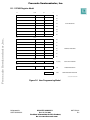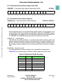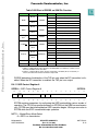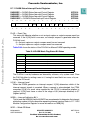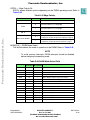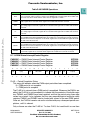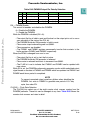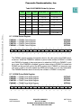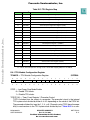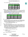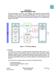
1
Freescale Semiconductor, Inc.
APPENDIX D
REGISTER SUMMARY
This appendix contains address maps, register diagrams, and bit/field definitions for
MC68336 and MC68376 microcontrollers. More detailed information about register
function is provided in the appropriate sections of the manual.
Freescale Semiconductor, Inc...
Except for central processing unit resources, information is presented in the intermodule bus address order shown in Table D-1.
Table D-1 Module Address Map
Module
Size
(Bytes)
Base
Address
SIM
128
$YFFA00
SRAM
8
$YFFB40
MRM (MC68376 Only)
32
$YFF820
QADC
512
$YFF200
QSM
512
$YFFC00
CTM4
256
$YFF400
TPU
512
$YFFE00
TPURAM
64
$YFFB00
TouCAN (MC68376 Only)
384
$YFF080
Control registers for all the modules in the microcontroller are mapped into a 4-Kbyte
block. The state of the module mapping (MM) bit in the SIM configuration register
(SIMCR) determines where the control register block is located in the system memory
map. When MM = 0, register addresses range from $7FF000 to $7FFFFF; when MM
= 1, register addresses range from $FFF000 to $FFFFFF.
In the module memory maps in this appendix, the “Access” column specifies which
registers are accessible when the CPU32 is in supervisor mode only and which registers can be assigned to either supervisor or user mode.
D.1 Central Processor Unit
CPU32 registers are not part of the module address map. Figure D-1 and Figure D-2
show a functional representation of CPU32 resources.
MC68336/376
USER’S MANUAL
REGISTER SUMMARY
Rev. 15 Oct 2000
For More Information On This Product,
Go to: www.freescale.com
MOTOROLA
D-1
Freescale Semiconductor, Inc.
D.1.1 CPU32 Register Model
31
16 15
8 7
0
D0
D1
D2
D3
DATA REGISTERS
D4
D5
D6
Freescale Semiconductor, Inc...
D7
31
16 15
0
A0
A1
A2
A3
ADDRESS REGISTERS
A4
A5
A6
31
16 15
0
A7 (SSP)
31
USER STACK POINTER
0
PC
7
PROGRAM COUNTER
0
CCR
CONDITION CODE REGISTER
CPU32 USER PROG MODEL
Figure D-1 User Programming Model
MC68336/376
USER’S MANUAL
REGISTER SUMMARY
Rev. 15 Oct 2000
For More Information On This Product,
Go to: www.freescale.com
MOTOROLA
D-2
Freescale Semiconductor, Inc.
31
16 15
0
A7’ (SSP)
15
8 7
SUPERVISOR STACK POINTER
0
(CCR)
31
STATUS REGISTER
SR
0
VBR
VECTOR BASE REGISTER
SFC
ALTERNATE FUNCTION
DFC
CODE REGISTERS
0
2
Freescale Semiconductor, Inc...
CPU32 SUPV PROG MODEL
Figure D-2 Supervisor Programming Model Supplement
D.1.2 Status Register
SR — Status Register
15
14
T[1:0]
13
12
11
S
0
0
1
0
0
10
9
8
IP[2:0]
7
6
5
4
3
2
1
0
0
0
0
X
N
Z
V
C
0
0
0
U
U
U
U
U
RESET:
0
0
1
1
1
The status register (SR) contains condition codes, an interrupt priority mask, and three
control bits. The condition codes are contained in the condition code register (CCR),
the lower byte of the SR. (The lower and upper bytes of the status register are also
referred to as the user and system bytes, respectively.) In user mode, only the CCR is
available. In supervisor mode, software can access the full status register.
T[1:0] — Trace Enable
This field places the processor in one of two tracing modes or disables tracing. Refer
to Table D-2.
Table D-2 T[1:0] Encoding
T[1:0]
Response
00
No tracing
01
Trace on change of flow
10
Trace on instruction execution
11
Undefined; reserved
S — Supervisor/User State
0 = CPU operates at user privilege level
1 = CPU operates at supervisor privilege level
IP[2:0] — Interrupt Priority Mask
MC68336/376
USER’S MANUAL
REGISTER SUMMARY
Rev. 15 Oct 2000
For More Information On This Product,
Go to: www.freescale.com
MOTOROLA
D-3
Freescale Semiconductor, Inc.
The priority value in this field (0 to 7) is used to mask interrupts.
X — Extend Flag
Used in multiple-precision arithmetic operations. In many instructions, it is set to the
same value as the C bit.
N — Negative Flag
Set when the MSB of a result register is set.
Z — Zero Flag
Set when all bits of a result register are zero.
Freescale Semiconductor, Inc...
V — Overflow Flag
Set when two's complement overflow occurs as the result of an operation.
C — Carry Flag
Set when a carry or borrow occurs during an arithmetic operation. Also used during
shift and rotate instructions to facilitate multiple word operations.
D.2 System Integration Module
Table D-3 shows the SIM address map. The column labeled “Access” indicates the
privilege level at which the CPU32 must be operating to access the register. A
designation of “S” indicates that supervisor mode is required. A designation of “S/U”
indicates that the register can be programmed for either supervisor mode access or
unrestricted access.
Table D-3 SIM Address Map
Access
Address1
S
$YFFA00
15
8
7
0
SIM Module Configuration Register (SIMCR)
S
$YFFA02
SIM Test Register (SIMTR)
S
$YFFA04
Clock Synthesizer Control Register (SYNCR)
S
$YFFA06
S
$YFFA08
Not Used
Reset Status Register (RSR)
SIM Test Register E (SIMTRE)
S
$YFFA0A
Not Used
S
$YFFA0C
Not Used
S
$YFFA0E
Not Used
S/U
$YFFA10
Not Used
S/U
$YFFA12
Not Used
Port E Data (PORTE1)
S/U
$YFFA14
Not Used
Port E Data Direction (DDRE)
S
$YFFA16
Not Used
Port E Pin Assignment (PEPAR)
S/U
$YFFA18
Not Used
Port F Data (PORTF0)
Port E Data (PORTE0)
S/U
$YFFA1A
Not Used
Port F Data (PORTF1)
S/U
$YFFA1C
Not Used
Port F Data Direction (DDRF)
S
$YFFA1E
Not Used
Port F Pin Assignment (PFPAR)
S
$YFFA20
Not Used
System Protection Control (SYPCR)
S
$YFFA22
MC68336/376
USER’S MANUAL
Periodic Interrupt Control Register (PICR)
REGISTER SUMMARY
Rev. 15 Oct 2000
For More Information On This Product,
Go to: www.freescale.com
MOTOROLA
D-4
Freescale Semiconductor, Inc.
Freescale Semiconductor, Inc...
Table D-3 SIM Address Map (Continued)
Access
Address1
S
$YFFA24
15
8
7
0
Periodic Interrupt Timing Register (PITR)
S
$YFFA26
S
$YFFA28
Not Used
Not Used
S
$YFFA2A
Not Used
S
$YFFA2C
Not Used
S
$YFFA2E
Not Used
S
$YFFA30
Test Module Master Shift A (TSTMSRA)
S
$YFFA32
Test Module Master Shift B (TSTMSRB)
S
$YFFA34
Test Module Shift Count (TSTSC)
S
$YFFA36
Test Module Repetition Counter (TSTRC)
S
$YFFA38
Test Module Control (CREG)
S/U
$YFFA3A
Test Module Distributed (DREG)
$YFFA3C
Not Used
$YFFA3E
S/U
$YFFA40
Software Service (SWSR)
Not Used
Not Used
Port C Data (PORTC)
$YFFA42
Not Used
$YFFA44
Chip-Select Pin Assignment (CSPAR0)
S
$YFFA46
Chip-Select Pin Assignment (CSPAR1)
S
$YFFA48
Chip-Select Base Boot (CSBARBT)
S
$YFFA4A
Chip-Select Option Boot (CSORBT)
S
$YFFA4C
Chip-Select Base 0 (CSBAR0)
S
$YFFA4E
Chip-Select Option 0 (CSOR0)
S
$YFFA50
Chip-Select Base 1 (CSBAR1)
S
$YFFA52
Chip-Select Option 1 (CSOR1)
S
$YFFA54
Chip-Select Base 2 (CSBAR2)
S
$YFFA56
Chip-Select Option 2 (CSOR2)
S
$YFFA58
Chip-Select Base 3 (CSBAR3)
S
$YFFA5A
Chip-Select Option 3 (CSOR3)
S
$YFFA5C
Chip-Select Base 4 (CSBAR4)
S
$YFFA5E
Chip-Select Option 4 (CSOR4)
S
$YFFA60
Chip-Select Base 5 (CSBAR5)
S
$YFFA62
Chip-Select Option 5 (CSOR5)
S
$YFFA64
Chip-Select Base 6 (CSBAR6)
S
$YFFA66
Chip-Select Option 6 (CSOR6)
S
$YFFA68
Chip-Select Base 7 (CSBAR7)
S
$YFFA6A
Chip-Select Option 7 (CSOR7)
S
$YFFA6C
Chip-Select Base 8 (CSBAR8)
S
$YFFA6E
Chip-Select Option 8 (CSOR8)
S
$YFFA70
Chip-Select Base 9 (CSBAR9)
S
$YFFA72
Chip-Select Option 9 (CSOR9)
S
$YFFA74
Chip-Select Base 10 (CSBAR10)
S
$YFFA76
Chip-Select Option 10 (CSOR10)
S
MC68336/376
USER’S MANUAL
REGISTER SUMMARY
Rev. 15 Oct 2000
For More Information On This Product,
Go to: www.freescale.com
MOTOROLA
D-5
Freescale Semiconductor, Inc.
Table D-3 SIM Address Map (Continued)
Address1
Access
15
8
7
$YFFA78
Not Used
$YFFA7A
Not Used
$YFFA7C
Not Used
$YFFA7E
Not Used
0
NOTES:
1. Y = M111, where M is the logic state of the module mapping (MM) bit in the SIMCR.
D.2.1 SIM Configuration Register
Freescale Semiconductor, Inc...
SIMCR — SIM Configuration Register
$TFFA00
15
14
13
12
11
10
9
EXOFF
FRZS
W
FRZB
M
8
0
RSVD1
0
SHEN[1:0]
0
0
DATA11
0
0
7
6
5
4
SUPV
MM
0
0
1
1
0
0
3
2
1
0
IARB[3:0]
RESET:
0
0
0
1
1
1
1
NOTES:
1. This bit must be left at zero. Pulling DATA11 high during reset ensures this bit remains zero. A one in this bit
could allow the MCU to enter an unsupported operating mode.
SIMCR controls system configuration. SIMCR can be read or written at any time, except for the module mapping (MM) bit, which can only be written once.
EXOFF — External Clock Off
0 = The CLKOUT pin is driven during normal operation.
1 = The CLKOUT pin is placed in a high-impedance state.
FRZSW — Freeze Software Enable
0 = When FREEZE is asserted, the software watchdog and periodic interrupt timer
counters continue to run.
1 = When FREEZE is asserted, the software watchdog and periodic interrupt timer
counters are disabled, preventing interrupts during background debug mode.
FRZBM — Freeze Bus Monitor Enable
0 = When FREEZE is asserted, the bus monitor continues to operate.
1 = When FREEZE is asserted, the bus monitor is disabled.
SHEN[1:0] — Show Cycle Enable
The SHEN field determines how the external bus is driven during internal transfer
operations. A show cycle allows internal transfers to be monitored externally.
Table D-4 shows whether show cycle data is driven externally, and whether external
bus arbitration can occur. To prevent bus conflict, external peripherals must not be enabled during show cycles.
MC68336/376
USER’S MANUAL
REGISTER SUMMARY
Rev. 15 Oct 2000
For More Information On This Product,
Go to: www.freescale.com
MOTOROLA
D-6
Freescale Semiconductor, Inc.
Table D-4 Show Cycle Enable Bits
Freescale Semiconductor, Inc...
SHEN[1:0]
Action
00
Show cycles disabled, external arbitration enabled
01
Show cycles enabled, external arbitration disabled
10
Show cycles enabled, external arbitration enabled
11
Show cycles enabled, external arbitration enabled;
internal activity is halted by a bus grant
SUPV — Supervisor/Unrestricted Data Space
The SUPV bit places the SIM global registers in either supervisor or user data space.
0 = Registers with access controlled by the SUPV bit are accessible in either
supervisor or user mode.
1 = Registers with access controlled by the SUPV bit are restricted to supervisor
access only.
MM — Module Mapping
0 = Internal modules are addressed from $7FF000 – $7FFFFF.
1 = Internal modules are addressed from $FFF000 – $FFFFFF.
IARB[3:0] — Interrupt Arbitration ID
Each module that can generate interrupts, including the SIM, has an IARB field. Each
IARB field can be assigned a value from $0 to $F. During an interrupt acknowledge
cycle, IARB permits arbitration among simultaneous interrupts of the same priority level. The reset value of the SIM IARB field is $F. This prevents SIM interrupts from being
discarded during system initialization.
D.2.2 System Integration Test Register
SIMTR — System Integration Test Register
Used for factory test only.
$YFFA02
D.2.3 Clock Synthesizer Control Register
SYNCR — Clock Synthesizer Control Register
15
W
14
13
12
11
X
10
9
8
Y[5:0]
7
$YFFA04
6
5
4
EDIV
0
0
RSVD1
0
0
0
0
3
2
SLOC RSVD
1
K
1
0
STSI
M
STEX
T
0
0
RESET:
0
0
1
1
1
1
1
1
U
0
NOTES:
1. Ensure that initialization software does not change the value of these bits. They should always be zero.
SYNCR determines system clock operating frequency and operation during low-power
stop mode. Clock frequency is determined by SYNCR bit settings as follows:
MC68336/376
USER’S MANUAL
REGISTER SUMMARY
Rev. 15 Oct 2000
For More Information On This Product,
Go to: www.freescale.com
MOTOROLA
D-7
Freescale Semiconductor, Inc.
fref
( 2W + X )
f sys = ---------- [ 4 ( Y + 1 ) ( 2
)]
128
W — Frequency Control (VCO)
This bit controls a prescaler tap in the synthesizer feedback loop. Setting this bit
increases the VCO speed by a factor of four. VCO relock delay is required.
Freescale Semiconductor, Inc...
X — Frequency Control (Prescaler)
This bit controls a divide by two prescaler that is not in the synthesizer feedback loop.
Setting the bit doubles clock speed without changing the VCO speed. No VCO relock
delay is required.
Y[5:0] — Frequency Control (Counter)
The Y field controls the modulus down counter in the synthesizer feedback loop, causing it to divide by a value of Y + 1. VCO relock delay is required.
EDIV — E Clock Divide Rate
0 = ECLK frequency is system clock divided by 8.
1 = ECLK frequency is system clock divided by 16.
ECLK is an external M6800 bus clock available on ADDR23.
SLOCK — Synthesizer Lock Flag
0 = VCO is enabled, but has not locked.
1 = VCO has locked on the desired frequency or VCO is disabled.
The MCU remains in reset until the synthesizer locks, but SLOCK does not indicate
synthesizer lock status until after the user writes to SYNCR.
STSIM — Stop Mode SIM Clock
0 = When LPSTOP is executed, the SIM clock is driven from the crystal oscillator
and the VCO is turned off to conserve power.
1 = When LPSTOP is executed, the SIM clock is driven from the VCO.
STEXT — Stop Mode External Clock
0 = When LPSTOP is executed, the CLKOUT signal is held negated to conserve
power.
1 = When LPSTOP is executed and EXOFF ¦ 1 in SIMCR, the CLKOUT signal is
driven from the SIM clock, as determined by the state of the STSIM bit.
D.2.4 Reset Status Register
RSR — Reset Status Register
15
$YFFA07
8
NOT USED
7
6
5
4
3
2
1
0
EXT
POW
SW
HLT
0
RSVD
SYS
TST
RSR contains a status bit for each reset source in the MCU. RSR is updated when the
MCU comes out of reset. A set bit indicates what type of reset occurred. If multiple
sources assert reset signals at the same time, more than one bit in RSR may be set.
This register can be read at any time; writes have no effect.
MC68336/376
USER’S MANUAL
REGISTER SUMMARY
Rev. 15 Oct 2000
For More Information On This Product,
Go to: www.freescale.com
MOTOROLA
D-8
Freescale Semiconductor, Inc.
EXT — External Reset
Reset caused by the RESET pin.
POW — Power-Up Reset
Reset caused by the power-up reset circuit.
SW — Software Watchdog Reset
Reset caused by the software watchdog circuit.
HLT — Halt Monitor Reset
Reset caused by the halt monitor.
Freescale Semiconductor, Inc...
SYS — System Reset
Reset caused by a RESET instruction.
TST — Test Submodule Reset
Reset caused by the test submodule. Used during system test only.
D.2.5 System Integration Test Register (ECLK)
SIMTRE — System Integration Test Register (ECLK)
Used for factory test only.
$YFFA08
D.2.6 Port E Data Register
PORTE0 — Port E0 Data Register
PORTE1 — Port E1 Data Register
15
$YFFA11
$YFFA13
8
NOT USED
7
6
5
4
3
2
1
0
PE7
PE6
PE5
PE4
PE3
PE2
PE1
PE0
U
U
U
U
U
U
U
U
RESET:
PORTE is an internal data latch that can be accessed at two locations. It can be read
or written at any time. If a port E I/O pin is configured as an output, the corresponding
bit value is driven out on the pin. When a pin is configured as an output, a read of
PORTE returns the latched bit value; when a pin is configured as an input, a read
returns the pin logic level.
D.2.7 Port E Data Direction Register
DDRE — Port E Data Direction Register
15
$YFFA15
8
NOT USED
7
6
5
DDE7 DDE6 DDE5
4
3
2
1
0
DDE4
DDE3
DDE2
DDE1
DDE0
0
0
0
0
0
RESET:
0
0
0
Bits in this register control the direction of the port E pin drivers when pins are configured for I/O. Setting a bit configures the corresponding pin as an output; clearing a bit
MC68336/376
USER’S MANUAL
REGISTER SUMMARY
Rev. 15 Oct 2000
For More Information On This Product,
Go to: www.freescale.com
MOTOROLA
D-9
Freescale Semiconductor, Inc.
configures the corresponding pin as an input. This register can be read or written at
any time.
D.2.8 Port E Pin Assignment Register
PEPAR — Port E Pin Assignment
$YFFA17
15
8
NOT USED
7
6
5
4
3
2
1
0
PEPA PEPA PEPA PEPA PEPA
7
6
5
4
3
PEPA
2
PEPA
1
PEPA
0
DATA DATA DATA DATA DATA
8
8
8
8
8
DATA
8
DATA
8
DATA
8
Freescale Semiconductor, Inc...
RESET:
Bits in this register determine the function of port E pins. Setting a bit assigns the corresponding pin to a bus control signal; clearing a bit assigns the pin to I/O port E. Refer
to Table D-5.
Table D-5 Port E Pin Assignments
PEPAR Bit
Port E Signal
Bus Control Signal
PEPA7
PE7
SIZ1
PEPA6
PE6
SIZ0
PEPA5
PE5
AS
PEPA4
PE4
DS
PEPA3
PE3
RMC
PEPA2
PE2
AVEC
PEPA1
PE1
DSACK1
PEPA0
PE0
DSACK0
D.2.9 Port F Data Register
PORTF0— Port F Data Register 0
PORTF1— Port F Data Register 1
15
$YFFA19
$YFFA1B
8
NOT USED
7
6
5
4
3
2
1
0
PF7
PF6
PF5
PF4
PF3
PF2
PF1
PF0
U
U
U
U
U
U
U
U
RESET:
PORTF is an internal data latch that can be accessed at two locations. It can be read
or written at any time. If a port F I/O pin is configured as an output, the corresponding
bit value is driven out on the pin. When a pin is configured as an output, a read of
PORTF returns the latched bit value; when a pin is configured as an input, a read
returns the pin logic level.
MC68336/376
USER’S MANUAL
REGISTER SUMMARY
Rev. 15 Oct 2000
For More Information On This Product,
Go to: www.freescale.com
MOTOROLA
D-10
Freescale Semiconductor, Inc.
D.2.10 Port F Data Direction Register
DDRF — Port F Data Direction Register
15
$YFFA1D
8
NOT USED
7
6
5
4
3
2
1
0
DDF7
DDF6
DDF5
DDF4
DDF3
DDF2
DDF1
DDF0
0
0
0
0
0
0
0
0
RESET:
Freescale Semiconductor, Inc...
Bits in this register control the direction of the port F pin drivers when pins are configured for I/O. Setting a bit configures the corresponding pin as an output; clearing a bit
configures the corresponding pin as an input. This register can be read or written at
any time.
D.2.11 Port F Pin Assignment Register
PFPAR — Port F Pin Assignment Register
15
$YFFA1F
8
NOT USED
7
6
5
4
3
2
1
0
PFPA
7
PFPA
6
PFPA
5
PFPA
4
PFPA
3
PFPA
2
PFPA
1
PFPA
0
DATA DATA DATA DATA DATA
9
9
9
9
9
DATA
9
DATA
9
DATA
9
RESET:
Bits in this register determine the function of port F pins. Setting a bit assigns the
corresponding pin to a control signal; clearing a bit assigns the pin to port F. Refer to
Table D-6.
Table D-6 Port F Pin Assignments
MC68336/376
USER’S MANUAL
PFPAR Field
Port F Signal
Alternate Signal
PFPA7
PF7
PFPA6
PF6
PFPA5
PF5
PFPA4
PF4
PFPA3
PF3
PFPA2
PF2
PFPA1
PF1
IRQ7
IRQ6
IRQ5
IRQ4
IRQ3
IRQ2
IRQ1
PFPA0
PF0
MODCLK
REGISTER SUMMARY
Rev. 15 Oct 2000
For More Information On This Product,
Go to: www.freescale.com
MOTOROLA
D-11
Freescale Semiconductor, Inc.
D.2.12 System Protection Control Register
SYPCR — System Protection Control Register
15
8
NOT USED
$YFFA21
7
6
5
4
SWE
SWP
SWT[1:0]
1
MODCLK
0
3
2
1
HME
BME
0
0
0
BMT[1:0]
RESET:
0
0
0
Freescale Semiconductor, Inc...
SYPCR controls system monitor functions, software watchdog clock prescaling, and
bus monitor timing. This register can be written once following power-on or reset.
SWE — Software Watchdog Enable
0 = Software watchdog is disabled.
1 = Software watchdog is enabled.
SWP — Software Watchdog Prescale
This bit controls the value of the software watchdog prescaler.
0 = Software watchdog clock is not prescaled.
1 = Software watchdog clock is prescaled by 512.
The reset value of SWP is the complement of the state of the MODCLK pin during
reset.
SWT[1:0] — Software Watchdog Timing
This field selects the divide ration used to establish software watchdog timeout period.
Refer to Table D-7.
Table D-7 Software Watchdog Timing Field
SWP
SWT[1:0]
Watchdog Time-Out Period
0
00
29 ÷ fsys
0
01
211 ÷ fsys
0
10
213 ÷ fsys
0
11
215 ÷ fsys
1
00
218 ÷ fsys
1
01
220 ÷ fsys
1
10
222 ÷ fsys
1
11
224 ÷ fsys
HME — Halt Monitor Enable
0 = Halt monitor is disabled.
1 = Halt monitor is enabled.
BME — Bus Monitor External Enable
0 = Disable bus monitor for internal to external bus cycle.
1 = Enable bus monitor for internal to external bus cycle.
MC68336/376
USER’S MANUAL
REGISTER SUMMARY
Rev. 15 Oct 2000
For More Information On This Product,
Go to: www.freescale.com
MOTOROLA
D-12
Freescale Semiconductor, Inc.
BMT[1:0] — Bus Monitor Timing
This field selects the bus monitor time-out period. Refer to Table D-8.
Table D-8 Bus Monitor Time-Out Period
BMT[1:0]
Bus Monitor Time-Out Period
00
64 system clocks
01
32 system clocks
10
16 system clocks
11
8 system clocks
D.2.13 Periodic Interrupt Control Register
Freescale Semiconductor, Inc...
PICR — Periodic Interrupt Control Register
15
14
13
12
11
0
0
0
0
0
0
0
0
10
9
8
$YFFA22
7
6
5
4
PIRQL[2:0]
3
2
1
0
1
1
1
PIV[7:0]
RESET:
0
0
0
0
0
0
0
0
0
1
PICR sets the interrupt level and vector number for the periodic interrupt timer (PIT).
Bits [10:0] can be read or written at any time. Bits [15:11] are unimplemented and always read zero.
PIRQL[2:0] — Periodic Interrupt Request Level
This field determines the priority of periodic interrupt requests. A value of %000
disables PIT interrupts.
PIV[7:0] — Periodic Interrupt Vector
This field specifies the periodic interrupt vector number supplied by the SIM when the
CPU32 acknowledges an interrupt request.
D.2.14 Periodic Interrupt Timer Register
PITR — Periodic Interrupt Timer Register
$YFFA24
15
14
13
12
11
10
9
8
0
0
0
0
0
0
0
PTP
0
0
0
0
0
MODCLK
7
6
5
4
3
2
1
0
0
0
0
PITM[7:0]
RESET:
0
0
0
0
0
0
0
PITR specifies the prescaling and modulus value for the PIT. This register can be read
or written at any time.
PTP — Periodic Timer Prescaler Control
0 = Periodic timer clock is not prescaled.
1 = Periodic timer clock is prescaled by 512.
PITM[7:0] — Periodic Interrupt Timing Modulus
This field determines the periodic interrupt rate. Use the following expressions to
MC68336/376
USER’S MANUAL
REGISTER SUMMARY
Rev. 15 Oct 2000
For More Information On This Product,
Go to: www.freescale.com
MOTOROLA
D-13
Freescale Semiconductor, Inc.
calculate timer period.
When a fast reference frequency is used, the PIT period can be calculated as follows:
128 ) ( PITM[7:0] ) ( 1 if PTP = 0, 512 if PTP = 1 ) ( 4 )
PIT Period = (-----------------------------------------------------------------------------------------------------------------------------------f ref
When an externally input clock frequency is used, the PIT period can be calculated as
follows:
Freescale Semiconductor, Inc...
( PITM[7:0] ) ( 1 if PTP = 0, 512 if PTP = 1 ) ( 4 )
PIT Period = --------------------------------------------------------------------------------------------------------------------f ref
D.2.15 Software Watchdog Service Register
SWSR — Software Watchdog Service Register1
15
8
NOT USED
$YFFA27
7
6
5
4
3
2
1
0
0
0
0
0
0
0
0
0
0
0
0
0
0
0
0
0
RESET:
NOTES:
1. Register shown with read value.
To reset the software watchdog:
1. Write $55 to SWSR.
2. Write $AA to SWSR.
Both writes must occur in the order specified before the software watchdog times out,
but any number of instructions can occur between the two writes.
D.2.16 Port C Data Register
PORTC — Port C Data Register
15
$YFFA41
8
NOT USED
7
6
5
4
3
2
1
0
0
PC6
PC5
PC4
PC3
PC2
PC1
PC0
0
1
1
1
1
1
1
1
RESET:
PORTC latches data for chip-select pins configured as discrete outputs.
MC68336/376
USER’S MANUAL
REGISTER SUMMARY
Rev. 15 Oct 2000
For More Information On This Product,
Go to: www.freescale.com
MOTOROLA
D-14
Freescale Semiconductor, Inc.
D.2.17 Chip-Select Pin Assignment Registers
CSPAR0 — Chip-Select Pin Assignment Register 0
15
14
0
0
13
12
11
CS5PA[1:0]
10
CS4PA[1:0]
9
8
CS3PA[1:0]
7
$YFFA44
6
5
CS2PA[1:0]
4
3
CS1PA[1:0]
2
CS0PA[1:0]
1
0
CSBTPA[1:0]
RESET:
0
0
DATA
2
1
DATA
2
1
DATA
2
1
DATA
1
1
DATA
1
DATA
1
1
1
1
DATA
0
Freescale Semiconductor, Inc...
The chip-select pin assignment registers configure the chip-select pins for use as discrete I/O, an alternate function, or as an 8-bit or 16-bit chip-select. Each 2-bit field in
CSPAR[0:1] (except for CSBTPA[1:0]) has the possible encoding shown inTable D-9.
Table D-9 Pin Assignment Field Encoding
CSxPA[1:0]
Description
00
Discrete output1
01
Alternate function1
10
Chip-select (8-bit port)
11
Chip-select (16-bit port)
NOTES:
1. Does not apply to the CSBOOT field.
CSPAR0 contains seven 2-bit fields that determine the function of corresponding chipselect pins. Bits [15:14] are not used. These bits always read zero; writes have no
effect. CSPAR0 bit 1 always reads one; writes to CSPAR0 bit 1 have no effect. The
alternate functions can be enabled by data bus mode selection during reset.
Table D-10 shows CSPAR0 pin assignments.
Table D-10 CSPAR0 Pin Assignments
CSPAR0 Field
Chip-Select Signal
Alternate Signal
Discrete Output
CS5PA[1:0]
CS5
FC2
PC2
CS4PA[1:0]
CS4
FC1
PC1
CS3PA[1:0]
CS3
FC0
PC0
CS2PA[1:0]
CS2
BGACK
—
CS1PA[1:0]
CS1
BG
—
CS0PA[1:0]
CS0
BR
—
CSBTPA[1:0]
CSBOOT
—
—
MC68336/376
USER’S MANUAL
REGISTER SUMMARY
Rev. 15 Oct 2000
For More Information On This Product,
Go to: www.freescale.com
MOTOROLA
D-15
Freescale Semiconductor, Inc.
CSPAR1 — Chip-Select Pin Assignment Register 1
15
14
13
12
11
10
0
0
0
0
0
0
CS10PA[1:0]
9
8
0
0
0
0
DATA
71
7
$YFFA46
6
CS9PA[1:0]
5
4
3
CS8PA[1:0]
2
CS7PA[1:0]
1
0
CS6PA[1:0]
RESET:
0
0
NOTES:
1. Refer to Table
1
DATA
[7:6]1
1
DATA
[7:5]1
DATA
[7:4]1
1
1
DATA
[7:3]1
1
D-12 for CSPAR1 reset state information.
Freescale Semiconductor, Inc...
CSPAR1 contains five 2-bit fields that determine the functions of corresponding chipselect pins. Bits [15:10] are not used. These bits always read zero; writes have no effect. Table D-11 shows CSPAR1 pin assignments, including alternate functions that
can be enabled by data bus mode selection during reset.
Table D-11 CSPAR1 Pin Assignments
CSPAR1 Field
Chip-Select Signal
Alternate Signal
Discrete Output
CS10PA[1:0]
CS10
CS9
CS8
CS7
CS6
ADDR23
ECLK
ADDR22
PC6
ADDR21
PC5
ADDR20
PC4
ADDR19
PC3
CS9PA[1:0]
CS8PA[1:0]
CS7PA[1:0]
CS6PA[1:0]
The reset state of DATA[7:3] determines whether pins controlled by CSPAR1 are initially configured as high-order address lines or chip-selects. Table D-12 shows the
correspondence between DATA[7:3] and the reset configuration of CS[10:6]/
ADDR[23:19].
Table D-12 Reset Pin Function of CS[10:6]
Data Bus Pins at Reset
Chip-Select/Address Bus Pin Function
DATA7
DATA6
DATA5
DATA4
DATA3
1
1
1
1
1
CS9/
CS8/
CS7/
CS8/
CS10/
ADDR23 ADDR22 ADDR21 ADDR20 ADDR19
CS10
CS9
CS8
1
1
1
1
0
CS10
CS9
CS8
1
1
1
0
X
CS10
CS9
CS8
1
1
0
X
X
CS10
CS9
1
0
X
X
X
CS10
0
X
X
X
X
MC68336/376
USER’S MANUAL
CS7
CS6
CS7
ADDR19
ADDR20 ADDR19
ADDR21 ADDR20 ADDR19
ADDR22 ADDR21 ADDR20 ADDR19
ADDR23 ADDR22 ADDR21 ADDR20 ADDR19
REGISTER SUMMARY
Rev. 15 Oct 2000
For More Information On This Product,
Go to: www.freescale.com
MOTOROLA
D-16
Freescale Semiconductor, Inc.
D.2.18 Chip-Select Base Address Register Boot ROM
CSBARBT — Chip-Select Base Address Register Boot ROM
15
14
13
12
11
10
9
8
7
6
5
$YFFA48
4
3
2
ADDR ADDR ADDR ADDR ADDR ADDR ADDR ADDR ADDR ADDR ADDR ADDR ADDR
23
22
21
20
19
18
17
16
15
14
13
12
11
1
0
BLKSZ[2:0]
RESET:
0
0
0
0
0
0
0
0
0
0
0
0
0
1
1
1
D.2.19 Chip-Select Base Address Registers
CSBAR[0:10] — Chip-Select Base Address Registers
Freescale Semiconductor, Inc...
15
14
13
12
11
10
9
8
7
6
$YFFA4C–$YFFA74
5
4
3
2
ADDR ADDR ADDR ADDR ADDR ADDR ADDR ADDR ADDR ADDR ADDR ADDR ADDR
23
22
21
20
19
18
17
16
15
14
13
12
11
1
0
BLKSZ[2:0]
RESET:
0
0
0
0
0
0
0
0
0
0
0
0
0
0
0
0
Each chip-select pin has an associated base address register. A base address is the
lowest address in the block of addresses enabled by a chip select. CSBARBT contains
the base address for selection of a bootstrap memory device. Bit and field definitions
for CSBARBT and CSBAR[0:10] are the same, but reset block sizes differ.
ADDR[23:11] — Base Address
This field sets the starting address of a particular chip-select’s address space. The
address compare logic uses only the most significant bits to match an address within
a block. The value of the base address must be an integer multiple of the block size.
Base address register diagrams show how base register bits correspond to address
lines.
BLKSZ[2:0] — Block Size Field
This field determines the size of the block that is enabled by the chip-select.
Table D-13 shows bit encoding for the base address registers block size field.
Table D-13 Block Size Field Bit Encoding
MC68336/376
USER’S MANUAL
BLKSZ[2:0]
Block Size
Address Lines Compared
000
2 Kbytes
ADDR[23:11]
001
8 Kbytes
ADDR[23:13]
010
16 Kbytes
ADDR[23:14]
011
64 Kbytes
ADDR[23:16]
100
128 Kbytes
ADDR[23:17]
101
256 Kbytes
ADDR[23:18]
110
512 Kbytes
ADDR[23:19]
111
1 Mbyte
ADDR[23:20]
REGISTER SUMMARY
Rev. 15 Oct 2000
For More Information On This Product,
Go to: www.freescale.com
MOTOROLA
D-17
Freescale Semiconductor, Inc.
D.2.20 Chip-Select Option Register Boot ROM
CSORBT — Chip-Select Option Register Boot ROM
15
MOD
E
14
13
BYTE[1:0]
12
11
R/W[1:0]
10
9
STRB
8
7
6
DSACK[3:0]
$YFFA4A
5
4
3
SPACE[1:0]
2
1
IPL[2:0]
0
AVEC
RESET:
0
1
1
1
1
0
1
1
0
1
1
1
0
0
0
0
D.2.21 Chip-Select Option Registers
CSOR[0:10] — Chip-Select Option Registers
Freescale Semiconductor, Inc...
15
MOD
E
14
13
BYTE[1:0]
12
11
R/W[1:0]
10
9
STRB
8
$YFFA4E–YFFA76
7
6
DSACK[3:0]
5
4
3
SPACE[1:0]
2
1
IPL[2:0]
0
AVEC
RESET:
0
0
0
0
0
0
0
0
0
0
0
0
0
0
0
0
CSORBT and CSOR[0:10] contain parameters that support bootstrap operations from
peripheral memory devices. Bit and field definitions for CSORBT and CSOR[0:10] are
the same.
MODE — Asynchronous/Synchronous Mode
0 = Asynchronous mode selected.
1 = Synchronous mode selected.
In asynchronous mode, chip-select assertion is synchronized with AS and DS.
In synchronous mode, the DSACK field is not used because a bus cycle is only performed as a synchronous operation. When a match condition occurs on a chip-select
programmed for synchronous operation, the chip-select signals the EBI that an Eclock cycle is pending. Refer to 5.3 System Clock for more information on ECLK.
BYTE[1:0] — Upper/Lower Byte Option
This field is used only when the chip-select 16-bit port option is selected in the pin assignment register. Table D-14 shows upper/lower byte options.
Table D-14 BYTE Field Bit Encoding
BYTE[1:0]
Description
00
Disable
01
Lower byte
10
Upper byte
11
Both bytes
R/W[1:0]— Read/Write
This field causes a chip-select to be asserted only for a read, only for a write, or for
both read and write. Table D-15 shows the options.
MC68336/376
USER’S MANUAL
REGISTER SUMMARY
Rev. 15 Oct 2000
For More Information On This Product,
Go to: www.freescale.com
MOTOROLA
D-18
Freescale Semiconductor, Inc.
Table D-15 Read/Write Field Bit Encoding
Freescale Semiconductor, Inc...
R/W[1:0]
Description
00
Disable
01
Read only
10
Write only
11
Read/Write
STRB — Address Strobe/Data Strobe
This bit controls the timing for assertion of a chip-select in asynchronous mode. Selecting address strobe causes the chip-select to be asserted synchronized with
address strobe. Selecting data strobe causes the chip-select to be asserted synchronized with data strobe.
0 = Address strobe
1 = Data strobe
DSACK[3:0] — Data Strobe Acknowledge
This field specifies the source of DSACK in asynchronous mode. It also allows the user
to adjust bus timing with internal DSACK generation by controlling the number of wait
states that are inserted to optimize bus speed in a particular application. Table D-16
shows the DSACK[3:0] field encoding. The fast termination encoding (%1110) effectively corresponds to –1 wait states.
Table D-16 DSACK Field Encoding
DSACK[3:0]
Clock Cycles Required
Per Access
Wait States Inserted
Per Access
0000
3
0
0001
4
1
0010
5
2
0011
6
3
0100
7
4
0101
8
5
0110
9
6
0111
10
7
1000
11
8
1001
12
9
1010
13
10
1011
14
11
1100
15
12
1101
16
13
1110
2
Fast Termination
1111
—
External DSACK
SPACE[1:0] — Address Space Select
Use this option field to select an address space for the chip-select logic. The CPU32
normally operates in supervisor or user space, but interrupt acknowledge cycles must
take place in CPU space. Table D-17 shows address space bit encodings.
MC68336/376
USER’S MANUAL
REGISTER SUMMARY
Rev. 15 Oct 2000
For More Information On This Product,
Go to: www.freescale.com
MOTOROLA
D-19
Freescale Semiconductor, Inc.
Freescale Semiconductor, Inc...
Table D-17 Address Space Bit Encodings
SPACE[1:0]
Address Space
00
CPU Space
01
User Space
10
Supervisor Space
11
Supervisor/User Space
IPL[2:0] — Interrupt Priority Level
When SPACE[1:0] is set for CPU space (%00), chip-select logic can be used for interrupt acknowledge. During an interrupt acknowledge cycle, the priority level on address
lines ADDR[3:1] is compared to the value in IPL[2:0]. If the values are the same, a
chip-select can be asserted, provided other option register conditions are met. Table
D-18 shows IPL[2:0] field encoding.
Table D-18 Interrupt Priority Level Field Encoding
IPL[2:0]
Interrupt Priority Level
000
Any Level
001
1
010
2
011
3
100
4
101
5
110
6
111
7
This field only affects the response of chip-selects and does not affect interrupt
recognition by the CPU32.
AVEC — Autovector Enable
This field selects one of two methods of acquiring an interrupt vector during an
interrupt acknowledge cycle. It is not usually used with a chip-select pin.
0 = External interrupt vector enabled
1 = Autovector enabled
If the chip select is configured to trigger on an interrupt acknowledge cycle
(SPACE[1:0] = %00) and the AVEC field is set to one, the chip-select automatically
generates AVEC in response to the interrupt acknowledge cycle. Otherwise, the vector must be supplied by the requesting device.
D.2.22 Master Shift Registers
TSTMSRA — Master Shift Register A
Used for factory test only.
$YFFA30
TSTMSRB — Master Shift Register B
Used for factory test only.
$YFFA32
MC68336/376
MOTOROLA
USER’S MANUAL
REGISTER SUMMARY
Rev. 15 Oct 2000
For More Information On This Product,
Go to: www.freescale.com
D-20
Freescale Semiconductor, Inc.
D.2.23 Test Module Shift Count Register
TSTSC — Test Module Shift Count
Used for factory test only.
$YFFA34
D.2.24 Test Module Repetition Count Register
TSTRC — Test Module Repetition Count
Used for factory test only.
$YFFA36
Freescale Semiconductor, Inc...
D.2.25 Test Submodule Control Register
CREG — Test Submodule Control Register
Used for factory test only.
$YFFA38
D.2.26 Distributed Register
DREG — Distributed Register
Used for factory test only.
$YFFA3A
D.3 Standby RAM Module
Table D-19 shows the SRAM address map. SRAM control registers are accessible at
the supervisor privilege level only.
Table D-19 SRAM Address Map
Address1
15
0
$YFFB40
RAM Module Configuration Register (RAMMCR)
$YFFB42
RAM Test Register (RAMTST)
$YFFB44
RAM Array Base Address Register High (RAMBAH)
$YFFB46
RAM Array Base Address Register Low (RAMBAL)
NOTES:
1. Y = M111, where M is the logic state of the module mapping (MM) bit in the SIMCR.
D.3.1 RAM Module Configuration Register
RAMMCR — RAM Module Configuration Register
15
STOP
11
9
$YFFB40
8
0
0
0
RLCK
0
RASP[1:0]
0
0
0
0
0
1
0
NOT USED
RESET:
1
1
0
0
0
0
0
0
0
0
STOP — Low-Power Stop Mode Enable
0 = SRAM operates normally.
1 = SRAM enters low-power stop mode.
MC68336/376
USER’S MANUAL
REGISTER SUMMARY
Rev. 15 Oct 2000
For More Information On This Product,
Go to: www.freescale.com
MOTOROLA
D-21
Freescale Semiconductor, Inc.
This bit controls whether SRAM operates normally or enters low-power stop mode. In
low-power stop mode, the array retains its contents, but cannot be read or written.
RLCK — RAM Base Address Lock
0 = SRAM base address registers can be written.
1 = SRAM base address registers are locked.
RLCK defaults to zero on reset; it can be written once to one
RASP[1:0] — RAM Array Space
The RASP field limits access to the SRAM array to one of four CPU32 address spaces.
Refer to Table D-20.
Table D-20 RASP Encoding
Freescale Semiconductor, Inc...
RASP[1:0]
Space
00
Unrestricted program and data
01
Unrestricted program
10
Supervisor program and data
11
Supervisor program
D.3.2 RAM Test Register
RAMTST — RAM Test Register
Used for factory test only.
$YFFB42
D.3.3 Array Base Address Register High
RAMBAH — Array Base Address Register High
15
8
7
$YFFB44
6
5
4
3
2
1
0
ADDR ADDR ADDR ADDR ADDR ADDR ADDR ADDR
23
22
21
20
19
18
17
16
NOT USED
RESET:
0
0
0
0
0
0
0
0
D.3.4 Array Base Address Register Low
RAMBAL — Array Base Address Register Low
15
ADDR
15
14
13
12
ADDR ADDR ADDR
14
13
12
$YFFB46
11
10
9
8
7
6
5
4
3
2
1
0
0
0
0
0
0
0
0
0
0
0
0
0
0
0
0
0
0
0
0
0
0
0
0
0
RESET:
0
0
0
0
RAMBAH and RAMBAL specify the SRAM array base address in the system memory
map. They can only be written while the SRAM is in low-power stop mode (STOP = 1,
the default out of reset) and the base address lock is disabled (RLCK = 0, the default
out of reset). This prevents accidental remapping of the array.
MC68336/376
USER’S MANUAL
REGISTER SUMMARY
Rev. 15 Oct 2000
For More Information On This Product,
Go to: www.freescale.com
MOTOROLA
D-22
Freescale Semiconductor, Inc.
D.4 Masked ROM Module
The MRM is used only in the MC68376. Table D-21 shows the MRM address map.
MRM control registers are accessible in supervisor mode only.
The reset states shown for the MRM registers are for the generic (blank ROM) versions of the device. Several MRM register bit fields can be user-specified on a custommasked ROM device. Contact a Motorola sales representative for information on ordering a custom ROM device.
Table D-21 MRM Address Map
Address
15
Freescale Semiconductor, Inc...
$YFF820
0
Masked ROM Module Configuration Register (MRMCR)
$YFF822
Not Implemented
$YFF824
ROM Array Base Address High Register (ROMBAH)
$YFF826
ROM Array Base Address Low Register (ROMBAL)
$YFF828
Signature High Register (SIGHI)
$YFF82A
Signature Low Register (SIGLO)
$YFF82C
Not Implemented
$YFF82E
Not Implemented
$YFF830
ROM Bootstrap Word 0 (ROMBS0)
$YFF832
ROM Bootstrap Word 1 (ROMBS1)
$YFF834
ROM Bootstrap Word 2 (ROMBS2)
$YFF836
ROM Bootstrap Word 3 (ROMBS3)
$YFF838
Not Implemented
$YFF83A
Not Implemented
$YFF83C
Not Implemented
$YFF83E
Not Implemented
D.4.1 Masked ROM Module Configuration Register
MRMCR — Masked ROM Module Configuration Register
15
14
13
STOP
0
0
12
11
10
BOOT LOCK EMUL
9
8
7
$YFF820
6
5
4
3
2
1
0
ASPC[1:0]
WAIT[1:0]
0
0
0
0
0
0
1
1
0
0
0
0
0
0
RESET:
DATA
14
0
0
1
0
0
1
1
STOP — Low-Power Stop Mode Enable
The reset state of the STOP bit is the complement of DATA14 state during reset. The
ROM array base address cannot be changed unless the STOP bit is set.
0 = ROM array operates normally.
1 = ROM array operates in low-power stop mode.
MC68336/376
USER’S MANUAL
REGISTER SUMMARY
Rev. 15 Oct 2000
For More Information On This Product,
Go to: www.freescale.com
MOTOROLA
D-23
Freescale Semiconductor, Inc.
NOTE
Unless DATA14 is pulled down during reset, the MRM will be enabled. On generic MC68376 devices (blank ROM), the MRM is enabled at address $FF0000 (which is outside of the 1 Mbyte address
range of CSBOOT. On these devices, the MRM should be disabled
(since it is blank) by setting the STOP bit during system initialization.
Freescale Semiconductor, Inc...
BOOT— Boot ROM Control
Reset state of BOOT is specified at mask time. Bootstrap operation is overridden if
STOP = 1 at reset. This is a read-only bit.
0 = ROM responds to bootstrap word locations during reset vector fetch.
1 = ROM does not respond to bootstrap word locations during reset vector fetch.
LOCK — Lock Registers
The reset state of LOCK is specified at mask time. If the reset state of the LOCK is
zero, it can be set once after reset to allow protection of the registers after initialization.
Once the LOCK bit is set, it cannot be cleared again until after a reset. LOCK protects
the ASPC and WAIT fields, as well as the ROMBAL and ROMBAH registers. ASPC,
ROMBAL and ROMBAH are also protected by the STOP bit.
0 = Write lock disabled. Protected registers and fields can be written.
1 = Write lock enabled. Protected registers and fields cannot be written.
EMUL — Emulation Mode Control
0 = Normal ROM operation
The MC68376 does not support emulation mode, therefore, this bit reads zero. Writes
have no effect.
ASPC[1:0] — ROM Array Space
ASPC can be written only if LOCK = 0 and STOP = 1. ASPC1 places the ROM array
in either supervisor or unrestricted space. ASPC0 determines if the array resides in
program space only or with program and data space. The reset state of ASPC[1:0] is
specified at mask time. Table D-22 shows ASPC[1:0] encoding.
Table D-22 ROM Array Space Field
ASPC[1:0]
State Specified
00
Unrestricted program and data
01
Unrestricted program
10
Supervisor program and data
11
Supervisor program
WAIT[1:0] — Wait States
WAIT[1:0] specifies the number of wait states inserted by the MRM during ROM array
accesses. The reset state of WAIT[1:0] is specified at mask time. WAIT[1:0] can be
written only if LOCK = 0 and STOP = 1. Table D-23 shows WAIT[1:0] encoding.
MC68336/376
USER’S MANUAL
REGISTER SUMMARY
Rev. 15 Oct 2000
For More Information On This Product,
Go to: www.freescale.com
MOTOROLA
D-24
Freescale Semiconductor, Inc.
Table D-23 Wait States Field
WAIT[1:0]
Cycles per Transfer
00
3
01
4
10
5
11
2
D.4.2 ROM Array Base Address Register High
ROMBAH — ROM Array Base Address Register High
15
Freescale Semiconductor, Inc...
0
14
0
13
0
12
0
11
0
10
0
9
0
8
0
7
6
$YFF824
5
4
3
2
1
0
ADDR ADDR ADDR ADDR ADDR ADDR ADDR ADDR
23
22
21
20
19
18
17
16
RESET:
1
1
1
1
1
1
1
1
D.4.3 ROM Array Base Address Register Low
ROMBAL — ROM Array Base Address Register Low
15
14
13
ADDR ADDR ADDR
15
14
13
$YFF826
12
11
10
9
8
7
6
5
4
3
2
1
0
0
0
0
0
0
0
0
0
0
0
0
0
0
RESET:
0
0
0
ROMBAH and ROMBAL specify ROM array base address. The reset state of these
registers is specified at mask time. They can only be written when STOP = 1 and
LOCK = 0. This prevents accidental remapping of the array. Because the 8-Kbyte
ROM array in the MC68376 must be mapped to an 8-Kbyte boundary, ROMBAL bits
[12:0] always contains $0000. ROMBAH ADDR[15:8] read zero.
D.4.4 ROM Signature High Register
RSIGHI — ROM Signature High Register
15
14
13
12
11
10
9
8
$YFF828
7
6
5
4
3
NOT USED
2
1
0
RSP1
8
RSP1
7
RSP1
6
0
0
0
RESET:
0
0
0
MC68336/376
USER’S MANUAL
0
0
0
0
0
0
0
0
0
REGISTER SUMMARY
Rev. 15 Oct 2000
For More Information On This Product,
Go to: www.freescale.com
0
MOTOROLA
D-25
Freescale Semiconductor, Inc.
D.4.5 ROM Signature Low Register
RSIGLO — ROM Signature Low Register
$YFF82A
15
14
13
12
11
10
9
8
7
6
5
4
3
2
1
0
RSP1
5
RSP1
4
RSP1
3
RSP1
2
RSP1
1
RSP1
0
RSP9
RSP8
RSP7
RSP6
RSP5
RSP4
RSP3
RSP2
RSP1
RSP0
0
0
0
0
0
0
0
0
0
0
0
0
0
0
RESET:
0
0
Freescale Semiconductor, Inc...
RSIGHI and RSIGLO specify a ROM signature pattern. A user-written signature identification algorithm allows identification of the ROM array content. The signature is
specified at mask time and cannot be changed.
D.4.6 ROM Bootstrap Words
ROMBS0 — ROM Bootstrap Word 0
$YFF830
ROMBS1 — ROM Bootstrap Word 1
$YFF832
ROMBS2 — ROM Bootstrap Word 2
$YFF834
ROMBS3 — ROM Bootstrap Word 3
$YFF836
Typically, CPU32 reset vectors reside in non-volatile memory and are only fetched
when the CPU32 comes out of reset. These four words can be used as reset vectors
with the contents specified at mask time. The content of these words cannot be
changed. On generic (blank ROM) MC68376 devices, ROMBS[0:3] are masked to
$0000. When the ROM on the MC68376 is masked with customer specific code,
ROMBS[0:3] respond to system addresses $000000 to $000006 only during the reset
vector fetch if BOOT = 0.
D.5 QADC Module
Table D-24 shows the QADC address map. The column labeled “Access” indicates
the privilege level at which the CPU32 must be operating to access the register. A designation of “S” indicates that supervisor mode is required. A designation of “S/U”
indicates that the register can be programmed for either supervisor mode access or
unrestricted access.
MC68336/376
USER’S MANUAL
REGISTER SUMMARY
Rev. 15 Oct 2000
For More Information On This Product,
Go to: www.freescale.com
MOTOROLA
D-26
Freescale Semiconductor, Inc.
Freescale Semiconductor, Inc...
Table D-24 QADC Address Ma p
Access
Address1
S
$YFF200
Module Configuration Register (QADCMCR)
S
$YFF202
Test Register (QADCTEST)
S
$YFF204
Interrupt Register (QADCINT)
S/U
$YFF206
S/U
$YFF208
Port Data Direction Register (DDRQA)
S/U
$YFF20A
Control Register 0 (QACR0)
S/U
$YFF20C
Control Register 1 (QACR1)
S/U
$YFF20E
Control Register 2 (QACR2)
S/U
$YFF210
Status Register (QASR)
—
$YFF212 – $YFF22E
Reserved
S/U
$YFF230 – $YFF27E
Conversion Command Word (CCW) Table
—
$YFF280 – $YFF2AE
Reserved
S/U
$YFF2B0 – $YFF2FE
Result Word Table
Right Justified, Unsigned Result Register (RJURR)
—
$YFF300 – $YFF32E
Reserved
S/U
$YFF330 – $YFF37E
Result Word Table
Left Justified, Signed Result Register (LJSRR)
—
$YFF380 – $YFF3AE
Reserved
S/U
$YFF3B0 – $YFF3FE
Result Word Table
Left Justified, Unsigned Result Register (LJURR)
15
8
7
Port A Data (PORTQA)
0
Port B Data (PORTQB)
NOTES:
1. Y = M111, where M is the logic state of the module mapping (MM) bit in SIMCR.
D.5.1 QADC Module Configuration Register
QADCMCR — Module Configuration Register
15
14
STOP
FRZ
13
12
11
10
NOT USED
9
8
$YFF200
7
6
SUPV
5
4
3
NOT USED
2
1
0
IARB[3:0]
RESET:
0
0
1
0
0
0
0
STOP — Low-Power Stop Mode Enable
When the STOP bit is set, the clock signal to the QADC is disabled, effectively turning
off the analog circuitry.
0 = Enable QADC clock.
1 = Disable QADC clock.
FRZ — FREEZE Assertion Response
The FRZ bit determines whether or not the QADC responds to assertion of the IMB
FREEZE signal.
0 = QADC ignores the IMB FREEZE signal.
1 = QADC finishes any current conversion, then freezes.
SUPV — Supervisor/Unrestricted Data Space
MC68336/376
USER’S MANUAL
REGISTER SUMMARY
Rev. 15 Oct 2000
For More Information On This Product,
Go to: www.freescale.com
MOTOROLA
D-27
Freescale Semiconductor, Inc.
The SUPV bit designates the assignable space as supervisor or unrestricted.
0 = Only the module configuration register, test register, and interrupt register are
designated as supervisor-only data space. Access to all other locations is
unrestricted.
1 = All QADC registers and tables are designated as supervisor-only data space.
IARB[3:0] — Interrupt Arbitration ID
The IARB field is used to arbitrate between simultaneous interrupt requests of the
same priority. Each module that can generate interrupt requests must be assigned a
unique, non-zero IARB field value.
Freescale Semiconductor, Inc...
D.5.2 QADC Test Register
QADCTEST — QADC Test Register
Used for factory test only.
$YFF202
D.5.3 QADC Interrupt Register
QADCINT — QADC Interrupt Register
15
14
RSVD
13
12
IRLQ1[2:0]
11
10
RSVD
9
$YFF204
8
7
6
IRLQ2[2:0]
5
4
3
2
1
0
IVB[1:0]1
IVB[7:2]
RESET:
0
0
0
0
0
0
0
0
0
0
1
1
1
1
NOTES:
1. Bits 1 and 0 are supplied by the QADC.
IRLQ1[2:0] — Queue 1 Interrupt Level
When queue 1 generates an interrupt request, IRLQ1[2:0] determines which of the
interrupt request signals is asserted. When a request is acknowledged, the QADC
compares IRLQ1[2:0] to a mask value supplied by the CPU32 to determine whether to
respond. IRLQ1[2:0] must have a value in the range of $0 (interrupts disabled) to $7
(highest priority).
IRLQ2[2:0] — Queue 2 Interrupt Level
When queue 2 generates an interrupt request, IRLQ2[2:0] determines which of the
interrupt request signals is asserted. When a request is acknowledged, the QADC
compares IRLQ2[2:0] to a mask value supplied by the CPU32 to determine whether to
respond. IRLQ2[2:0] must have a value in the range of $0 (interrupts disabled) to $7
(highest priority).
IVB[7:0] — Interrupt Vector Base
Only the upper six bits of IVB[7:0] can be initialized. During interrupt arbitration, the
vector provided by the QADC is made up of IVB[7:2], plus two low-order bits that
identify one of the four QADC interrupt sources. Once IVB is written, the two low-order
bits always read as zeros.
MC68336/376
USER’S MANUAL
REGISTER SUMMARY
Rev. 15 Oct 2000
For More Information On This Product,
Go to: www.freescale.com
MOTOROLA
D-28
Freescale Semiconductor, Inc.
D.5.4 Port A/B Data Register
PORTQA — Port QA Data Register
PORTQB — Port QB Data Register
10
$YFF206
$YFF207
15
14
13
12
11
PQA7
PQA6
PQA5
PQA4
PQA3
9
8
7
6
5
4
3
2
1
0
U
U
U
U
U
U
U
U
U
U
U
U
U
U
AN56
AN55
AN54
AN53
AN52
AN51
AN50
AN49
AN48
AN3
AN2
AN1
AN0
MA2
MA1
MA0
ANz
ANy
ANx
ANw
PQA2 PQA1 PQA0 PQB7 PQB6 PQB5 PQB4 PQB3 PQB2 PQB1 PQB0
RESET:
U
U
ANALOG CHANNEL:
AN59
AN58
AN57
EXTERNAL TRIGGER
INPUTS:
Freescale Semiconductor, Inc...
ETRI
G2
ETRIG
1
MULTIPLEXED ADDRESS OUTPUTS:
MULTIPLEXED ANALOG
INPUTS:
QADC ports A and B are accessed through two 8-bit port data registers (PORTQA and
PORTQB). Port A pins are referred to as PQA[7:0] when used as an 8-bit input/output
port. Port A can also be used for analog inputs (AN[59:52]), external trigger inputs
(ETRIG[2:1]), and external multiplexer address outputs (MA[2:0]).
Port B pins are referred to as PQB[7:0] when used as an 8-bit input only port. Port B
can also be used for non-multiplexed (AN[51:48])/AN[3:0]) and multiplexed (ANz, ANy,
ANx, ANw) analog inputs.
D.5.5 Port Data Direction Register
DDRQA — Port QA Data Direction Register
15
14
13
12
11
10
9
8
$YFF208
7
6
5
DDQA DDQA DDQA DDQA DDQA DDQA DDQA DDQA
7
6
5
4
3
2
1
0
4
3
2
1
0
0
0
0
RESERVED
RESET:
0
0
0
0
0
0
0
0
0
0
0
0
0
Bits in this register control the direction of the port QA pin drivers when pins are configured for I/O. Setting a bit configures the corresponding pin as an output; clearing a
bit configures the corresponding pin as an input. This register can be read or written
at any time.
MC68336/376
USER’S MANUAL
REGISTER SUMMARY
Rev. 15 Oct 2000
For More Information On This Product,
Go to: www.freescale.com
MOTOROLA
D-29
Freescale Semiconductor, Inc.
D.5.6 QADC Control Registers
QACR0 — QADC Control Register 0
15
14
13
MUX
12
11
10
9
$YFF20A
8
7
RESERVED
6
5
4
PSH[4:0]
3
2
PSA
1
0
PSL[2:0]
RESET:
Freescale Semiconductor, Inc...
0
0
0
0
1
1
0
0
1
1
MUX — Externally Multiplexed Mode
The MUX bit configures the QADC for externally multiplexed mode, which affects the
interpretation of the channel numbers and forces the MA[2:0] pins to be outputs.
0 = Internally multiplexed, 16 possible channels.
1 = Externally multiplexed, 44 possible channels.
PSH[4:0] — Prescaler Clock High Time
The PSH field selects the QCLK high time in the prescaler. To keep QCLK within the
specified range, PSH[4:0] must be programmed to guarantee the minimum acceptable
time for parameter tPSH (refer to Table A-13 for more information). The following
equation relates tPSH to PSH[4:0]:
+1
tPSH = PSH[4:0]
--------------------------------fsys
PSA — Prescaler Add a Tick
The PSA bit modifies the QCLK duty cycle by adding one system clock tick to the high
time and subtracting one system clock tick from the low time.
0 = QCLK high and low times are not modified.
1 = Add one system clock tick to the high time of QCLK and subtract one system
clock tick from the low time.
PSL[2:0] — Prescaler Clock Low Time
The PSL field selects the QCLK low time in the prescaler. To keep QCLK within the
specified range, PSL[2:0] must be programmed to guarantee the minimum acceptable
time for parameter tPSL (refer to Table A-13 for more information). The following
equation relates tPSL to PSL[2:0]:
+ 1t PSL = PSL[2:0]
------------------------------f sys
MC68336/376
USER’S MANUAL
REGISTER SUMMARY
Rev. 15 Oct 2000
For More Information On This Product,
Go to: www.freescale.com
MOTOROLA
D-30
Freescale Semiconductor, Inc.
QACR1 — Control Register 1
15
14
13
CIE1
PIE1
SSE1
0
0
12
11
$YFF20C
10
NOT USED
9
8
7
6
5
MQ1[2:0]
4
3
2
1
0
RESERVED
RESET:
0
0
0
0
Freescale Semiconductor, Inc...
CIE1 — Queue 1 Completion Interrupt Enable
CIE1 enables completion interrupts for queue 1. The interrupt request is generated
when the conversion is complete for the last CCW in queue 1.
0 = Queue 1 completion interrupts disabled.
1 = Generate an interrupt request after completing the last CCW in queue 1.
PIE1 — Queue 1 Pause Interrupt Enable
PIE1 enables pause interrupts for queue 1. The interrupt request is generated when
the conversion is complete for a CCW that has the pause bit set.
0 = Queue 1 pause interrupts disabled.
1 = Generate an interrupt request after completing a CCW in queue 1 which has
the pause bit set.
SSE1 — Queue 1 Single-Scan Enable
SSE1 enables a single-scan of queue 1 after a trigger event occurs. The SSE1 bit may
be set to a one during the same write cycle that sets the MQ1[2:0] bits for the singlescan queue operating mode. The single-scan enable bit can be written as a one or a
zero, but is always read as a zero.
The SSE1 bit allows a trigger event to initiate queue execution for any single-scan operation on queue 1. The QADC clears SSE1 when the single-scan is complete.
MQ1[2:0] — Queue 1 Operating Mode
The MQ1 field selects the queue operating mode for queue 1. Table D-25 shows the
different queue 1 operating modes.
Table D-25 Queue 1 Operating Modes
MQ1[2:0]
MC68336/376
USER’S MANUAL
Queue 1 Operating Mode
000
Disabled mode, conversions do not occur
001
Software triggered single-scan mode (started with SSE1)
010
External trigger rising edge single-scan mode (on ETRIG1 pin)
011
External trigger falling edge single-scan mode (on ETRIG1 pin)
100
Reserved mode, conversions do not occur
101
Software triggered continuous-scan mode (started with SSE1)
110
External trigger rising edge continuous-scan mode (on ETRIG1 pin)
111
External trigger falling edge continuous-scan mode (on ETRIG1 pin)
REGISTER SUMMARY
Rev. 15 Oct 2000
For More Information On This Product,
Go to: www.freescale.com
MOTOROLA
D-31
Freescale Semiconductor, Inc.
QACR2 — Control Register 2
15
CIE2
14
13
PIE2
SSE2
0
0
12
11
$YFF20E
10
9
8
MQ2[4:0]
7
6
RES
NOT
USED
5
4
3
2
1
0
1
1
BQ2[5:0]
RESET:
0
0
0
0
0
0
0
1
0
0
1
Freescale Semiconductor, Inc...
CIE2 — Queue 2 Completion Interrupt Enable
CIE2 enables completion interrupts for queue 2. The interrupt request is generated
when the conversion is complete for the last CCW in queue 2.
0 = Queue 2 completion interrupts disabled.
1 = Generate an interrupt request after completing the last CCW in queue 2.
PIE2 — Queue 2 Pause Interrupt Enable
PIE2 enables pause interrupts for queue 2. The interrupt request is generated when
the conversion is complete for a CCW that has the pause bit set.
0 = Queue 2 pause interrupts disabled.
1 = Generate an interrupt request after completing a CCW in queue 2 which has
the pause bit set.
SSE2 — Queue 2 Single-Scan Enable Bit
SSE2 enables a single-scan of queue 2 after a trigger event occurs. The SSE2 bit may
be set to a one during the same write cycle that sets the MQ2[4:0] bits for the singlescan queue operating mode. The single-scan enable bit can be written as a one or a
zero, but is always read as a zero.
The SSE2 bit allows a trigger event to initiate queue execution for any single-scan operation on queue 2. The QADC clears SSE2 when the single-scan is complete.
MQ2[4:0] — Queue 2 Operating Mode
The MQ2 field selects the queue operating mode for queue 2. Table D-26 shows the
bits in the MQ2 field which enable different queue 2 operating modes.
MC68336/376
USER’S MANUAL
REGISTER SUMMARY
Rev. 15 Oct 2000
For More Information On This Product,
Go to: www.freescale.com
MOTOROLA
D-32
Freescale Semiconductor, Inc.
Table D-26 Queue 2 Operating Modes
Freescale Semiconductor, Inc...
MQ2[4:0]
Queue 2 Operating Mode
00000
Disabled mode, conversions do not occur
00001
Software triggered single-scan mode (started with SSE2)
00010
External trigger rising edge single-scan mode (on ETRIG2 pin)
00011
External trigger falling edge single-scan mode (on ETRIG2 pin)
00100
Interval timer single-scan mode: interval = QCLK period x 27
00101
Interval timer single-scan mode: interval = QCLK period x 28
00110
Interval timer single-scan mode: interval = QCLK period x 29
00111
Interval timer single-scan mode: interval = QCLK period x 210
01000
Interval timer single-scan mode: interval = QCLK period x 211
01001
Interval timer single-scan mode: interval = QCLK period x 212
01010
Interval timer single-scan mode: interval = QCLK period x 213
01011
Interval timer single-scan mode: interval = QCLK period x 214
01100
Interval timer single-scan mode: interval = QCLK period x 215
01101
Interval timer single-scan mode: interval = QCLK period x 216
01110
Interval timer single-scan mode: interval = QCLK period x 217
01111
Reserved mode
10000
Reserved mode
10001
Software triggered continuous-scan mode (started with SSE2)
10010
External trigger rising edge continuous-scan mode (on ETRIG2 pin)
10011
External trigger falling edge continuous-scan mode (on ETRIG2 pin)
10100
Periodic timer continuous-scan mode: period = QCLK period x 27
10101
Periodic timer continuous-scan mode: period = QCLK period x 28
10110
Periodic timer continuous-scan mode: period = QCLK period x 29
10111
Periodic timer continuous-scan mode: period = QCLK period x 210
11000
Periodic timer continuous-scan mode: period = QCLK period x 211
11001
Periodic timer continuous-scan mode: period = QCLK period x 212
11010
Periodic timer continuous-scan mode: period = QCLK period x 213
11011
Periodic timer continuous-scan mode: period = QCLK period x 214
11100
Periodic timer continuous-scan mode: period = QCLK period x 215
11101
Periodic timer continuous-scan mode: period = QCLK period x 216
11110
Periodic timer continuous-scan mode: period = QCLK period x 217
11111
Reserved mode
RES — Queue 2 Resume
RES selects the resumption point after queue 2 is suspended by queue 1. If RES is
changed during execution of queue 2, the change is not recognized until an end-ofqueue condition is reached, or the queue operating mode of queue 2 is changed.
0 = After suspension, begin execution with the first CCW in queue 2 or the current
MC68336/376
USER’S MANUAL
REGISTER SUMMARY
Rev. 15 Oct 2000
For More Information On This Product,
Go to: www.freescale.com
MOTOROLA
D-33
Freescale Semiconductor, Inc.
subqueue.
1 = After suspension, begin execution with the aborted CCW in queue 2.
BQ2[5:0] — Beginning of Queue 2
The BQ2 field indicates the location in the CCW table where queue 2 begins. The BQ2
field also indicates the end of queue 1 and thus creates an end-of-queue condition for
queue 1.
D.5.7 QADC Status Register
Freescale Semiconductor, Inc...
QASR — Status Register
$YFFF210
15
14
13
12
11
10
CF1
PF1
CF2
PF2
TOR1
TOR2
0
0
0
0
0
9
8
7
6
5
4
QS[3:0]
3
2
1
0
0
0
CWP[5:0]
RESET:
0
0
0
0
0
0
0
0
0
CF1 — Queue 1 Completion Flag
CF1 indicates that a queue 1 scan has been completed. CF1 is set by the QADC when
the conversion is complete for the last CCW in queue 1, and the result is stored in the
result table.
0 = Queue 1 scan is not complete.
1 = Queue 1 scan is complete.
PF1 — Queue 1 Pause Flag
PF1 indicates that a queue 1 scan has reached a pause. PF1 is set by the QADC when
the current queue 1 CCW has the pause bit set, the selected input channel has been
converted, and the result has been stored in the result table.
0 = Queue 1 has not reached a pause.
1 = Queue 1 has reached a pause.
CF2 — Queue 2 Completion Flag
CF2 indicates that a queue 2 scan has been completed. CF2 is set by the QADC when
the conversion is complete for the last CCW in queue 2, and the result is stored in the
result table.
0 = Queue 2 scan is not complete.
1 = Queue 2 scan is complete.
PF2 — Queue 2 Pause Flag
PF2 indicates that a queue 2 scan has reached a pause. PF2 is set by the QADC when
the current queue 2 CCW has the pause bit set, the selected input channel has been
converted, and the result has been stored in the result table.
0 = Queue 2 has not reached a pause.
1 = Queue 2 has reached a pause.
TOR1 — Queue 1 Trigger Overrun
TOR1 indicates that an unexpected queue 1 trigger event has occurred. TOR1 can be
set only while queue 1 is active.
MC68336/376
USER’S MANUAL
REGISTER SUMMARY
Rev. 15 Oct 2000
For More Information On This Product,
Go to: www.freescale.com
MOTOROLA
D-34
Freescale Semiconductor, Inc.
A trigger event generated by a transition on ETRIG1 may be recorded as a trigger
overrun. TOR1 can only be set when using an external trigger mode. TOR1 cannot occur when the software initiated single-scan mode or the software initiated continuousscan mode is selected.
Freescale Semiconductor, Inc...
0 = No unexpected queue 1 trigger events have occurred.
1 = At least one unexpected queue 1 trigger event has occurred.
TOR2 — Queue 2 Trigger Overrun
TOR2 indicates that an unexpected queue 2 trigger event has occurred. TOR2 can be
set when queue 2 is in the active, suspended, and trigger pending states.
A trigger event generated by a transition on ETRIG2 or by the periodic/interval timer
may be recorded as a trigger overrun. TOR2 can only be set when using an external
trigger mode or a periodic/interval timer mode. Trigger overruns cannot occur when
the software initiated single-scan mode and the software initiated continuous-scan
mode are selected.
0 = No unexpected queue 2 trigger events have occurred.
1 = At least one unexpected queue 2 trigger event has occurred.
QS[3:0] — Queue Status
This 4-bit read-only field indicates the current condition of queue 1 and queue 2.
QS[3:2] are associated with queue 1, and QS[1:0] are associated with queue 2. Since
the queue priority scheme interlinks the operation of queue 1 and queue 2, the status
bits should be considered as one 4-bit field.
Table D-27 shows the bit encodings of the QS field.
Table D-27 Queue Status
QS[3:0]
MC68336/376
USER’S MANUAL
Description
0000
Queue 1 idle, Queue 2 idle
0001
Queue 1 idle, Queue 2 paused
0010
Queue 1 idle, Queue 2 active
0011
Queue 1 idle, Queue 2 trigger pending
0100
Queue 1 paused, Queue 2 idle
0101
Queue 1 paused, Queue 2 paused
0110
Queue 1 paused, Queue 2 active
0111
Queue 1 paused, Queue 2 trigger pending
1000
Queue 1 active, Queue 2 idle
1001
Queue 1 active, Queue 2 paused
1010
Queue 1 active, Queue 2 suspended
1011
Queue 1 active, Queue 2 trigger pending
1100
Reserved
1101
Reserved
1110
Reserved
1111
Reserved
REGISTER SUMMARY
Rev. 15 Oct 2000
For More Information On This Product,
Go to: www.freescale.com
MOTOROLA
D-35
Freescale Semiconductor, Inc.
CWP[5:0] — Command Word Pointer
CWP indicates which CCW is executing at present, or was last completed. The CWP
is a read-only field; writes to it have no effect. The CWP allows software to monitor the
progress of the QADC scan sequence. The CWP field is a CCW word pointer with a
valid range of 0 to 39.
D.5.8 Conversion Command Word Table
CCW[0:27] — Conversion Command Word Table
15
14
13
12
11
10
NOT USED
9
8
P
BYP
7
U
U
$YFF230–$YFF27E
6
5
4
IST[1:0]
3
2
1
0
U
U
CHAN[5:0]
Freescale Semiconductor, Inc...
RESET:
U
U
U
U
U
U
P — Pause
The pause bit allows the creation of sub-queues within queue 1 and queue 2. The
QADC performs the conversion specified by the CCW with the pause bit set, and then
the queue enters the pause state. Another trigger event causes execution to continue
from the pause to the next CCW.
0 = Do not enter the pause state after execution of the current CCW.
1 = Enter the pause state after execution of the current CCW.
BYP — Sample Amplifier Bypass
Setting BYP enables the amplifier bypass mode for a conversion, and subsequently
changes the timing. Refer to 8.11.1.1 Amplifier Bypass Mode Conversion Timing
for more information.
0 = Amplifier bypass mode disabled.
1 = Amplifier bypass mode enabled.
IST[1:0] — Input Sample Time
The IST field specifies the length of the sample window. Longer sample times permit
more accurate A/D conversions of signals with higher source impedances.
Table D-28 shows the bit encoding of the IST field.
Table D-28 Input Sample Times
IST[1:0]
Input Sample Times
00
2 QCLK periods
01
4 QCLK periods
10
8 QCLK periods
11
16 QCLK periods
CHAN[5:0] — Channel Number
The CHAN field selects the input channel number corresponding to the analog input
pin to be sampled and converted. The analog input pin channel number assignments
and the pin definitions vary depending on whether the QADC is operating in multiplexed or non-multiplexed mode. The queue scan mechanism sees no distinction beMC68336/376
USER’S MANUAL
REGISTER SUMMARY
Rev. 15 Oct 2000
For More Information On This Product,
Go to: www.freescale.com
MOTOROLA
D-36
Freescale Semiconductor, Inc.
tween an internally or externally multiplexed analog input.
CHAN specifies a reserved channel number (channels 32 to 47) or an invalid channel
number (channels 4 to 31 in non-multiplexed mode), the low reference level (VRL) is
converted. Programming the channel field to channel 63 indicates the end of the
queue. Channels 60 to 62 are special internal channels. When one of these channels
is selected, the sample amplifier is not used. The value of VRL, VRH, or VDDA/2 is
placed directly onto the converter. Programming the input sample time to any value
other than two for one of the internal channels has no benefit except to lengthen the
overall conversion time.
Freescale Semiconductor, Inc...
Table D-29 shows the channel number assignments for the non-multiplexed mode.
Table D-30 shows the channel number assignments for the multiplexed mode.
Table D-29 Non-multiplexed Channel Assignments and Pin Designations
Non-multiplexed Input Pins
Channel Number in CHAN[5:0]
Port Pin Name
Analog Pin Name
Other Functions
Pin Type
Binary
Decimal
PQB0
PQB1
PQB2
PQB3
AN0
AN1
AN2
AN3
—
—
—
—
Input
Input
Input
Input
000000
000001
000010
000011
0
1
2
3
—
—
PQB4
PQB5
—
—
AN48
AN49
Invalid
Reserved
—
—
—
—
Input
Input
000100 to 011111
10XXXX
110000
110001
4 to 31
32 to 47
48
49
PQB6
PQB7
PQA0
PQA1
AN50
AN51
AN52
AN53
—
—
—
—
Input
Input
Input/Output
Input/Output
110010
110011
110100
110101
50
51
52
53
PQA2
PQA3
PQA4
PQA5
AN54
AN55
AN56
AN57
—
ETRIG1
ETRIG2
—
Input/Output
Input/Output
Input/Output
Input/Output
110110
110111
111000
111001
54
55
56
57
PQA6
PQA7
—
—
AN58
AN59
VRL
VRH
—
—
—
—
Input/Output
Input/Output
Input
Input
111010
111011
111100
111101
58
59
60
61
—
—
—
—
VDDA/2
End of Queue Code
—
—
111110
111111
62
63
MC68336/376
USER’S MANUAL
REGISTER SUMMARY
Rev. 15 Oct 2000
For More Information On This Product,
Go to: www.freescale.com
MOTOROLA
D-37
Freescale Semiconductor, Inc.
Table D-30 Multiplexed Channel Assignments and Pin Designations
Freescale Semiconductor, Inc...
Multiplexed Input Pins
Channel Number in CHAN[5:0]
Port Pin Name
Analog Pin Name
Other Functions
Pin Type
Binary
Decimal
PQB0
PQB1
PQB2
PQB3
ANw
ANx
ANy
ANz
—
—
—
—
Input
Input
Input
Input
00xxx0
00xxx1
01xxx0
01xxx1
0 to 14 even
1 to 15 odd
16 to 30 even
17 to 31 odd
—
PQB4
PQB5
PQB6
—
AN48
AN49
AN50
Reserved
—
—
—
—
Input
Input
Input
10xxxx
110000
110001
110010
32 to 47
48
49
50
PQB7
PQA0
PQA1
PQA2
AN51
—
—
—
—
MA0
MA1
MA2
Input
Input/Output
Input/Output
Input/Output
110011
110100
110101
110110
51
52
53
54
PQA3
PQA4
PQA5
PQA6
AN55
AN56
AN57
AN58
ETRIG1
ETRIG2
—
—
Input/Output
Input/Output
Input/Output
Input/Output
110111
111000
111001
111010
55
56
57
58
PQA7
—
—
—
AN59
VRL
VRH
—
—
—
—
VDDA/2
Input/Output
Input
Input
—
111011
111100
111101
111110
59
60
61
62
—
—
End of Queue Code
—
111111
63
D.5.9 Result Word Table
The result word table is a 40-word long, 10-bit wide RAM. An entry is written by the
QADC after completing an analog conversion specified by the corresponding CCW
table entry. The result word table can be read or written, but is only read in normal
operation to obtain analog conversions results from the QADC. Unimplemented bits
are read as zeros, and writes to them do not have any effect.
RJURR[0:27] — Right Justified, Unsigned Result Register
15
14
13
12
11
10
9
8
7
6
NOT USED
5
$YFF2B0–$YFF2FE
4
3
2
1
0
RESULT
The conversion result is unsigned, right justified data stored in bits [9:0]. Bits [15:10]
return zero when read.
LJSRR[0:27] — Left Justified, Signed Result Register
15
S
14
13
1
12
11
10
9
8
7
6
$YFF330–$YFF37E
5
4
RESULT
3
2
1
0
NOT USED
NOTES:
1. S = Sign bit.
The conversion result is signed, left justified data stored in bits [15:6], with the MSB
inverted to form a sign bit. Bits [5:0] return zero when read.
MC68336/376
USER’S MANUAL
REGISTER SUMMARY
Rev. 15 Oct 2000
For More Information On This Product,
Go to: www.freescale.com
MOTOROLA
D-38
Freescale Semiconductor, Inc.
LJURR[0:27] — Left Justified, Unsigned Result Register
15
14
13
12
11
10
9
8
7
6
$YFF3B0–$YFF3FE
5
4
RESULT
3
2
1
0
NOT USED
Freescale Semiconductor, Inc...
The conversion result is unsigned, left justified data stored in bits [15:6]. Bits [5:0] return zero when read.
D.6 Queued Serial Module
Table D-31 shows the QSM address map. The column labeled “Access” indicates the
privilege level at which the CPU32 must be operating to access the register. A
designation of “S” indicates that supervisor mode is required. A designation of “S/U”
indicates that the register can be programmed for either supervisor mode access or
unrestricted access.
Table D-31 QSM Address Map
Access
Address1
S
$YFFC00
QSM Module Configuration Register (QSMCR)
S
$YFFC02
QSM Test Register (QTEST)
S
$YFFC04
S/U
$YFFC06
Not Used
S/U
$YFFC08
SCI Control 0 Register (SCCR0)
S/U
$YFFC0A
SCI Control 1 Register (SCCR1)
S/U
$YFFC0C
SCI Status Register (SCSR)
S/U
$YFFC0E
SCI Data Register (SCDR)
S/U
$YFFC10
Not Used
S/U
$YFFC12
Not Used
S/U
$YFFC14
Not Used
S/U
$YFFC16
PQS Pin Assignment Register (PQSPAR)
S/U
$YFFC18
SPI Control Register 0 (SPCR0)
S/U
$YFFC1A
SPI Control Register 1 (SPCR1)
S/U
$YFFC1C
SPI Control Register 2 (SPCR2)
15
8 7
QSM Interrupt Level Register (QILR)
0
QSM Interrupt Vector Register (QIVR)
PQS Data Register (PORTQS)
PQS Data Direction Register (DDRQS)
S/U
$YFFC1E
S/U
$YFFC20 –
$YFFCFF
SPI Control Register 3 (SPCR3)
SPI Status Register (SPSR)
Not Used
S/U
$YFFD00 –
$YFFD1F
Receive RAM (RR[0:F])
S/U
$YFFD20 –
$YFFD3F
Transmit RAM (TR[0:F])
S/U
$YFFD40 –
$YFFD4F
Command RAM (CR[0:F])
NOTES:
1. Y = M111, where M is the logic state of the module mapping (MM) bit in the SIMCR.
MC68336/376
USER’S MANUAL
REGISTER SUMMARY
Rev. 15 Oct 2000
For More Information On This Product,
Go to: www.freescale.com
MOTOROLA
D-39
Freescale Semiconductor, Inc.
D.6.1 QSM Configuration Register
QSMCR — QSM Configuration Register
$YFFC00
15
14
13
12
11
10
9
8
7
6
5
4
STOP
FRZ1
FRZ0
0
0
0
0
0
SUPV
0
0
0
0
0
0
0
0
0
0
1
0
0
0
3
2
1
0
IARB[3:0]
RESET:
0
0
0
0
0
Freescale Semiconductor, Inc...
QSMCR bits enable stop and freeze modes, and determine the arbitration priority of
QSM interrupt requests.
STOP — Low-Power Stop Mode Enable
0 = QSM clock operates normally.
1 = QSM clock is stopped.
When STOP is set, the QSM enters low-power stop mode. The system clock input to
the module is disabled. While STOP is set, only QSMCR reads are guaranteed to be
valid, but writes to the QSPI RAM and other QSM registers are guaranteed valid. The
SCI receiver and transmitter must be disabled before STOP is set. To stop the QSPI,
set the HALT bit in SPCR3, wait until the HALTA flag is set, then set STOP.
FRZ1— FREEZE Assertion Response
FRZ1 determines what action is taken by the QSPI when the IMB FREEZE signal is
asserted.
0 = Ignore the IMB FREEZE signal.
1 = Halt the QSPI on a transfer boundary.
FRZ0 — Not Implemented
Bits [12:8] — Not Implemented
SUPV — Supervisor/Unrestricted Data Space
The SUPV bit places the QSM registers in either supervisor or user data space.
0 = Registers with access controlled by the SUPV bit are accessible in either
supervisor or user mode.
1 = Registers with access controlled by the SUPV bit are restricted to supervisor
access only.
Bits [6:4] — Not Implemented
IARB[3:0] — Interrupt Arbitration ID
The IARB field is used to arbitrate between simultaneous interrupt requests of the
same priority. Each module that can generate interrupt requests must be assigned a
unique, non-zero IARB field value.
D.6.2 QSM Test Register
QTEST — QSM Test Register
Used for factory test only.
MC68336/376
USER’S MANUAL
$YFFC02
REGISTER SUMMARY
Rev. 15 Oct 2000
For More Information On This Product,
Go to: www.freescale.com
MOTOROLA
D-40
Freescale Semiconductor, Inc.
D.6.3 QSM Interrupt Level Register
QILR — QSM Interrupt Levels Register
15
14
0
0
13
12
11
10
ILQSPI[2:0]
9
$YFFC04
8
7
6
5
4
ILSCI[2:0]
3
2
1
0
QIVR
RESET:
0
0
0
0
0
0
0
0
Freescale Semiconductor, Inc...
The values of ILQSPI[2:0] and ILSCI[2:0] in QILR determine the priority of QSPI and SCI
interrupt requests.
ILQSPI[2:0] — Interrupt Level for QSPI
When an interrupt request is made, ILQSPI value determines which of the interrupt
request signals is asserted; when a request is acknowledged, the QSM compares this
value to a mask value supplied by the CPU32 to determine whether to respond.
ILQSPI must have a value in the range $0 (interrupts disabled) to $7 (highest priority).
ILSCI[2:0] — Interrupt Level for SCI
When an interrupt request is made, ILSCI value determines which of the interrupt
request signals is asserted. When a request is acknowledged, the QSM compares this
value to a mask value supplied by the CPU32 to determine whether to respond. The
field must have a value in the range $0 (interrupts disabled) to $7 (highest priority).
If ILQSPI[2:0] and ILSCI[2:0] have the same non-zero value, and both submodules
simultaneously request interrupt service, the QSPI has priority.
D.6.4 QSM Interrupt Vector Register
QIVR — QSM Interrupt Vector Register
15
14
13
12
11
10
9
$YFFC05
8
7
6
5
QILR
4
3
2
1
0
1
1
1
INTV[7:0]
RESET:
0
0
0
0
1
QIVR determines the value of the interrupt vector number the QSM supplies when it
responds to an interrupt acknowledge cycle. At reset, QIVR is initialized to $0F, the
uninitialized interrupt vector number. To use interrupt-driven serial communication, a
user-defined vector number must be written to QIVR.
INTV[7:0] — Interrupt Vector Number
The values of INTV[7:1] are the same for both QSPI and SCI interrupt requests; the
value of INTV0 used during an interrupt acknowledge cycle is supplied by the QSM.
INTV0 is at logic level zero during an SCI interrupt and at logic level one during a QSPI
interrupt. A write to INTV0 has no effect. Reads of INTV0 return a value of one.
MC68336/376
USER’S MANUAL
REGISTER SUMMARY
Rev. 15 Oct 2000
For More Information On This Product,
Go to: www.freescale.com
MOTOROLA
D-41
Freescale Semiconductor, Inc.
D.6.5 SCI Control Register
SCCR0 — SCI Control Register 0
15
13
12
11
10
$YFFC08
9
8
7
6
NOT USED
5
4
3
2
1
0
0
0
0
1
0
0
SCBR[12:0]
RESET:
0
0
0
0
0
0
0
0
0
0
SCCR0 contains the SCI baud rate selection field. Baud rate must be set before the
SCI is enabled. The CPU32 can read and write SCCR0 at any time. Changing the
value of SCCR0 bits during a transfer operation can disrupt the transfer.
Freescale Semiconductor, Inc...
Bits [15:13] — Not Implemented
SCBR[12:0] — SCI Baud Rate
SCI baud rate is programmed by writing a 13-bit value to this field. Writing a value of
zero to SCBR disables the baud rate generator. Baud clock rate is calculated as follows:
f sys
SCI Baud Rate = ------------------------------------------32 × SCBR[12:0]
or
f sys
SCBR[12:0] = -------------------------------------------------------------------------32 × SCI Baud Rate Desired
where SCBR[12:0] is in the range of 1 to 8191.
D.6.6 SCI Control Register 1
SCCR1 — SCI Control Register 1
$YFFC0A
15
14
13
12
11
10
9
8
7
6
5
4
3
2
1
0
0
LOOPS
WOM
S
ILT
PT
PE
M
WAK
E
TIE
TCIE
RIE
ILIE
TE
RE
RWU
SBK
0
0
0
0
0
0
0
0
0
0
0
0
0
0
0
RESET:
0
SCCR1 contains SCI configuration parameters, including transmitter and receiver enable bits, interrupt enable bits, and operating mode enable bits. SCCR0 can be read
or written at any time. The SCI can modify the RWU bit under certain circumstances.
Changing the value of SCCR1 bits during a transfer operation can disrupt the transfer.
Bit 15 — Not Implemented
LOOPS — Loop Mode
0 = Normal SCI operation, no looping, feedback path disabled.
MC68336/376
USER’S MANUAL
REGISTER SUMMARY
Rev. 15 Oct 2000
For More Information On This Product,
Go to: www.freescale.com
MOTOROLA
D-42
Freescale Semiconductor, Inc.
1 = Test SCI operation, looping, feedback path enabled.
WOMS — Wired-OR Mode for SCI Pins
0 = If configured as an output, TXD is a normal CMOS output.
1 = If configured as an output, TXD is an open-drain output.
ILT — Idle-Line Detect Type
0 = Short idle-line detect (start count on first one).
1 = Long idle-line detect (start count on first one after stop bit(s)).
Freescale Semiconductor, Inc...
PT — Parity Type
0 = Even parity
1 = Odd parity
PE — Parity Enable
0 = SCI parity disabled.
1 = SCI parity enabled.
M — Mode Select
0 = 10-bit SCI frame
1 = 11-bit SCI frame
WAKE — Wakeup by Address Mark
0 = SCI receiver awakened by idle-line detection.
1 = SCI receiver awakened by address mark (last bit set).
TIE — Transmit Interrupt Enable
0 = SCI TDRE interrupts disabled.
1 = SCI TDRE interrupts enabled.
TCIE — Transmit Complete Interrupt Enable
0 = SCI TC interrupts disabled.
1 = SCI TC interrupts enabled.
RIE — Receiver Interrupt Enable
0 = SCI RDRF and OR interrupts disabled.
1 = SCI RDRF and OR interrupts enabled.
ILIE — Idle-Line Interrupt Enable
0 = SCI IDLE interrupts disabled.
1 = SCI IDLE interrupts enabled.
TE — Transmitter Enable
0 = SCI transmitter disabled (TXD pin can be used as I/O).
1 = SCI transmitter enabled (TXD pin dedicated to SCI transmitter).
RE — Receiver Enable
0 = SCI receiver disabled.
1 = SCI receiver enabled.
RWU — Receiver Wakeup
MC68336/376
USER’S MANUAL
REGISTER SUMMARY
Rev. 15 Oct 2000
For More Information On This Product,
Go to: www.freescale.com
MOTOROLA
D-43
Freescale Semiconductor, Inc.
0 = Normal receiver operation (received data recognized).
1 = Wakeup mode enabled (received data ignored until receiver is awakened).
SBK — Send Break
0 = Normal operation
1 = Break frame(s) transmitted after completion of current frame.
D.6.7 SCI Status Register
SCSR — SCI Status Register
$YFFC0C
15
9
NOT USED
8
7
6
5
4
3
2
1
0
TDRE
TC
RDRF
RAF
IDLE
OR
NF
FE
PF
1
1
0
0
0
0
0
0
0
RESET:
Freescale Semiconductor, Inc...
0
0
0
0
0
0
0
SCSR contains flags that show SCI operating conditions. These flags are cleared
either by SCI hardware or by a read/write sequence. The sequence consists of reading
SCSR, then reading or writing SCDR.
If an internal SCI signal for setting a status bit comes after reading the asserted status
bits, but before writing or reading SCDR, the newly set status bit is not cleared. SCSR
must be read again with the bit set and SCDR must be read or written before the status
bit is cleared.
A long-word read can consecutively access both SCSR and SCDR. This action clears
receive status flag bits that were set at the time of the read, but does not clear TDRE
or TC flags. Reading either byte of SCSR causes all 16 bits to be accessed, and any
status bit already set in either byte is cleared on a subsequent read or write of SCDR.
TDRE — Transmit Data Register Empty
0 = Transmit data register still contains data to be sent to the transmit serial shifter.
1 = A new character can now be written to the transmit data register.
TC — Transmit Complete
0 = SCI transmitter is busy.
1 = SCI transmitter is idle.
RDRF — Receive Data Register Full
0 = Receive data register is empty or contains previously read data.
1 = Receive data register contains new data.
RAF — Receiver Active
0 = SCI receiver is idle.
1 = SCI receiver is busy.
IDLE — Idle-Line Detected
0 = SCI receiver did not detect an idle-line condition.
1 = SCI receiver detected an idle-line condition.
OR — Overrun Error
0 = Receive data register is empty and can accept data from the receive serial
MC68336/376
USER’S MANUAL
REGISTER SUMMARY
Rev. 15 Oct 2000
For More Information On This Product,
Go to: www.freescale.com
MOTOROLA
D-44
Freescale Semiconductor, Inc.
shifter.
1 = Receive data register is full and cannot accept data from the receive serial
shifter. Any data in the shifter is lost and RDRF remains set.
NF — Noise Error Flag
0 = No noise detected in the received data.
1 = Noise detected in the received data.
Freescale Semiconductor, Inc...
FE — Framing Error
0 = No framing error detected in the received data.
1 = Framing error or break detected in the received data.
PF — Parity Error
0 = No parity error detected in the received data.
1 = Parity error detected in the received data.
D.6.8 SCI Data Register
SCDR — SCI Data Register
$YFFC0E
15
9
NOT USED
8
7
6
5
4
3
2
1
0
R8/T8 R7/T7 R6/T6 R5/T5 R4/T4 R3/T3 R2/T2 R1/T1 R0/T0
RESET:
0
0
0
0
0
0
0
U
U
U
U
U
U
U
U
U
SCDR consists of two data registers located at the same address. The receive data
register (RDR) is a read-only register that contains data received by the SCI serial
interface. Data comes into the receive serial shifter and is transferred to RDR. The
transmit data register (TDR) is a write-only register that contains data to be
transmitted. Data is first written to TDR, then transferred to the transmit serial shifter,
where additional format bits are added before transmission. R[7:0]/T[7:0] contain
either the first eight data bits received when SCDR is read, or the first eight data bits
to be transmitted when SCDR is written. R8/T8 are used when the SCI is configured
for nine-bit operation. When the SCI is configured for 8-bit operation, R8/T8 have no
meaning or effect.
D.6.9 Port QS Data Register
PORTQS — Port QS Data Register
15
$YFFC15
8
NOT USED
7
6
5
4
3
2
1
0
PQS7
PQS6
PQS5
PQS4
PQS3
PQS2
PQS1
PQS0
0
0
0
0
0
0
0
0
RESET
PORTQS latches I/O data. Writes drive pins defined as outputs. Reads return data
present on the pins. To avoid driving undefined data, first write a byte to PORTQS,
then configure DDRQS.
MC68336/376
USER’S MANUAL
REGISTER SUMMARY
Rev. 15 Oct 2000
For More Information On This Product,
Go to: www.freescale.com
MOTOROLA
D-45
Freescale Semiconductor, Inc.
D.6.10 Port QS Pin Assignment Register/Data Direction Register
PQSPAR — PORT QS Pin Assignment Register
DDRQS — PORT QS Data Direction Register
15
14
13
12
11
10
9
8
0
PQSP
A6
PQSP
A5
PQSPA
4
PQSP
A3
0
PQSPA
1
PQSP
A0
7
0
0
0
0
0
0
$YFFC16
$YFFC17
6
5
4
3
2
1
0
DDQS DDQS DDQS DDQS DDQS DDQS DDQS DDQS
7
6
5
4
3
2
1
0
RESET:
0
0
0
0
0
0
0
0
0
0
Freescale Semiconductor, Inc...
Clearing a bit in PQSPAR assigns the corresponding pin to general-purpose I/O; setting a bit assigns the pin to the QSPI. PQSPAR does not affect operation of the SCI.
Table D-32 displays PQSPAR pin assignments.
Table D-32 PQSPAR Pin Assignments
PQSPAR Field
PQSPAR Bit
Pin Function
PQSPA0
0
1
PQS0
MISO
PQSPA1
0
1
PQS1
MOSI
—
—
—
PQS21
SCK
PQSPA3
0
1
PQS3
PCS0/SS
PQSPA4
0
1
PQS4
PCS1
PQSPA5
0
1
PQS5
PCS2
PQSPA6
0
1
PQS6
PCS3
—
—
—
PQS72
TXD
NOTES:
1. PQS2 is a digital I/O pin unless the SPI is enabled (SPE in SPCR1
set), in which case it becomes the QSPI serial clock SCK.
2. PQS7 is a digital I/O pin unless the SCI transmitter is enabled (TE in
SCCR1 = 1), in which case it becomes the SCI serial output TXD.
DDRQS determines whether pins configured for general purpose I/O are inputs or
outputs. Clearing a bit makes the corresponding pin an input; setting a bit makes the
pin an output. DDRQS affects both QSPI function and I/O function.Table D-33 shows
the effect of DDRQS on QSM pin function.
MC68336/376
USER’S MANUAL
REGISTER SUMMARY
Rev. 15 Oct 2000
For More Information On This Product,
Go to: www.freescale.com
MOTOROLA
D-46
Freescale Semiconductor, Inc.
Table D-33 Effect of DDRQS on QSM Pin Function
QSM Pin
Mode
DDRQS Bit
Bit State
Master
MISO
DDQS0
Slave
Master
MOSI
DDQS1
Slave
Master
Freescale Semiconductor, Inc...
SCK1
DDQS2
Slave
Master
PCS0/SS
DDQS3
Slave
Master
PCS[1:3]
DDQS[4:6]
Slave
Serial data input to QSPI
1
Disables data input
0
Disables data output
1
Serial data output from QSPI
0
Disables data output
1
Serial data output from QSPI
0
Serial data input to QSPI
1
Disables data input
—
Clock output from QSPI
—
Clock input to QSPI
0
Assertion causes mode fault
1
Chip-select output
0
QSPI slave select input
1
Disables slave select Input
0
Disables chip-select output
1
Chip-select output
0
Inactive
1
Inactive
Serial data output from SCI
2
—
DDQS7
X
RXD
—
None
NA
TXD
Pin Function
0
Serial data input to SCI
NOTES:
1. PQS2 is a digital I/O pin unless the SPI is enabled (SPE set in SPCR1), in which case it
becomes the QSPI serial clock SCK.
2. PQS7 is a digital I/O pin unless the SCI transmitter is enabled (TE set in SCCR1), in
which case it becomes the SCI serial data output TXD.
DDRQS determines the direction of the TXD pin only when the SCI transmitter is disabled. When the SCI transmitter is enabled, the TXD pin is an output.
D.6.11 QSPI Control Register 0
SPCR0 — QSPI Control Register 0
15
14
MSTR
WOM
Q
13
12
11
10
BITS[3:0]
$YFFC18
9
8
7
6
5
CPOL CPHA
4
3
2
1
0
1
0
0
SPBR[7:0]
RESET:
0
0
0
0
0
0
0
1
0
0
0
0
0
SPCR0 contains parameters for configuring the QSPI and enabling various modes of
operation. The CPU32 has read/write access to SPCR0, but the QSM has read access
only. SPCR0 must be initialized before QSPI operation begins. Writing a new value to
SPCR0 while the QSPI is enabled disrupts operation.
MSTR — Master/Slave Mode Select
0 = QSPI is a slave device.
MC68336/376
USER’S MANUAL
REGISTER SUMMARY
Rev. 15 Oct 2000
For More Information On This Product,
Go to: www.freescale.com
MOTOROLA
D-47
Freescale Semiconductor, Inc.
1 = QSPI is the system master.
Freescale Semiconductor, Inc...
WOMQ — Wired-OR Mode for QSPI Pins
0 = Pins designated for output by DDRQS operate in normal mode.
1 = Pins designated for output by DDRQS operate in open-drain mode.
BITS[3:0] — Bits Per Transfer
In master mode, when BITSE is set in a command RAM byte, BITS[3:0] determines
the number of data bits transferred. When BITSE is cleared, eight bits are transferred.
Reserved values default to eight bits. In slave mode, the command RAM is not used
and the setting of BITSE has no effect on QSPI transfers. Instead, the BITS[3:0] field
determines the number of bits the QSPI will receive during each transfer before storing
the received data.
Table D-34 shows the number of bits per transfer.
Table D-34 Bits Per Transfer
BITS[3:0]
Bits per Transfer
0000
16
0001
Reserved
0010
Reserved
0011
Reserved
0100
Reserved
0101
Reserved
0110
Reserved
0111
Reserved
1000
8
1001
9
1010
10
1011
11
1100
12
1101
13
1110
14
1111
15
CPOL — Clock Polarity
0 = The inactive state of SCK is logic zero.
1 = The inactive state of SCK is logic one.
CPOL is used to determine the inactive state of the serial clock (SCK). It is used with
CPHA to produce a desired clock/data relationship between master and slave devices.
CPHA — Clock Phase
0 = Data is captured on the leading edge of SCK and changed on the trailing edge
of SCK.
1 = Data is changed on the leading edge of SCK and captured on the trailing edge
of SCK
CPHA determines which edge of SCK causes data to change and which edge causes
MC68336/376
USER’S MANUAL
REGISTER SUMMARY
Rev. 15 Oct 2000
For More Information On This Product,
Go to: www.freescale.com
MOTOROLA
D-48
Freescale Semiconductor, Inc.
data to be captured. CPHA is used with CPOL to produce a desired clock/data relationship between master and slave devices.
SPBR[7:0] — Serial Clock Baud Rate
The QSPI uses a modulus counter to derive the SCK baud rate from the MCU system
clock. Baud rate is selected by writing a value from 2 to 255 into SPBR[7:0]. The
following equation determines the SCK baud rate:
fsys
SCK Baud Rate = -----------------------------------2 × SPBR[7:0]
Freescale Semiconductor, Inc...
or
f sys
SPBR[7:0] = ------------------------------------------------------------------------2 × SCK Baud Rate Desired
Giving SPBR[7:0] a value of zero or one disables the baud rate generator. SCK is
disabled and assumes its inactive state value. No serial transfers occur. At reset, the
SCK baud rate is initialized to one eighth of the system clock frequency.
D.6.12 QSPI Control Register 1
SPCR1 — QSPI Control Register 1
15
14
13
12
SPE
11
10
$YFFC1A
9
8
7
6
5
DSCKL[6:0]
4
3
2
1
0
1
0
0
DTL[7:0]
RESET:
0
0
0
0
0
1
0
0
0
0
0
0
0
SPCR1 enables the QSPI and specified transfer delays. The CPU32 has read/write
access to SPCR1, but the QSM has read access only to all bits except SPE. SPCR1
must be written last during initialization because it contains SPE. Writing a new value
to SPCR1 while the QSPI is enabled disrupts operation.
SPE — QSPI Enable
0 = QSPI is disabled. QSPI pins can be used for general-purpose I/O.
1 = QSPI is enabled. Pins allocated by PQSPAR are controlled by the QSPI.
DSCKL[6:0] — Delay before SCK
When the DSCK bit is set in a command RAM byte, this field determines the length of
the delay from PCS valid to SCK transition. PCS can be any of the four peripheral chipselect pins. The following equation determines the actual delay before SCK:
PCS to SCK Delay = DSCKL[6:0]
------------------------------f sys
MC68336/376
USER’S MANUAL
REGISTER SUMMARY
Rev. 15 Oct 2000
For More Information On This Product,
Go to: www.freescale.com
MOTOROLA
D-49
Freescale Semiconductor, Inc.
where DSCKL[6:0] equals is in the range of 1 to 127.
When DSCK is zero in a command RAM byte, then DSCKL[6:0] is not used. Instead,
the PCS valid to SCK transition is one-half the SCK period.
DTL[7:0] — Length of Delay after Transfer
When the DT bit is set in a command RAM byte, this field determines the length of the
delay after a serial transfer. The following equation is used to calculate the delay:
Freescale Semiconductor, Inc...
32 × DTL[7:0]Delay after Transfer = ----------------------------------System Clock
where DTL equals is in the range of 1 to 255.
A zero value for DTL[7:0] causes a delay-after-transfer value of 8192 ÷ fsys.
If DT is zero in a command RAM byte, a standard delay is inserted.
17Standard Delay after Transfer = ------f sys
Delay after transfer can be used to provide a peripheral deselect interval. A delay can
also be inserted between consecutive transfers to allow serial A/D converters to complete conversion.
D.6.13 QSPI Control Register 2
SPCR2 — QSPI Control Register 2
15
14
13
12
SPIFIE
WRE
N
WRT
O
0
0
0
0
11
10
$YFFC1C
9
8
ENDQP[3:0]
7
6
5
4
0
0
0
0
0
0
0
0
3
2
1
0
NEWQP[3:0]
RESET:
0
0
0
0
0
0
0
0
0
SPCR2 contains QSPI queue pointers, wraparound mode control bits, and an interrupt
enable bit. The CPU32 has read/write access to SPCR2, but the QSM has read
access only. SPCR2 is buffered. New SPCR2 values become effective only after
completion of the current serial transfer. Rewriting NEWQP in SPCR2 causes
execution to restart at the designated location. Reads of SPCR2 return the value of the
register, not the buffer.
SPIFIE — SPI Finished Interrupt Enable
0 = QSPI interrupts disabled.
1 = QSPI interrupts enabled.
WREN — Wrap Enable
0 = Wraparound mode disabled.
1 = Wraparound mode enabled.
WRTO — Wrap To
MC68336/376
USER’S MANUAL
REGISTER SUMMARY
Rev. 15 Oct 2000
For More Information On This Product,
Go to: www.freescale.com
MOTOROLA
D-50
Freescale Semiconductor, Inc.
0 = Wrap to pointer address $0.
1 = Wrap to address in NEWQP.
Bit 12 — Not Implemented
ENDQP[3:0] — Ending Queue Pointer
This field contains the last QSPI queue address.
Bits [7:4] — Not Implemented
NEWQP[3:0] — New Queue Pointer Value
This field contains the first QSPI queue address.
Freescale Semiconductor, Inc...
D.6.14 QSPI Control Register 3
SPCR3 — QSPI Control Register
$YFFC1E
15
14
13
12
11
10
9
8
0
0
0
0
0
LOOP
Q
HMIE
HALT
0
0
0
0
0
0
7
6
5
4
3
2
1
0
SPSR
RESET:
0
0
SPCR3 contains the loop mode enable bit, halt and mode fault interrupt enable, and
the halt control bit. The CPU32 has read/write access to SPCR3, but the QSM has
read access only. SPCR3 must be initialized before QSPI operation begins. Writing a
new value to SPCR3 while the QSPI is enabled disrupts operation.
Bits [15:11] — Not Implemented
LOOPQ — QSPI Loop Mode
0 = Feedback path disabled.
1 = Feedback path enabled.
LOOPQ controls feedback on the data serializer for testing.
HMIE — HALTA and MODF Interrupt Enable
0 = HALTA and MODF interrupts disabled.
1 = HALTA and MODF interrupts enabled.
HMIE enables interrupt requests generated by the HALTA status flag or the MODF
status flag in SPSR.
HALT — Halt QSPI
0 = QSPI operates normally.
1 = QSPI is halted for subsequent restart.
When HALT is set, the QSPI stops on a queue boundary. It remains in a defined state
from which it can later be restarted.
MC68336/376
USER’S MANUAL
REGISTER SUMMARY
Rev. 15 Oct 2000
For More Information On This Product,
Go to: www.freescale.com
MOTOROLA
D-51
Freescale Semiconductor, Inc.
D.6.15 QSPI Status Register
SPSR — QSPI Status Register
15
14
13
12
11
SPCR3
10
$YFFC1F
9
8
7
6
5
4
SPIF
MOD
F
HALTA
0
0
0
0
0
3
2
1
0
CPTQP[3:0]
RESET:
0
0
0
0
Freescale Semiconductor, Inc...
SPSR contains information concerning the current serial transmission. Only the QSPI
can set bits in SPSR. The CPU32 reads SPSR to obtain QSPI status information and
writes it to clear status flags.
SPIF — QSPI Finished Flag
0 = QSPI is not finished.
1 = QSPI is finished.
SPIF is set after execution of the command at the address in ENDQP[3:0].
MODF — Mode Fault Flag
0 = Normal operation.
1 = Another SPI node requested to become the network SPI master while the QSPI
was enabled in master mode (SS input taken low).
The QSPI asserts MODF when the QSPI is in master mode (MSTR = 1) and the SS
input pin is negated by an external driver.
HALTA — Halt Acknowledge Flag
0 = QSPI is not halted.
1 = QSPI is halted.
HALTA is set when the QSPI halts in response to setting the SPCR3 HALT bit.
Bit 4 — Not Implemented
CPTQP[3:0] — Completed Queue Pointer
CPTQP[3:0] points to the last command executed. It is updated when the current command is complete. When the first command in a queue is executing, CPTQP[3:0] contains either the reset value $0 or a pointer to the last command completed in the
previous queue.
D.6.16 Receive Data RAM
RR[0:F] — Receive Data RAM
$YFFD00 – $YFFD0E
Data received by the QSPI is stored in this segment. The CPU32 reads this segment
to retrieve data from the QSPI. Data stored in receive RAM is right-justified. Unused
bits in a receive queue entry are set to zero by the QSPI upon completion of the
individual queue entry. Receive RAM data can be accessed using byte, word, or longword addressing.
MC68336/376
USER’S MANUAL
REGISTER SUMMARY
Rev. 15 Oct 2000
For More Information On This Product,
Go to: www.freescale.com
MOTOROLA
D-52
Freescale Semiconductor, Inc.
D.6.17 Transmit Data RAM
TR[0:F] — Transmit Data RAM
$YFFD20 – $YFFD3F
Data that is to be transmitted by the QSPI is stored in this segment. The CPU32
normally writes one word of data into this segment for each queue command to be
executed. Information to be transmitted must be written to transmit data RAM in a
right-justified format. The QSPI cannot modify information in the transmit data RAM.
The QSPI copies the information to its data serializer for transmission. Information remains in transmit RAM until overwritten.
Freescale Semiconductor, Inc...
D.6.18 Command RAM
CR[0:F] — Command RAM
$YFFD40 – $YFFD4F
7
6
5
4
3
2
1
0
CONT
BITSE
DT
DSCK
PCS3
PCS2
PCS1
PCS01
—
—
—
—
—
—
—
BITSE
DT
DSCK
PCS3
PCS2
PCS1
PCS01
—
CONT
COMMAND CONTROL
PERIPHERAL CHIP SELECT
NOTES:
1. The PCS0 bit represents the dual-function PCS0/SS.
Command RAM is used by the QSPI when in master mode. The CPU32 writes one
byte of control information to this segment for each QSPI command to be executed.
The QSPI cannot modify information in command RAM.
Command RAM consists of 16 bytes. Each byte is divided into two fields. The peripheral chip-select field enables peripherals for transfer. The command control field provides transfer options.
A maximum of 16 commands can be in the queue. Queue execution proceeds from
the address in NEWQP through the address in ENDQP (both of these fields are in
SPCR2).
CONT — Continue
0 = Control of chip selects returned to PORTQS after transfer is complete.
1 = Peripheral chip selects remain asserted after transfer is complete.
BITSE — Bits per Transfer Enable
0 = Eight bits
1 = Number of bits set in BITS field of SPCR0.
DT — Delay after Transfer
0 = Delay after transfer is 17 ÷ fsys.
1 = SPCR1 DTL[7:0] specifies delay after transfer PCS valid to SCK.
MC68336/376
USER’S MANUAL
REGISTER SUMMARY
Rev. 15 Oct 2000
For More Information On This Product,
Go to: www.freescale.com
MOTOROLA
D-53
Freescale Semiconductor, Inc.
DSCK — PCS to SCK Delay
0 = PCS valid to SCK delay is one-half SCK.
1 = SPCR1 DSCKL[6:0] specifies delay from PCS valid to SCK.
Freescale Semiconductor, Inc...
PCS[3:0] — Peripheral Chip Select
Use peripheral chip-select bits to select an external device for serial data transfer.
More than one peripheral chip select may be activated at a time, and more than one
peripheral chip can be connected to each PCS pin, provided proper fanout is
observed. PCS0 shares a pin with the slave select (SS) signal, which initiates slave
mode serial transfer. If SS is taken low when the QSPI is in master mode, a mode fault
occurs.
D.7 Configurable Timer Module 4
Table D-35 shows the CTM4 address map. All CTM4 control registers reside in supervisor space only.
Table D-35 CTM4 Address Map
Address1
$YFF400
15
0
BIUSM Module Configuration Register (BIUMCR)
$YFF402
BIUSM Test Register (BIUTEST)
$YFF404
BIUSM Time Base Register (BIUTBR)
$YFF406
Reserved
$YFF408
CPSM Control Register (CPCR)
$YFF40A
CPSM Test Register (CPTR)
$YFF40C – $YFF40E
Reserved
$YFF410
MCSM2 Status/Interrupt/Control Register (MCSM2SIC)
$YFF412
MCSM2 Counter (MCSM2CNT)
$YFF414
MCSM2 Modulus Latch (MCSM2ML)
$YFF416
Reserved
$YFF418
DASM3 Status/Interrupt/Control Register (DASM3SIC)
$YFF41A
DASM3 Register A (DASM3A)
$YFF41C
DASM3 Register B (DASM3B)
$YFF41E
Reserved
$YFF420
DASM4 Status/Interrupt/Control Register (DASM4SIC)
$YFF422
DASM4 Register A (DASM4A)
$YFF424
DASM4 Register B (DASM4B)
$YFF426
Reserved
$YFF428
PWMSM5 Status/Interrupt/Control Register (PWM5SIC)
$YFF42A
PWMSM5 Period (PWM5A)
$YFF42C
PWMSM5 Pulse Width (PWM5B)
$YFF42E
PWMSM5 Counter (PWM5C)
$YFF430
PWMSM6 Status/Interrupt/Control Register (PWM6SIC)
$YFF432
PWMSM6 Period (PWM6A)
$YFF434
PWMSM6 Pulse Width (PWM6B)
$YFF436
PWMSM6 Counter (PWM6C)
MC68336/376
USER’S MANUAL
REGISTER SUMMARY
Rev. 15 Oct 2000
For More Information On This Product,
Go to: www.freescale.com
MOTOROLA
D-54
Freescale Semiconductor, Inc.
Table D-35 CTM4 Address Map (Continued)
Address1
15
0
Freescale Semiconductor, Inc...
$YFF438
PWMSM7 Status/Interrupt/Control Register (PWM7SIC)
$YFF43A
PWMSM7 Period (PWM7A)
$YFF43C
PWMSM7 Pulse Width (PWM7B)
$YFF43E
PWMSM7 Counter (PWM7C)
$YFF440
PWMSM8 Status/Interrupt/Control Register (PWM8SIC)
$YFF442
PWMSM8 Period (PWM8A)
$YFF444
PWMSM8 Pulse Width (PWM8B)
$YFF446
PWMSM8 Counter (PWM8C)
$YFF448
DASM9 Status/Interrupt/Control Register (DASM9SIC)
$YFF44A
DASM9 Register A (DASM9A)
$YFF44C
DASM9 Register B (DASM9B)
$YFF44E
Reserved
$YFF450
DASM10 Status/Interrupt/Control Register (DASM10SIC)
$YFF452
DASM10 Register A (DASM10A)
$YFF454
DASM10 Register B (DASM10B)
$YFF456
Reserved
$YFF458
MCSM11 Status/Interrupt/Control Register (MCSM11SIC)
$YFF45A
MCSM11 Counter (MCSM11CNT)
$YFF45C
MCSM11 Modulus Latch (MCSM11ML)
$YFF45E
Reserved
$YFF460
FCSM12 Status/Interrupt/Control Register (FCSM12SIC)
$YFF462
FCSM12 Counter (FCSM12CNT)
$YFF464 – $YFF4FE
Reserved
NOTES:
1. Y = M111, where M is the logic state of the module mapping (MM) bit in the SIMCR.
D.7.1 BIU Module Configuration Register
BIUMCR — BIU Module Configuration Register
15
14
13
STOP
FRZ
NOT
USED
12
11
10
VECT[7:6]
9
8
IARB[2:0]
7
$YFF400
6
NOT USED
5
4
TBRS
1
3
2
NOT USED
1
0
TBRS
0
RESET:
0
0
1
1
0
0
0
0
0
STOP — Low-Power Stop Mode Enable
When the STOP bit is set, the clock to the CTM4 is shutdown, placing the module into
low-power stop mode. The BIUSM still operates in low-power stop mode, allowing the
submodule control and data registers to be accessed.
0 = Enable CTM4 clocks.
1 = Disable CTM4 clocks.
FRZ — FREEZE Assertion Response
The FRZ bit controls CTM4 response to assertion of the IMB FREEZE signal. Since
MC68336/376
USER’S MANUAL
REGISTER SUMMARY
Rev. 15 Oct 2000
For More Information On This Product,
Go to: www.freescale.com
MOTOROLA
D-55
Freescale Semiconductor, Inc.
the BIUSM propagates FREEZE to the CTM4 submodules via the submodule bus, the
setting of FRZ affects all CTM4 submodules.
0 = CTM4 ignores the IMB FREEZE signal.
1 = CTM4 submodules freeze when the IMB FREEZE signal is asserted.
VECT[7:6] — Interrupt Vector Base Number
This bit field selects the base interrupt vector number for the CTM4. Of the eight bits
necessary for a vector number, the six low-order bits are hardware defined on a submodule basis, while the two remaining bits are provided by VECT[7:6]. This places the
CTM4 vectors in one of four possible positions in the interrupt vector table. Refer to
Table D-36.
Freescale Semiconductor, Inc...
Table D-36 Interrupt Vector Base Number Bit Field
VECT7
VECT6
Resulting Base Vector Number
0
0
$00
0
1
$40
1
0
$80
1
1
$C0
IARB[2:0] — Interrupt Arbitration Identification ID
This bit field and the IARB3 bit within each submodule capable of requesting interrupts
determine the arbitration identification numbers for each submodule requesting
interrupt service.
TBRS1, TBRS0 — Time Base Register Bus Select Bits
These bits specify which time base bus is accessed when the time base register
(BIUTBR) is read. Refer to Table D-37.
Table D-37 Time Base Register Bus Select Bits
TBRS1
TBRS0
Time Base Bus
0
0
TBB1
0
1
TBB2
1
0
TBB3
1
1
TBB4
D.7.2 BIUSM Test Configuration Register
BIUTEST — BIUSM Test Configuration Register
Used only during factory test.
$YFF402
D.7.3 BIUSM Time Base Register
BIUTBR — BIUSM Time Base Register
15
14
$YFF404
13
12
11
10
9
8
7
6
5
4
3
2
1
0
0
0
0
0
0
0
0
0
0
0
0
0
0
0
RESET:
0
0
MC68336/376
USER’S MANUAL
REGISTER SUMMARY
Rev. 15 Oct 2000
For More Information On This Product,
Go to: www.freescale.com
MOTOROLA
D-56
Freescale Semiconductor, Inc.
BIUTBR is a read-only register used to read the value present on one of the time base
buses. The time base bus accessed is determined by TBRS1 and TBRS0 in BIUMCR.
D.7.4 CPSM Control Register
CPCR — CPSM Control Register
15
14
13
12
11
10
$YFF408
9
8
7
6
5
4
NOT USED
3
2
PRUN DIV23
1
0
PSEL[1:0]
RESET:
Freescale Semiconductor, Inc...
0
0
0
0
0
0
0
0
0
0
0
0
0
0
0
0
PRUN — Prescaler Running
The PRUN bit is a read/write control bit that turns the prescaler counter on and off. This
bit allows the counters in various CTM4 submodules to be synchronized.
0 = Prescaler divider is held in reset and is not running.
1 = Prescaler is running.
DIV23 — Divide By 2/Divide By 3
The DIV23 bit is a read/write control bit that selects the division ratio of the first prescaler stage. It may be changed at any time.
0 = First prescaler stage divides by two.
1 = First prescaler stage divides by three.
PSEL[1:0] — Prescaler Division Ratio Select
This bit field selects the division ratio of the programmable prescaler output signal
PCLK6. Refer to Table D-38.
Table D-38 Prescaler Division Ratio Select Field
Prescaler Control Bits
DIV23
Prescaler Division Ratio
PSEL1 PSEL0 PCLK1 PCLK2 PCLK3 PCLK4 PCLK5 PCLK6
0
0
0
2
4
8
16
32
64
0
0
1
2
4
8
16
32
128
0
1
0
2
4
8
16
32
256
0
1
1
2
4
8
16
32
512
1
0
0
3
6
12
24
48
96
1
0
1
3
6
12
24
48
192
1
1
0
3
6
12
24
48
384
1
1
1
3
6
12
24
48
768
D.7.5 CPSM Test Register
CPTR — CPSM Test Register
Used only during factory test.
MC68336/376
USER’S MANUAL
$YFF40A
REGISTER SUMMARY
Rev. 15 Oct 2000
For More Information On This Product,
Go to: www.freescale.com
MOTOROLA
D-57
Freescale Semiconductor, Inc.
D.7.6 FCSM Status/Interrupt/Control Register
FCSMSIC — FCSM Status/Interrupt/Control Register
15
14
COF
13
12
11
IL[2:0]
10
9
8
7
IARB3
NOT
DRVA DRVB
USED
IN
0
0
U
$YFF460
6
5
4
3
2
NOT USED
1
0
CLK[2:0]
RESET:
Freescale Semiconductor, Inc...
U
0
0
0
0
0
0
0
COF — Counter Overflow Flag
This flag indicates whether or not a counter overflow has occurred. An overflow is defined as the transition of the counter from $FFFF to $0000. If the IL[2:0] field is nonzero, an interrupt request is generated when the COF bit is set.
0 = Counter overflow has not occurred
1 = Counter overflow has occurred
This flag bit is set only by hardware and cleared by software or system reset. To clear
the flag, first read the bit as a one, then write a zero to the bit.
IL[2:0] — Interrupt Level
When the FCSM generates an interrupt request, IL[2:0] determines which of the
interrupt request signals is asserted. When a request is acknowledged, the CTM4
compares IL[2:0] to a mask value supplied by the CPU32 to determine whether to
respond. IL[2:0] must have a value in the range of $0 (interrupts disabled) to $7
(highest priority).
IARB3 — Interrupt Arbitration Bit 3
This bit and the IARB[2:0] field in BIUMCR are concatenated to determine the interrupt
arbitration number for the submodule requesting interrupt service. Refer to D.7.1 BIU
Module Configuration Register for more information on IARB[2:0].
DRV[A:B] — Drive Time Base Bus
This field controls the connection of the FCSM to time base buses A and B. Refer to
Table D-39.
Table D-39 Drive Time Base Bus Field
DRVA
DRVB
Bus Selected
0
0
Neither time base bus A nor bus B is driven
0
1
Time base bus B is driven
1
0
Time base bus A is driven
1
1
Both time base bus A and bus B are driven
WARNING
Two time base buses should not be driven at the same time.
IN — Clock Input Pin Status
This read-only bit reflects the logic state of the clock input pin CTM2C. Writing to this
bit has no effect nor does reset.
MC68336/376
USER’S MANUAL
REGISTER SUMMARY
Rev. 15 Oct 2000
For More Information On This Product,
Go to: www.freescale.com
MOTOROLA
D-58
Freescale Semiconductor, Inc.
CLK[2:0] — Counter Clock Select Field
These read/write control bits select one of the six CPSM clock signals (PCLK[1:6]) or
one of two external conditions on CTM2C to clock the free-running counter. The maximum frequency of an external clock signal is fsys/4. Refer to Table D-40.
Freescale Semiconductor, Inc...
Table D-40 Counter Clock Select Field
CLK2
CLK1
CLK0
0
0
0
Prescaler output 1 (/2 or /3)
Free Running Counter Clock Source
0
0
1
Prescaler output 2 (/4 or /6)
0
1
0
Prescaler output 3 (/8 or /12)
0
1
1
Prescaler output 4 (/16 or /24)
1
0
0
Prescaler output 5 (/32 or /48)
1
0
1
Prescaler output 6 (/64 or /512 or /96 to /768)
1
1
0
CTM2C input pin, negative edge
1
1
1
CTM2C input pin, positive edge
D.7.7 FCSM Counter Register
FCSMCNT — FCSM Counter Register
15
14
$YFF462
13
12
11
10
9
8
7
6
5
4
3
2
1
0
0
0
0
0
0
0
0
0
0
0
0
0
0
0
RESET:
0
0
The FCSM counter register is a read/write register. A read returns the current value of
the counter. A write loads the counter with the specified value. The counter then
begins incrementing from this new value.
D.7.8 MCSM Status/Interrupt/Control Registers
MCSM2SIC — MCSM2 Status/Interrupt/Control Register
MCSM11SIC — MCSM11 Status/Interrupt/Control Register
15
14
COF
13
12
11
10
9
8
NOT
IARB3
DRVA DRVB
USED
IL[2:0]
7
6
IN2
IN1
U
U
5
$YFF410
$YFF458
4
3
2
EDGE EDGE NOT
N
P
USED
1
0
CLK[2:0]
RESET:
U
0
0
0
0
0
0
0
0
0
0
0
0
0
COF — Counter Overflow Flag
This bit indicates whether or not a counter overflow has occurred. An overflow of the
MCSM counter is defined as the transition of the counter from $FFFF to $xxxx, where
$xxxx is the value contained in the modulus latch. If the IL[2:0] field is non-zero, an
interrupt request is generated when the COF bit is set.
0 = Counter overflow has not occurred
1 = Counter overflow has occurred
This flag bit is set only by hardware and cleared only by software or by system reset.
MC68336/376
USER’S MANUAL
REGISTER SUMMARY
Rev. 15 Oct 2000
For More Information On This Product,
Go to: www.freescale.com
MOTOROLA
D-59
Freescale Semiconductor, Inc.
To clear the flag, first read the bit as a one, then write a zero to the bit.
IL[2:0] — Interrupt Level Field
When the MCSM generates an interrupt request, IL[2:0] determines which of the
interrupt request signals is asserted. When a request is acknowledged, the CTM4
compares IL[2:0] to a mask value supplied by the CPU32 to determine whether to
respond. IL[2:0] must have a value in the range of $0 (interrupts disabled) to $7
(highest priority).
Freescale Semiconductor, Inc...
IARB3 — Interrupt Arbitration Bit 3
This bit and the IARB[2:0] field in BIUMCR are concatenated to determine the interrupt
arbitration number for the submodule requesting interrupt service. Refer to D.7.1 BIU
Module Configuration Register for more information on IARB[2:0].
DRV[A:B] — Drive Time Base Bus
This field controls the connection of the MCSM to time base buses A and B. Refer to
Table D-41.
Table D-41 Drive Time Base Bus Field
DRVA
DRVB
Bus Selected
0
0
Neither time base bus A nor bus B is driven
0
1
Time base bus B is driven
1
0
Time base bus A is driven
1
1
Both time base bus A and bus B are driven
WARNING
Two time base buses should not be driven at the same time.
IN2 — Clock Input Pin Status
This read-only bit reflects the logic state of the clock input pin CTM2C. Writing to this
bit has no effect nor does reset.
IN1 — Modulus Load Input Pin Status
This read-only bit reflects the logic state of the modulus load input pin CTD9. Writing
to this bit has no effect nor does reset.
EDGEN, EDGEP — Modulus Load Edge Sensitivity Bits
These read/write control bits select which edge on CTD9 triggers the modulus load
input. Refer to Table D-42.
Table D-42 Modulus Load Edge Sensitivity Bits
EDGEN
EDGEP
0
0
None
IN1 Edge Detector Sensitivity
0
1
Positive edge only
1
0
Negative edge only
1
1
Positive and negative edge
CLK[2:0] — Counter Clock Select Field
MC68336/376
USER’S MANUAL
REGISTER SUMMARY
Rev. 15 Oct 2000
For More Information On This Product,
Go to: www.freescale.com
MOTOROLA
D-60
Freescale Semiconductor, Inc.
These read/write control bits select one of the six CPSM clock signals (PCLK[1:6]) or
one of two external conditions on CTM2C to clock the modulus counter. The maximum
frequency of an external clock signal is fsys/4. Refer to Table D-43.
Freescale Semiconductor, Inc...
Table D-43 Counter Clock Select Field
CLK2
CLK1
CLK0
Free Running Counter Clock Source
0
0
0
Prescaler output 1 (/2 or /3)
0
0
1
Prescaler output 2 (/4 or /6)
0
1
0
Prescaler output 3 (/8 or /12)
0
1
1
Prescaler output 4 (/16 or /24)
1
0
0
Prescaler output 5 (/32 or /48)
1
0
1
Prescaler output 6 (/64 to /768)
1
1
0
CTM2C input pin, negative edge
1
1
1
CTM2C input pin, positive edge
D.7.9 MCSM Counter Registers
MCSM2CNT — MCSM2 Counter Register
MCSM11CNT — MCSM11 Counter Register
15
14
$YFF412
$YFF45A
13
12
11
10
9
8
7
6
5
4
3
2
1
0
0
0
0
0
0
0
0
0
0
0
0
0
0
0
RESET:
0
0
The MCSM counter register is a read/write register. A read returns the current value
of the counter. A write simultaneously loads both the counter and the MCSM modulus
latch with the specified value. The counter then begins incrementing from this new
value.
D.7.10 MCSM Modulus Latch Registers
MCSM2ML — MCSM2 Modulus Latch
MCSM11ML — MCSM11 Modulus Latch
15
14
$YFF414
$YFF45C
13
12
11
10
9
8
7
6
5
4
3
2
1
0
0
0
0
0
0
0
0
0
0
0
0
0
0
0
RESET:
0
0
The MCSM modulus latch register is a read/write register. A read returns the current
value of the latch. A write pre-loads the latch with a new value that the modulus counter
will begin counting from when the next load condition occurs.
MC68336/376
USER’S MANUAL
REGISTER SUMMARY
Rev. 15 Oct 2000
For More Information On This Product,
Go to: www.freescale.com
MOTOROLA
D-61
Freescale Semiconductor, Inc.
D.7.11 DASM Status/Interrupt/Control Registers
DASM3SIC — DASM3 Status/Interrupt/Control Register
DASM4SIC — DASM4 Status/Interrupt/Control Register
DASM9SIC — DASM9 Status/Interrupt/Control Register
DASM10SIC — DASM10 Status/Interrupt/Control Register
15
14
FLAG
13
12
11
10
NOT
IARB3
USED
IL[2:0]
9
8
7
WOR
BSL
IN
0
0
U
6
5
FORC FORC
A
B
$YFF418
$YFF420
$YFF448
$YFF450
4
3
EDPOL
2
1
0
MODE[3:0]
RESET:
Freescale Semiconductor, Inc...
0
0
0
0
0
0
0
0
0
0
0
0
FLAG — Event Flag
This status bit indicates whether or not an input capture or output compare event has
occurred. If the IL[2:0] field is non-zero, an interrupt request is generated when the
FLAG bit is set.
0 = An input capture or output compare event has not occurred
1 = An input capture or output compare event has occurred
Table D-44 shows the status of the FLAG bit in different DASM operating modes.
Table D-44 DASM Mode Flag Status Bit States
Mode
DIS
IPWM
IPM
IC
OCB
Flag Status Bit State
FLAG bit is reset
FLAG bit is set each time there is a capture on channel A
FLAG bit is set each time there is a capture on channel A, except for the first time
FLAG bit is set each time there is a capture on channel A
FLAG bit is set each time there is a successful comparison on channel B
OCAB
FLAG bit is set each time there is a successful comparison on either channel A or B
OPWM
FLAG bit is set each time there is a successful comparison on channel A
The FLAG bit is set by hardware and cleared by software, or by system reset. Clear
the FLAG bit either by writing a zero to it, having first read the bit as a one, or by selecting the DIS mode.
IL[2:0] — Interrupt Level
When the DASM generates an interrupt request, IL[2:0] determines which of the
interrupt request signals is asserted. When a request is acknowledged, the CTM4
compares IL[2:0] to a mask value supplied by the CPU32 to determine whether to
respond. IL[2:0] must have a value in the range of $0 (interrupts disabled) to $7
(highest priority).
IARB3 — Interrupt Arbitration Bit 3
This bit and the IARB[2:0] field in BIUMCR are concatenated to determine the interrupt
arbitration number for the submodule requesting interrupt service. Refer to D.7.1 BIU
Module Configuration Register for more information on IARB[2:0].
WOR — Wired-OR Mode
MC68336/376
USER’S MANUAL
REGISTER SUMMARY
Rev. 15 Oct 2000
For More Information On This Product,
Go to: www.freescale.com
MOTOROLA
D-62
Freescale Semiconductor, Inc.
In the DIS, IPWM, IPM and IC modes, the WOR bit is not used. Reading this bit returns
the value that was previously written.
In the OCB, OCAB and OPWM modes, the WOR bit selects whether the output buffer
is configured for open-drain or normal operation.
0 = Output buffer operates in normal mode.
1 = Output buffer operates in open-drain mode.
Freescale Semiconductor, Inc...
BSL — Bus Select
This bit selects the time base bus connected to the DASM.
0 = DASM is connected to time base bus A.
1 = DASM is connected to time base bus B.
IN — Input Pin Status
In the DIS, IPWM, IPM and IC modes, this read-only status bit reflects the logic level
on the input pin.
In the OCB, OCAB and OPWM modes, reading this bit returns the value latched on
the output flip-flop, after EDPOL polarity selection.
Writing to this bit has no effect.
FORCA — Force A
In the OCB, OCAB and OPWM modes, FORCA bit allows software to force the output
flip-flop to behave as if a successful comparison had occurred on channel A (except
that the FLAG bit is not set). Writing a one to FORCA sets the output flip-flop; writing
a zero has no effect.
In the DIS, IPWM, IPM and IC modes, the FORCA bit is not used and writing to it has
no effect.
FORCA is cleared by reset, and always reads as zero.
NOTE
Writing a one to both FORCA and FORCB simultaneously resets the
output flip-flop.
FORCB — Force B
In the OCB, OCAB and OPWM modes, FORCB allows software to force the output flipflop to behave as if a successful comparison had occurred on channel B (except that
the FLAG bit is not set). Writing a one to FORCB sets the output flip-flop, writing a zero
has no effect.
In the DIS, IPWM, IPM and IC modes, the FORCB bit is not used and writing to it has
no effect.
FORCB is cleared by reset, and always reads as zero.
NOTE
Writing a one to both FORCA and FORCB simultaneously resets the
output flip-flop.
MC68336/376
USER’S MANUAL
REGISTER SUMMARY
Rev. 15 Oct 2000
For More Information On This Product,
Go to: www.freescale.com
MOTOROLA
D-63
Freescale Semiconductor, Inc.
EDPOL — Edge Polarity Bit
EDPOL selects different options depending on the DASM operating mode. Refer to
Table D-45.
Table D-45 Edge Polarity
MODE
EDPOL
DIS
X
EDPOL is not used in DIS mode
0
Channel A captures on a rising edge
Channel B captures on a falling edge
1
Channel A captures on a falling edge
Channel B captures on a rising edge
0
Channel A captures on a rising edge
1
Channel A captures on a falling edge
0
A compare on channel A sets the output pin to logic 1
A compare on channel B clears the output pin to logic 0
1
A compare on channel A clears the output pin to logic 0
A compare on channel B sets the output pin to logic 1
IPWM
Freescale Semiconductor, Inc...
IPM, IC
OCB, OCAB, OPWM
Function
MODE[3:0] — DASM Mode Select
This bit field selects the mode of operation of the DASM. Refer to Table D-46.
NOTE
To avoid spurious interrupts, DASM interrupts should be disabled
before changing the operating mode.
Table D-46 DASM Mode Select Field
MODE[3:0]
Bits of
Resolution
Time Base
Bits Ignored
0000
—
—
DIS – Disabled
0001
16
—
IPWM – Input pulse width measurement
0010
16
—
IPM – Input measurement period
0011
16
—
IC – Input capture
0100
16
—
OCB – Output compare, flag on B compare
0101
16
—
OCAB – Output compare, flag on A and B compare
011X
—
—
Not used
DASM Operating Mode
1000
16
—
OPWM – Output pulse width modulation
1001
15
15
OPWM – Output pulse width modulation
1010
14
[15:14]
OPWM – Output pulse width modulation
1011
13
[15:13]
OPWM – Output pulse width modulation
1100
12
[15:12]
OPWM – Output pulse width modulation
1101
11
[15:11]
OPWM – Output pulse width modulation
1110
9
[15:9]
OPWM – Output pulse width modulation
1111
7
[15:7]
OPWM – Output pulse width modulation
MC68336/376
USER’S MANUAL
REGISTER SUMMARY
Rev. 15 Oct 2000
For More Information On This Product,
Go to: www.freescale.com
MOTOROLA
D-64
Freescale Semiconductor, Inc.
D.7.12 DASM Data Register A
DASM3A — DASM3 Data Register A
DASM4A — DASM4 Data Register A
DASM9A — DASM9 Data Register A
DASM10A — DASM10 Data Register A
15
14
$YFF41A
$YFF422
$YFF44A
$YFF452
13
12
11
10
9
8
7
6
5
4
3
2
1
0
U
U
U
U
U
U
U
U
U
U
U
U
U
U
RESET:
U
U
Freescale Semiconductor, Inc...
DASMA is the data register associated with channel A. Table D-47 shows how
DASMA is used with the different modes of operation.
Table D-47 DASMA Operations
Mode
DIS
DASMA Operation
DASMA can be accessed to prepare a value for a subsequent mode selection
IPWM
DASMA contains the captured value corresponding to the trailing edge of the measured pulse
IPM
DASMA contains the captured value corresponding to the most recently detected user-specified rising
or falling edge
IC
DASMA contains the captured value corresponding to the most recently detected user-specified rising
or falling edge
OCB
DASMA is loaded with the value corresponding to the leading edge of the pulse to be generated. Writing to DASMA in the OCB and OCAB modes also enables the corresponding channel A comparator
until the next successful comparison.
OCAB
DASMA is loaded with the value corresponding to the leading edge of the pulse to be generated. Writing to DASMA in the OCB and OCAB modes also enables the corresponding channel A comparator
until the next successful comparison.
OPWM
DASMA is loaded with the value corresponding to the leading edge of the PWM pulse to be generated.
D.7.13 DASM Data Register B
DASM3B — DASM3 Data Register B
DASM4B — DASM4 Data Register B
DASM9B — DASM9 Data Register B
DASM10B — DASM10 Data Register B
15
14
$YFF41C
$YFF424
$YFF44C
$YFF454
13
12
11
10
9
8
7
6
5
4
3
2
1
0
U
U
U
U
U
U
U
U
U
U
U
U
U
U
RESET:
U
U
DASMB is the data register associated with channel B. Table D-48 shows how
DASMB is used with the different modes of operation. Depending on the mode selected, software access is to register B1 or register B2.
MC68336/376
USER’S MANUAL
REGISTER SUMMARY
Rev. 15 Oct 2000
For More Information On This Product,
Go to: www.freescale.com
MOTOROLA
D-65
Freescale Semiconductor, Inc.
Freescale Semiconductor, Inc...
Table D-48 DASMB Operations
Mode
DASMB Operation
DIS
DASMB can be accessed to prepare a value for a subsequent mode selection. In this mode, register
B1 is accessed in order to prepare a value for the OPWM mode. Unused register B2 is hidden and
cannot be read, but is written with the same value as register B1 is written.
IPWM
DASMB contains the captured value corresponding to the trailing edge of the measured pulse. In this
mode, register B2 is accessed. Buffer register B1 is hidden and cannot be accessed.
IPM
DASMB contains the captured value corresponding to the most recently detected user-specified rising or falling edge. In this mode, register B2 is accessed. Buffer register B1 is hidden and cannot be
accessed.
IC
DASMB contains the captured value corresponding to the most recently detected user-specified rising or falling edge. In this mode, register B2 is accessed. Buffer register B1 is hidden and cannot be
accessed.
OCB
DASMB is loaded with the value corresponding to the trailing edge of the pulse to be generated. Writing to DASMB in the OCB and OCAB modes also enables the corresponding channel B comparator
until the next successful comparison. In this mode, register B2 is accessed. Buffer register B1 is hidden and cannot be accessed.
OCAB
DASMB is loaded with the value corresponding to the trailing edge of the pulse to be generated. Writing to DASMB in the OCB and OCAB modes also enables the corresponding channel B comparator
until the next successful comparison. In this mode, register B2 is accessed. Buffer register B1 is hidden and cannot be accessed.
OPWM
DASMB is loaded with the value corresponding to the trailing edge of the PWM pulse to be generated.
In this mode, register B1 is accessed. Buffer register B2 is hidden and cannot be accessed.
D.7.14 PWM Status/Interrupt/Control Register
PWM5SIC — PWM5 Status/Interrupt/Control Register
PWM6SIC — PWM6 Status/Interrupt/Control Register
PWM7SIC — PWM7 Status/Interrupt/Control Register
PWM8SIC — PWM8 Status/Interrupt/Control Register
15
14
FLAG
13
12
IL[2:0]
11
IARB3
10
9
NOT USED
8
7
PIN
6
$YFF428
$YFF430
$YFF438
$YFF440
5
NOT
LOAD
USED
4
3
POL
EN
0
0
2
1
0
CLK[2:0]
RESET:
0
0
0
0
0
0
0
0
0
0
FLAG — Period Completion Status
This status bit indicates when the PWM output period has been completed.
0 = PWM period is not complete.
1 = PWM period is complete.
The FLAG bit is set each time a PWM period is completed. Whenever the PWM is enabled, the FLAG bit is set immediately to indicate that the contents of the buffer registers PWMA2 and PWMB2 have been updated, and that the period using these new
values has started. It also indicates that the user accessible period and pulse width
registers PWMA1 and PWMB1 can be loaded with values for the next PWM period.
Once set, the FLAG bit remains set and is not affected by any subsequent period completions, until it is cleared.
Only software can clear the FLAG bit. To clear FLAG, first read the bit as one then
MC68336/376
USER’S MANUAL
REGISTER SUMMARY
Rev. 15 Oct 2000
For More Information On This Product,
Go to: www.freescale.com
MOTOROLA
D-66
Freescale Semiconductor, Inc.
write a zero to the bit. Writing a one to FLAG has no effect. When the PWM is disabled,
FLAG remains cleared.
When the interrupt level set specified by IL[2:0] is non-zero, an interrupt request is
generated when the FLAG bit is set.
Freescale Semiconductor, Inc...
IL[2:0] — Interrupt Level Field
When the PWMSM generates an interrupt request, IL[2:0] determines which of the
interrupt request signals is asserted. When a request is acknowledged, the CTM4
compares IL[2:0] to a mask value supplied by the CPU32 to determine whether to
respond. IL[2:0] must have a value in the range of $0 (interrupts disabled) to $7
(highest priority).
IARB3 — Interrupt Arbitration Bit 3
This bit and the IARB[2:0] field in BIUMCR are concatenated to determine the interrupt
arbitration number for the submodule requesting interrupt service. Refer to D.7.1 BIU
Module Configuration Register for more information on IARB[2:0].
PIN — Output Pin Status
This status bit indicates the logic state present on the PWM output pin.
0 = Logic zero present on the PWM output pin.
1 = Logic one present on the PWM output pin.
PIN is a read-only bit; writing to it has no effect.
LOAD — Period and Pulse Width Register Load Control
Setting LOAD reinitializes the PWMSM and starts a new PWM period without causing
a glitch on the output signal.
0 = No action
1 = Load period and pulse width registers
This bit is always read as a zero. Writing a one to this bit results in the following immediate actions:
• The contents of PWMA1 (period value) are transferred to PWMA2.
• The contents of PWMB1 (pulse width value) are transferred to PWMB2.
• The counter register (PWMC) is initialized to $0001.
• The control logic and state sequencer are reset.
• The FLAG bit is set.
• The output flip-flop is set if the new value in PWMB2 is not $0000.
NOTE
Writing a one to the LOAD bit when the EN bit = 0, (when the
PWMSM is disabled), has no effect.
POL — Output Pin Polarity Control
This control bit sets the polarity of the PWM output signal. It works in conjunction with
the EN bit and controls whether the PWMSM drives the output pin with the noninverted or inverted state of the output flip-flop. Refer to Table D-49.
MC68336/376
USER’S MANUAL
REGISTER SUMMARY
Rev. 15 Oct 2000
For More Information On This Product,
Go to: www.freescale.com
MOTOROLA
D-67
Freescale Semiconductor, Inc.
Table D-49 PWMSM Output Pin Polarity Selection
POL
EN
Output Pin State
0
0
Always low
Periodic Edge Variable Edge Optional Interrupt On
—
—
—
1
0
Always high
—
—
—
0
1
High pulse
Rising edge
Falling edge
Rising edge
1
1
Low pulse
Falling edge
Rising edge
Falling edge
Freescale Semiconductor, Inc...
EN — PWMSM Enable
This control bit enables and disables the PWMSM.
0 = Disable the PWMSM.
1 = Enable the PWMSM.
While the PWMSM is disabled (EN = 0):
• The output flip-flop is held in reset and the level on the output pin is set to one or
zero according to the state of the POL bit.
• The PWMSM divide-by-256 prescaler is held in reset.
• The counter stops incrementing and is at $0001.
• The comparators are disabled.
• The PWMA1 and PWMB1 registers permanently transfer their contents to the
buffer registers PWMA2 and PWMB2, respectively.
When the EN bit is changed from zero to one:
• The output flip-flop is set to start the first pulse.
• The PWMSM divide-by-256 prescaler is released.
• The counter is released and starts to increment from $0001.
• The FLAG bit is set to indicate that PWMA1 and PWMB1 can be updated with
new values.
While EN is set, the PWMSM continuously generates a pulse width modulated output
signal based on the data in PWMA2 and PWMB2 which are updated via PWMA1 and
PWMB2 each time a period is completed.
NOTE
To prevent unwanted output waveform glitches when disabling the
PWMSM, first write to PWMB1 to generate one period of 0% duty
cycle, then clear EN.
CLK[2:0] — Clock Rate Selection
The CLK[2:0] bits select one of the eight counter clock sources coming from the
PWMSM prescaler. These bits can be changed at any time. Table D-50 shows the
counter clock sources and rates in detail.
MC68336/376
USER’S MANUAL
REGISTER SUMMARY
Rev. 15 Oct 2000
For More Information On This Product,
Go to: www.freescale.com
MOTOROLA
D-68
Freescale Semiconductor, Inc.
Freescale Semiconductor, Inc...
Table D-50 PWMSM Divide By Options
CLK2
CLK1
CLK0
PCLK1 = fsys ÷ 2
(CPCR DIV23 = 0)
PCLK1 = fsys ÷ 2
(CPCR DIV23 = 0)
0
0
0
fsys ÷ 2
fsys ÷ 3
0
0
1
fsys ÷ 4
fsys ÷ 6
0
1
0
fsys ÷ 8
fsys ÷ 12
0
1
1
fsys ÷ 16
fsys ÷ 24
1
0
0
fsys ÷ 32
fsys ÷ 48
1
0
1
fsys ÷ 64
fsys ÷ 96
1
1
0
fsys ÷ 128
fsys ÷ 192
1
1
1
fsys ÷ 512
fsys ÷ 768
D.7.15 PWM Period Register
PWM5A1 — PWM5A Period Register
PWM6A1 — PWM6A Period Register
PWM7A1 — PWM7A Period Register
PWM8A1 — PWM8A Period Register
15
14
$YFF42A
$YFF432
$YFF43A
$YFF442
13
12
11
10
9
8
7
6
5
4
3
2
1
0
U
U
U
U
U
U
U
U
U
U
U
U
U
U
RESET:
U
U
The PWMA1 register contains the period value for the next cycle of the PWM output
waveform. When the PWMSM is enabled, a period value written to PWMA1 is loaded
into PWMA2 at the end of the current period or when the LOAD bit in PWMSIC is written to one. If the PWMSM is disabled, a period value written to PWMA1 is loaded into
PWMA2 on the next half cycle of the MCU system clock. PWMA2 is a temporary register that is used to smoothly update the PWM period value; it is not user-accessible.
The PWMSM hardware does not modify the contents of PWMA1 at any time.
D.7.16 PWM Pulse Width Register
PWM5B1 — PWM5 Pulse Width Register
PWM6B1 — PWM6 Pulse Width Register
PWM7B1 — PWM7 Pulse Width Register
PWM8B1 — PWM8 Pulse Width Register
15
14
$YFF42C
$YFF434
$YFF43C
$YFF444
13
12
11
10
9
8
7
6
5
4
3
2
1
0
U
U
U
U
U
U
U
U
U
U
U
U
U
U
RESET:
U
U
MC68336/376
USER’S MANUAL
REGISTER SUMMARY
Rev. 15 Oct 2000
For More Information On This Product,
Go to: www.freescale.com
MOTOROLA
D-69
Freescale Semiconductor, Inc.
The PWMB1 register contains the pulse width value for the next cycle of the PWM output waveform. When the PWMSM is enabled, a pulse width value written to PWMB1
is loaded into PWMB2 at the end of the current period or when the LOAD bit in PWMSIC is written to one. If the PWMSM is disabled, a pulse width value written to PWMB1
is loaded into PWMB2 on the next half cycle of the MCU system clock. PWMB2 is a
temporary register that is used to smoothly update the PWM pulse width value; it is not
user-accessible. The PWMSM hardware does not modify the contents of PWMB1 at
any time.
Freescale Semiconductor, Inc...
D.7.17 PWM Counter Register
PWM5C — PWM5 Counter Register
PWM6C — PWM6 Counter Register
PWM7C — PWM7 Counter Register
PWM8C — PWM8 Counter Register
15
14
$YFF42E
$YFF436
$YFF43E
$YFF446
13
12
11
10
9
8
7
6
5
4
3
2
1
0
0
0
0
0
0
0
0
0
0
0
0
0
0
0
RESET:
0
0
PWMC holds the current value of the PWMSM counter. PWMC can be read at any
time; writing to it has no effect. PWMC is loaded with $0001 on reset and is set and
held to that value whenever the PWMSM is disabled.
D.8 Time Processor Unit (TPU)
Table D-51 shows the TPU address map. The column labeled “Access” indicates the
privilege level at which the CPU32 must be operating to access the register. A
designation of “S” indicates that supervisor mode is required. A designation of “S/U”
indicates that the register can be programmed for either supervisor mode access or
unrestricted access.
MC68336/376
USER’S MANUAL
REGISTER SUMMARY
Rev. 15 Oct 2000
For More Information On This Product,
Go to: www.freescale.com
MOTOROLA
D-70
Freescale Semiconductor, Inc.
Freescale Semiconductor, Inc...
Table D-51 TPU Register Map
1
Access
Address
15
0
S
$YFFE00
Module Configuration Register (TPUMCR)
S
$YFFE02
Test Configuration Register (TCR)
S
$YFFE04
Development Support Control Register (DSCR)
S
$YFFE06
Development Support Status Register (DSSR)
S
$YFFE08
TPU Interrupt Configuration Register (TICR)
S
$YFFE0A
Channel Interrupt Enable Register (CIER)
S
$YFFE0C
Channel Function Selection Register 0 (CFSR0)
S
$YFFE0E
Channel Function Selection Register 1 (CFSR1)
S
$YFFE10
Channel Function Selection Register 2 (CFSR2)
S
$YFFE12
Channel Function Selection Register 3 (CFSR3)
S/U
$YFFE14
Host Sequence Register 0 (HSQR0)
S/U
$YFFE16
Host Sequence Register 1 (HSQR1)
S/U
$YFFE18
Host Service Request Register 0 (HSRR0)
S/U
$YFFE1A
Host Service Request Register 1 (HSRR1)
S
$YFFE1C
Channel Priority Register 0 (CPR0)
S
$YFFE1E
Channel Priority Register 1 (CPR1)
S
$YFFE20
Channel Interrupt Status Register (CISR)
S
$YFFE22
Link Register (LR)
S
$YFFE24
Service Grant Latch Register (SGLR)
S
$YFFE26
Decoded Channel Number Register (DCNR)
NOTES:
1. Y = M111, where M represents the logic state of the module mapping (MM) bit in the SIMCR.
D.8.1 TPU Module Configuration Register
TPUMCR — TPU Module Configuration Register
15
STOP
14
13
TCR1P[1:0]
12
11
TCR2P[1:0]
10
9
8
EMU
T2CG
STF
0
0
0
7
$YFFE00
6
SUPV PSCK
5
4
0
0
0
0
3
2
1
0
IARB[3:0]
RESET:
0
0
0
0
0
1
0
0
0
0
0
STOP — Low-Power Stop Mode Enable
0 = Enable TPU clocks.
1 = Disable TPU clocks.
TCR1P[1:0] — Timer Count Register 1 Prescaler Control
TCR1 is clocked from the output of a prescaler. The prescaler's input is the internal
TPU system clock divided by either 4 or 32, depending on the value of the PSCK bit.
The prescaler divides this input by 1, 2, 4, or 8. Channels using TCR1 have the capability to resolve down to the TPU system clock divided by four. Table D-52 is a sumMC68336/376
USER’S MANUAL
REGISTER SUMMARY
Rev. 15 Oct 2000
For More Information On This Product,
Go to: www.freescale.com
MOTOROLA
D-71
Freescale Semiconductor, Inc.
mary of prescaler output.
Freescale Semiconductor, Inc...
Table D-52 TCR1 Prescaler Control Bits
TCR1 Clock Input
TCR1P[1:0]
Prescaler
Divide By
PSCK = 0
PSCK = 1
00
1
fsys ÷ 32
fsys ÷ 4
01
2
fsys ÷ 64
fsys ÷ 8
10
4
fsys ÷ 128
fsys ÷ 16
11
8
fsys ÷ 256
fsys ÷ 32
TCR2P[1:0] — Timer Count Register 2 Prescaler Control
TCR2 is clocked from the output of a prescaler. If T2CG = 0, the input to the TCR2
prescaler is the external TCR2 clock source. If T2CG = 1, the input is the TPU system
clock divided by eight. The TCR2P field specifies the value of the prescaler: 1, 2, 4, or
8. Channels using TCR2 have the capability to resolve down to the TPU system clock
divided by eight. Table D-53 is a summary of prescaler output.
Table D-53 TCR2 Prescaler Control Bits
TCR2P[1:0]
Prescaler
Divide By
Internal Clock
Divided By
External Clock
Divided By
00
1
8
1
01
2
16
2
10
4
32
4
11
8
64
8
EMU — Emulation Control
In emulation mode, the TPU executes microinstructions from TPURAM exclusively.
Access to the TPURAM module via the IMB is blocked, and the TPURAM module is
dedicated for use by the TPU. After reset, this bit can be written only once.
0 = TPU and TPURAM operate normally.
1 = TPU and TPURAM operate in emulation mode.
T2CG — TCR2 Clock/Gate Control
When T2CG is set, the external TCR2 pin functions as a gate of the DIV8 clock (the
TPU system clock divided by eight). In this case, when the external TCR2 pin is low,
the DIV8 clock is blocked, preventing it from incrementing TCR2. When the external
TCR2 pin is high, TCR2 is incremented at the frequency of the DIV8 clock. When
T2CG is cleared, an external clock input from the TCR2 pin, which has been synchronized and fed through a digital filter, increments TCR2.
0 = TCR2 pin used as clock source for TCR2.
1 = TCR2 pin used as gate of DIV8 clock for TCR2.
STF — Stop Flag
0 = TPU is operating.
1 = TPU is stopped (STOP bit has been set).
SUPV — Supervisor/Unrestricted
MC68336/376
USER’S MANUAL
REGISTER SUMMARY
Rev. 15 Oct 2000
For More Information On This Product,
Go to: www.freescale.com
MOTOROLA
D-72
Freescale Semiconductor, Inc.
0 = Assignable registers are accessible in user or supervisor mode.
1 = Assignable registers are accessible in supervisor mode only.
PSCK — Prescaler Clock
0 = fsys ÷ 32 is input to TCR1 prescaler.
1 = fsys ÷ 4 is input to TCR1 prescaler.
IARB[3:0] — Interrupt Arbitration ID
The IARB field is used to arbitrate between simultaneous interrupt requests of the
same priority. Each module that can generate interrupt requests must be assigned a
unique, non-zero IARB field value.
Freescale Semiconductor, Inc...
D.8.2 Test Configuration Register
TCR — Test Configuration Register
Used for factory test only.
$YFFE02
D.8.3 Development Support Control Register
DSCR — Development Support Control Register
15
14
HOT4
13
12
11
NOT USED
10
9
BLC
CLKS
0
0
8
7
FRZ[1:0]
$YFFE04
6
5
4
3
2
1
0
CCL
BP
BC
BH
BL
BM
BT
0
0
0
0
0
0
0
RESET:
0
0
0
HOT4 — Hang on T4
0 = Exit wait on T4 state caused by assertion of HOT4.
1 = Enter wait on T4 state.
BLC — Branch Latch Control
0 = Latch conditions into branch condition register before exiting halted state.
1 = Do not latch conditions into branch condition register before exiting the halted
state or during the time-slot transition period.
CLKS — Stop Clocks (to TCRs)
0 = Do not stop TCRs.
1 = Stop TCRs during the halted state.
FRZ[1:0] — FREEZE Assertion Response
The FRZ bits specify the TPU microengine response to the IMB FREEZE signal. Refer
to Table D-54.
Table D-54 FRZ[1:0] Encoding
FRZ[1:0]
MC68336/376
USER’S MANUAL
TPU Response
00
Ignore freeze
01
Reserved
10
Freeze at end of current microcycle
11
Freeze at next time-slot boundary
REGISTER SUMMARY
Rev. 15 Oct 2000
For More Information On This Product,
Go to: www.freescale.com
MOTOROLA
D-73
Freescale Semiconductor, Inc.
CCL — Channel Conditions Latch
CCL controls the latching of channel conditions (MRL and TDL) when the CHAN register is written.
0 = Only the pin state condition of the new channel is latched as a result of the write
CHAN register microinstruction.
1 = Pin state, MRL, and TDL conditions of the new channel are latched as a result
of a write CHAN register microinstruction.
BP, BC, BH, BL, BM, and BT — Breakpoint Enable Bits
These bits are TPU breakpoint enables. Setting a bit enables a breakpoint condition.
Table D-55 shows the different breakpoint enable bits.
Table D-55 Breakpoint Enable Bits
Freescale Semiconductor, Inc...
Enable Bit
Function
BP
Break if µPC equals µPC breakpoint register
BC
Break if CHAN register equals channel breakpoint register at beginning of state or
when CHAN is changed through microcode
BH
Break if host service latch is asserted at beginning of state
BL
Break if link service latch is asserted at beginning of state
BM
Break if MRL is asserted at beginning of state
BT
Break if TDL is asserted at beginning of state
D.8.4 Development Support Status Register
DSSR — Development Support Status Register
15
14
13
12
11
10
9
8
0
0
0
0
0
0
0
0
0
0
0
0
0
0
7
$YFFE06
6
5
4
3
BKPT PCBK CHBK SRBK TPUF
2
1
0
0
0
0
0
0
0
RESET:
0
0
0
0
0
0
0
BKPT — Breakpoint Asserted Flag
If an internal breakpoint caused the TPU to enter the halted state, the TPU asserts the
BKPT signal on the IMB and sets the BKPT flag. BKPT remains set until the TPU
recognizes a breakpoint acknowledge cycle, or until the IMB FREEZE signal is
asserted.
PCBK — µPC Breakpoint Flag
PCBK is asserted if a breakpoint occurs because of a µPC (microprogram counter)
register match with the µPC breakpoint register. PCBK is negated when the BKPT flag
is cleared.
CHBK — Channel Register Breakpoint Flag
CHBK is asserted if a breakpoint occurs because of a CHAN register match with the
CHAN register breakpoint register. CHBK is negated when the BKPT flag is cleared.
SRBK — Service Request Breakpoint Flag
SRBK is asserted if a breakpoint occurs because of any of the service request latches
being asserted along with their corresponding enable flag in the development support
control register. SRBK is negated when the BKPT flag is cleared.
MC68336/376
USER’S MANUAL
REGISTER SUMMARY
Rev. 15 Oct 2000
For More Information On This Product,
Go to: www.freescale.com
MOTOROLA
D-74
Freescale Semiconductor, Inc.
TPUF — TPU FREEZE Flag
TPUF is set whenever the TPU is in a halted state as a result of FREEZE being asserted. This flag is automatically negated when the TPU exits the halted state because
of FREEZE being negated.
D.8.5 TPU Interrupt Configuration Register
TICR — TPU Interrupt Configuration Register
15
10
NOT USED
9
8
$YFFE08
7
CIRL[2:0]
6
5
4
3
CIBV[3:0]
0
NOT USED
RESET:
Freescale Semiconductor, Inc...
0
0
0
0
0
0
0
CIRL[2:0] — Channel Interrupt Request Level
This three-bit field specifies the interrupt request level for all channels. Level seven for
this field indicates a non-maskable interrupt; level zero indicates that all channel interrupts are disabled.
CIBV[3:0] — Channel Interrupt Base Vector
The TPU is assigned 16 unique interrupt vector numbers, one vector number for each
channel. The CIBV field specifies the most significant nibble of all 16 TPU channel interrupt vector numbers. The lower nibble of the TPU interrupt vector number is determined by the channel number on which the interrupt occurs.
D.8.6 Channel Interrupt Enable Register
CIER — Channel Interrupt Enable Register
15
14
13
12
11
10
CH 15 CH 14 CH 13 CH 12 CH 11 CH 10
$YFFE0A
9
8
7
6
5
4
3
2
1
0
CH 9
CH 8
CH 7
CH 6
CH 5
CH 4
CH 3
CH 2
CH 1
CH 0
0
0
0
0
0
0
0
0
0
0
RESET:
0
0
0
0
0
0
CH[15:0] — Channel Interrupt Enable/Disable
0 = Channel interrupts disabled
1 = Channel interrupts enabled
D.8.7 Channel Function Select Registers
CFSR0 — Channel Function Select Register 0
15
14
13
12
11
CHANNEL 15
10
9
8
$YFFE0C
7
CHANNEL 14
6
5
4
3
CHANNEL 13
2
1
0
CHANNEL 12
RESET:
0
0
0
MC68336/376
USER’S MANUAL
0
0
0
0
0
0
0
0
0
REGISTER SUMMARY
Rev. 15 Oct 2000
For More Information On This Product,
Go to: www.freescale.com
0
0
0
0
MOTOROLA
D-75
Freescale Semiconductor, Inc.
CFSR1 — Channel Function Select Register 1
15
14
13
12
11
CHANNEL 11
10
9
8
$YFFE0E
7
CHANNEL 10
6
5
4
3
CHANNEL 9
2
1
0
CHANNEL 8
RESET:
0
0
0
0
0
0
0
0
0
0
0
0
0
0
CFSR2 — Channel Function Select Register 2
15
14
13
12
11
CHANNEL 7
10
9
8
0
0
$YFFE10
7
CHANNEL 6
6
5
4
3
CHANNEL 5
2
1
0
CHANNEL 4
RESET:
Freescale Semiconductor, Inc...
0
0
0
0
0
0
0
0
0
0
0
0
0
0
CFSR3 — Channel Function Select Register 3
15
14
13
12
11
CHANNEL 3
10
9
8
0
0
$YFFE12
7
CHANNEL 2
6
5
4
3
CHANNEL 1
2
1
0
CHANNEL 0
RESET:
0
0
0
0
0
0
0
0
0
0
0
0
0
0
0
0
CHANNEL[15:0] — Encoded Time Function for each Channel
Encoded four-bit fields in the channel function select registers specify one of 16 time
functions to be executed on the corresponding channel.
D.8.8 Host Sequence Registers
HSQR0 — Host Sequence Register 0
15
14
13
CH 15
12
11
CH 14
10
9
CH 13
$YFFE14
8
7
CH 12
6
5
CH 11
4
3
CH 10
2
1
CH 9
0
CH 8
RESET:
0
0
0
0
0
0
0
0
0
0
0
0
0
0
HSQR1 — Host Sequence Register 1
15
14
13
CH 7
12
11
CH 6
10
9
CH 5
0
0
$YFFE16
8
7
CH 4
6
5
CH 3
4
3
CH 2
2
1
CH 1
0
CH 0
RESET:
0
0
0
0
0
0
0
0
0
0
0
0
0
0
0
0
CH[15:0] — Encoded Host Sequence
The host sequence field selects the mode of operation for the time function selected
on a given channel. The meaning of the host sequence bits depends on the time
function specified.
MC68336/376
USER’S MANUAL
REGISTER SUMMARY
Rev. 15 Oct 2000
For More Information On This Product,
Go to: www.freescale.com
MOTOROLA
D-76
Freescale Semiconductor, Inc.
D.8.9 Host Service Request Registers
HSSR0 — Host Service Request Register 0
15
14
13
CH 15
12
11
CH 14
10
9
CH 13
8
$YFFE18
7
CH 12
6
5
CH 11
4
3
CH 10
2
1
CH 9
0
CH 8
RESET:
0
0
0
0
0
0
0
0
0
0
0
0
0
0
HSSR1 — Host Service Request Register 1
15
14
13
CH 7
12
11
CH 6
10
9
8
CH 5
0
0
$YFFE1A
7
CH 4
6
5
CH 3
4
3
CH 2
2
1
CH 1
0
CH 0
Freescale Semiconductor, Inc...
RESET:
0
0
0
0
0
0
0
0
0
0
0
0
0
0
0
0
CH[15:0] — Encoded Type of Host Service
The host service request field selects the type of host service request for the time
function selected on a given channel. The meaning of the host service request bits
depends on the time function specified.
A host service request field cleared to %00 signals the host that service is completed
by the microengine on that channel. The host can request service on a channel by
writing the corresponding host service request field to one of three non-zero states.
The CPU32 should monitor the host service request register until the TPU clears the
service request to %00 before any parameters are changed or a new service request
is issued to the channel.
D.8.10 Channel Priority Registers
CPR0 — Channel Priority Register 0
15
14
13
CH 15
12
11
CH 14
10
$YFFE1C
9
CH 13
8
7
CH 12
6
5
CH 11
4
3
CH 10
2
1
CH 9
0
CH 8
RESET:
0
0
0
0
0
0
0
0
0
0
0
0
0
0
CPR1 — Channel Priority Register 1
15
14
13
CH 7
12
11
CH 6
10
0
$YFFE1E
9
CH 5
0
8
7
CH 4
6
5
CH 3
4
3
CH 2
2
1
CH 1
0
CH 0
RESET:
0
0
0
0
0
0
0
0
0
0
0
0
0
0
0
0
CH[15:0] — Encoded Channel Priority Levels
Table D-56 shows channel priority levels.
MC68336/376
USER’S MANUAL
REGISTER SUMMARY
Rev. 15 Oct 2000
For More Information On This Product,
Go to: www.freescale.com
MOTOROLA
D-77
Freescale Semiconductor, Inc.
Table D-56 Channel Priorities
CHx[1:0]
Service
Guaranteed Time Slots
00
Disabled
—
01
Low
1 out of 7
10
Middle
2 out of 7
11
High
4 out of 7
D.8.11 Channel Interrupt Status Register
CISR — Channel Interrupt Status Register
15
14
13
12
11
10
Freescale Semiconductor, Inc...
CH 15 CH 14 CH 13 CH 12 CH 11 CH 10
$YFFE20
9
8
7
6
5
4
3
2
1
0
CH 9
CH 8
CH 7
CH 6
CH 5
CH 4
CH 3
CH 2
CH 1
CH 0
0
0
0
0
0
0
0
0
0
0
RESET:
0
0
0
0
0
0
CH[15:0] — Channel Interrupt Status
0 = Channel interrupt not asserted.
1 = Channel interrupt asserted.
D.8.12 Link Register
LR — Link Register
Used for factory test only.
$YFFE22
D.8.13 Service Grant Latch Register
SGLR — Service Grant Latch Register
Used for factory test only.
$YFFE24
D.8.14 Decoded Channel Number Register
DCNR — Decoded Channel Number Register
Used for factory test only.
$YFFE26
D.8.15 TPU Parameter RAM
The channel parameter registers are organized as one hundred 16-bit words of RAM.
Channels 0 to 13 have six parameters. Channels 14 and 15 each have eight parameters. The parameter registers constitute a shared work space for communication between the CPU32 and the TPU. Refer to Table D-57.
MC68336/376
USER’S MANUAL
REGISTER SUMMARY
Rev. 15 Oct 2000
For More Information On This Product,
Go to: www.freescale.com
MOTOROLA
D-78
Freescale Semiconductor, Inc.
Freescale Semiconductor, Inc...
Table D-57 Parameter RAM Address Map
Channel
Base
Number
Address
0
1
2
Parameter
3
4
5
6
7
0
$YFFF##1, 2
00
02
04
06
08
0A
—
—
1
$YFFF##
10
12
14
16
18
1A
—
—
2
$YFFF##
20
22
24
26
28
2A
—
—
3
$YFFF##
30
32
34
36
38
3A
—
—
4
$YFFF##
40
42
44
46
48
4A
—
—
5
$YFFF##
50
52
54
56
58
5A
—
—
6
$YFFF##
60
62
64
66
68
6A
—
—
7
$YFFF##
70
72
74
76
78
7A
—
—
8
$YFFF##
80
82
84
86
88
8A
—
—
9
$YFFF##
90
92
94
96
98
9A
—
—
10
$YFFF##
A0
A2
A4
A6
A8
AA
—
—
11
$YFFF##
B0
B2
B4
B6
B8
BA
—
—
12
$YFFF##
C0
C2
C4
C6
C8
CA
—
—
13
$YFFF##
D0
D2
D4
D6
D8
DA
—
—
14
$YFFF##
E0
E2
E4
E6
E8
EA
EC
EE
15
$YFFF##
F0
F2
F4
F6
F8
FA
FC
FE
NOTES:
1. Y = M111, where M is the logic state of the module mapping (MM) bit in the SIMCR.
2. ## = Not implemented.
D.9 Standby RAM Module with TPU Emulation Capability (TPURAM)
Table D-58 is the TPURAM address map. TPURAM responds to both program and
data space accesses. The RASP bit in TRAMMCR determines whether the processor
must be operating in supervisor mode to access the array. TPURAM control registers
are accessible in supervisor mode only.
Table D-58 TPURAM Address Map
Address1
15
0
$YFFB00
TPURAM Module Configuration Register (TRAMMCR)
$YFFB02
TPURAM Test Register (TRAMTST)
$YFFB04
TPURAM Base Address and Status Register (TRAMBAR)
$YFFB06 – $YFFB3F
Not Used
NOTES:
1. Y = M111, where M is the logic state of the module mapping (MM) bit in the SIMCR.
MC68336/376
USER’S MANUAL
REGISTER SUMMARY
Rev. 15 Oct 2000
For More Information On This Product,
Go to: www.freescale.com
MOTOROLA
D-79
Freescale Semiconductor, Inc.
D.9.1 TPURAM Module Configuration Register
TRAMMCR — TPURAM Module Configuration Register
15
14
13
12
11
10
9
8
STOP
0
0
0
0
0
0
RASP
0
0
0
0
0
1
$YFFB00
7
0
NOT USED
RESET:
0
0
Freescale Semiconductor, Inc...
STOP — Low-Power Stop Mode Enable
0 = TPURAM operates normally.
1 = TPURAM enters low-power stop mode.
This bit controls whether TPURAM operates normally or enters low-power stop mode.
In low-power stop mode, the array retains its contents, but cannot be read or written.
RASP — TPURAM Array Space
0 = TPURAM is accessible in supervisor or user space.
1 = TPURAM is accessible in supervisor space only.
D.9.2 TPURAM Test Register
TRAMTST — TPURAM Test Register
Used for factory test only.
$YFFB02
D.9.3 TPURAM Module Configuration Register
TRAMBAR — TPURAM Base Address and Status Register
15
14
13
12
11
10
9
8
7
6
5
$YFFB04
4
ADDR ADDR ADDR ADDR ADDR ADDR ADDR ADDR ADDR ADDR ADDR ADDR
23
22
21
20
19
18
17
16
15
14
13
12
3
2
0
0
0
0
1
0
0
RAMDS
RESET:
0
0
0
0
0
0
0
0
0
0
0
0
0
0
ADDR[23:11] — TPURAM Array Base Address
These bits specify ADDR[23:12] of the base address of the TPURAM array when
enabled. The 3.5-Kbyte array resides at the lower end of the 4-Kbyte page into which
it is mapped.
RAMDS — RAM Array Disable
0 = RAM array is enabled.
1 = RAM array is disabled.
RAMDS indicates whether the TPURAM is active or disabled. The array is disabled at
reset. Writing a valid base address into TRAMBAR clears the RAMDS bit and enables
the array.
D.10 TouCAN Module
The TouCAN is used only in the MC68376. Table D-59 shows the TouCAN address
map. The column labeled “Access” indicates the privilege level at which the CPU32
must be operating to access the register. A designation of “S” indicates that supervisor
MC68336/376
USER’S MANUAL
REGISTER SUMMARY
Rev. 15 Oct 2000
For More Information On This Product,
Go to: www.freescale.com
MOTOROLA
D-80
Freescale Semiconductor, Inc.
mode is required. A designation of “S/U” indicates that the register can be programmed for either supervisor mode access or unrestricted access.
TouCAN module address space is split, with 128 bytes starting at the base address,
and an extra 256 bytes starting at the base address +128. The upper 256 are fully used
for the message buffer structures. Of the lower 128 bytes, only part is occupied by various registers. Registers with bits marked as “reserved” should always be written as
logic 0.
Freescale Semiconductor, Inc...
Table D-59 TouCAN Address Ma p
Access
Address1
S
$YFF080
TouCAN Module Configuration Register (CANMCR)
S
$YFF082
TouCAN Test Configuration Register (CANTCR)
S
$YFF084
TouCAN Interrupt Register (CANICR)
S/U
$YFF086
Control Register 0 (CANCTRL0)
Control Register 1 (CANCTRL1)
S/U
$YFF088
Prescaler Divider Register
(PRESDIV)
Control Register 2 (CANCTRL2)
S/U
$YFF08A
Free-Running Timer Register (TIMER)
—
—
Reserved
S/U
$YFF090
Receive Global Mask High (RXGMSKHI)
15 8
70
S/U
$YFF092
Receive Global Mask Low (RXGMSKLO)
S/U
$YFF094
Receive Buffer 14 Mask High (RX14MSKHI)
S/U
$YFF096
Receive Buffer 14 Mask Low (RX14MSKLO)
S/U
$YFF098
Receive Buffer 15 Mask High (RX15MSKHI)
S/U
$YFF09A
Receive Buffer 15 Mask Low (RX15MSKLO)
—
—
Reserved
S/U
$YFF0A0
Error and Status Register (ESTAT)
S/U
$YFF0A2
Interrupt Masks (IMASK)
S/U
$YFF0A4
S/U
$YFF0A6
Interrupt Flags (IFLAG)
Receive Error Counter (RXECTR)
Transmit Error Counter (TXECTR)
NOTES:
1. Y = M111, where M is the logic state of the module mapping (MM) bit in SIMCR.
MC68336/376
USER’S MANUAL
REGISTER SUMMARY
Rev. 15 Oct 2000
For More Information On This Product,
Go to: www.freescale.com
MOTOROLA
D-81
Freescale Semiconductor, Inc.
$YFF100
CONTROL/STATUS
$YFF102
ID HIGH
$YFF104
ID LOW
MESSAGE BUFFER 0
$YFF106
8-BYTE DATA FIELD
$YFF10C
RESERVED
$YFF10E
$YFF110
MESSAGE BUFFER 1
$YFF120
Freescale Semiconductor, Inc...
MESSAGE BUFFER 2
$YFF1FF
MESSAGE BUFFER 15
TouCAN MESSAGE BUFFER MAP
Figure D-3 TouCAN Message Buffer Address Map
D.10.1 TouCAN Module Configuration Register
CANMCR — TouCAN Module Configuration Register
15
STOP
14
FRZ
13
12
NOT
HALT
USED
11
10
NOT
RDY
WAK
E
MSK
9
SOFT
RST
1
0
0
8
$YFF080
7
6
5
4
FRZ
ACK
SUPV
SELF
WAK
E
APS
STOP
ACK
1
1
0
0
0
3
2
1
0
IARB[3:0]
RESET:
0
1
0
1
0
0
0
0
STOP — Low-Power Stop Mode Enable
The STOP bit may only be set by the CPU32. It may be cleared either by the CPU32
or by the TouCAN, if the SELFWAKE bit is set.
0 = Enable TouCAN clocks
1 = Disable TouCAN clocks
FRZ — FREEZE Assertion Response
When FRZ = 1, the TouCAN can enter debug mode when the IMB FREEZE line is asserted, or the HALT bit is set. Clearing of this bit field causes the TouCAN to exit debug
mode. Refer to 13.6.1 Debug Mode for more information.
0 = TouCAN ignores the IMB FREEZE signal and the HALT bit in the module
configuration register.
MC68336/376
USER’S MANUAL
REGISTER SUMMARY
Rev. 15 Oct 2000
For More Information On This Product,
Go to: www.freescale.com
MOTOROLA
D-82
Freescale Semiconductor, Inc.
1 = Allows the TouCAN module to enter debug mode.
HALT — Halt TouCAN S-Clock
Setting the HALT bit has the same effect as assertion of the IMB FREEZE signal on
the TouCAN without requiring that FREEZE be asserted.
This bit is set to one after reset. It should be cleared after initializing the message buffers and control registers. TouCAN message buffer receive and transmit functions are
inactive until this bit is cleared.
When HALT is set, the write access to certain registers and bits that are normally readonly is allowed.
Freescale Semiconductor, Inc...
0 = The TouCAN operates normally.
1 = Place TouCAN in debug mode if FRZ = 1.
NOTRDY — TouCAN Not Ready
The NOTRDY bit indicates that the TouCAN is either in low-power stop mode or debug
mode.
This bit is read-only and is set only when the TouCAN enters low-power stop mode or
debug mode. It is cleared once the TouCAN exits either mode, either by synchronization to the CAN bus or by the self-wake mechanism.
0 = TouCAN has exited low-power stop mode or debug mode.
1 = TouCAN is in low-power stop mode or debug mode.
WAKEMSK — Wakeup Interrupt Mask
The WAKEMSK bit enables wake-up interrupt requests.
0 = Wake up interrupt is disabled.
1 = Wake up interrupt is enabled.
SOFTRST — Soft Reset
When the SOFTRST bit is asserted, the TouCAN resets its internal state machines
(sequencer, error counters, error flags, and timer) and the host interface registers
(CANMCR, CANICR, CANTCR, IMASK, and IFLAG).
The configuration registers that control the interface with the CAN bus are not changed
(CANCTRL[0:2] and PRESDIV). Message buffers and receive message masks are
also not changed. This allows SOFTRST to be used as a debug feature while the system is running.
Setting SOFTRST also clears the STOP bit in CANMCR.
After setting SOFTRST, allow one complete bus cycle to elapse for the internal
TouCAN circuitry to completely reset before executing another access to CANMCR.
This bit is cleared by the TouCAN once the internal reset cycle is completed.
0 = Soft reset cycle completed
1 = Soft reset cycle initiated
FRZACK — TouCAN Disable
MC68336/376
USER’S MANUAL
REGISTER SUMMARY
Rev. 15 Oct 2000
For More Information On This Product,
Go to: www.freescale.com
MOTOROLA
D-83
Freescale Semiconductor, Inc.
When the TouCAN enters debug mode, it sets the FRZACK bit. This bit should be
polled to determine if the TouCAN has entered debug mode. When debug mode is exited, this bit is negated once the TouCAN prescaler is enabled.
This is a read-only bit.
Freescale Semiconductor, Inc...
0 = The TouCAN has exited debug mode and the prescaler is enabled.
1 = The TouCAN has entered debug mode, and the prescaler is disabled.
SUPV — Supervisor/User Data Space
The SUPV bit places the TouCAN registers in either supervisor or user data space.
0 = Registers with access controlled by the SUPV bit are accessible in either user
or supervisor privilege mode.
1 = Registers with access controlled by the SUPV bit are restricted to supervisor
mode.
SELFWAKE — Self Wake Enable
The SELFWAKE bit allows the TouCAN to wake up when bus activity is detected after
the STOP bit is set. If this bit is set when the TouCAN enters low-power stop mode,
the TouCAN will monitor the bus for a recessive to dominant transition. If a recessive
to dominant transition is detected, the TouCAN immediately clears the STOP bit and
restarts its clocks.
If a write to CANMCR with SELFWAKE set occurs at the same time a recessive-todominant edge appears on the CAN bus, the bit will not be set, and the module clocks
will not stop. The user should verify that this bit has been set by reading CANMCR.
Refer to 13.6.2 Low-Power Stop Mode for more information on entry into and exit from
low-power stop mode.
0 = Self wake disabled.
1 = Self wake enabled.
NOTE
The SELFWAKE bit should not be set if the LPSTOP instruction is to
be executed because LPSTOP stops all system clocks, thus shutting
down all modules.
APS — Auto Power Save
The APS bit allows the TouCAN to automatically shut off its clocks to save power when
it has no process to execute, and to automatically restart these clocks when it has a
task to execute without any CPU32 intervention.
0 = Auto power save mode disabled; clocks run normally.
1 = Auto power save mode enabled; clocks stop and restart as needed.
STOPACK — Stop Acknowledge
When the TouCAN is placed in low-power stop mode and shuts down its clocks, it sets
the STOPACK bit. This bit should be polled to determine if the TouCAN has entered
low-power stop mode. When the TouCAN exits low-power stop mode, the STOPACK
bit is cleared once the TouCAN’s clocks are running.
0 = The TouCAN is not in low-power stop mode and its clocks are running.
MC68336/376
USER’S MANUAL
REGISTER SUMMARY
Rev. 15 Oct 2000
For More Information On This Product,
Go to: www.freescale.com
MOTOROLA
D-84
Freescale Semiconductor, Inc.
1 = The TouCAN has entered low-power stop mode and its clocks are stopped
IARB[3:0] — Interrupt Arbitration ID
The IARB field is used to arbitrate between simultaneous interrupt requests of the
same priority. Each module that can generate interrupt requests must be assigned a
unique, non-zero IARB field value.
D.10.2 TouCAN Test Configuration Register
CANTCR — TouCAN Test Configuration Register
Used for factory test only.
$YFF082
Freescale Semiconductor, Inc...
D.10.3 TouCAN Interrupt Configuration Register
CANICR — TouCAN Interrupt Configuration Register
15
14
13
12
11
10
RESERVED
9
8
7
ILCAN[2:0]
6
$YFF084
5
4
3
IVBA[2:0]
2
1
0
1
1
RESERVED
RESET:
0
0
0
0
0
0
0
0
0
0
0
0
1
1
ILCAN[2:0] — Interrupt Request Level
When the TouCAN generates an interrupt request, ILCAN[2:0] determines which of
the interrupt request signals is asserted. When a request is acknowledged, the
TouCAN compares ILCAN[2:0] to a mask value supplied by the CPU32 to determine
whether to respond. ILCAN[2:0] must have a value in the range of $0 (interrupts
disabled) to $7 (highest priority).
IVBA[2:0] — Interrupt Vector Base Address
The interrupt vector base address specifies the high-order three bits of all the vector
numbers generated by the different TouCAN interrupt sources.
NOTE
If the TouCAN issues an interrupt request after reset and before
IVBA[2:0] is initialized, it will drive $0F as the “uninitialized” interrupt
vector in response to a CPU32 interrupt acknowledge cycle, regardless of the specific event.
D.10.4 Control Register 0
CANCTRL0 — Control Register 0
15
14
BOFF
MSK
ERR
MSK
13
12
RESERVED
11
10
RXMODE[1:0]
$YFF086
9
8
7
6
5
TXMODE[1:0]
4
3
2
1
0
0
0
0
CANCTRL1
RESET:
0
0
0
0
0
0
0
0
0
0
0
0
1
BOFFMSK — Bus Off Interrupt Mask
MC68336/376
USER’S MANUAL
REGISTER SUMMARY
Rev. 15 Oct 2000
For More Information On This Product,
Go to: www.freescale.com
MOTOROLA
D-85
Freescale Semiconductor, Inc.
The BOFFMSK bit provides a mask for the bus off interrupt.
0 = Bus off interrupt disabled.
1 = Bus off interrupt enabled.
ERRMSK — Error Interrupt Mask
The ERRMSK bit provides a mask for the error interrupt.
0 = Error interrupt disabled.
1 = Error interrupt enabled.
RXMODE[1:0] — Receive Pin Configuration Control
These bits control the configuration of the CANRX0 and CANRX1 pins. Refer to the
Table D-60.
Freescale Semiconductor, Inc...
Table D-60 RX MODE[1:0] Configuration
Pin
CANRX1
RX1
RX0
Receive Pin Configuration
0
X
A logic 0 on the CANRX1 pin is interpreted as a dominant bit; a logic 1 on the CANRX1
pin is interpreted as a recessive bit
1
X
A logic 1 on the CANRX1 pin is interpreted as a dominant bit; a logic 0 on the CANRX1
pin is interpreted as a recessive bit
X
0
A logic 0 on the CANRX0 pin is interpreted as a dominant bit; a logic 1 on the CANRX0
pin is interpreted as a recessive bit
X
1
A logic 1 on the CANRX0 pin is interpreted as a dominant bit; a logic 0 on the CANRX0
pin is interpreted as a recessive bit
1
CANRX0
NOTES:
1. CANRX1 is not present on the MC68376.
TXMODE[1:0] — Transmit Pin Configuration Control
This bit field controls the configuration of the CANTX0 and CANTX1 pins. Refer to the
Table D-61.
Table D-61 Transmit Pin Configuration
TXMODE[1:0]
Transmit Pin Configuration
00
Full CMOS1; positive polarity (CANTX0 = 0, CANTX1 = 12 is a dominant level)
01
Full CMOS; negative polarity3 (CANTX0 = 1, CANTX1 = 0 is a dominant level)
1X
Open drain4; positive polarity
NOTES:
1. Full CMOS drive indicates that both dominant and recessive levels are driven by the chip.
2. CANTX1 is not present on the MC68376.
3. If negative polarity is activated when the LOOP bit in CANCTRL1 is set, the RX mode bit
field should also be set to assure proper operation.
4. Open drain drive indicates that only a dominant level is driven by the chip. During a recessive level, the CANTX0 and CANTX1 pins are disabled (three stated), and the electrical level is achieved by external pull-up/pull-down devices. The assertion of both TX mode bits
causes the polarity inversion to be cancelled (open drain mode forces the polarity to be
positive).
MC68336/376
USER’S MANUAL
REGISTER SUMMARY
Rev. 15 Oct 2000
For More Information On This Product,
Go to: www.freescale.com
MOTOROLA
D-86
Freescale Semiconductor, Inc.
D.10.5 Control Register 1
CANCTRL1 — Control Register 1
15
14
13
12
11
10
$YFF087
9
8
CANCTRL0
7
6
SAMP LOOP
5
4
3
TSYN
C
LBUF
RSVD
0
0
0
2
1
0
PROPSEG[2:0]
RESET:
Freescale Semiconductor, Inc...
0
0
0
0
0
0
0
0
0
0
0
0
0
SAMP — Sampling Mode
The SAMP bit determines whether the TouCAN module will sample each received bit
one time or three times to determine its value.
0 = One sample, taken at the end of phase buffer segment 1, is used to determine
the value of the received bit.
1 = Three samples are used to determine the value of the received bit. The samples are taken at the normal sample point, and at the two preceding periods of
the S-clock.
LOOP — TouCAN Loop Back
The LOOP bit configures the TouCAN to perform internal loop back. The bit stream
output of the transmitter is fed back to the receiver. The receiver ignores the CANRX0
and CANRX1 pins. The CANTX0 and CANTX1 pins output a recessive state. In this
state, the TouCAN ignores the ACK bit to ensure proper reception of its own messages.
0 = Internal loop back disabled.
1 = Internal loop back enabled.
TSYNC — Timer Synchronize Mode
The TSYNC bit enables the mechanism that resets the free-running timer each time a
message is received in message buffer 0. This feature provides the means to synchronize multiple TouCAN stations with a special “SYNC” message (global network time).
0 = Timer synchronization disabled.
1 = Timer synchronization enabled.
NOTE
There can be a bit clock skew of four to five counts between different
TouCAN modules that are using this feature on the same network.
LBUF — Lowest Buffer Transmitted First
The LBUF bit defines the transmit-first scheme.
0 = Message buffer with lowest ID is transmitted first.
1 = Lowest numbered buffer is transmitted first.
PROPSEG[2:0] — Propagation Segment Time
PROPSEG defines the length of the propagation segment in the bit time. The valid programmed values are 0 to 7. The propagation segment time is calculated as follows:
Propagation Segment Time = ( PROPSEG + 1 )Time Quanta
MC68336/376
USER’S MANUAL
REGISTER SUMMARY
Rev. 15 Oct 2000
For More Information On This Product,
Go to: www.freescale.com
MOTOROLA
D-87
Freescale Semiconductor, Inc.
where
1 Time Quantum = 1 Serial Clock (S-clock) Period
D.10.6 Prescaler Divide Register
PRESDIV — Prescaler Divide Register
15
14
13
12
11
10
9
$YFF088
8
7
6
5
4
PRESDIV
3
2
1
0
0
0
0
CANCTRL2
RESET:
Freescale Semiconductor, Inc...
0
0
0
0
0
0
0
0
0
0
0
0
1
PRESDIV — Prescaler Divide Factor
PRESDIV determines the ratio between the system clock frequency and the serial
clock (S-clock).
The S-clock is determined by the following calculation:
f sys
S-clock = ----------------------------------PRESDIV + 1
The reset value of PRESDIV is $00, which forces the S-clock to default to the same
frequency as the system clock.
The valid programmed values are 0 through 255.
D.10.7 Control Register 2
CANCTRL2 — Control Register 2
15
14
13
12
11
10
$YFF089
9
8
PRESDIV
7
6
5
RJW[1:0]
4
3
2
PSEG1[2:0]
1
0
PSEG2[2:0]
RESET:
0
0
0
0
0
0
0
0
0
0
0
0
1
0
0
0
RJW[1:0] — Resynchronization Jump Width
The RJW field defines the maximum number of time quanta a bit time may be changed
during resynchronization.
The valid programmed values are 0 through 3.
The resynchronization jump width is calculated as follows:
Resynchronization Jump Width = ( RJW + 1 )Time Quanta
PSEG1[2:0] — Phase Buffer Segment 1
MC68336/376
USER’S MANUAL
REGISTER SUMMARY
Rev. 15 Oct 2000
For More Information On This Product,
Go to: www.freescale.com
MOTOROLA
D-88
Freescale Semiconductor, Inc.
The PSEG1 field defines the length of phase buffer segment 1 in the bit time.
The valid programmed values are 0 through 7.
The length of phase buffer segment 1 is calculated as follows:
Phase Buffer Segment 1 = ( PSEG1 + 1 )Time Quanta
PSEG2 — Phase Buffer Segment 2
The PSEG2 field defines the length of phase buffer segment 2 in the bit time.
The valid programmed values are 0 through 7.
Freescale Semiconductor, Inc...
The length of phase buffer segment 2 is calculated as follows:
Phase Buffer Segment 2 = ( PSEG2 + 1 )Time Quanta
D.10.8 Free Running Timer
TIMER — Free Running Timer Register
15
14
13
12
11
10
9
$YFF08A
8
7
6
5
4
3
2
1
0
0
0
0
1
0
0
0
TIMER
RESET:
0
0
0
0
0
0
0
0
0
The free running timer counter can be read and written by the CPU32. The timer starts
from zero after reset, counts linearly to $FFFF, and wraps around.
The timer is clocked by the TouCAN bit-clock. During a message, it increments by one
for each bit that is received or transmitted. When there is no message on the bus, it
increments at the nominal bit rate.
The timer value is captured at the beginning of the identifier field of any frame on the
CAN bus. The captured value is written into the “time stamp” entry in a message buffer
after a successful reception/transmission of a message.
MC68336/376
USER’S MANUAL
REGISTER SUMMARY
Rev. 15 Oct 2000
For More Information On This Product,
Go to: www.freescale.com
MOTOROLA
D-89
Freescale Semiconductor, Inc.
D.10.9 Receive Global Mask Registers
RXGMSKHI — Receive Global Mask Register High
RXGMSKLO — Receive Global Mask Register Low
$YFF090
$YFF092
31
30
29
28
27
26
25
24
23
22
MID2
8
MID2
7
MID2
6
MID2
5
MID2
4
MID2
3
MID2
2
MID2
1
MID2
0
MID1
9
21
MID18
1
1
1
1
1
1
1
1
20
19
18
17
16
0
1
MID1
7
MID1
6
MID1
5
1
0
1
1
1
1
RESET:
1
1
15
14
13
12
11
10
9
8
7
6
5
4
3
2
1
0
MID1
4
MID1
3
MID1
2
MID1
1
MID1
0
MID9
MID8
MID7
MID6
MID5
MID4
MID3
MID2
MID1
MID0
0
1
1
1
1
1
1
1
1
1
1
1
1
1
0
RESET:
Freescale Semiconductor, Inc...
1
1
The receive global mask registers use four bytes. The mask bits are applied to all
receive-identifiers, excluding receive-buffers 14-15, which have their own specific
mask registers.
Base ID mask bits MID[28:18] are used to mask standard or extended format frames.
Extended ID bits MID[17:0] are used to mask only extended format frames.
The RTR/SRR bit of a received frame is never compared to the corresponding bit in
the message buffer ID field. However, remote request frames (RTR = 1) once
received, are never stored into the message buffers. RTR mask bit locations in the
mask registers (bits 20 and 0) are always zero, regardless of any write to these bits.
The IDE bit of a received frame is always compared to determine if the message
contains a standard or extended identifier. Its location in the mask registers (bit 19) is
always one, regardless of any write to this bit.
D.10.10 Receive Buffer 14 Mask Registers
RX14MSKHI — Receive Buffer 14 Mask Register High
$YFF094
RX14MSKLO — Receive Buffer 14 Mask Register Low
$YFF096
The receive buffer 14 mask registers have the same structure as the receive global
mask registers and are used to mask buffer 14.
D.10.11 Receive Buffer 15 Mask Registers
RX15MSKHI — Receive Buffer 15 Mask Register High
$YFF098
RX15MSKLO — Receive Buffer 15 Mask Register Low
$YFF09A
The receive buffer 15 mask registers have the same structure as the receive global
mask registers and are used to mask buffer 15.
MC68336/376
USER’S MANUAL
REGISTER SUMMARY
Rev. 15 Oct 2000
For More Information On This Product,
Go to: www.freescale.com
MOTOROLA
D-90
Freescale Semiconductor, Inc.
D.10.12 Error and Status Register
ESTAT — Error and Status Register
15
14
BITERR[1:0]
$YFF0A0
13
12
11
10
9
8
7
6
ACK
ERR
CRC
ERR
FOR
M
ERR
STUF
F
ERR
TX
WAR
N
RX
WAR
N
IDLE
RX
0
0
0
0
0
0
0
0
TX/
5
4
3
2
1
0
FCS[1:0]
0
BOFF
INT
ERR
INT
WAK
E
INT
0
0
0
0
0
RESET:
0
0
0
Freescale Semiconductor, Inc...
This register reflects various error conditions, general status, and has the enable bits
for three of the TouCAN interrupt sources. The reported error conditions are those
which have occurred since the last time the register was read. A read clears these bits
to zero.
BITERR[1:0] — Transmit Bit Error
The BITERR[1:0] field is used to indicate when a transmit bit error occurs. Refer to Table D-62.
Table D-62 Transmit Bit Error Status
BITERR[1:0]
Bit Error Status
00
No transmit bit error
01
At least one bit sent as dominant was received as recessive
10
At least one bit sent as recessive was received as dominant
11
Not used
NOTE
The transmit bit error field is not modified during the arbitration field
or the ACK slot bit time of a message, or by a transmitter that detects
dominant bits while sending a passive error frame.
ACKERR — Acknowledge Error
The ACKERR bit indicates whether an acknowledgment has been correctly received
for a transmitted message.
0 = No ACK error was detected since the last read of this register.
1 = An ACK error was detected since the last read of this register.
CRCERR — Cyclic Redundancy Check Error
The CRCERR bit indicates whether or not the CRC of the last transmitted or received
message was valid.
0 = No CRC error was detected since the last read of this register.
1 = A CRC error was detected since the last read of this register.
FORMERR — Message Format Error
The FORMERR bit indicates whether or not the message format of the last transmitted
or received message was correct.
0 = No format error was detected since the last read of this register.
1 = A format error was detected since the last read of this register.
MC68336/376
USER’S MANUAL
REGISTER SUMMARY
Rev. 15 Oct 2000
For More Information On This Product,
Go to: www.freescale.com
MOTOROLA
D-91
Freescale Semiconductor, Inc.
STUFFERR — Bit Stuff Error
The STUFFERR bit indicates whether or not the bit stuffing which occurred in the last
transmitted or received message was correct.
0 = No bit stuffing error was detected since the last read of this register.
1 = A bit stuffing error was detected since the last read of this register.
Freescale Semiconductor, Inc...
TXWARN — Transmit Error Status Flag
The TXWARN status flag reflects the status of the TouCAN transmit error counter.
0 = Transmit error counter < 96.
1 = Transmit error counter ≥ 96.
RXWARN — Receiver Error Status Flag
The RXWARN status flag reflects the status of the TouCAN receive error counter.
0 = Receive error counter < 96.
1 = Receive error counter ≥ 96.
IDLE — Idle Status
The IDLE bit indicates when there is activity on the CAN bus.
0 = The CAN bus is not idle.
1 = The CAN bus is idle.
TX/RX — Transmit/Receive Status
The TX/RX bit indicates when the TouCAN module is transmitting or receiving a message. TX/RX has no meaning when IDLE = 1.
0 = The TouCAN is receiving a message if IDLE = 0.
1 = The TouCAN is transmitting a message if IDLE = 0.
FCS[1:0] — Fault Confinement State
The FCS[1:0] field describes the state of the TouCAN. Refer to Table D-63.
Table D-63 Fault Confinement State Encoding
FCS[1:0]
00
Bus State
Error active
01
Error passive
1X
Bus off
If the SOFTRST bit in CANMCR is asserted while the TouCAN is in the bus off state,
the error and status register is reset, including FCS[1:0]. However, as soon as the
TouCAN exits reset, FCS[1:0] bits will again reflect the bus off state. Refer to 13.4.4
Error Counters for more information on entry into and exit from the various fault
confinement states.
BOFFINT — Bus Off Interrupt
The BOFFINT bit is used to request an interrupt when the TouCAN enters the bus off
state.
0 = No bus off interrupt requested.
1 = When the TouCAN state changes to bus off, this bit is set, and if the BOFFMSK
bit in CANCTRL0 is set, an interrupt request is generated. This interrupt is not
requested after reset.
MC68336/376
USER’S MANUAL
REGISTER SUMMARY
Rev. 15 Oct 2000
For More Information On This Product,
Go to: www.freescale.com
MOTOROLA
D-92
Freescale Semiconductor, Inc.
Freescale Semiconductor, Inc...
ERRINT — Error Interrupt
The ERRINT bit is used to request an interrupt when the TouCAN detects a transmit
or receive error.
0 = No error interrupt request.
1 = If an event which causes one of the error bits in the error and status register to
be set occurs, the error interrupt bit is set. If the ERRMSK bit in CANCTRL0 is
set, an interrupt request is generated.
To clear this bit, first read it as a one, then write as a zero. Writing a one has no effect.
WAKEINT — Wake Interrupt
The WAKEINT bit indicates that bus activity has been detected while the TouCAN
module is in low-power stop mode.
0 = No wake interrupt requested.
1 = When the TouCAN is in low-power stop mode and a recessive to dominant transition is detected on the CAN bus, this bit is set. If the WAKEMSK bit is set in
CANMCR, an interrupt request is generated.
D.10.13 Interrupt Mask Register
IMASK — Interrupt Mask Register
15
14
13
12
11
10
$YFF0A2
9
8
7
6
5
IMASKH
4
3
2
1
0
0
0
0
IMASKL
RESET:
0
0
0
0
0
0
0
0
0
0
0
0
0
IMASK contains two 8-bit fields, IMASKH and IMASKL. IMASK can be accessed with
a 16-bit read or write, and IMASKH and IMASKL can be accessed with byte reads or
writes.
IMASK contains one interrupt mask bit per buffer. It allows the CPU32 to designate
which buffers will generate interrupts after successful transmission/reception. Setting
a bit in IMASK enables interrupt requests for the corresponding message buffer.
D.10.14 Interrupt Flag Register
IFLAG — Interrupt Flag Register
15
14
13
12
11
10
$YFF0A4
9
8
7
6
5
IFLAGH
4
3
2
1
0
0
0
0
0
IFLAGL
RESET:
0
0
0
0
0
0
0
0
0
0
0
0
IFLAG contains two 8-bit fields, IFLAGH and IFLAGL. IFLAG can be accessed with a
16-bit read or write, and IFLAGH and IFLAGL can be accessed with byte reads or
writes.
MC68336/376
USER’S MANUAL
REGISTER SUMMARY
Rev. 15 Oct 2000
For More Information On This Product,
Go to: www.freescale.com
MOTOROLA
D-93
Freescale Semiconductor, Inc.
IFLAG contains one interrupt flag bit per buffer. Each successful transmission/reception sets the corresponding IFLAG bit and, if the corresponding IMASK bit is set, an
interrupt request will be generated.
To clear an interrupt flag, first read the flag as a one, and then write it as a zero. Should
a new flag setting event occur between the time that the CPU32 reads the flag as a
one and writes the flag as a zero, the flag will not be cleared. This register can be
written to zeros only.
D.10.15 Error Counters
RXECTR — Receive Error Counter
TXECTR — Transmit Error Counter
Freescale Semiconductor, Inc...
15
14
13
12
11
10
9
$YFF0A6
$YFF0A7
8
7
6
5
RXECTR
4
3
2
1
0
0
0
0
TXECTR
RESET:
0
0
0
0
0
0
0
0
0
0
0
0
0
Both counters are read only, except when the TouCAN is in test or debug mode.
MC68336/376
USER’S MANUAL
REGISTER SUMMARY
Rev. 15 Oct 2000
For More Information On This Product,
Go to: www.freescale.com
MOTOROLA
D-94