1
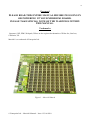
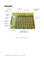
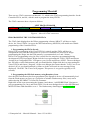
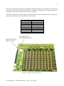
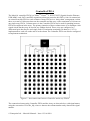
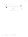
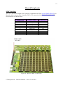
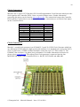
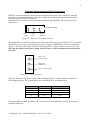
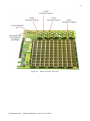
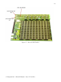
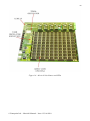
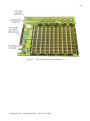
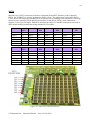
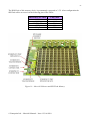
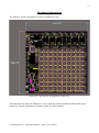
1
MERRICK1 User Manual
Issue – 1.0
© Enterpoint Ltd. – Merrick1 Manual – Issue 1 23.06.2010
2
Kit Contents
You should receive the following items with your Merrick1 Board:
1 - Merrick1 Board
2 - Prog2 (parallel port) or Prog3 (USB) programming cable
© Enterpoint Ltd. – Merrick1 Manual – Issue 1 23.06.2010
3
Contents
Foreword
Trademarks
INTRODUCTION
MERRICK1 BOARD
POWER INPUT
POWER MODULES
POWER REGULATORS
PROGRAMMING MERRICK1
PROGRAMMING THE CONTROLLER FPGA
PROGRAMMING THE ARRAY FPGAS
CONTROLLER FPGA
MAIN FPGA ARRAY
MERRICK PERIPHERALS
MMC INTERFACE
CLOCK GENERATOR 1
CLOCK GENERATOR 2
THERMAL MANGEMENT AND FANS
DIL HEADERS
OSCILLATOR
USER LEDS
USB
SWITCHES
BATTERY BACKUP
SATA
ETHERNET INTERFACE
SPI FLASH
TEMPERATURE SENSORS
MECHANICAL INFORMATION
Medical and Safety Critical Use
Warranty
Support
Backup Support
© Enterpoint Ltd. – Merrick1 Manual – Issue 1 23.06.2010
4
4
5
7
8
8
9
10
10
11
13
15
19
19
20
20
21
23
25
25
27
27
27
29
30
30
32
33
34
34
34
34
4
Foreword
PLEASE READ THIS ENTIRE MANUAL BEFORE PLUGGING IN
OR POWERING UP YOUR MERRICK1 BOARD.
PLEASE TAKE SPECIAL NOTE OF THE WARNINGS WITHIN
THIS MANUAL.
Trademarks
Spartan-6, ISE, EDK, Webpack, Xilinx are the registered trademarks of Xilinx Inc, San Jose,
California, US.
Merrick1 is a trademark of Enterpoint Ltd.
Figure 1 – Merrick1 Board
© Enterpoint Ltd. – Merrick1 Manual – Issue 1 23.06.2010
5
Introduction
Welcome to your Merrick1 board. Merrick1 is Enterpoint’s first High Performance Computing
product aimed at custom high performance processing tasks such as:
Cryptography
Artificial intelligence e.g. Neural Networks and Genetic Algorithms
ASIC prototyping and Emulation
Biometric Modelling and Analysis
Data Mining, Analysis and Extraction.
Financial Modelling and Analysis
Image Processing
Weather System Modelling and Analysis
and many other applications where a high degree of parallel processing is required.
The aim of this manual is to assist in using the main features of Merrick1.
There are features that are beyond the scope of the manual. Should you need to use these features
then please email [email protected] for detailed instructions.
In addition Merrick1 is supported by a wide range of add-on modules. Some examples of these
include:
ADC 7927 MODULE
LED DOT MATRIX MODULE
BUTTONS/SWITCHES/SATA/MEMORY MODULE
RS232 AND RS485 HEADER MODULES
DP83816 ETHERNET MODULE
SD CARD MODULE
DDR2 MODULE
IDE/5V TOLERANT CPLD MODULE
USB MODULE
D/A CONVERTER MODULE
ADV70202 MODULE
We can also offer custom DIL Header modules should you require a function not covered by our
current range of modules. Typical turn around for this service is 6-8 weeks depending upon quantity
ordered and availability of components.
Custom Solutions
The modular nature of the Merrick1 design allows us to derive customer specific variants by
removing part of the array and replacing with custom electronics. It is possible to implement these
changes and build a prototype in a timescale as low as 4 weeks although 8-12 is our typical quote
for a board of this complexity. NRE charges do apply for this service. Contact us on
[email protected] for more details.
© Enterpoint Ltd. – Merrick1 Manual – Issue 1 23.06.2010
6
Merrick1 comes in a single variant based on an XC3SD3400A-4CSG484C Spartan-3A-DSP FPGA.
Should you need more powerful or industrial or automotive grade FPGAs fitted please contact
Enterpoint sales for a quote. Commercial -5 and industrial -4 grade devices are also available;
another alternative offered is to fit XC3SD1800A devices allowing use of free WebpackTM ISETM
software with this board. Contact Enterpoint for details by emailing [email protected] or
telephoning +44 (0) 121 288 3945.
© Enterpoint Ltd. – Merrick1 Manual – Issue 1 23.06.2010
7
Merrick1 Board
Figure 2 – Merrick1 Main Features
© Enterpoint Ltd. – Merrick1 Manual – Issue 1 23.06.2010
8
Power Input
Merrick1 is powered from a nominal 48V power supply via two 6pin connectors which have
contacts rated at 12A maximum. These sockets are manufactured by Phoenix part no. 1757284 and
accept Phoenix plug type 1792799 (available from Farnell and Digikey for example). Merrick1 will
operate over an input voltage range of 36-72V, but the actual voltage chosen must be compatible
with cooling fan power supply requirements.
Power Modules
There are five eighth brick 1.2V power modules on Merrick1. The main array of FPGAs is divided
into 5 sections, each of 2 columns (=20 FPGAs), each of which has a dedicated 1.2V power module
for the FPGA core voltage. These modules are each capable of delivering 30A and are each
protected by a fuse and monitored by an STM6720 Voltage monitor, with the resulting POK signals
being routed to the Controller FPGA. They can be controlled individually from the Controller
FPGA if it is necessary to switch off part of the main array (e.g. to conserve power). When the
Controller FPGA is unconfigured these modules are switched off, so the POWER_ON_N_M signal
for each block must be driven low to switch on each module. There is an LED near each module to
indicate the presence of 1.2V. The connections between the Controller FPGA and the power
modules are shown below.
SIGNAL
POWER_ON_N_M1
POWER_ON_N_M2
POWER_ON_N_M3
POWER_ON_N_M4
POWER_ON_N_M5
POK1
POK2
POK3
POK4
POK5
POWER MODULE
U6_P1
U6_P2
U6_P3
U6_P4
U6_P5
U6_P1
U6_P2
U6_P3
U6_P4
U6_P5
FPGA PIN
Y21
AA20
AB10
AB11
AB21
AB20
AC11
AB12
AB19
AA18
The Merrick board is designed to accept quarter brick modules as an alternative for applications
where a greater Array FPGA core current is required. Currents of up to 100A per section could be
accommodated.
There is one eighth brick 3.3V 30A power module on Merrick1 which supplies power to the
peripherals and the DIL headers, and has an indicator LED and is monitored by the Controller
FPGA on Pin D25. It will not power-up until the 2.5V module is ON.
There is one eighth brick 2.5V 30A module which powers the array FPGA IO, the Ethernet devices,
the Controller FPGA VCCAUX and some Controller IO banks.
There is also a small 6A power module which supplies 1.2V to the Controller FPGA.
© Enterpoint Ltd. – Merrick1 Manual – Issue 1 23.06.2010
9
Figure 3 – Merrick1 Power Supply Modules
Power Regulators
In addition to the 7 power modules these are 6 power regulators on Merrick1. An AP7167 supplies
1V to the MGT IOs of the Controller FPGA, which service the Ethernet connections. ANLT1963
device generates a separate 1.2v supply , also for the Controller MGT interface. Two AP7167
devices each generate 1.8V, one for each Ethernet device. Two LP2995 regulators provide 1.25V
reference voltages for the two Ethernet devices.
WARNING – THE POWER REGULATORS AND MODULES MAY
BECOME HOT IN NORMAL OPERATION ALONG WITH THE
BOARDS THERMAL RELIEF. PLEASE DO NOT TOUCH OR
PLACE HIGHLY FLAMABLE MATERIALS NEAR THESE
DEVICES WHILST THE MERRICK1 BOARD IS IN OPERATION.
© Enterpoint Ltd. – Merrick1 Manual – Issue 1 23.06.2010
10
Programming Merrick1
There are two JTAG connectors on Merrick1: J1, which is the JTAG programming interface for the
Controller FPGA, and J61, which is used to program the Array FPGAs.
The JTAG connectors have a layout as follows:
3V3
GND
TMS
GND
LEFT EDGE OF BOARD
TCK
TDO
TDI
GND
GND
GND
NC
GND
NC
GND
Figure 4 – Merrick1 JTAG connectors
PROGRAMMING THE CONTROLLER FPGA
The JTAG chain displayed on the Xilinx programming software iMPACT will show a single
device, the Virtex5 FPGA. Access to the SPI Flash memory (M25P128) will enable non-volatile
programming of the Controller FPGA.
1. Programming the FPGA directly.
Direct JTAG programming of the Virtex5 FPGA is volatile and the FPGA will lose its
configuration every time the board power is cycled. For sustained use of an FPGA design
programming the design into the Flash memory is recommended (see 2 and 3 below).
Direct JTAG programming using .bit files is useful for fast, temporary programming during
development of FPGA programs. Right click the icon representing the Virtex5 FPGA and choose
‘Assign New Configuration File’. Navigate to your .bit file and choose ‘OPEN’. The next dialogue
box will offer to add a flash memory and you should decline. Right click the icon representing the
Virtex5 FPGA and choose ‘Program’. On the next dialogue box ensure that the ‘Verify’ box is not
checked. (If it is you should uncheck it, failure to do this will result in error messages being
displayed). Click OK. The Virtex5 will program. This process is very quick (typically a few
seconds)
2. Programming the SPI flash memory using Boundary Scan.
Once the SPI Flash memory has been programmed, the Spartan-6 device will automatically load
from the Flash memory at power up. Generation of suitable Flash memory files (.mcs) can be
achieved using ISE iMPACT’s Prom File Formatter.
Right click on the icon representing the Spartan-6 and choose ‘Add SPI/BPI Flash’ Navigate to
your programming file (.mcs) and click OPEN. Use the next dialogue box to select SPI flash and
M25P128. Data width should be set to 1. The flash memory should appear as shown below.
© Enterpoint Ltd. – Merrick1 Manual – Issue 1 23.06.2010
11
Right click on the icon representing the flash memory and choose ‘Program’ to load your program
into the device. It is recommended that options to ‘Verify’ and ‘Erase before programming’ are
chosen. Otherwise all defaults can be accepted. The programming operation will take some time (at
least 3 or 4 minutes).
PROGRAMMING THE ARRAY FPGAS
The second JTAG connector (J61) is used to program the Array FPGAs. The Arrangement of
FPGAs being programmed is controlled by the Controller FPGA configuration and the connections
between J61 and the Controller FPGA are shown below:
J61 PIN
4
6
8
10
SIGNAL
SECONDARY_TMS
SECONDARY_TCK
SECONDARY_TDO
SECONDARY_TDI
FPGA PIN
B16
C17
B17
A17
The Array FPGAs are arranged in five blocks of 20 (2 adjacent columns of FPGAs per block) for
programming and these can be individually turned on and off as required. Partial array operation is
possible e.g. to conserve power and decrease programming time. Simple assignment operations in
the configuration code are used to link the 5 array JTAG chains together. There are 10 TCK and
TMS signals, one for each column of FPGAs, the TCK signals being terminated at the end of the
column: The connections between the array JTAG signals and the Controller FPGA are shown
below.
SIGNAL
LTDI
LTDO
LTCK
LTMS
SECTION5
COLUMNS 1-2
G11
Y16
COL 1 COL 2
AA9
AB9
AD14
AD13
SECTION4
COLUMNS 3-4
H19
AA14
COL 3 COL 4
AC9
AD9
AE13
AF13
SECTION3
COLUMNS 5-6
H18
AA13
COL 5 COL 6
AD8
AC8
AF14
AF15
SECTION2
COLUMNS 7-8
G16
Y7
COL 7 COL 8
AC7
AD6
AE15
AD15
SECTION1
COLUMNS 9-10
G15
AA17
COL 9 COL10
AF3
AF4
AD16
AE16
For example if the secondary JTAG chain was required to only address columns 1 and 2 of the
Array FPGAs, the Controller FPGA would make the following assignments:
LTMS1 <= SECONDARY_TMS
LTMS2 <= SECONDARY_TMS
LTCK1 <= SECONDARY_TCK
LTCK2 <= SECONDARY_TCK
LTDI1 <= SECONDARY_TDI
SECONDARY_TDO <= LDTO1
For all columns to be programmed the following assignments would be made:
ALL 10 LTMS SIGNALS <= SECONDARY_TMS
ALL 10 LTCK SIGNALS <= SECONDARY_TCK
LTDI1 <= SECONDARY_TDI
LTDI2 <= LTDO1
LTDI3 <= LTDO2
LTDI4 <= LTDO3
LTDI5 <= LTDO4
SECONDARY_TDO <= LDTO5
© Enterpoint Ltd. – Merrick1 Manual – Issue 1 23.06.2010
12
Once the Controller FPGA has been configured to link the required Array FPGA JTAG connections
to J61 the Array JTAG chain should be visible on an iMPACT boundary scan. Programming of the
Array FPGAs is achieved using a .bit file and so is volatile.
The PROG_B signals for each column of Array FPGAs are connected together and the resulting 10
signals are routed to the Controller FPGA as shown below:
ARRAY COLUMN
1
2
3
4
5
6
7
8
9
10
FPGA PIN – PROG B
AE10
AD10
W8
W9
AD11
AE11
V9
V8
AE12
AF12
Figure5 – Merrick1 JTAG connectors
© Enterpoint Ltd. – Merrick1 Manual – Issue 1 23.06.2010
13
Controller FPGA
The Merrick1 controller FPGA is a XilinxTM VirtexTM-5 XC5VLX30T. Signals from the Ethernet,
USB, MMC card, SATA and DIL expansion sockets are routed to this FPGA, Also 14 connections
are routed from this FPGA to each column of Array FPGAs in a ‘daisy chain’ arrangement, so that
there are a total of 140 routes between the controller and the array, with a maximum of 14 routes to
any single array FPGA. Column routes via the Controller FPGA can be used for patching between
FPGAs not adjacent in the array. The primary intention of these column routes is to distribute clock
signals clocks but they may be used in any fashion desired. These wires are configured as 7
differential pairs but may be used single ended. Termination (nominally 50 ohms) to 1.25V is
implemented on each wire at the end of each column. The Controller FPGA can also be configured
to implement termination.
Figure6 – Interconnections between Controller and Array FPGAs
The connections between the Controller FPGA and the Array are shown below, with signal names
using the convention CLOCKx_My, where x denotes the column number and y denotes the signal
number
© Enterpoint Ltd. – Merrick1 Manual – Issue 1 23.06.2010
14
SIGNAL
SIGNAL
NAME
1
2
3
4
5
6
7
8
9
10
11
12
13
14
CLOCKx_M0
CLOCKx_M1
CLOCKx_M2
CLOCKx_M3
CLOCKx_M4
CLOCKx_M5
CLOCKx_M6
CLOCKx_M7
CLOCKx_M8
CLOCKx_M9
CLOCKx_M10
CLOCKx_M11
CLOCKx_M12
CLOCKx_M13
CONTROLLER FPGA CONNECTIONS
Col.1
H21
G20
G24
F24
G25
H26
E25
E26
F22
F23
H22
G22
E22
E23
Col.2
K21
J21
J26
J25
K25
L24
J23
H23
L22
L23
K23
K22
J24
H24
Col.3
M24
M25
L25
K26
T23
T24
H9
G10
P23
P24
R22
R23
M22
N22
Col.4
G26
F25
N23
N24
R25
P25
T25
U25
F20
G21
M26
N26
E21
E20
Col.5
V24
U24
U22
T22
AD21
AC21
V23
W24
W21
V21
AA23
AB24
R21
P21
Col.6
Y25
Y26
W25
W26
AE20
AF20
AE23
AF23
AD23
AE22
AD20
AD19
W23
Y23
Col.7
AA24
AB25
V26
U26
AF19
AF18
V22
U21
R26
P26
AD18
AE18
AB26
AA25
Col.8
AD24
AD25
AE26
AE25
E16
D16
E15
D15
N21
M21
D18
E17
AD26
AC26
Col.9
AB22
AC22
AC23
AC24
G14
H13
G12
F13
E11
F12
D13
D14
AF24
AF25
Col.10
AF17
AE17
Y22
A22
F17
G17
F19
E18
F14
F15
AF9
AF10
AE21
AF22
The Controller FPGA also connects to the two Ethernet Controllers, the SATA connectors, the two
clock generators, two oscillators, the USB interface, 8 LEDs, 2 temperature sensors, an 8-way
switch, the system fans and a Data Card holder. It also controls the Main Array JTAG chains and
controls and monitors the Main Array power modules.
Figure7 – Merrick1 FPGAs
© Enterpoint Ltd. – Merrick1 Manual – Issue 1 23.06.2010
15
Main FPGA Array
Figure8 – Interconnections on main array
The main feature of Merrick1 is a 10 x 10 array of XilinxTM SpartanTM-3A DSP XC3SD3400A4CSG484C FPGAs. Each array FPGA has 40 wired connections on each side to its 4 adjacent
FPGAs or I/O connectors. These are wired as differential pairs but may be used single ended. The
I/O voltage is fixed at 2.5V. Using a standard configuration of 20 wires in each direction, LVDS as
I/O standard, it is possible to implement a connection scheme of 1 forward clock + 1 alignment
strobe + 8 data lines giving 500+ Mbyte/s between adjacent FPGAs in each direction.
1600 user I/O are available around the edges of the main FPGA array on the 40 50-way connectors.
20 are on the upper surface of the board and 20 on the underside. The connectors used are Vertical
boxed 2x25 1.27mm IDC connectors (compatible with TDI type 222804-00225). 3.3V and 0V are
also available on these connectors. Each connector is dedicated to a single FPGA and supports 20
pairs of LVDS or 40 single ended signals for High speed signalling.
© Enterpoint Ltd. – Merrick1 Manual – Issue 1 23.06.2010
16
Each individual FPGA has 174 connections in total. There are 40 signals on each side of each
FPGA which connect to the neighbouring FPGAs so that the LEFT1 connection of one FPGA
connects to the RIGHT1 connection of its left hand side neighbour. Similarly the TOP1 connection
of one FPGA connects to the BOTTOM1 connection of the FPGA immediately above it in the
array. There are also 14 connections which are daisy-chained along each column of 10 FPGAs and
connect to the Controller FPGA, which are referred to as CLOCK signals The pinout of each Array
FPGA is shown below:
SIGNAL
NUMBER
0
1
2
3
4
5
6
7
8
9
10
11
12
13
14
15
16
17
18
19
20
21
22
23
24
25
26
27
28
29
30
31
32
33
34
35
36
37
38
39
40
RIGHT
LEFT
BOTTOM
TOP
G3
F3
C1
C2
F5
F4
H4
H3
H1
G1
R5
P4
E4
E3
N1
M1
P2
P1
R1
R2
J1
H2
U5
U4
L1
K1
U1
T1
T4
R3
W2
W3
M2
L3
V3
V4
W1
Y1
V1
U2
F19
F18
D21
D22
F21
E20
H22
G22
J19
H20
N21
M20
D20
E19
N22
M22
N20
N19
R22
P22
K20
J20
U22
T22
L22
K22
U20
T20
R19
R20
W22
Y22
K19
K18
W19
V20
Y21
AA22
U18
U19
B3
A3
D5
C4
B4
A4
F8
E8
C7
D7
B6
A7
A6
A5
G8
F9
D9
C8
B11
A11
C9
D10
E13
D13
C13
C12
B20
A19
B15
A14
A17
A16
D19
C19
C15
D14
C17
B17
C18
B19
Y4
W5
AA4
AB4
AB6
AB5
V8
W8
AA8
AB7
U9
V10
U8
V7
AA10
AB10
Y9
Y8
U10
V11
Y10
T11
AB14
AA15
W14
Y13
AB20
AA20
U15
U14
Y19
Y18
AA19
AB19
V16
U16
Y16
Y17
AB17
AB18
CLOCK
AA14
AB13
V12
U12
R18
P19
B9
A9
D6
C6
F16
E16
K3
K2
The FPGAs at the edges of the array connect to 50-way 1.27mm IDC connectors along one side
instead of interfacing to the neighbouring FPGA. The connections between the FPGAs and
connectors are shown below:
© Enterpoint Ltd. – Merrick1 Manual – Issue 1 23.06.2010
17
CONNECTOR PIN
1
2
3
4
5
6
7
8
9
10
11
12
13
14
15
16
17
18
19
20
21
22
23
24
25
26
27
28
29
30
31
32
33
34
35
36
37
38
39
40
41
42
43
44
45
46
47
48
49
50
TOP
CONNECTOR
GND
GND
Y4
W5
AA4
AB4
AB6
AB5
U8
V7
U9
V10
3.3V
3.3V
V8
W8
AA8
AB7
AA10
AB10
Y9
Y8
Y10
T11
GND
GND
U10
V11
W14
Y13
AB14
AA15
U15
U14
V16
U16
3.3V
3.3V
Y16
Y17
Y19
Y18
AB17
AB18
AA19
AB19
AB20
AA20
GND
GND
FPGA PIN
BOTTOM
LEFT
CONNECTOR CONNECTOR
GND
GND
GND
GND
B3
F19
A3
F18
D5
D21
C4
D22
B4
F21
A4
E20
A6
D20
A5
E19
B6
J19
A7
H20
3.3V
3.3V
3.3V
3.3V
F8
H22
E8
G22
C7
K20
D7
J20
G8
L22
F9
K22
D9
K19
C8
K18
C9
N21
D10
M20
GND
GND
GND
GND
B11
N22
A11
M22
C13
N20
C12
N19
E13
R22
D13
P22
B15
R19
A14
R20
C15
U22
D14
T22
3.3V
3.3V
3.3V
3.3V
C17
U20
B17
T20
A17
U18
A16
U19
C18
W19
B19
V20
D19
W22
C19
Y22
B20
Y21
A19
AA22
GND
GND
GND
GND
© Enterpoint Ltd. – Merrick1 Manual – Issue 1 23.06.2010
RIGHT
CONNECTOR
GND
GND
C1
C2
E4
E3
F5
F4
G3
F3
H1
G1
3.3V
3.3V
H4
H3
J1
H2
L1
K1
M2
L3
N1
M1
GND
GND
R5
P4
P2
P1
R1
R2
T4
R3
U1
T1
3.3V
3.3V
U5
U4
V1
U2
V3
V4
W1
Y1
W2
W3
GND
GND
18
The connector pins are defined as follows, viewed from above:
P2
P50
P1
P49
Polarising Key
Figure9 – Merrick1 Connector pinout
© Enterpoint Ltd. – Merrick1 Manual – Issue 1 23.06.2010
19
Merrick Peripherals
MMC Interface
There is an SD Secure Digital Card Connector (compatible with Toby type 412D02F-09PC003) on
Merrick which connects to the Controller FPGA. The connections between the Controller and the
card connector are shown below:
CARD READER
CONNECTION
WP1
WP2
CD1
CD2
1
2
5
7
8
9
POWER CONTROL
SIGNAL NAME
FPGA PIN
MMC_WP1
MMC_WP2
MMC_CD1
MMC_CD2
MMC_CD/DAT_3
MMC_CMD
MMC_CLK
MMC_DAT0
MMC_DAT1
MMC_DAT2
MMC_VD3V3_ON_N
B22
D21
A22
A23
B21
C19
C21
A24
D19
B20
C22
Figure10 - Merrick1 MMC Card Holder
© Enterpoint Ltd. – Merrick1 Manual – Issue 1 23.06.2010
20
Clock Generator 1
Merrick1 has a Cypress CY22394 three-PLL Serial-Programmable Clock Generator which provides
clock signals to the Controller FPGA. It has a crystal oscillator source. Further information
concerning this device can be found at www.cypress.com The connections between the Controller
FPGA and the CY22394 device are shown below. All these connections are to Global Clock inputs
on the Controller FPGA.
CY22394 PIN
10
9
1
6
16
15
7
8
13
12
SIGNAL NAME
CLK_A
CLK_B
CLK_C
CLK_X
CLK_SHUTDOWN_N
CLK_SUSPEND_N
CLK-P
CLK+P
CLK_SCLK
CLK_SDAT
FPGA PIN
AB15
AC16
AB16
AC17
AC12
AC13
AB17
AC18
AC14
AB14
Clock Generator 2
Merrick1’s second clock generator is an ICS844071 Crystal-To-LVDS Clock Generator which has
one differential LVDS output for high speed serial interfaces. It is intended to be used as the SATA
clock, in which case a 25MHz oscillator should be used in the 8 pin 3.3V DIL socket J72. The
ICS844071 has excellent <1ps phase jitter performance. For further information on this device
please refer to www.idt.com. The output of this Clock generator is connected into the four
MGTREFCLK inputs of the Controller FPGA i.e. K4,K3,T4,T3,D4,D3 and AB4,AB3.
Figure11 – Merrick1 Clock Generators
© Enterpoint Ltd. – Merrick1 Manual – Issue 1 23.06.2010
21
Thermal Management and Fan Connectors
Merrick1 can run simple tasks with passive cooling but will require active cooling by fans and
heatsinks to maximise performance. We have a range of cooling support options for this board.
Please contact us for more information.
Merrick1 has four 3 pin fan connectors with rpm monitoring capability. The pinout of the fan
connectors is:
TOP EDGE OF BOARD
PIN1
-VE/0v
PIN2
+VE
PIN3
SPEED
Figure 12 - Merrick1 fan connector pinout
By default the fan connectors connect between the main 48V supply, but a header (J73) is provided
so that the user can connect an alternative fan power supply, which must be reference to the main
input 0V. The user’s fan supply should be connected with +ve on pin 3 and 0V on pin2 of J73. If
48V fans are fitted it is necessary to link from J73 Pin 1 to Pin3 otherwise the fans will not be
powered.
PIN1 +VE
SUPPLY 48V
PIN2 FAN
SUPPLY 0V
PIN3 +VE TO FANS
Figure 13 - J73 connections
The four ‘fan speed’ signals are routed to the Controller FPGA via optocouplers to protect the
FPGA input circuitry. The connections to the Controller FPGA are shown below:
FAN
1
2
3
4
CONNECTOR
J3
J4
J5
J6
FPGA PIN
A20
A25
D20
A18
The optocouplers each have a jumper (J7, J8, J9 and J50) which should be fitted if the fan speed
signal is being used.
© Enterpoint Ltd. – Merrick1 Manual – Issue 1 23.06.2010
22
Figure 14 – Merrick1 Fan Connectors
© Enterpoint Ltd. – Merrick1 Manual – Issue 1 23.06.2010
23
DIL Headers
The DIL Headers provide a simple mechanical and electrical interface for add-on modules. The
connectors on this header are on a 0.1inch, 2.54mm, pitch and allow either custom modules or strip
board to be fitted. The headers have a row of permanent positive power sockets (3.3V) above J58
and a row of permanent GND (0V) sockets below J57.
There are 20 IOs routed from the Controller FPGA to the DIL headers. The remaining pins are used
for mechanical support and for power supply (3.3V and 0V) to the modules or user add-on board.
Voltages outside the range 0V to 3.3V must not be applied to the DIL headers. The Virtex5 has an
absolute maximum IO input voltage of 4V.
The connections between the DIL the headers and the Controller FPGA are shown below:
LEFT EDGE OF BOARD
J58
C11
D11
B12
C12
R8
R7
N8
P8
T7
E22
J57
3.3V
3.3V
3.3V
3.3V
3.3V
3.3V
3.3V
3.3V
3.3V
3.3V
3.3V
3.3V
3.3V
3.3V
3.3V
3.3V
3.3V
3.3V
3.3V
3.3V
3.3V
3.3V
3.3V
3.3V
3.3V
3.3V
3.3V
3.3V
3.3V
3.3V
3.3V
3.3V
3.3V
3.3V
0V
0V
0V
0V
0V
0V
0V
0V
0V
0V
0V
0V
0V
0V
0V
0V
0V
0V
0V
0V
0V
0V
0V
0V
0V
0V
0V
0V
0V
0V
0V
0V
0V
0V
© Enterpoint Ltd. – Merrick1 Manual – Issue 1 23.06.2010
B4
B5
D5
E5
M6
N7
P6
N6
A12
H19
24
Figure 15 – Merrick1 DIL Headers
© Enterpoint Ltd. – Merrick1 Manual – Issue 1 23.06.2010
25
Oscillator
There are 2 oscillator sockets on Merrick1 for users to select their own oscillator frequency. These
support 3.3V, 8-pin DIL outline, oscillator crystals. One of these is dedicated to the SATA clock
generator. There is also a fixed 25MHz oscillator and a 0-400MHz clock generator which has a
crystal oscillator source.
The fixed 25MHz signal is routed directly to the Controller FPGA pin AC19, which is a Global
Clock input.
The Virtex5 LX30T has two Clock Management tiles, each of which contains two Digital Clock
Multipliers and one Phase Locked Loop. to produce multiples, divisions and phases of clock
signals. Please consult the Virtex5 datasheet available from the Xilinx website at
http://www.xilinx.com if multiple clock signals are required.
User LEDs
On Merrick1 there are 8 LEDS which connect to the Controller FPGA and one on each of the 100
Array FPGAs. These are all user-controllable LEDs and are connected to the FPGAs as indicated
below:
HOST DEVICE
Controller FPGA
Array FPGAs
DESIGNATOR
LED2
LED3
LED4
LED5
LED6
LED7
LED8
LED9
LED1
FPGA PIN
C13
C14
B14
A13
A14
A15
B15
C16
E7
Additionally there are 5 LEDs connected to each Ethernet Controller device. These are not available
for user control. There are also 7 LEDs indicating the presence of power from 7 of the 8 power
modules.
© Enterpoint Ltd. – Merrick1 Manual – Issue 1 23.06.2010
26
Figure 16 – Merrick1 Oscillators and LEDs
© Enterpoint Ltd. – Merrick1 Manual – Issue 1 23.06.2010
27
USB
The USB interface on the Merrick1 is achieved using an FT232R USB to serial
UART interface and a Mini-B type connector. The datasheet and drivers for this
device are available from http://www.ftdichip.com. When appropriate drivers are
installed the Merrick1 USB port should be detected as a serial port. Alternative data
optimised drivers are also available from FTDI.
The FT232R is connected to the Controller FPGA and provided a simple UART, or
other converter, is implemented then the data sent over the USB serial port can be
used either as control and/or data information. This allows a host computer to act in a
number of ways including system control and data storage functions. The
connections between the USB device and the FPGA are shown below:
FT232R
CTS#
DCD#
DSR#
RI#
RTS#
DTR#
TXD
RXD
FPGA PIN
C24
B26
D23
D24
C23
B25
B24
C26
Switches
Merrick1 has a bank of 8 2-position DIP switches. To use these switches it is necessary to set the IO
pins connected to the switches to have a pull up resistor setting in the constraints file. The switches
are connected to the following IO pins. Switch 1 is furthest from the Virtex5 device.
SWITCH
1
2
3
4
5
6
7
8
FPGA PIN
AA5
AB5
AB6
AB7
AE6
AF5
AE5
AD4
Battery Backup
The Merrick1 has a battery holder which is available to provide battery backup to the FPGA. It is
connected to the Controller FPGA on Pin J19. The battery holder accepts a 3V Lithium battery size
CR1220 or equivalent. Battery backup allows the use of an encrypted bitstream for the Controller
FPGA and facilitates IP locking to an individual board etc.
© Enterpoint Ltd. – Merrick1 Manual – Issue 1 23.06.2010
28
Figure 17 – Merrick1 USB, Switches and Battery
© Enterpoint Ltd. – Merrick1 Manual – Issue 1 23.06.2010
29
SATA
Merrick1 has 8 SATA connectors which are connected to the MGT interface of the Controller
FPGA. An ICS844071 is used to generate the SATA Clock. The connections between the SATA
Clock, the SATA connectors and the FPGA are shown below (omitting series capacitors, J56 being
nearest to the Controller FPGA and J69 the furthest). Each pair of SATA Clock connections
supplies 2 sets of SATA inputs. Half the 8 channels have their TX and RX connections reversed to
allow board stacking connections using standard SATA cables.
J56 PIN
PIN 2
PIN 3
PIN 5
PIN 6
CLOCK+
CLOCKJ64 PIN
PIN 2
PIN 3
PIN 5
PIN 6
CLOCK+
CLOCK-
FPGA J67 PIN
PIN
B2
PIN 2
C2
PIN 3
C1
PIN 5
D1
PIN 6
D4
CLOCK+
D3
CLOCK-
FPGA J62 PIN
PIN
G2
PIN 2
F2
PIN 3
F1
PIN 5
E1
PIN 6
D4
CLOCK+
D3
CLOCK-
FPGA
PIN
H2
J2
J1
K1
K4
K3
FPGA J65 PIN
PIN
P2
PIN 2
R2
PIN 3
R1
PIN 5
T1
PIN 6
T4
CLOCK+
T3
CLOCK-
FPGA J68 PIN
PIN
W2
PIN 2
V2
PIN 3
V1
PIN 5
U1
PIN 6
T4
CLOCK+
T3
CLOCK-
FPGA
PIN
Y2
AA2
AA1
AB1
AB4
AB3
Figure 18 – Merrick1 SATA Connectors
© Enterpoint Ltd. – Merrick1 Manual – Issue 1 23.06.2010
J63 PIN
PIN 2
PIN 3
PIN 5
PIN 6
CLOCK+
CLOCKJ69 PIN
PIN 2
PIN 3
PIN 5
PIN 6
CLOCK+
CLOCK-
FPGA
PIN
N2
M2
M1
L1
K4
K3
FPGA
PIN
AD2
AE2
AD1
AC1
AB4
AB3
30
Ethernet Interface
Merrick1 has two 10/100/1000 base-T connections which interface to the MAC hard IP cores within
the Controller FPGA. The Ethernet signals each pass through a transformer to a DP8365DVH
Ethernet Phy device. The signals are then passed to the Controller FPGA as shown below:
SIGNAL
ETHERNET1
ETHERNET2
ETH_RX0
A9
W5
ETH_RX1
A8
W6
ETH_RX2
ETH_RX3
E8
E7
G4
H4
ETH_RX4
ETH_RX5
B9
C8
V6
V7
ETH_RX6
E6
J5
ETH_RX7
ETH_TX0
D6
H7
J6
Y6
ETH_TX1
ETH_TX2
G7
F7
Y5
G6
ETH_TX3
ETH_TX4
F8
F9
H6
Y4
ETH_TX5
G9
W4
ETH_TX6
ETH_TX7
H8
J8
G5
F5
ETH_CK_MAC_FREQ
ETH_TX_ER
B11
C9
R6
U7
ETH_TXEN_ER
D8
T8
ETH_SEL1
ETH_SEL0
C7
C6
K5
L5
ETH_TCK
ETH_MDIO
A7
B7
K6
K7
ETH_MDC
CLOCK_ETH_25MHZ
D10
B6
U6
U5
ETH_RESET_N
B6
K8
ETH_CLK_TO_MAC
ETH2_INT_N
A5
B10
L7
T5
ETH2_RXDV_ER
ETH2_RCK
A10
A4
R5
M7
ETH2_RX_CLK
A3
L8
SPI Flash Memory
The M25P128 SPI flash memory device configures the Controller FPGA when it is powered
providing a suitable bitstream is programmed into the device. The M25P128 has a capacity of
128Mbits with a single configuration bitstream for Merrick1 Controller FPGA taking 3.2MB. Any
remaining space can be used for alternative configurations or code and data storage e.g.
MicroblazeTM code.
© Enterpoint Ltd. – Merrick1 Manual – Issue 1 23.06.2010
31
The HOLD pin of this memory device is permanently connected to 3.3V. After configuration the
SPI Flash can be accessed via the following pins of the FPGA:
M25P128 FUNCTION
CCLK
MOSI
WRITE_SPI
DIN
CSO_B
FPGA PIN
J11
AA12
D26
J10
Y12
Figure 19 – Merrick1 Ethernet and SPI Flash Memory
© Enterpoint Ltd. – Merrick1 Manual – Issue 1 23.06.2010
32
Temperature Sensors
There are two temperature sensors (type LM75C) on Merrick1 which have a 2-wire serial interface
and outputs which behave as over-temperature warnings. The connections to the Controller FPGA
are shown below:
SIGNAL
SDA
SCL
OVER-TEMPERATURE
FPGA PIN
(SENSOR1)
W11
Y10
Y20
The temperature sensors are located on the underside of the board:
© Enterpoint Ltd. – Merrick1 Manual – Issue 1 23.06.2010
FPGA PIN
(SENSOR2)
AA19
Y11
AA18
33
Mechanical Information
The Merrick1 board is designed to fit into a standard 9U rack.
Figure 20 – Mechanical Arrangement of Merrick1
All dimensions are shown in millimetres. If you need any further mechanical information please
contact us. Contact information is shown on page 34 of this manual.
© Enterpoint Ltd. – Merrick1 Manual – Issue 1 23.06.2010
34
Medical and Safety Critical Use
Merrick1 boards are not authorised for the use in, or use in the design of, medical or other safety
critical systems without the express written person of the Board of Enterpoint. If such use is
allowed the said use will be entirely the responsibility of the user. Enterpoint Ltd will accepts no
liability for any failure or defect of the Merrick1 board, or its design, when it is used in any medical
or safety critical application.
Warranty
Merrick1 comes with a 90 day return to base warranty. Do not attempt to solder connections to the
Merrick1. Enterpoint reserves the right not honour a warranty if the failure is due to soldering or
other maltreatment of the Merrick1 board.
Outside warranty Enterpoint offers a fixed price repair or replacement service. We reserve the
right not to offer this service where a Merrick1 has been maltreated or otherwise deliberately
damaged. Please contact support if need to use this service.
Other specialised warranty programs can be offered to users of multiple Enterpoint products.
Please contact sales on [email protected] if you are interested in these types of warranty,
Support
Enterpoint offers support during normal United Kingdom working hours 9.00am to 5.00pm. Please
examine our Merrick1 FAQ web page and the contents of this manual before raising a support
query. We can be contacted as follows:
Telephone
Email
- ++44 (0) 121 288 3945
- [email protected]
Backup Support
We can offer a guaranteed product replacement plan to purchasers of Merrick1. For a fixed monthly
fee you get a time guaranteed replacement board if your board should fail in service. Please contact
us for more details of this service
© Enterpoint Ltd. – Merrick1 Manual – Issue 1 23.06.2010