1
ISRN UTH-INGUTB-EX-E-2013/04-SE
Examensarbete 15 hp
Juni 2013
Completion of the software required
for a high-temperature DLTS setup
Rasmus Jansson
Abstract
Completion of the software required for a
high-temperature DLTS setup
Rasmus Jansson
Teknisk- naturvetenskaplig fakultet
UTH-enheten
Besöksadress:
Ångströmlaboratoriet
Lägerhyddsvägen 1
Hus 4, Plan 0
Postadress:
Box 536
751 21 Uppsala
The main purpose of this thesis was to examine the communication problems with
the DLTS set up in the Division for Electricity at Ångström Laboratory in Uppsala,
Sweden, and to make the DLTS software complete. The set up consisted of a C/V
meter, a pulse generator, a temperature controller and a PC with a control program
written in LabVIEW. It was found that the software had been constructed to fit
another set of instruments than the set up currently used at Ångström Laboratory.
The task was therefore to properly integrate the correct control commands of those
instruments into the software.
Telefon:
018 – 471 30 03
Telefax:
018 – 471 30 00
Hemsida:
http://www.teknat.uu.se/student
Handledare: Markus Gabrysch
Ämnesgranskare: Saman Majdi
Examinator: Nora Masszi
ISRN UTH-INGUTB-EX-E-2013/04-SE
Tryckt av: Uppsala Universitet, Uppsala
Sammanfattning
(a summary in Swedish)
Halvledare används inom flera områden i elektrotekniska sammanhang. Detta för att deras elektriska egenskaper med lätthet kan formas och styras genom en process som
kallas dopning. Ett vanligt material med halvledande egenskaper som används för att
tillverka olika elektroniska komponenter är kisel och olika föreningar med kisel. Vid
sammansättningen (dopningen) av dessa kiselföreningar bildas också defekter i materialet. Dessa defekter kan beskrivas som kemiska orenheter som markant påverkar den
elektriska strömmen genom materialet. Defekterna har den egenheten att de fångar upp
laddningsbärare, tex elektroner, och för att fria dem krävs en viss mängd energi, i denna
rapport används värmeenergi. En metod för att detektera djupa defekter (på engelska
deep-level defects) i en halvledare är deep-level transient spectroscopy, eller kort DLTS.
Metoden går ut på att först tömma defekterna, i provet, på de laddningsbärare som erhållit tillräckligt med energi och sedan låta dessa falla tillbaka till defekterna för att
sedan utföra en tömning igen. Processen för att fylla defekterna sker relativt snabbt medan för att tömma dem på laddningsbärare sker över en viss tid. Över denna tid kommer
kapacitansen i provet att ändras som funktion av tid och det är denna kapacitansändring
som genom signalbehandling ger upphov till en DLTS signal.
Detta projekts huvudsyfte var att undersöka problemen med, samt färdigställa, kommunikationen mellan mätinstrumenten och kontrollprogrammet som utgjorde
uppställningen för DLTS mätningar på Ångströms Laboratorium i Uppsala. Uppställningen bestod utav en kapacitansmätare, en pulsgenerator, en temperaturkontroll samt
en PC med integrerat kontrollprogram utvecklat i programmeringsmiljön LabVIEW.
Problemet bestod i att kontrollprogrammet ej hade blivit uppdaterat enligt det instrument som användes på Ångström. Programmet var konstruerat utav en forskningsgrupp
i Norge som använde mätinstrument av andra märken och därför skiljde sig de kontrollkommandon som skulle skickas från programmet. Uppgiften bestod alltså av att
integrera de korrekta kommandona för uppställningen på Ångström samt se till att kommunikationen fungerade.
Key words: Semiconductors, DLTS, LabVIEW, VISA, GPIB, 488.2
I
Preface
This thesis had not been finished without Markus Gabrysch's supervision and guidance,
nor without Florian Burmeister's support and encouragement during my time with the
group.
I also would like to thank my topic examiner Saman Majdi for his determination to always help in all ways possible.
Supervisor: Markus Gabrysch
Topic examiner: Saman Majdi
Examiner: Nora Masszi
Author: Rasmus Jansson
Ångström Laboratory, Uppsala, Sweden, 2013-06
II
Contents
Abbreviations................................................................................1
1 Introduction..............................................................................2
1.1 Background..........................................................................................................2
1.2 Assignment............................................................................................................3
2 Theory.......................................................................................4
2.1 Atomic- & Band structure in solid-state physics...............................................4
2.1.1 Valence band & conduction band...................................................................5
2.2 Defects...................................................................................................................5
2.2.1 Deep-level defects..........................................................................................6
2.2.2 Traps...............................................................................................................6
2.3 Deep-Level Transient Spectroscopy...................................................................6
2.3.1 The capacitance transient...............................................................................7
2.3.2 Window & weighting functions.....................................................................8
2.3.3 DLTS signal....................................................................................................9
2.4 Analysis of DLTS & Arrhenius plot..................................................................11
2.5 LabVIEW............................................................................................................11
2.5.1 VISA/GPIB..................................................................................................13
3 Method....................................................................................16
3.1 Experimental setup............................................................................................16
3.2 Implementation..................................................................................................17
3.2.1 Controls........................................................................................................18
3.2.2 Indicators......................................................................................................21
4 Results.....................................................................................23
5 Discussion & Analysis............................................................24
5.1 Communications................................................................................................24
5.2 Yudian control AI-518........................................................................................24
5.3 DLTS main VI....................................................................................................25
6 Summary & conclusions........................................................26
6.1 Outlook................................................................................................................26
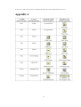
Appendix A.................................................................................27
References...................................................................................28
III
List of figures
Figure 2.1: Silicon crystal..................................................................................................4
Figure 2.2: Bonds in Silicon crystal at T=0K and T>0K...................................................4
Figure 2.3: Band structure for metals, semiconductors & insulators................................5
Figure 2.4: The construction of a DLTS signal from the capacitance transients...............7
Figure 2.5: The transient starts after the falling edge of the voltage pulse........................8
Figure 2.6: Capacitance transient with eight measurement points weighted with three
windows of the lock-in function, where Cj is the capacitance value of the
j'th point. The windows' value for this particular transient are represented by
the symbols to the right of the windows.......................................................10
Figure 2.7: A typical DLTS signal with three windows, where the values for each window from the transient in Figure 2.6 are also shown....................................11
Figure 2.8: Block diagram of a simple VI program.........................................................12
Figure 2.9: Front panel of a simple VI program..............................................................12
Figure 2.10: LabVIEW functions palette.........................................................................13
Figure 2.11: Block diagram of a test using GPIB protocol with an external device.......14
Figure 2.12: Block diagram of a test using VISA protocol with an external device.......15
Figure 3.1: LabVIEW VI hierarchy of the DLTS software.............................................17
Figure 3.2: DLTS software, overview of the front panel in LabVIEW...........................18
Figure 3.3: Controls of the DLTS software.....................................................................19
Figure 3.4: The pulse's parameters (Vbias, Vpulse and pulse width), for point 2, 3 and 6.
In this thesis Vpulse was chosen to be 5V and Vbias is -5V........................20
Figure 3.5: For point 7 & 8, Lock-in function with three windows displaying the minimum window length and relation between the window's lengths. The next
following window is always twice as large as the current window..............20
Figure 3.6: Two transients, one with the raw data from the CV meter and the other with
the signal processed data..............................................................................21
Figure 3.7: Temperature indicators of the front panel and the STOP button...................21
Figure 3.8: The measured capacitance during the bias voltage as a function of temperature.................................................................................................................22
Figure 4.1: CV-measurement, capacitance in mF on y-axis and voltage in V on x-axis.23
Figure 4.2: DLTS signal using 6 different lock-in windows (Temperature on the x-axis
and DLTS signal on y-axis)..........................................................................23
List of tables
Table 3.1: Instrument setup..............................................................................................16
Table A.1: NI 488.2/VISA equivalents............................................................................27
IV
Bachelor thesis: COMPLETION OF THE SOFTWARE REQUIRED FOR A HIGH-TEMPERATURE DLTS SETUP
Abbreviations
Cj
The capacitance of the j'th measurement point, [F]
DLTS
Deep-level transient spectroscopy
DUT
Device Under Test
EC
Energy level of the bottom of the conduction band (referred to as the
conduction band in the text), [eV]
Eg
Forbidden energy range between the EC and EV, called bandgap, [eV]
EV
Energy level of the top of the valence band (referred to as the valence band
in the text), [eV]
GPIB
General Purpose Interface Bus
HP
Hewlett Packard
Ni
The number of measurements / measurement points for the i'th window. It
is decided by N i=2i
Si
DLTS signal for the i'th window
T
Temperature, [K]
VISA
Virtual Instrument Software Architecture
wi
The i'th window/weighting function
1
Bachelor thesis: COMPLETION OF THE SOFTWARE REQUIRED FOR A HIGH-TEMPERATURE DLTS SETUP
1 Introduction
Semiconductors are widely used in electronic devices. Their electrical properties are
easily controlled and thus they may fit in many different applications. But no electrical
device is flawless. For example, when a semiconductor is doped, in order to get some
desired property, the semiconductor also obtains some chemical impurities called deeplevel defects. The deep-level defects affect the forward and reverse current significantly
and increases the noise in transistors. Identification of defects and characterisation of
their impact on semiconductors properties is a very important issue since they so radically can change the electrical transport properties of a semiconductor due to thermal
heating for example [1].
There is a constant struggle going on to build electronic devices that operate with as
small losses as possible. The most fundamental and first step in the construction of an
electronic device is the choice of material. One of the most common semiconducting
material is silicon and different compounds of silicon, but for more extreme cases, for
example where electronic devices are exposed to very high temperatures, a harder material, that can withstand the extreme environment, is needed. Therefore, the interest of
using diamond for more extreme electronic applications has increased in the past few
years.
Synthetic diamond has been developed for decades, but was not pure enough to be considered for electrical applications. This, however, is not the case today where a new
method has made it possible to grow diamond with a small concentration of defects. Because of this, the interest of using diamond for electrical applications has become
greater, but, as well as in any other semiconducting materials, there are always some defects present that need to be characterized [2]. In the Division for Electricity at
Ångström Laboratory there is an ongoing project focusing on characterizing deep-level
defects in synthetic diamond that are situated deep in the bandgap. Such deep levels
have a long lifetime and might have a big impact on the electrical properties of diamond
devices. The method that is being used is called deep-level transient spectroscopy
(DLTS). It is a sensitive quantitative characterization method for deep-level defects.
1.1 Background
In the Division of Electricity the DLTS setup consisted of a C-meter, a pulse generator
and a temperature controller. These instruments were controlled with a computer program, which had originally been developed by a Ph.D student at KTH and revised by a
research group in Norway. In Norway they had a similar setup to the one here in the Division for Electricity but with some minor differences. The C-meter was the same but
the heating controller and the pulse generator were slightly different, hence some
changes in the program were necessary.
The program from Norway was created using GPIB communications with the instruments (see section 2.5.1 concerning GPIB). However, when the program was moved to
a new computer, the communications stopped working. Since no solution was proposed
2
Bachelor thesis: COMPLETION OF THE SOFTWARE REQUIRED FOR A HIGH-TEMPERATURE DLTS SETUP
to get everything running again the whole project was put aside.
1.2 Assignment
The main purpose of this thesis was to restore the communications between the computer program written in LabVIEW and the instruments and to implement the correct
communication syntax with the instruments here in the division of electricity at Ångström. If this was done within the time schedule, further work on DLTS measurement
would be possible.
3
Bachelor thesis: COMPLETION OF THE SOFTWARE REQUIRED FOR A HIGH-TEMPERATURE DLTS SETUP
2 Theory
2.1 Atomic- & Band structure in solid-state physics
An atom consists of protons, neutrons and electrons. Each electron occupies different
discrete energy levels called orbitals. The outermost occupied orbitals contains the
valence electrons which are forming bonds with other atoms and thus create molecules
or crystals. To form a molecule, two atoms form a bond with each other by sharing their
valence electrons. Silicon for example, which is a common semiconductor, has four
valence electrons. When studying a silicon crystal in 2D, a single atom bonds to four
neighbouring silicon atoms by sharing each others valence electrons, see Figure 2.1.
Figure 2.1: Silicon crystal
At 0 degree Kelvin, the valence electrons of silicon are, in some sense, bound to the
atom, but at degrees above 0K these bonds may be broken due to thermal vibrations,
thus causing valence electrons to become free electrons resulting in a hole where the
valence electron should have been [3], see Figure 2.2.
Figure 2.2: Bonds in Silicon crystal at T=0K and T>0K
4
Bachelor thesis: COMPLETION OF THE SOFTWARE REQUIRED FOR A HIGH-TEMPERATURE DLTS SETUP
2.1.1 Valence band & conduction band
In the band theory of solids, the valence band (Ev) is located in the last occupied energy
level and contains the valence electrons. The following band, directly above the valence
band, is called the conduction band (Ec). In insulators and semiconductors the valence
and conduction band are separated by a forbidden energy gap, called bandgap, but in
metals they overlap, see Figure 2.3. The bandgap (Eg) is referred to as the difference
between the valence and conduction band, E g= E C −E V [3].
The fermi level, which is drawn in Figure 2.3, has a 50% chance of being occupied by
an electron at any given time (assuming thermodynamic equilibrium). In semiconductors, which has the same concentration of electrons and electron holes, the position of the
fermi level lies near the middle of the bandgap. If a semiconductor is introduced with
impurity atoms, the concentration of electrons versus electron holes changes. This will
move the position of EV and EC in the energy diagram in Figure 2.3, but the fermi level
will be at the same position. Thus, the fermi level will be closer to a band edge, which
edge (EC or EV) depends on the doping [4]-[5]. This will, of course, change the probability of an electron to occupy the fermi level at any given time.
At T = 0K, in a semiconductor, all states in the valence band are occupied and the conduction band is completely empty. At higher temperatures, some of the electrons in the
valence band could get enough thermal energy to be excited into the conduction band,
thus moving freely within the semiconductor. The vacancy in the valence band is called
an “electron hole” and can be regarded as a positively charged carrier.
2.2 Defects
To control the electronic properties of a semiconductor, such as conductivity and conductivity type (n- or p-type), impurity atoms are introduced into the semiconductor
material, this process is called doping. One, quite accurate and often used, technique is
5
Bachelor thesis: COMPLETION OF THE SOFTWARE REQUIRED FOR A HIGH-TEMPERATURE DLTS SETUP
ion implantation, by which ions are accelerated in an electric field and impacted into a
solid. However, this method will also cause creation of deep-level defects [6].
Defects can be classified as “shallow” or “deep” depending on their position relative the
valence and conduction band edge. Shallow defects have allowed energy states close to
the edges and deep-level defects closer to the middle of the bandgap [6]-[7].
2.2.1 Deep-level defects
Deep-level defects are the product of chemical impurities and strongly intervene with
the electrical and atomic transport properties of semiconductors [1]. They also increase
the noise in photodiodes and transistors and reduce the minority carrier lifetime [8].
2.2.2 Traps
The majority charge carriers in a n-type semiconductor are electrons and the minority
carriers are holes, while in p-type semiconductors it is the opposite. If a carrier spends a
relatively long time at the defect it is said to be trapped. A trap captures either electrons
or holes, it is highly unlikely for it to capture both [7].
2.3 Deep-Level Transient Spectroscopy
Deep-Level Transient Spectroscopy (DLTS) is a method to detect deep-level defects in a
semiconductor. The method was first introduced by D.V. Lang, who obtained a DLTS
signal simply by measuring the difference of two capacitance values at two fixed times
during the transient [9]. This method is called boxcar and is illustrated in Figure 2.4.
6
Bachelor thesis: COMPLETION OF THE SOFTWARE REQUIRED FOR A HIGH-TEMPERATURE DLTS SETUP
Figure 2.4: The construction of a DLTS signal from
the capacitance transients
Figure 2.4 shows two plots: eight different transients with different time constants to the
left and to the right is the corresponding DLTS signal the transients give rise to. By calculating the difference in capacitance for time t1 and t2 of each transient, the DLTS
signal can be obtained.
Nowadays the technique has been refined, yet keeping the basics of Lang's method unchanged [9]. By measuring the capacitance transient of the sample for different
temperatures and multiply it with a weighting function, the DLTS signal is obtained
through the integration of that product [10].
2.3.1 The capacitance transient
The purpose of DLTS is to characterize the deep-level defects in the samples. This is
done by measuring capacitance transients. The influence of deep-level defects on the capacitance of the device under test (DUT) is as follows: The capacitance of the
semiconductor’s space-charge region (the region of the semiconductor which is free of
mobile charge carriers, also called depletion region) depends on the space-charge concentration. Space-charges are fixed charges such as impurity ions or electrically charged
deep-level defects. The deep-level defects can trap mobile charge carriers and therefore
change the space-charge concentration. The lifetime τ of a trapped charge carrier is proportional to exp( ΔE / k B T ) , such that the re-emission becomes more likely for higher
temperature T and less likely for traps deep in the bandgap: ΔE ≈E g /2 . So if the total
trap concentration is NT and all traps are filled at time t=0, the concentration of filled
traps for t > 0, if re-trapping is neglected, is given by Eq. 2.1.
−t
n T =N T⋅exp( τ )
7
(2.1)
Bachelor thesis: COMPLETION OF THE SOFTWARE REQUIRED FOR A HIGH-TEMPERATURE DLTS SETUP
Since the trapped charge concentration changes with time, it will give rise to a time-dependent space-charge concentration and therefore a time-dependent capacitance. This
capacitance is referred to as the transient and can be obtained by applying a voltage
across the sample (DUT), as shown in Figure 2.5.
Figure 2.5: The transient starts after the falling
edge of the voltage pulse
In a n-type semiconductor, the approach is to provide enough thermal energy to the
sample so that the captured electrons in possible existing traps can get enough energy to
be emitted. The technique is to apply a reversed bias voltage across the sample in order
to empty the traps of all electrons that have received enough thermal energy to be able
to be emitted. Then, a short forward pulse, filling pulse, is applied, of a magnitude that
makes it possible for the traps to recapture the electrons. The pulse is withdrawn and the
bias is again applied. At this point, the transient is at its beginning and will change over
time with proportion to the emission of the trapped electrons. This process is done multiple times for each temperature and the transient is averaged to reduce possible noise.
The process can be associated with that of a simple parallel plate capacitor. During the
filling pulse, the distance between the capacitor's plates decreases and the capacitance
increases. With the reversed bias, one can imagine that the distance between the plates
has increased, causing the capacitance to decrease. But, at this point, the emission of the
trapped electrons takes place and will cause the capacitance to successively increase
with time.
2.3.2 Window & weighting functions
Windowing is a method used for observation of a mathematical function within a certain
time interval. The windowed function is obtained by multiplying the function of obser8
Bachelor thesis: COMPLETION OF THE SOFTWARE REQUIRED FOR A HIGH-TEMPERATURE DLTS SETUP
vation with a weighting function, that has a given shape and amplitude within the interval but is zero outside. In some sense, it can be recognized as a filter. There are many
different types of weighting functions, all giving slightly different results of shape and
quality of the windowed function.
One example is the lock-in function, w i (t) , which is basically a rectangular signal and
is given by Eq. 2.2.
w i (t) =
{
−1 : 0 < t <
ti
2
ti
< t < ti
2
0 : otherwise
1 :
}
(2.2)
2.3.3 DLTS signal
For discrete time, the DLTS signal can be described with eq. 2.3, where w i (t) is the
window i , N i is the number of measurements for window i and C j =C (t j) is the capacitance value of the j'th measurement point at t=t j . The number of measurement
points for window i is decided by N i=2i .
Ni
S i=
1
∑ C w (t)
N i j=1 j i
(2.3)
By inserting eq. 2.2 in eq. 2.3 it can be rewritten as:
S i=
1
Ni
[∑
Ni
N i/ 2
j= N i / 2+ 1
C j −∑ C j
j =1
]
(2.4)
To obtain the DLTS signal, the lock-in function is used with the transient as shown in
Figure 2.6. The figure only shows one step and will result in one point per window of
the DLTS signal. In order to get a spectrum this is done for multiple temperatures.
9
Bachelor thesis: COMPLETION OF THE SOFTWARE REQUIRED FOR A HIGH-TEMPERATURE DLTS SETUP
There are three lock-in signals used in Figure 2.6. The windows are using eight measurement points of the capacitance transient and the first window, w 1 , locks only two
measurement points, w 2 locks four and w 3 locks eight. With eq. 2.4 the DLTS signal's
value of w 1 , w 2 and w 3 can be calculated as
2
1
j =2
j =1
S 1=∑ C j −∑ C j=C 2−C 1
S 2=C 4+ C 3−C 2−C 1
S 3=C 8+ C 7+ C 6+ C 5−C 4−C 3−C 2−C 1
The transient in Figure 2.6 will be a value around the peak of the DLTS signal for w 2
as shown in Figure 2.7, where the whole spectrum is illustrated.
10
Bachelor thesis: COMPLETION OF THE SOFTWARE REQUIRED FOR A HIGH-TEMPERATURE DLTS SETUP
Figure 2.7: A typical DLTS signal with three
windows, where the values for each window from
the transient in Figure 2.6 are also shown.
The usage of windows makes it possible to study all different shapes of the transient.
For faster increasing (decreasing) transients, a narrow window will give rise to a peak of
the DLTS signal and for slow transients, a wide window is needed.
2.4 Analysis of DLTS & Arrhenius plot
Each deep-level defect gives rise to a peak in the deep-level transient spectrum and the
height of the peak is proportional to the defect concentration. From the peak it is also
possible to determine the energy position in the bandgap and the carrier capture cross
section. This is done with an Arrhenius plot, which will result in a straight line of which
the activation energy can be extracted from the slope and the carrier capture cross section from the intersection of the line with the y-axis [11]. (For further research in this
subject see chapter 4 of Capacitance Transient Measurements on Point Defects in Silicon and Silicon Carbide by H. Kortegaard Nielsen).
2.5 LabVIEW
LabVIEW (Laboratory Virtual Instrument Engineering Workbench) is a graphical programming environment from National Instruments (NI). It is a tool for easy
communication with, and development of measurement and control systems for, external hardware. The user creates so called Virtual Instrument (VI) blocks to obtain the
wanted functionality. LabVIEW is created so that a VI consists of a block diagram,
which contains the source code, and a front panel, which basically is the user interface
where the user can display the results and, sometimes, controlling the functionality of
the VI.
11
Bachelor thesis: COMPLETION OF THE SOFTWARE REQUIRED FOR A HIGH-TEMPERATURE DLTS SETUP
In Figure 2.8 the block diagram of a simple VI is illustrated. It contains a built-in function that generates a random number and send the result through the wire to an indicator
labelled Result. The result is not shown in the block diagram, instead it is shown in the
front panel where the indicator automatically has been placed when adding it to the
block diagram, as shown in Figure 2.9. To run the program the user simply pushes the
arrow in the top left corner of the window, either in the block diagram or in the front
panel.
12
Bachelor thesis: COMPLETION OF THE SOFTWARE REQUIRED FOR A HIGH-TEMPERATURE DLTS SETUP
A VI is made with different components and/or sub-VI’s wired together in the block diagram in a manner of the users choice. One example of components are standard
mathematical operations such as multiplier, adder etc. For more advanced mathematics
and programming there are predefined sub-VI’s integrated in LabVIEW. All sub-VI’s
and components are accessed through the LabVIEW functions palette, which is show in
Figure 2.10.
Figure 2.10: LabVIEW functions
palette
If a certain desired function does not exist in the palette the user can construct their own
sub-VI with the function and add it to the palette for easy access. When creating larger
VI’s the use of sub-VI’s is a great tool for hiding low level functions in the block diagram, thus creating hierarchies with a main VI in the top.
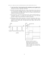
2.5.1 VISA/GPIB
Virtual Instrument Software Architecture (VISA) is a protocol used for communication
between a PC and external hardware. It includes serial communication through COM
ports and more specific I/O interfaces such as IEEE-488, or commonly known as General Purpose Interface Bus (GPIB), which was developed by Hewlett Packard for easier
interconnection with their instruments. In LabVIEW there are sub-VI’s for both VISA
and GPIB protocols. It is mostly up to the user which one to choose, since VISA includes GPIB communication as well, compare Figure 2.11 with Figure 2.12. However,
in National Instruments' NI-VISA user manual, they recommend using VISA sub-VI’s
for the entire system when programming multiple devices that communicate over more
than one bus-type [12]. Even Agilent technologies states on their website that it would
be better to use the more general VISA protocol instead of GPIB protocol.
13
Bachelor thesis: COMPLETION OF THE SOFTWARE REQUIRED FOR A HIGH-TEMPERATURE DLTS SETUP
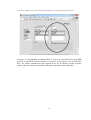
In Figure 2.11 the standard command *IDN? is sent to an external device using GPIB
protocol in LabVIEW and the response is read as a string shown in the box labelled
data. The *IDN?-command asks the targeted device for its identity and the response
string in this case contains information about the capacitance and conductance.
14
Bachelor thesis: COMPLETION OF THE SOFTWARE REQUIRED FOR A HIGH-TEMPERATURE DLTS SETUP
In Figure 2.12 the same command is sent to the same device as in Figure 2.11, but instead with VISA protocol in LabVIEW and the response is exactly the same. The
conclusion of this is that even though the external devices is connected with GPIB buses
to the PC, LabVIEW still can handle this with VISA VI’s. What is expected, since VISA
contains GPIB communication.
15
Bachelor thesis: COMPLETION OF THE SOFTWARE REQUIRED FOR A HIGH-TEMPERATURE DLTS SETUP
3 Method
3.1 Experimental setup
The instruments that were used in the experiments are listed in Table 3.1.
Device
Model
C-meter / C-V plotter
HP 4280A
Pulse generator
HP 8112A
Temperature controller
Tectra HC 3500 with Yudian AI 518P
(Programmable
artificial
intelligent
temperature controller)
The C-meter was used to measure the capacitance across the sample, the pulse generator
controlled the voltage pulses and with the temperature controller the temperature was
controlled and measured at the sample. The pulse generator and the C-meter was connected together in order to synchronize the measurements, so that no pulses was applied
across the sample during a capacitance read and no read of the capacitance was made
during a voltage pulse.
In order to control the instruments, they were all connected to a PC, on which a LabVIEW program had been constructed to perform DLTS measurements and collect data.
The DLTS control program had been built by a research group in Norway. Since they
were using another type of pulse generator and temperature controller which meant that
the control commands of those instruments were different and needed to be adjusted in
the LabVIEW program to fit the instruments at Ångström Laboratory. For the Yudian
controller a number of VI's had been created by the research group at Ångstöm Laboratory that contained most of the commands and functions needed for the DLTS main
program.
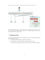
Figure 3.1 shows the hierarchy of the DLTS software with the main VI on top and its
sub-VI's below. The box at the bottom to the right contains the library of driver VI's for
Yudian's temperature controller.
16
Bachelor thesis: COMPLETION OF THE SOFTWARE REQUIRED FOR A HIGH-TEMPERATURE DLTS SETUP
A detailed description of most of the VI's in Figure 3.1, except the driver library for Yudian's temperature controller, can be found in A LabVIEW program for Deep-level
transient spectroscopy, by W. Liu [6].
3.2 Implementation
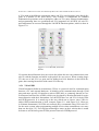
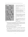
The front panel of the DLTS software is displayed in Figure 3.2 in which the following
parts are marked by circles:
A. The controls of the settings to initialize a measurement.
B. The path of the save file in which the measurement data is stored.
C. The indicators that displays the results of the measurements and the stop button.
17
Bachelor thesis: COMPLETION OF THE SOFTWARE REQUIRED FOR A HIGH-TEMPERATURE DLTS SETUP
3.2.1 Controls
The controls, shown in region A of Figure 3.2, are set before running the VI, because
when pushing run, the program reads the values of the controls and initializes the measurement with these settings. Of course, if anything goes wrong the stop button would
abort the program when pushed.
A closer view of the controls on the front panel is shown in Figure 3.3.
18
Bachelor thesis: COMPLETION OF THE SOFTWARE REQUIRED FOR A HIGH-TEMPERATURE DLTS SETUP
Figure 3.3: Controls of the DLTS
software
1
This specifies the COM-port to which the
temperature control is connected.
2
Sets the pulse generator's bias voltage,
see Figure 3.4.
3
Sets the pulse generator's pulse voltage,
see Figure 3.4.
4
When using an internal pulse set by the
C-meter this sets the bias voltage.
5
When using an internal pulse set by the
C-meter this sets the pulse voltage.
6
Sets the pulse width in ms, see Figure
3.4.
7
Minimum window length, in ms, sets the
first window's length, the next window
has automatically the double length of the
previous window, see Figure 3.5.
8
Sets the number of windows, see Figure
3.5.
9
This one is an indicator related to 7 It is
not controllable by the user, instead it
gets the value that is half of the min windowlength.
10 An indicator showing two to the power of
number of windows.
11 This sets the accuracy of the temperature at which a measurement can be made.
This relates to how well the PID parameters are set in the temperature controller,
i.e. a measurement is started when the temperature is within the interval of [TTemperature precision/2, T+ Temperature precision/2].
12 Start temp: the first temperature at which a measurement is made.
13 End temp: the last temperature at which a measurement is made.
14 Sets the increment step of the temperature.
15 Sets the number of scans per measurement, i.e. the number of scans per temperature. A measurement at a temperature is averaged over the number of scans in
order to reduce noise.
16 C-range is only active in the program when high resolution (20) is OFF. It tells
the C-meter in what range the capacitance is expected to be measured within. If
it is chosen too low, an overflow will occur and the data will be invalid. However, choosing a high value will reduce the accuracy of the measurement data.
19
Bachelor thesis: COMPLETION OF THE SOFTWARE REQUIRED FOR A HIGH-TEMPERATURE DLTS SETUP
17 C-speed specifies if the measurement of the capacitance is to be made in fast
mode or slow mode. As the names suggests fast mode provides optimum speed
but also less accuracy compared to slow mode.
18 Specifies the sample mode of how the C-meter will perform the data collection
of a measurement, In BURST mode the 4280A makes one measurement per
measurement point. In SAMPLE mode, however, it repeats several partial measurements at each measurement point.
19 This specifies the connection mode between the C-meter, the DUT and the external pulse generator, i.e. to which one of the inputs, slow or fast, the pulse
generator's output is connected and how the DUT is grounded.
20 With high resolution ON the capacitance is related to a capacitance offset, measured while in steady-state (the capacitance across the sample, with bias voltage
applied, after the transient has converged and become stable). When OFF the
offset is set to zero.
Figure 3.5: For point 7 & 8, Lock-in
function with three windows
displaying the minimum window
length and relation between the
window's lengths. The next following
window is always twice as large as the
current window.
20
Bachelor thesis: COMPLETION OF THE SOFTWARE REQUIRED FOR A HIGH-TEMPERATURE DLTS SETUP
3.2.2 Indicators
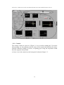
The indicators of the front panel are located in region C of Figure 3.2. Here follows a
description of some of the indicators.
The left transient of Figure 3.6 consists of raw data, called counts. It is the measured capacitance in binary coded format. Together with this data from the CV meter a status
byte is sent, which contains information of how to convert the capacitance data into values represented in Farads. In the right transient the raw data has been converted into
representation of pF.
Figure 3.7: Temperature indicators
of the front panel and the STOP
button
The content of Figure 3.7 can be found to the right of the transient indicators in the front
panel. It displays the SV (C), which is the set value of the temperature controller in degrees Celsius. Since the current temperature varied due to a bad PID parameter choice
of the temperature controller, it was interesting to see what the temperature was before
and after the measurement so that an understanding of how well the measurement was
made at wanted temperature could be done. In the figure the STOP button could also be
found, which aborts the program and finishes the current measurement at any point.
21
Bachelor thesis: COMPLETION OF THE SOFTWARE REQUIRED FOR A HIGH-TEMPERATURE DLTS SETUP
Figure 3.8: The measured capacitance
during the bias voltage as a function of
temperature
Figure 3.8 displays the steady-state capacitance, measured with a fixed reverse bias,
V bias , applied, at each temperature. Next to this indicator, to the right on the front panel,
is the measured conductance during the bias voltage (see Figure 3.2).
There are also indicators in the front panel which plots the DLTS signals using lock-in
and GS4 (which is not described in this thesis) weighting functions.
22
Bachelor thesis: COMPLETION OF THE SOFTWARE REQUIRED FOR A HIGH-TEMPERATURE DLTS SETUP
4 Results
After the basic GPIB communication VI’s had been replaced with VISA a successful
CV-measurement was made and is shown in Figure 4.1.
The measurement was made by sweeping a reverse voltage from 0V to -10V and measure the capacitance of the sample at room temperature. When applying a reverse voltage
across the sample the depletion region was expanded and the capacitance decreased
with proportion to the decreasing voltage as seen in Figure 4.1.
At the final step of this thesis a fully successful DLTS measurement was made using six
lock-in windows at 25ºC to 100ºC and is shown in Figure 4.2.
23
Bachelor thesis: COMPLETION OF THE SOFTWARE REQUIRED FOR A HIGH-TEMPERATURE DLTS SETUP
5 Discussion & Analysis
5.1 Communications
The first problem to solve was to understand why the communication with the devices
did not work. The only time they gave a response was when using NI MAX’s VISA test
panel, which allowed the user to send simple commands to the connected device in order to see if it responded. Since the VISA test panel used standard VISA commands to
write and read to the device, the problem seemed to be the GPIB VI’s in the LabVIEW
programs. All the GPIB VI’s were then replaced with VISA VI's instead, according to
Table A.1 in Appendix A, and the connected devices now gave responses even in LabVIEW. A successful CV measurement was then made at room temperature in order to
see that everything worked properly with the C-meter.
Later it was discovered that the GPIB card in the PC from Agilent technologies was not
compatible by default with National Instruments NI-488.2 protocol. But Agilent tech.
provided a configuration for enabling communication with NI-488.2 through their program Agilent Connection Expert that are included in Agilent IO Libraries Suite 16.3.
When enabling this, the GPIB VI's in LabVIEW started to work. Nevertheless VISA
VI's were still chosen to be used due to the recommendations from NI and Agilent and
the fact that it would be much easier to replace one of the instrument if the replacement
were using another type of communication.
5.2 Yudian control AI-518
The next step was to understand the heater and why it did not work in the DLTS program. The communication with the Yudian controller was made through a USB to serial
adapter and therefore VISA VI’s had to be used in LabVIEW. The first thing that was
added to the existing VI's for Yudian in the DLTS main program was a VISA CLOSE
function at the end of each VI’s execution to properly close the opened session for that
port. If the port is not closed it stays open for the task it was opened for and locked for
other uses. When this was done the communications with Yudian worked quite well.
However when a value was sent to Yudian to set a parameter, the answer could sometimes be ten times larger or ten times less than the wanted value. This was no fault,
merely an effect of how the Yudian controller was programmed to read and write data.
According to the datasheet of Yudian the response of all parameters with the same unit
as PV (process value) had to be divided by 10, when the dPt (decimal point) was set to
‘1’ or higher, in order to show the correct value. Also noticeable is that the written value
to a parameter with the same unit as PV had to be multiplied with 10 before sent to the
Yudian control to get the desired value correctly set. Just to make sure, most of the parameters were tested and processed accordingly so that it became user friendly, i.e. if the
user sent 10 to SP1 (setpoint 1), the Yudian control would interpret it as 10 and set SP1
24
Bachelor thesis: COMPLETION OF THE SOFTWARE REQUIRED FOR A HIGH-TEMPERATURE DLTS SETUP
to the same value.
All these changes led to quite a number of backup files and different versions of the Yudian VI’s. They were scattered in different directories on the computer which made
LabVIEW lose track of the ones that really mattered. Therefore, it was decided to collect the working and updated versions in a user specified driver and add it in the
LabVIEW palette for easy access whenever needed, thus preventing LabVIEW to link a
sub-VI to the wrong VI.
Later it was discovered that there were some values of some parameters that could not
be read in LabVIEW. Yudian did write the value correctly to the specified parameter, but
when trying to do a read of the same parameter value the answer from Yudian could not
be recognized as a true value by the computer. It was discovered that the received binary
bytes from Yudian sometimes contained the same value as what the termination character of the port was set to represent. This meant that when LabVIEW encountered the
value representing the termination character, LabVIEW thought that the reading was
done and therefore ended it, thus skipping the rest of the bytes. Realizing this, the solution was to disable the termination character and to change the property “Serial End
Modes for Reads” from default to “None(0)”, which meant that the read would not stop
when the termination character was encountered.
5.3 DLTS main VI
When all this was done, the Yudian VI's worked properly and put as a driver in the LabVIEW palette, it was time to see to the main DLTS VI. Since it originally came from a
group in Norway, who used a different setup with different brands and models for their
devices, some changes needed to be done in the main VI. It concerned the changing of
the instrument commands to the corresponding ones that could be applied to this setup.
When the commands had been changed, another problem was revealed. The Operating
System used by the computer was using Swedish standards, thus using a comma for
decimal mark, not point as of the English standard. This lead to parsing errors in the
devices, that used the English standard. By adding a format string in LabVIEW to every
written command the decimal mark was changed to be a point instead of a comma, but
just to make sure that every value in LabVIEW used point and not comma the change
were also made in the OS.
25
Bachelor thesis: COMPLETION OF THE SOFTWARE REQUIRED FOR A HIGH-TEMPERATURE DLTS SETUP
6 Summary & conclusions
Both NI and Agilent technologies recommend the users of GPIB and 488 protocols to
change to using the VISA protocol instead. The reason for this is, according to Agilent's
website, that Agilent 488 and NI-488.2 is proprietary libraries. Another reason would be
that it makes the program much more generalized. For example if a device is replaced
for one with another brand/model and the new uses another type of communication, it
will be much easier to make the change if the program is written using VISA VI's rather
than GPIB. Because, then the only thing that needs to be changed is the addresses of the
ports that are being used and perhaps correct the commands that is sent to the device.
As of this the main purpose of this thesis, to get the communication between LabVIEW
and the external instruments to work, was achieved and proved with the CV measurement, in Figure 4.1, and the DLTS measurement, in Figure 4.2.
6.1 Outlook
As for the future there are still some work with the DLTS software and making it more
user-friendly. A lot of the things can be updated in order simplify the code and make it
more effective. As for example wait until the temperature controller has reached and is
stable at its set point before entering the measurement loops. As well as remove the
high/low resolution choice and other controls that are not in use with the current setup,
so that no one gets confused about them being in the front panel. Or at least set them as
a constant in the block diagram in case if any of the instruments being replaced and the
controls then would be useful.
The hardware settings could also be considered for improvement. The PID parameters
of the temperature controller for example, could be better chosen in order to stabilize
the regulation and get it more accurate.
Other things that could be done is to implement more data acquisition functions such as
depth profiling and Arrhenius plots in order to analyse the results more easily. Even a
FAQ or manual could be most appropriate for future work and troubleshooting.
26
Bachelor thesis: COMPLETION OF THE SOFTWARE REQUIRED FOR A HIGH-TEMPERATURE DLTS SETUP
Appendix A
27
References
[1] H. J. von Bardeleben, J. C. Bourgoin, D. Deresmes, A. Huber and D. Stievenard,
Identification of a defect in a semiconductor, Phys. Rev. B 34, 7192 (1986)
[2] J. Isberg, et al. “High carrier mobility in single-crystal plasma-deposited
diamond.” Science 297.5587 (2002): 1670-1672.
[3] J-P. Colinge & C. A. Coolinge, Physics of Semiconductor Devices, Print ISBN: 14020-7018-7, eBook ISBN: 0-306-47622-3, (2002).
[4] S. M. Sze, Physics of Semiconductor Devices, ISBN 0-471-05661-8. Wiley. (1964)
[5] C. Kittel, Introduction to solid state physics, 7th edition, ISBN 0-471-11181-3.
Wiley. (1996)
[6] W. Liu, Master of Science Thesis: A LabVIEW program for Deep-level transient
spectroscopy, KTH, Stockholm (2009)
[7] S. Majdi, Master Thesis: Deep level transient spectroscopy investigation of silicon
carbide diodes, KTH, Stockholm (2005)
[8] B. Schumacher, H-G. Bach, P. Spitzer, J. Obrzut, Chapter 9: Electrical Properties
in Springer Handbook of Materials Measurement Methods, ISBN 978-3-54020785-6. Springer-Verlag Berlin Heidelberg, 2006, p. 431
[9] P. Pellegrino, Ph.D thesis: Point defects in ion-implanted silicon and silicon
carbide, KTH, Stockholm (2001).
[10] D. Åberg. Ph.D thesis: Capacitance Spectroscopy of Point Defects in Silicon and
Silicon Carbide, KTH, Stockholm (2001).
[11] H. Kortegaard Nielsen, Ph.D thesis: Capacitance Transient Measurements on
Point Defects in Silicon and Silicon Carbide, KTH, Stockholm (2005).
[12] VISA: NI-VISA user manual, 1996 (2001 edition), National Instruments
Corporation.
28