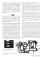
1
A forum for the exchange of circuits, systems, and software for real-world signal processing Li-Ion BATTERY CHARGING REQUIRES ACCURATE VOLTAGE SENSING (page 3) Quad-SHARC in CQFP—A 480-MFLOPS DSP Powerhouse (page 10) Ask the Applications Engineer—Capacitive Loads on Op Amps (page 19) Complete contents on page 3 Volume 31, Number 2, 1997 a THE AUTHORS Editor’s Notes NEW FELLOW We are pleased to note that Woody Beckford was introduced as the newest Fellow at our 1997 General Technical Conference. Fellow, at Analog Devices, represents the highest level of achievement that a technical contributor can achieve, on a par with Vice President. The criteria for promotion to Fellow are very demanding. Fellows will have earned universal respect and recognition from the technical community for unusual talent and identifiable innovation at the state of the art; their creative technical contributions in product or process technology will have led to commercial success with a major impact on the company’s net revenues. Their attributes include roles as mentor, consultant, entrepreneur, organizational bridge, teacher, and ambassador. They must also be effective leaders and members of teams and in perceiving customer needs. Woody’s technical abilities, accomplishments, and personal qualities well-qualify him to join Fellows Derek Bowers (1991), Paul Brokaw (1980), Lew Counts (1984), Barrie Gilbert (1980) Jody Lapham (1988), Fred Mapplebeck (1989), Jack Memishian (1980), Doug Mercer (1995), Mohammad Nasser (1993), Wyn Palmer (1991), Richie Payne (1994), Carl Roberts (1992), Paul Ruggerio (1994), Brad Scharf (1993), Mike Timko (1982), Bob Tsang and Mike Tuthill (1988), Jim Wilson (1993), and Scott Wurcer (1996). WOODROW BECKFORD A manufacturer of highperformance analog and mixedsignal products must be able rapidly and economically to test products meeting state-of-the-art specs in production quantities for market success and profitability. ADI’s Component Test Systems division specializes in designing and manufacturing advanced test systems to production-test our leadership products at low cost. Woody Beckford, the father of the latest series, the CTS-5000s, conceived the entire system architecture—hardware and software, designed the initial electrical and mechanical hardware, and directed the software development. The result, VXI-based testing with autocalibration (no trimming pots) and a loaded cost 1/3 the cost of anything comparable. But nothing comparable exists; many CTS-5000 capabilities, unavailable at any price, have been key to ADI’s continued leadership in high-speed converters. Woody was born and raised in Massachusetts and graduated from Northeastern University in 1982 with a BS in Physics. His co-op program jobs were at the MIT Bates Linear Accelerator (highenergy physics) and LTX Corporation (ATE). After graduation, he came to work for ADI’s CTS division. He has worked on just about every generation of CTS test equipment—the 2000, 3000, and 5000 series. In his spare time he enjoys amateur radio (N1IBY), listening to music, riding motorcycles, and target b shooting. He is married, with 3 children. [email protected] 2 Joe Buxton (page 3) is a Senior Design Engineer in Santa Clara, CA, for ADI’s Power Management product line. He is currently designing battery charger and switching regulator ICs. Previously he was an Applications Engineer, writing numerous articles and developing SPICE macromodels for ADI components. Joe has a BSEE (1988) from the University of California, Berkeley. In his leisure time, he enjoys running, skiing, reading, and travel. Mike Walsh (page 5) is a Senior Product Engineer in the HighSpeed Conver ter group, in Wilmington, MA, working on highresolution ADCs and mixed-signal consumer video ASICs. He joined Analog Devices in 1989, after graduating from Boston University with a MSEE. In his spare time, Mike enjoys woodworking and playing with his two daughters. Bob Scannell (page 10) is a Product Marketing Manager in the Multichip Products group of ADI, in Greensboro, NC. Bob has been involved with research, design, and marketing of DSP multiprocessors and multichip modules for 12 years. He holds a MS Computer Engineering degree from USC and a BSEE from UCLA. When away from work, Bob enjoys woodworking and travel. Grayson King (page 19), an Applications Engineer in the Central Applications group in Wilmington, MA, has a BSEE from Clarkson University. In addition to providing customer support for linear and converter products, Grayson is currently working to develop computer tools to aid designers in product selection. He also enjoys telemark skiing, white-water kayaking, and finding new ways to make a simple audio amplifier. [More authors on page 22] Cover: The cover illustration was designed and executed by Shelley Miles, of Design Encounters, Hingham MA. One Technology Way, P.O. Box 9106, Norwood, MA 02062-9106 Published by Analog Devices, Inc. and available at no charge to engineers and scientists who use or think about I.C. or discrete analog, conversion, data handling and DSP circuits and systems. Correspondence is welcome and should be addressed to Editor, Analog Dialogue, at the above address. Analog Devices, Inc., has representatives, sales offices, and distributors throughout the world. Our web site is http://www.analog.com/. For information regarding our products and their applications, you are invited to use the enclosed reply card, write to the above address, or phone 617-937-1428, 1-800-262-5643 (U.S.A. only) or fax 617-821-4273. ISSN 0161–3626 ©Analog Devices, Inc. 1997 Analog Dialogue 31-2 (1997) Li-Ion Battery Charging Requires Accurate Voltage Sensing New Battery Charger Controller Guarantees 61% Final Battery Voltage Accuracy by Joe Buxton Lithium-Ion (Li-Ion) batteries are gaining popularity for portable systems due to their increased capacity at the same size and weight as the older NiCad and NiMH chemistries. For example, a portable computer equipped with a Li-Ion battery can have a longer operating time than a similar computer equipped with a NiMH battery. However, designing a system for Li-Ion batteries requires special attention to the charging circuitry to ensure fast, safe, and complete charging of the battery. A new battery-charging IC, the ADP3810*, is designed specifically for controlling the charge of 1-to-4-cell Li-Ion batteries. Four highprecision fixed final battery-voltage options (4.2␣ V, 8.4␣ V, 12.6␣ V, and 16.8␣ V) are available; they guarantee the ± 1% final battery voltage specification that is so important in charging Li-Ion batteries. A companion device, the ADP3811, is similar to the ADP3810, but its final battery voltage is user-programmable to accommodate other battery types. Both ICs accurately control the charging current to realize fast charging at currents of 1 ampere or more. In addition, they both have a precision 2.0-V reference, and a direct opto-coupler drive output for isolated applications. Li-Ion Charging: Li-Ion batteries commonly require a constant current, constant voltage (CCCV) type of charging algorithm. In other words, a Li-Ion battery should be charged at a set current level (typically from 1 to 1.5 amperes) until it reaches its final voltage. At this point, the charger circuitry should switch over to constant voltage mode, and provide the current necessary to hold the battery at this final voltage (typically 4.2␣ V per cell). Thus, the charger must be capable of providing stable control loops for maintaining either current or voltage at a constant value, depending on the state of the battery. The main challenge in charging a Li-Ion battery is to realize the battery’s full capacity without overcharging it, which could result in catastrophic failure. There is little room for error, only ± 1%. Overcharging by more than +1% could result in battery failure, but undercharging by more than 1% results in reduced capacity. For example, undercharging a Li-Ion battery by only 100␣ mV (–2.4% for a 4.2-V Li-Ion cell) results in about a 10% loss in capacity. Since the room for error is so small, high accuracy is required of the charging-control circuitry. To achieve this accuracy, the controller must have a precision voltage reference, a low-offset high-gain feedback amplifier, and an accurately matched resistance divider. The combined errors of all these components must result in an overall error less than ± 1%. The ADP3810, combining these elements, guarantees the overall accuracy of ± 1%, making it an excellent choice for Li-Ion charging. Analog Dialogue 31-2 (1997) The ADP3810 and ADP3811: Figure 1 shows the functional diagram for the ADP3810/3811 in a simplified CCCV charger circuit. Two “gm” amplifiers (voltage input, current output) are key to the IC’s performance. GM1 senses and controls the charge current via shunt resistance, RCS, and GM2 senses and controls the final battery voltage. Their outputs are connected in an analog “OR” configuration, and both are designed such that their outputs can only pull up the common COMP node.Thus, either the current amplifier or the voltage amplifier is in control of the charging loop at any given time. The COMP node is buffered by a “gm” output stage (GM3), the output current of which directly drives the dcdc converter control input (via an opto-coupler in isolated applications). VBAT VIN OUT DC/DC CONVERTER RETURN GND CTRL IN ICHARGE RCS VRCS BATTERY 2.0V 0.1mF 0.1mF R3 ADP3811 ONLY R1 R2 VCC VCS VREF UVLO 1.5MV 80kV VCTRL VREF VSENSE ADP3810 ONLY R1 UVLO R2 GM1 VREF BUFFER GM2 UVLO IOUT 200V ADP3810/ ADP3811 OUT GM3 100mA 1.2V COMP GND CC RC Figure 1. Block diagram of the ADP3810/3811 in a simplified batter y-charging circuit. The ADP3810 includes precision thin-film resistors to divide down the battery voltage accurately and compare it to an internal 2.0-V reference. The ADP3811 does not include these resistors, so the designer can program any final battery voltage with an external resistor pair according to the formula below. A buffer amplifier provides a high-impedance input to program the charge current using the VCTRL input, and an under voltage lock-out (UVLO) circuit ensures a smooth start-up. R V BAT = 2.000 V × 1+ 1 R2 IN THIS ISSUE Volume 31, Number 2, 1997, 24 Pages Editor’s Notes (New Fellow: Woody Beckford), Authors, . . . . . . . . . . . . . ␣ 2 Li-Ion battery charging requires accurate voltage sensing . . . . . . . . . . . . . . . . ␣ 3 Pin-compatible 14-bit monolithic ADCs: First to sample from 1-10 MSPS (AD924x) 5 200-MHz 16␣ ×␣ 16 video crosspoint switch IC (AD8116) . . . . . . . . . . . . . . . ␣ 6 Selecting mixed-signal components for digital communications systems (IV) . . . ␣ 7 Quad-SHARC DSP in CQFP—a 480-MFLOPS powerhouse (AD14060) . 10 Digital signal processing 101—an introductory course in DSP system design—II . . 11 New-Product Briefs: ADCs and DACs, R-DAC, Audio Playback . . . . . . . . . . . . . . . . . . . . 15 Amplifiers, Mux, Reference, DC-DC . . . . . . . . . . . . . . . . . . . . . . . . . 16 Power Management, Supervisory Circuits . . . . . . . . . . . . . . . . . . . . . 17 Temp Sensor, Codec, Communications & ATE ICs . . . . . . . . . . . . . . 18 Ask The Applications Engineer—25: Op amps driving capacitive loads . . . 19 Worth Reading, More authors . . . . . . . . . . . . . . . . . . . . . . . . . . . . . . . . 22 Potpourri . . . . . . . . . . . . . . . . . . . . . . . . . . . . . . . . . . . . . . . . . . . . . . . 23 3 To understand the “OR” configuration, assume that a fully discharged battery is inserted in the charger. The voltage of the battery is well below the final charge voltage, so the VSENSE input of GM2 (connected to the battery) brings the positive input of GM2 well below the internal 2.0-V reference. In this case, GM2 wants to pull the COMP node low, but it can only pull up, so it has no effect at the COMP node. Since the battery is dead, the charger starts to increase the charge current and the current loop takes control.The charge current develops a negative voltage across the 0.25-Ω current-shunt resistor (RCS). This voltage is sensed by GM1 through the 20-kΩ resistor (R3). At equilibrium, (ICHARGER CS)/R3 ␣ =␣ –VCTRL /80␣ kΩ. Thus the charge current is maintained at specifications of the charger are controlled by the ADP3810/3811, which guarantees the final voltage within ± 1%. The current drive of the ADP3810/3811’s control output directly connects to the photo-diode of an opto-coupler with no additional circuitry. Its 4-mA output current capability can drive a variety of opto-couplers—an MOC8103 is used here. The current of the photo-transistor flows through RF, setting the voltage at the 3845’s COMP pin and thus controlling the PWM duty cycle. The controlled switching regulator is designed so that increased LED current from the opto-coupler reduces the duty cycle of the converter. While the signal from the ADP3810/3811 controls the average charge current, the primary side should have a cycle by cycle limit of the switching current. This current limit has to be designed such that, with a failed or malfunctioning secondary circuit or opto-coupler, or during start up, the primary power circuit components (the FET and transformer) won’t be over-stressed. When the secondary side VCC rises above 2.7␣ V, the ADP3810/ 3811 takes over and controls the average current. The primary side current limit is set by the 1.6-Ω current sense resistor connected between the power NMOS transistor, IRFBC30, and ground. V CTRL R3 80 k Ω RCS If the charge current tends to exceed the programmed level, the VCS input of GM1 is forced negative, which drives the output of GM1 high. This in turn pulls up the COMP node, increasing the current from the output stage, reducing the drive of the dc/dc converter block (which could be implemented with various topologies such as a flyback, buck, or linear stage), and finally, reducing the charge current. This negative feedback completes the charge current control loop. I CHARGE = The ADP3810/3811, the core of the secondary side, sets the overall accuracy of the charger. Only a single diode is needed for rectification (MURD320) and no filter inductor is required. The diode also prevents the battery from back driving the charger when input power is disconnected. A 1000-µF capacitor (CF1) maintains stability when no battery is present. RCS senses the average current (see above), and the ADP3810 is connected directly (or ADP3811 through a divider) to the battery to sense and control its voltage. As the battery approaches its final voltage, the inputs of GM2 come into balance. Now GM2 pulls the COMP node high and the output current increases, causing the charge current to decrease, maintaining VSENSE and VREF equal. Control of the charging loop has changed from GM1 to GM2. Because the gain of the two amplifiers is very high, the transition region from current to voltage control is very sharp, as Figure 2 shows. This data was measured on a 10-V version of the off-line charger of Figure 3. With this circuit, a complete off-line Li-Ion battery charger is realized. The flyback topology combines an AC/DC converter with the charger circuitry to give a compact, low-cost design. The accuracy of this system depends on the secondary side controller, the ADP3810/3811. The device’s architecture also works well in other battery charging circuits. For example, a standard dc-dc buck type of charger can easily be designed by pairing the an ADP3810 and an ADP1148. A simple linear charger can also be designed with just the ADP3810 and an external pass transistor. In all cases, the inherent accuracy of the ADP3810 controls the charger and guarantees the ± 1% final battery voltage needed for Li-Ion b charging. Complete Off-Line Li-Ion Charger: Figure 3 shows a complete charging system using the ADP3810/3811. This off-line charger uses the classic flyback architecture to create a compact, low cost design. The three main sections of this circuit are the primaryside controller, the power FET and flyback transformer, and the secondary-side controller. This design uses an ADP3810, directly connected to the battery, to charge a 2-cell Li-Ion battery to 8.4␣ V at a programmable charge current from 0.1 to 1␣ A.The input range is from 70␣ to␣ 220␣ V␣ ac—for universal operation. The primary side pulsewidth modulator used here is the industry-standard 3845, but other PWM components could be used. The actual output 1.0 10nF 1N4148 100V VCTRL = 1.0V 0.9 ILIMIT 0.6 VOUT AC 120/220V– 0.4 CF1 1mF 100kV 1N4148 22nF L VCTRL = 0.5V 0.5 1A 47mF 13V MURD320 N 0.2 VCC VCTRL = 0.125V COMP 0.1 RF 3.3kV 2 3 4 5 6 7 VOUT 8 9 10 CF 1nF 3.3kV * 1% TOLERANCE ** TX1 f = 120kHz LPR = 750mH LSEC = 7.5mH 0.1mF 10kV 0.1mF 1kV 1.6V VCS GND VREF VCC VSENSE ADP3810/ADP3811 0.1mF OUT 2.2nF MAXIMUM VOUT = 8.4V CHARGE CURRENT 0.1A TO 1A ISENSE 470pF RT/CT RCS 0.25V* IRFBC30 OUTPUT VREF Figure 2. Current/Voltage Transition of the ADP3810 CCCV Charger BATTERY CC2 RC2 0.2mF 300V 10V PWM 3845 VFB 11 R4 1.2kV R3 20kV* 330pF 330V VCTRL = 0.25V 0.3 0 TX1** 9.1V 3W 0.7 CF2 220mF 22mF 50mF/450V 0.8 3.3V COMP 3.3kV RC1 10kV VCTRL GND CHARGE CURRENT CONTROL 0.1mF VOLTAGE CC1 1mF OPTO COUPLER MOC8103 *For technical data, consult our Web site, www.analog.com, use Faxback (see p. 24). 4 Figure 3. Complete Off-Line Li-Ion Battery Charger Analog Dialogue 31-2 (1997) by Mike Walsh, Larry Singer, and Joe DiPilato The AD924x family are the industry’s first monolithic 14-bit analog-to-digital converters (ADCs) to exceed a 1-MHz sample rate. The three pin-compatible devices in MQFP-44 packages, AD9240, AD9243, and AD9241 are specified at 10, 3, and 1.25MHz clock rates, respectively. With their 12-bit counterparts, the AD9220/23/21 family, they form a complete set of highperformance CMOS A/D converter solutions.* The monolithic single-supply AD924x series of converters at last offer the benefits of high performance, accompanied by significant savings of cost, power, and board space. The assembled hybrids and modules that they will supplant cost many hundreds of dollars, dissipate watts of power, and are typically packaged in large 24pin DIPs; they operate from a minimum of two supplies and are usually specified for the 0 to 70°C commercial temperature range. The AD924x family is 5 to 20 times less costly in price and power than a popular family of competitive hybrids, are smaller, and have better dynamic specifications. The table lists some of the key specifications of the AD924x family [SNR (signal-to-noise ratio), SINAD (signal to noise & distortion), THD (total harmonic distortion) and SFDR (spurious-free dynamic range)].The devices operate from a single 5-V supply and have the low power dissipation shown. AD9240 AD9243 AD9241 Update rate (MSPS) 10 3 1.25 AIN frequency (kHz) 500 500 500 SNR (dB typ/min) 78.5/76 80/77 79/75.5 SINAD (dB typ/min) 77.5/75 79/76 78/74.5 THD (dB typ/max) –85/–77 –87/–80 –88/–77.5 SFDR (dB typ) 90 91 88 Power dissipation (W max) 0.33 0.145 0.085 Price ($US, 100s) $74.95 $49.95 $21.50 Their high performance, low power, and low price are of particular relevance in emerging and next-generation consumer applications, such as communications and imaging. They will be used in cellular and PCS basestations, ADSL/HDSL modems, flatbed and drum document scanners, film and x-ray scanners, infra-red and medical imagers. For communications, wide input bandwidth, low distortion & wide dynamic range, and low power are major attractions. Wide dynamic range helps to reduce gain requirements in the receiver IF strip. High input bandwidth allows the AD924x family to be used in undersampling applications to perform IF to baseband downconversion/mix-down. For imaging, their low noise, 14-bit nomissing code, and SNR performance are key. In addition, infra-red *For technical data, consult our Web site, www.analog.com, use Faxback (see p. 24). Analog Dialogue 31-2 (1997) VINA DAC-AMP1 G1 = 16 SHA VINB F1 1V 5 DAC-AMP2 G2 = 8 F2 5 DAC-AMP3 G3 = 8 F3 4 4 VREF F4 4 4 4 DIGITAL CORRECTION LOGIC REF 14 DOUT SENSE Figure 1. 14-bit pipelined ADC architecture. The converter’s overall DC accuracy (INL, DNL) largely depends on the accuracy of the first pipeline stage, which is limited by capacitor mismatch. By converting 5 bits in the first pipeline stage, the effects of capacitor mismatch are sufficiently suppressed to achieve 14-bit accuracy without the need for on-chip calibration. Integral and differential nonlinearity are typically ± 2.5 and ± 0.6␣ LSB, respectively. The dynamic and noise performance of the A/D are largely determined by performance of the input SHA, which was carefully optimized to provide low noise and distortion over a moderately wide bandwidth. Typical input-referred noise is 0.36␣ LSB, or 110␣ µV␣ rms. Figure 2 compares typical S/(N+D) and total harmonic distortion (THD) as a function of input frequency for the three devices at their specified sampling rates. These plots demonstrate superior dynamic performance well beyond the devices’ respective Nyquist frequencies. 85 –45 SIGNAL-TO-NOISE PLUS DISTORTION 80 AD9240 –50 75 –55 AD9243 AD9241 70 –60 –65 65 –70 60 AD9241 55 50 –75 AD9243 AD9240 TOTAL HARMONIC DISTORTION –80 –85 45 40 0.01 0.1 1 FREQUENCY – MHz 10 TOTAL HARMONIC DISTORTION – dB 1.25 to 10␣ MSPS pin-compatible AD924xs enable new applications in communications and imaging SIGNAL-TO-NOISE PLUS DISTORTION – dB 14-Bit Monolithic ADCs: First to Sample Faster than 1␣ MSPS imaging applications benefit from low power dissipation (heat generation); the ADC can reside closer to the IR sensor. Yet other applications for high performance, low power, and low price include: instrumentation, radar, collision-avoidance systems, test equipment, signal analysis, and data acquisition. Like many high speed converters offered by Analog Devices, the AD924x series is based on a multibit, pipelined architecture, but it is implemented in low-power switched-capacitor circuitry. Figure 1 shows a block diagram of the complete ADC. A low-noise, wideband sample-hold amplifier (SHA) with differential outputs precedes the pipelined core, and accepts single-ended or differential inputs up to 5␣ V␣ p-p. From the SHA’s output, the signal path is fully differential. The first pipeline stage converts the 5␣ most significant bits and amplifies the remainder, or residue, for successive conversions by the next three 4-bit stages. The results of these partial conversions by the four pipeline stages are then time-aligned and added (with one bit of overlap) to obtain the final 14-bit result. Each clock cycle produces a new conversion, with 3-cycle latency. –90 100 Figure 2. SINAD and THD vs. Signal Frequency The on-chip bandgap voltage reference can be pin-strapped to 1␣ V or 2.5␣ V, or set for any voltage in between using an external resistor divider. Optionally, an external voltage reference may be used. The AD924x family, packaged in a 44-pin MQFP, operates over the –40 to +85°C extended industrial temperature range. b 5 200-MHz 16316 Video Crosspoint Switch IC AD8116 has buffered outputs and inputs, 0.01%/0.018 Differential Gain/Phase Error The AD8116* is a wideband 256-point analog switch with 16 highimpedance inputs and 16 buffered outputs. With this “nonblocking” type of crosspoint switch, any input signal can be routed to one or more (including all) of the outputs, as programmed via an 80-bit serial word (Figure 1). pins. The 80 bits of switching data are coded in 16 5-bit groups, associated with each of the outputs, starting with OUT15. The first bit indicates whether the output is enabled or disabled, and the last four indicate the input to which it is connected. After the shift register is filled with the 80 bits of new control data, the data is transferred to the parallel switch control latches, where it resides until updated or the power is turned off. . CLK DATA IN CLK 80-BIT SHIFT REG. DATA OUT UPDATE UPDATE 80 CE CE EXAMPLE: FIRST 6 INPUTS AND OUTPUTS IN1 IN2 IN3 IN4 IN5 IN6 IN1 IN2 IN3 IN4 IN5 IN6 RESET OUT1 & OUT3 OUT6 NC OUT2 OUT4 OUT5 AD8116 RESET 80 16 DECODE 16 × 5:16 DECODERS 256 SET INDIVIDUAL OR RESET ALL OUTPUTS TO "OFF" OUTPUT BUFFER +1 +1 OUT2 OUT3 OUT4 OUT5 OUT6 OUT1 PARALLEL LATCH WHEN THIS SWITCH CELL IS ACTIVATED, IT CONNECTS IN2 TO OUT6 +1 +1 +1 Figure 1. Non-blocking crosspoint switching. +1 The individual output buffer amplifiers can drive 150-Ω video loads with 0.01% differential gain and 0.01° differential phase errors, and with flat response (to within 0.1␣ dB) to 60␣ MHz (200␣ MHz for –3␣ dB). Each output has an independent Disable feature to permit cascading of multiple AD8116s to build larger switch arrays. This complete 256-point solution is offered in a tiny 128-lead TQFP (5/8"␣ ×␣ 5/8") and consumes only 90␣ mA of supply current. It can be used alone or in groups, with daisy-chained serial data, to expand the numbers of paths to over 200 inputs and/or outputs. Figure 2 shows the scheme of input and output connections for a 48␣ ×␣ 48 array architecture, using 9 AD8116s. In addition, the serial control data is daisy-chained from DATA OUTs to DATA INs. IN 0–15 IN 16–31 IN 32–47 16 16 16 AD8116 AD8116 AD8116 IN IN IN OUT OUT OUT AD8116 AD8116 AD8116 IN IN IN OUT OUT OUT AD8116 AD8116 AD8116 IN IN IN OUT 16 OUT 0–15 OUT OUT 16 OUT 16–31 16 OUT 32–47 Figure 2. 48␣ ×␣ 48 crosspoint (2,304-point) array. Video crosspoint switches are used primarily for routing high-speed signals, including composite video (NTSC, PAL, SECAM, etc.), component video (YUV, RGB, etc.), in applications such as studios, video-on-demand, in-flight entertainment, and surveillance and video-teleconferencing. Figure 3 is a functional block diagram of the AD8116. Note the inputs, switch matrix, set of output buffers, individually controlled 3-state enable/disable switches, and the DATA IN and DATA OUT 16 INPUTS SWITCH MATRIX +1 +1 +1 ENABLE/DISABLE +1 16 OUTPUTS +1 +1 +1 +1 +1 +1 Figure 3. AD8116 functional block diagram. The switch channels can be used individually to switch high-density single-ended composite video signals or paired to handle differential signals. So a single AD8116 can form an 8␣ ×␣ 8 differential crosspoint switch. For RGB orYUV data, three channels can be used for each video channel. Crosstalk is less than –70␣ dB, with –105␣ dB of isolation, at 5␣ MHz. The output buffers, when disabled, are at high impedance. This permits outputs of multiple AD8116s to be paralleled with minimal loading of the on channel. In expanded configurations, (for example the 48␣ ×␣ 48 array of Figure 2), the inputs associated with a given range of outputs are paralleled and the outputs are wire-OR’d together. Of course, arrays need not be square (for example 128␣ ×␣ 16). The AD8116JST is specified for ± 5-V power supplies and for operation at temperatures from 0 to 70°C. It dissipates 900␣ mW (3.5␣ mW per switch point). Housing is in a 14␣ mm␣ ×␣ 14␣ mm 128lead plastic TQFP. A 4-layer evaluation board (AD8116EB) is available to demonstrate the device’s performance; the board is available as a fully populated design-in kit, with BNC-type connectors, plus custom cable, Windows™-based software for control via a PC printer port, and board layout files. Price of the AD8116JST is $90 in 1000s, and the AD8116-EB design-in kit is b priced at $395. *For technical data, consult our Web site, www.analog.com, use Faxback (see p. 24). 6 Analog Dialogue 31-2 (1997) Selecting Mixed Signal Component for Digital Communications Systems IV. Receiver Architecture Considerations by Dave Robertson Part I introduced the concept of channel capacity and its dependence on bandwidth and SNR; part II summarized briefly different types of modulation schemes; and part III discussed approaches to sharing the communications channel, including some of the problems associated with signal-strength variability. This installment considers some of the architectural trade-offs used in digital communications receiver design for dealing with dynamic range management and frequency translation problems. TRANSMIT POWER POWER System Constraints: In a digital communications system, the function of the receiver circuitry is to recover the transmitted signal and process it for introduction to the demodulator, which then recovers the digital bits that constitute the transmitted message. As the last installment illustrates, obstacles to signal recovery show up as the signal travels through the transmission medium. These “impairments” can include signal attenuation, reflections, distortion, and the introduction of “interferers” (other signals sharing the transmission medium). The nature of the transmission impairments is a strong function of the medium (wireless, coaxial cable, or twisted pair wire), the communications scheme being used (TDMA, FDMA, CDMA, etc.) and the particular circumstances of the transmitter/receiver pair (distance, geography, weather, etc.). In any event, the important receiver design considerations are present to some extent in all receivers, simply to differing degrees. For this discussion, two examples will be used to illustrate the various receiver design issues. Figure 1 illustrates the relevant portions of the signal spectrum at the transmitter outputs and receiver inputs for two very different systems: a GSM cellular telephony application (Figure 1a and 1b) and an ADSL twisted-pair modem application (Figure 1c and 1d). 901.0 FREQUENCY – MHz 1.1M 100k FREQUENCY – Hz a.␣ Cellular transmission. c.␣ ADSL transmission. DESIRED SIGNAL RECEIVE 900 901.0 902 FREQUENCY – MHz b.␣ Cellular received signal. POWER POWER INTERFERERS ECHO 100k 1.1M FREQUENCY – Hz d.␣ ADSL received signal. Figure 1. Transmitted and received spectra. GSM uses a combination of FDMA (frequency division multiple access) and TDMA (time division multiple access) for multiplexing and a variation of quadrature phase shift keying for modulation. Analog Dialogue 31-2 (1997) In 1b, the amplitude is significantly reduced—a result of distance from the transmitter. In addition, several strong interfering signals are present—signals from other cellular transmitters in nearby bands that are physically closer to the receiver than the desired transmitter. The ADSL modem in this example (Figure 1c) uses FDMA to separate upstream and downstream signals, and transmits its signal in a number of separate frequency bins, each having its own QAM (quadrature amplitude modulation) constellation (discrete multitone, or DMT modulation). The ADSL signal is attenuated by the twisted pair wire; attenuation is a strong function of frequency. In addition, an “interferer” is present. This might seem anomalous in a dedicated wire system, but in fact the interferer is the duplex (travelling in the opposite direction) signal of the modem leaking back into the receiver. This is generally referred to as near-end echo, and for long lines it may be much stronger than the received signal (Figure 1d). These two examples illustrate critical functions of the receiver processing circuitry: Sensitivity represents the receiver’s ability to capture a weak signal and amplify it to a level that permits the demodulator to recover the transmitted bits. This involves a gain function. As was discussed in Part 3 of this series, signal strength may vary significantly, so some degree of variable or programmable gain is generally desired. The way gain is implemented in a receiver usually requires a tradeoff between noise, distortion, and cost. Low-noise design dictates that gain be implemented as early in the signal chain as possible; this is a fundamental principle of circuit design. When calculating the noise contribution from various noise sources in a system, the equivalent noise of each component is referred to one point in the system, typically the input—referred-to-input (RTI) noise. The RTI noise contribution of any given component is the component’s noise divided by the total signal gain between the input and the component. Thus, the earlier the gain occurs in the signal path, the fewer stages there are to contribute significant amounts of noise. Unfortunately, there are obstacles to taking large amounts of gain immediately. The first is distortion. If the signal is in the presence of large interferers (Figures 1b, 1d), the gain can’t be increased beyond the point at which the large signal starts to produce distortion. The onset of distortion is described by a variety of component specifications, including THD (total harmonic distortion), IP3 (third-order intercept point: a virtual measurement of the signal strength at which the power of the 3rd-order distortion energy of the gain stage is as strong as the fundamental signal energy), IM3 (a measure of the power in the 3rd order intermodulation products), and others. For an A/D converter or digital processing, “clipping” at full-scale produces severe distortion. So these strong signals must usually be attenuated before all the desired gain can be realized (discussed below). Cost is another limiting factor affecting where gain can occur in the signal chain. As a general rule of thumb, high-frequency signal processing is more expensive (in dollars and power) than low frequency or baseband signal processing. Hence, systems that include frequency translation are generally designed to try to implement as much of the required gain as possible at the IF or baseband frequencies (see below). Thus, to optimize the location of gain in the signal path, one must simultaneously trade off the constraints of noise, distortion, power dissipation, and cost. 7 Specifications used to evaluate gain stages include the gain available (linear ratio or dB) and some description of the noise of the component, either in RTI noise spectral density (in nV/√Hz) or as noise figure (basically, the ratio of the noise at the output divided by the noise at the input, for a given impedance level). Selectivity indicates a receiver’s ability to extract or select the desired signal in the presence of unwanted interferers, many of which may be stronger than the desired signals. For FDMA signals, selectivity is achieved through filtering with discrimination filters that block unwanted signals and pass the desired signal. Like gain, filtering is generally easier at lower frequencies. This makes intuitive sense; for example, a 200-kHz bandpass filter implemented at a 1-MHz center frequency would require a much lower Q than the same 200-kHz filter centered on 1␣ GHz. But filtering is sometimes easier in certain high-frequency ranges, using specialized filter technologies, such as ceramic or surface acoustic wave (SAW) filters. As noted above, filtering will be required early in the signal path to attenuate the strong interferers. Such filters will need to combine the required frequency response and low noise. Figures of merit for a filter include bandwidth, stop-band rejection, pass-band flatness, and narrowness of the transition band (the region between pass-band and stop-band). Filter response shape will largely be determined by the channel spacing and signal strength variations of the communications channel. Most FDMA cellular standards seek to ease filter requirements by avoiding the use of adjacent frequency channels in the same or adjacent cells, to permit wider transition bands and lower-Q (cheaper) filters. Part of the selectivity problem is tuning—the ability to change the desired channel, since in most applications the signal of interest could be in any one of a number of available frequency bands. Tuning may be accomplished by changing the filter bandpass frequencies, but it is more commonly realized as part of the mixing operation (see below). Frequency planning (mixing): Radio frequencies are selected based on radio transmission characteristics and availability of bandwidth for use for a given service, such as FM radio or cellular telephony. As was noted earlier, signal processing at high radio frequencies tends to be expensive and difficult. Besides, this added trouble seems unnecessary, since in most cases the actual signal bandwidth is at most a few hundred kHz. So most radio receivers use frequency translation to bring the signal carriers down to lower, more manageable frequencies for most of the signal processing.The most common means of frequency translation is a mixer (Figure 2). WHATEVER IS HERE ENDS UP IN IF TOO LOCAL OSCILLATOR IF FREQUENCY RF + IMG INPUT IMAGE BAND LO TARGET SIGNAL IF – RF ( LO LO + RF ( LO – IMG LO + IMG Figure 2. Mixing—the image problem. Mixing means using a nonlinear operation, usually multiplying the input signal and a reference oscillator signal, to produce spectral images at the sum and difference frequencies. For example: if we “mix” an RF signal at 900 MHz with an oscillator at 890 MHz, the output of the mixer will have energy at 1790 MHz (sum of frequencies) and 10␣ MHz (their difference). The 10-MHz signal becomes the signal of interest at the 10-MHz intermediate frequency (IF), while the sum frequency is easily filtered out. If the oscillator 8 frequency is increased to 891␣ MHz, it will translate an RF signal at 901␣ MHz to the IF; hence, channel selection, or tuning, can be realized by varying the oscillator frequency and tuning the output to the IF, using a fixed-frequency bandpass filter. However, when mixing the 900-MHz RF with an 890-MHz local oscillator (LO), any 880-MHz interference present on the RF signal will also be translated to a difference frequency of 10␣ MHz. Clearly, any RF signal at the “image” frequency of 880␣ MHz must be suppressed well below the level of the desired signal before it enters the mixer. This suggests the need for a filter that passes 900␣ MHz and stops 880␣ MHz, with a transition band of twice the intermediate frequency. This illustrates one of the trade-offs for IF selection: lower IFs are easier to process, but the RF image-reject filter design becomes more difficult. Figures of merit for mixers include gain, noise, and distortion specifications like those used for gain stages, as well as the requirements on the oscillator signal input. Other mechanisms of dealing with the image rejection problem are beyond the scope of this short treatment. One worth mentioning, though, because of its widespread use is quadrature downconversion. In-phase and quadrature representations of the input signal are mixed separately and combined in a way to produce constructive interference on the signal of interest and destructive interference on the unwanted image frequency. Quadrature mixing requires two (or more) signal processing channels well-matched in both amplitude and frequency response, because mismatches allow the unwanted image signal to leak into the output. Equalization: Real-world transmission channels often have a more severe impact on signals than simple attenuation. Other channel artifacts include frequency-dependent amplitude and phase distortion, multi-path signal interference (prevalent in mobile/cellular applications), and bandlimiting/intersymbol interference from the receiver processing circuits. Many receiver systems feature “equalization” circuits, which provide signal processing that attempts to reverse channel impairments to make the signal more like the ideal transmitted signal. They can be as simple as a high frequency boost filter in a PAM system or as complicated as adaptive time- andfrequency-domain equalizers used in DMT ADSL systems. As capacity constraints push system architectures towards more complicated modulation schemes, equalization techniques, both in the analog and digital domains, are increasing in sophistication. Diversity: In mobile applications, the interference patterns from a mobile transmitter can vary the strength of the signal at the basestation receiver, making the signal difficult or impossible to recover under certain conditions. To help reduce the odds of this occurring, many basestations are implemented with two or more receiving antennas separated by a fraction of the RF wavelength, such that destructive interference at one antenna should represent constructive interference at the other. This diversity improves reception at the cost of duplicating circuitry. Diversity channels need not be closely matched (matching is required for quadrature channels), but the system must have signal processing circuitry to determine which of the diversity paths to select. Phased-array receivers take the diversity concept to the ultimate, combining the signal from an array of receivers with the proper phase delays to intentionally create constructive interference between the multiple signal paths, thereby improving the receiver’s sensitivity. Conventional Receiver Design: Figure 3a illustrates a possible architecture for a GSM receiver path, and Figure 3b illustrates that of an ADSL modem. As noted earlier, the task of the receive Analog Dialogue 31-2 (1997) circuitry is to provide signal conditioning to prepare the input signal for introduction to the demodulator. Various aspects of this signal conditioning can be accomplished with either digital or analog processing. These two examples illustrate fairly traditional approaches, where the bulk of signal processing is done in the analog domain to reduce the performance requirements on the A/D converter. In both examples, the demodulation itself is done digitally. This is not always necessary; many of the simpler modulation standards can be demodulated with analog blocks. However, digital demodulation architectures are becoming more common, and are all but required for complicated modulation schemes (like ADSL). The GSM receiver signal path shown in Figure 3a illustrates the use of alternating gain and filter stages to provide the required selectivity and sensitivity. Channel selection, or tuning, is accomplished by varying the frequency of the first local oscillator, LO1.Variable gain and more filtering is applied at the IF frequency. This is a narrowband IF system, designed to have only a single carrier present in the IF processing. The IF signal is mixed down to baseband, where it is filtered once more and fed to a sigmadelta A/D converter. More filtering is applied in the digital domain, and the GMSK signal is digitally demodulated to recover the transmitted bit stream. The ADSL receiver has different requirements. Frequency translation is not required, since the signal uses relatively low frequencies (dc to 1.1␣ MHz). The first block is the “hybrid”, a special topology designed to extract the weak received signal from the strong transmitted signal (which becomes an interferer—see Figure 1d). After a gain stage, a filter attempts to attenuate the echo (which is in a different frequency band than the desired signal.) After the filter, a variable-gain stage is used to boost the signal to as large a level as possible before it is applied to the A/D converter for digitization. In this system, equalization is done in both the time and frequency domains before the signal is demodulated. This example shows the equalization taking place digitally (after the A/D converter), where it is easier to implement the required adaptive filters. New twists—receivers “go digital”: Advances in VLSI technology are making more-sophisticated receiver architectures practical; they enable greater traffic density and more flexibility— even receivers that are capable of handling multiple modulation standards. An important trend in this development is to do more and more of the signal processing in the digital domain. This means that the A/D “moves forward” in the signal chain, closer to the BASEBAND FILTERING ADC RF FILTER IF FILTER 90° TUNED LOCAL OSCILLATOR LO1 FIXED LOCAL OSCILLATOR VARIABLE GAIN DEMODULATOR ADC FIXED GAIN a.␣ GSM receiver. TRANSMIT SIGNAL ADAPTIVE DIGITAL EQUALIZER ADC FILTER VARIABLE GAIN FILTER DEMODULATOR b.␣ ADSL modem receiver. antenna. Since less gain, filtering and frequency translation is done prior to the A/D, its requirements for resolution, sampling frequency, bandwidth, and distortion increase significantly. An example of this sophistication in modems is the use of echo cancellation. The spectrum of Figure 1d shows the strong interferer that dominates the dynamic range of the received signal. In the case of a modem, this interference is not a random signal, but the duplex signal that the modem is transmitting back upstream. Since this signal is known, signal processing could be used to synthesize the expected echo on the receive line, and subtract it from the received signal, thereby cancelling its interference. Unfortunately, the echo has a strong dependence on the line impedance, which varies from user to user— and even varies with the weather. To get reasonable cancellation of the echo, some sort of adaptive loop must be implemented. This adaptivity is easier to do in the digital domain, but it requires an ADC with sufficient dynamic range to simultaneously digitize the weak received signal and the echo; in the case of ADSL, this suggests a 16 bit A/D converter with 1.1␣ MHz of bandwidth. (e.g., the AD9260). As a significant reward for this higher level of performance with a sufficiently accurate echo canceller, upstream and downstream data can simultaneously occupy the same frequencies, dramatically increasing the modem’s capacity, particularly on long lines. In the case of GSM, there are various approaches to advanced receivers. As the ADC moves forward in the signal chain, instead of capturing a baseband signal around dc, it has to digitize the IF signal, which would typically be in the range of 70␣ MHz to 250␣ MHz. Since the bandwidth of interest is only a few hundred kHz, it is unnecessary (and undesirable) to run the ADC at 500␣ MHz; instead, undersampling is used. If the ADC is clocked at 20␣ MHz with the signal of interest at 75␣ MHz, the signal will alias down to 5␣ MHz (=␣ 4␣ ×␣ 20␣ –␣ 75)␣ MHz; essentially, the undersampling operation of the ADC acts like a mixer. As with a mixer, there is an image problem, so signal content at 65␣ MHz (=␣ 3␣ ×␣ 20␣ +␣ 5␣ MHz) and 85␣ MHz (=␣ 4␣ ×␣ 20␣ +␣ 5␣ MHz) would need to be filtered out ahead of the ADC. (An AD6600 dual-channel gain-ranging ADC—available by winter—would be useful here). An even greater advancement on cellular receivers is to implement a wideband receiver. In the example shown in Figure 3b, the single carrier of interest is selected by varying the LO frequency and using very selective filters in the IF signal processing. A wideband radio (available soon) seeks to digitize all the carriers, allowing the tuning and signal-extraction functions to be implemented digitally. This imposes severe requirements on the ADC’s performance. If a 15MHz-wide cellular band is to be digitized, an ADC sampling rate of 30-40␣ MSPS is required. Furthermore, to deal with the near/ far problem, the converter dynamic range must be large enough to simultaneously digitize both strong and weak signals without either clipping the strong signals or losing the weak signals in the converter quantization noise. The converter requirements for a wideband radio vary with the cellular standard—anywhere from 12␣ bits, 40␣ MSPS for the U.S. AMPS standard (AD9042) to 18 bits, 70␣ MHz for GSM. The great advantages to this kind of implementation make the tradeoff worthwhile; one receiver can be used to simultaneously capture multiple transmissions, and— since the selection filtering is done digitally—programmable filters and demodulators can be used to support a multi-standard receiver. In radio industry jargon, this is a move towards the “software b radio”, where most of the radio processing is digital. Figure 3. Typical receiver architectures. Analog Dialogue 31-2 (1997) 9 Quad-SHARC DSP in Ceramic Quad Flatpack Smaller, Faster, Cheaper AD14060 A 480-MFLOPS DSP Powerhouse by Bob Scannell The AD14060* Quad-SHARC, the first in a family of highperformance DSP multiprocessor modules, combines four ADSP-21060 microcomputers in an architecture and package designed to optimize their performance as a computational team. It is provided to meet the ever-growing computational needs of complex systems ranging from medical image processing to multi-sensor missile seekers, performing complex tasks without using excessive space. But handling fast clock rates and large numbers of inputs/outputs requires capabilities that stress conventional IC packages and PCB interconnect. The advanced packaging used for the AD14060 provides the necessarily complex chip-to-chip interconnects inside a single package; optimizes performance with embedded ground planes, low inductance leads, and controlled-impedance traces; simplifies back-end assembly and test; reduces board, connector, and enclosure costs; and best of all, enables system-level cost savings. Leveraging the built-in multiprocessing capabilities of the ADSP2106x DSP, the Quad-SHARC puts 480 MFLOPS peak processing (320␣ MFLOPS sustained) into 60% less space than is achievable with conventional packaging. Electrical performance characteristics (e.g., ground bounce) are improved by embedding ground planes and using proprietary package design and assembly processes to minimize lead inductance. Thermal performance is excellent with a θJC of only 0.36°C/W, and designers have the option of cavity-up or cavity-down mounting. Finally, assembly yield is improved by shipping parts with the leadframe intact to ensure that lead coplanarity is undisturbed in shipment/handling; incidentally, the AD14060 design has a wider lead pitch (0.025") than do the discretes. The general-purpose architecture of the AD14060 offers flexibility to system designers in interfacing the module to external memory (SRAM, EPROM), and peripheral devices such as host processors, standard bus interfaces, custom interfaces, and additional SHARCs. For handling sensor data I/O or for communicating with other clusters of SHARCs, twelve 40-MByte/s I/O ports are available. The table lists some of the AD14060’s salient specifications: Performance Internal memory Addressable off-chip memory DMA bandwidth Parallel external buses Serial ports Link ports Interrupts Thermals Package (hermetic) Body size Height Lead pitch Weight Temperature range options Supply voltage options Price (1000s) 480␣ MFLOPS Peak, 320 sustained 16␣ Mbit shared SRAM 4␣ gigawords 480␣ MByte/s 32-bit address, 48-bit data 5 (4 independent, 1 common) Twelve 40␣ Mbyte/s 12 0.36°C/W 308-lead ceramic quad flatpack 2.05" (52␣ mm) 0.160" 0.025" (0.635␣ mm) 29 grams –40 to +100°C, –55 to +125°C 3.3␣ V, 5␣ V from $1984 Application Benefits: For applications such as image processing, radar surveillance, industrial instrumentation, cellular base stations, 10 AD14060 Quad-SHARC packs 480 MFLOPS into 60% less space. or missile seekers, maximum processing power in minimum size is often a critical requirement. Many such systems are based on standard board form factors such as the VME bus. A system with multiple, or even hundreds, of DSPs typically requires multiple boards and chassis, calling for box-to-box interfaces and cabling, which adds expense, complication, and degraded performance. Designers can reduce these concerns by including more DSPs (with optimized physical and electrical mounting) per board, and where possible containing the system in a single box. With a single backplane bus—and cabling eliminated—the system cost, performance, and time-to-market are greatly improved. Performance improvements can also be seen at the board level. For example, high-speed digital systems can suffer from ground bounce problems due to large numbers of signals switching simultaneously and momentarily shifting the ground reference level between the chip and the board. The MCM has reduced ground bounce concerns by embedding ground planes in the multi-layer package and providing very low-inductance paths from the silicon. The internal multi-DSP interconnections have also been routed with controlled length and separation, and the use of controlled impedance interconnect. With this piece of the design already optimized, the designer is free to tackle the many other system issues. Another common system design need (often experienced in military designs) is to retrofit existing designs with improved processors. Processor improvements are driven by increased requirements in sensor interfaces, more complex algorithms, and additional features. In the case of a missile interceptor, it was once sufficient to get close enough to an incoming target to hopefully destroy it by exploding nearby; nowadays, direct hit is the goal. Another example is replacing single sensors (IR, radar, visible, etc.) by multiple sensors for all-weather, all-threat capability. In most cases, the existing missile bodies must be upgraded with new electronics; perhaps 10-100 times the processing power has to go onto the same-size circuit board (such as a 100-mm diameter circle). Modules like the AD14060 can help to meet the increased performance-density issues that these applications face. For evaluation and hardware/software development, Bittware Research Systems† produces a Blacktip-MCM board.† It is an ISA card with one AD14060, plus memory and I/O expansion options, and supported by standard SHARC DSP development tools. The AD14060 was designed by Glenn Romano and Roy Buck at our b Greensboro, NC facility. *For technical data, consult our Web site, www.analog.com, use Faxback (see p. 24). †33 N. Main St., Concord, NH 03301, (603) 226-6667, www.bittware.com Analog Dialogue 31-2 (1997) Why use a DSP? (handling instructions and data, testing status, etc.) to implement the formula in software. [Digital Signal Processing 101— An Introductory Course in DSP System Design—Part 2] by David Skolnick and Noam Levine If you’ve read Part 1 of this series (or are already familiar with some of the ways a DSP can work with real-world signals), you might want to learn more about how digital filters (such as those described in Part 1) can be implemented with a DSP. This article, the second of a series, introduces the following DSP topics: • Modeling filter transform functions • Relating the models to DSP architecture • Experimenting with digital filters This series seeks to describe these topics from the perspective of analog system designers who want to add DSP to their design repertoire. Using the information from articles in this series as an introduction, designers can make more informed decisions about when DSP designs might be more productive than analog circuits. Modeling Filter Transform Functions Part 1 compared analog and digital filter properties and suggested why one might implement these filters digitally (using DSP); this part focuses on some of the mechanics of digital filter application. The three principal reasons for using digital filtering are (1) closer approach to ideal filter approximations, (2) ability to adjust filter characteristics in software rather than by physical tuning, and (3) compatibility of filter response with sampled data. The two bestknown filters described in Part 1 are the finite impulse-response (FIR) and infinite impulse-response (IIR) types. The FIR filter response is called finite because its output is based solely on a finite set of input samples; it is non-recursive and has no poles, only zeroes in its s-plane. The IIR filter, on the other hand, has a response that can go on indefinitely (and can be unstable) because it is recursive, i.e., its output values are affected by both input and output. It has both poles and zeroes in its s-plane. Figure 1 shows the typical filter architectures and summation formulas that appeared in Part 1. z–1 INPUT x(n–1) a(0) z–1 x(n–N+2) a(1) z–1 a(N–2) FIR STRUCTURE x(n–N+1) a(N–1) OUTPUT N–1 y(n) = a(k)x(n–k) k=0 a(0) x(n) z–1 z–1 y(n) a(1) b(1) IIR FILTER a(2) y(n) = b(2) z–1 z–1 M N–1 a(k)x(n–k) + b(k)y(n–k) k=0 k=1 Figure 1. Filter equations and their delay-line models. To model these filters digitally, one might take two steps. First, view these formulas as programs running on a computer. This step consists of breaking down the formula into the mathematical steps (e.g., multiply and add) and identifying all of the additional operations that would be necessary for a computer to perform Analog Dialogue 31-2 (1997) Second, take those operations and write them as a program. This can be a fairly arduous task. Fortunately, there is much “canned” software available, often in a high-level language (HLL) such as C, somewhat simplifying (but by no means eliminating!) the job of programming. From the point of view of learning, though, it may be more instructive to start with assembly language; also assembly language algorithms are often more useful than HLL where system performance must be optimized. At the level of abstraction of some high-level languages, the program may not look much like the equations. For example, Figure 2 shows an example of an FIR algorithm implemented as a C program.* float fir_filter(float input, float *coef, int n, float *history) { int i; float *hist_ptr, *hist1_ptr, *coef_ptr; float output; hist_ptr = history; hist1_ptr = hist_ptr; /* use for history update */ coef_ptr = coef + n -1; /* point to last coef */ /*form output accumulation */ output = *hist_ptr++ * (*coef_ptr-); for(i = 2; i < n; i++) { *hist1_ptr++ = *hist_ptr; /* update history array */ output += (*hist_ptr++) * (*coef_ptr-); } output += input * (*coef_ptr); /* input tap */ *hist1_ptr = input; /* last history */ return(output); } Figure 2. FIR Filter as C program. There are many analysis packages available that support algorithm modeling; see the references at the end of this article for several popular packages. We will return to algorithm modeling at various times in the course of this series. Now, continuing the discussion of the process, after these filter algorithms have been modeled, they are ready for implementation in DSP architecture. Relating The Models To DSP Architecture: For programming, one must understand four sections of DSP architecture: numeric, memory, sequencer, and I/O operations. This architectural discussion is generic (applying to general DSP concepts), but it is also specific as it relates to programming examples later in this article. Figure 3 shows the generalized DSP architecture that this section describes. ARCHITECTURE Numeric Section: Because DSPs must complete multiply/ accumulate, add, subtract, and/or bit-shift operations in a single instruction cycle, hardware optimized for numeric operations is central to all DSP processors. It is this hardware that distinguishes DSPs from general-purpose microprocessors, which can require many cycles to complete these types of operations. In the digital filters (and other DSP algorithms), the DSP must complete multiple steps of arithmetic operations involving data values and coefficients, to produce responses in real time that have not been possible with general-purpose processors. Numeric operations occur within a DSP’s multiply/accumulator (MAC), arithmetic-logic unit (ALU), and barrel shifter (shifter). The MAC performs sum-of-products operations, which appear in most DSP algorithms (such as FIR and IIR filters and fast Fourier transforms). ALU capabilities include addition, subtraction, and *From Embree, P. M., C algorithms for real-time DSP. Upper Saddle River, NJ: Prentice Hall (1995). 11 logical operations. Operations on bits and words occur within the shifter. Figure 3 shows the parallelism of the MAC, ALU, and shifter and how data can flow into and out of them. ADDRESS GENERATOR #1 ADDRESS GENERATOR #2 PROGRAM SEQUENCER L0 - L3 I0 - I3 MODULUS LOGIC M0 - M3 ADDER L4 - L7 I4 - I7 MODULUS LOGIC COUNTER LOGIC M4 - M7 LOOP LOGIC STATUS LOGIC ADDER PROGRAM MEMORY ADDRESS BUS DATA MEMORY ADDRESS BUS PROGRAM MEMORY DATA BUS DATA MEMORY DATA BUS ALU MAC AX0 AY0 MX0 MY0 AX1 AY1 MX1 MY1 ALU AF MAC SHIFTER BLOCK FLOATING POINT LOGIC SR1 SR0 MR2 MR1 MR0 RESULT BUS Figure 3. A useful DSP architecture. From a programming point of view, a DSP architecture that uses separate numeric sections provides great flexibility and efficiency. There are many non-conflicting paths for data, allowing singlecycle completion of numeric operations. The architecture of the DSP must also provide a wide dynamic range for MAC operations, with the ability to handle multiplication results that are double the width of the inputs—and accumulator outputs that can mount up without overflowing. (On a 16-bit DSP, this feature equates to 16-bit data inputs and a 40-bit result output from the MAC.) One needs this range for handling most DSP algorithms (such as filters). Other features of the numeric section can facilitate programming in real-time systems. By making operations contingent on a variety of conditional states, which result from numeric operations, these can serve as variables in a program’s execution, testing for carries, overflows, saturates, flags, or other states. Using these conditionals, a DSP can rapidly handle decisions about program flow based on numeric operations. The need to be constantly feeding data into the numeric section is a key design influence on the DSP’s memory and internal bus structures. Memory Section: DSP memory and bus architecture design is guided by the need for speed. Data and instructions must flow into the numeric and sequencing sections of the DSP on every instruction cycle. There can be no delays, no bottlenecks. Everything about the design focuses on throughput. To put this focus on throughput in perspective, one can look at the difference between DSP memory design and memory for other microprocessors. Most microprocessors use a single memory space containing both data and instructions, using one bus for address and other for data or instructions. This architecture is called von Neumann architecture. The limitation on throughput in a von Neumann architecture comes from having to choose between either a piece of data or an instruction on each cycle. In DSPs, memory is typically divided into program and data memory—with separate busses for each. This type of architecture is referred to as Harvard architecture. By separating the data and instructions, the DSP can fetch multiple items on each cycle, doubling throughput. Additional optimizations, such as instruction cache, results feedback, and context switching also increase DSP throughput. 12 “Howard Aiken, developer of the Harvard series of machines, insisted on the separation of data and programs in all his machines. In the Mark III, which I know best, he even had different size drums for each.” “The von Neumann concept was that by treating instructions as data one could make alterations in programs, enhancing the ability for programs to ‘learn’.” “For some reason, the latter was given von Neumann’s name, while the former took its name from the Harvard line of machines.” SHIFTER MF EXPONENT LOGIC AR SI Etymology of Harvard and von Neumann Architectures— According to John A. N. Lee, Department of Computer Science, Virginia Tech: Other optimizations in DSP memory architecture relate to repeated memory accesses. Most DSP algorithms, such as digital filters, need to get data from memory in a repeating pattern of accesses. Typically, this type of access serves to fetch data from a range of addresses, a range that is filled with data from the real-world signals to be processed. By reducing the number of instructions needed to “manage” memory accesses (overhead), DSPs “save” instruction cycles, allowing more time for the main job of each cycle— processing signals. To reduce overhead and automatically manage these types of accesses, DSPs utilize specialized data addressgenerators (DAGs). Most DSP algorithms require two operands to be fetched from memory in a single cycle to become inputs to the arithmetic units. To supply the addresses of these two operands in a flexible manner, the DSP has two DAGs. In the DSP’s modified Harvard architecture, one address generator supplies an address over the data-memory address bus; the other supplies an address over the program-memory address bus. By performing these two data fetches in time for the next numeric instruction, the DSP is able to sustain single-cycle execution of instructions. DSP algorithms, such as the example digital filters, usually require data in a range of addresses (a buffer) to be addressed so that the address pointer “wraps-around” from the end of the buffer back to the start of the buffer (buffer length). This pointer movement is called circular buffering. (In the filter equations, each summation basically results from a sequence of multiply-and-accumulates of a circular buffer of data points and a circular buffer of coefficients). A variation of circular buffering, which is required in some applications, advances the address pointer by values greater than one address per “step,” but still wraps around at a given length This variation is called modulo circular buffering. By supporting various types of buffering with its DAGs, the DSP is able to perform address modify and compare operations in hardware for optimum efficiency. Performing these functions in software (as occurs in general purpose processors) limits the processor’s ability to handle real-time signals. Because buffering is an unusual concept, yet key to digital signal processing, a brief buffering example is useful. In the example illustrated in Figure 4, a buffer of eight locations resides in memory starting at address 30. The address generator must calculate next addresses that stay within this buffer yet keep the proper data spacing so that two locations are skipped. The address generator outputs the address 30 on to the address bus while it modifies the Analog Dialogue 31-2 (1997) address to 33 for the next cycle’s memory access. This process repeats, moving the address pointer through the buffer. A special case occurs when the address 36 gets modified to 39. The address 39 is outside the buffer. The address generator detects that the address has fallen outside of the buffer boundary and modifies the address to 31 as if the end of the buffer is connected to the start of the buffer. The update, compare, and modify occur with no overhead. In one cycle, the address 36 is output onto the address bus. On the next cycle, the address 31 is output onto the address bus. This modulo circular buffering serves the needs of algorithms such as interpolation filters and saves instruction cycles for processing. ADDRESS SEQUENCE Input/Output (I/O) Section: As noted again and again, there is a need for tremendous throughput of data to the DSP; everything about its design is focused on funneling data into and out of the numeric, memory, and sequencer sections. The source of the data— and destination of the output (the result of signal processing)—is the DSP’s connection to its system and the real-world. A number of I/O functions are required to complete signal processing tasks. Off-DSP memory arrays store processor instructions and data. Communication channels (such as serial ports, I/O ports and direct memory accessing (DMA) channels transfer data into and out of the DSP quickly. Other functions (such as timers and program boot logic) ease DSP system development. A brief list of typical I/O tasks in a DSP system includes the following (among many others): • Boot loading: At Reset, the DSP loads instructions form an external source (EPROM or host) usually through an external memory interface. 0x0030 30 31 32 33 • Serial communications: The DSP receives or transmits data through a synchronous serial port (SPORT), communicating with codecs, ADCs, DACs, or other devices. 34 35 0x0037 36 37 • Memory-mapped I/O: The DSP receives or transmits data through an off-DSP memory location that is decoded by an external device. Figure 4. Example of modulo circular buffering. Sequencer Section: Because most DSP algorithms (such as the example filters) are by nature repetitive, the DSP’s program sequencer needs to loop through the repeated code without incurring overhead while getting from the end of the loop back to the start of the loop. This capability is called zero-overhead looping. Having the ability to loop without overhead is a key area in which DSPs differ from conventional microprocessors. Typically, microprocessors require that program loops be maintained in software, placing a conditional instruction at the end of the loop. This conditional instruction determines whether the address pointer moves (jumps) back to the top of the loop or to another address. Because getting these addresses from memory takes time— and availability of time for signal-processing is critical in DSP applications—DSPs cannot waste cycles retrieving addresses for conditional program sequencing (branching) in this manner. Instead, DSPs perform these test and branch functions in hardware, storing the needed addresses. As Figure 5 shows, the DSP executes the last instruction of the loop in one cycle. On the next cycle, the DSP evaluates the conditional and executes either the first instruction at the top of the loop or the first instruction outside the loop. Because the DSP uses dedicated hardware for these operations, no extra time is wasted with software evaluating conditionals, retrieving addresses, or branching program execution. GENERAL FORM: DO LABEL UNTIL CONDITION EXAMPLE: ADDRESS SAVED BY HARDWARE ENDLOOP: CNTR=10; DO ENDLOOP UNTIL CE; { { { { FIRST LOOP INSTRUCTION } ; NEXT LOOP INSTRUCTION } ; LAST LOOP INSTRUCTION } ; FIRST INSTRUCTION OUTSIDE LOOP } ADDRESS SAVED BY HARDWARE ; EXPERIMENTING WITH DIGITAL FILTERS Having modeled the filter algorithms and looked at some of the DSP architectural features, one is ready to start looking at how these filters could be coded in DSP assembly language. Up to this point the discussion and examples have been generic, applying to almost all DSPs. Here, the example is specific to the Analog Devices ADSP-2181. This processor is a fixed-point, 16-bit DSP. The term “fixed-point” means that the “point” separating the mantissa and exponent does not change its bit location during arithmetic operations. Fixed-point DSPs can be more challenging to program, but they tend to be less expensive than floating-point DSPs. The “16-bit” in “16-bit DSP” refers to the size of the DSP’s data words. This DSP uses 16-bit data words and 24-bit wide instruction words. DSPs are specified by the size of the data, rather than instruction width because data word size describes the width of data that the DSP can handle most efficiently. The example program in Figure 6 is an FIR filter in ADSP-2181 assembly language. The software has two parts. The main routine includes register and buffer initialization along with the interrupt vector table, and the interrupt routine that executes when a data sample is ready. After initialization, the DSP executes instructions in the main routine, performing some background tasks, looping through code, or idling in a low-power standby mode until it gets an interrupt from the A/D converter. In this example, the processor idles in a low-power standby mode waiting for an interrupt. The FIR filter interrupt subroutine (the last segment of code) is the heart of the filter program. The processor responds to the interrupt, saving the context of the main routine and jumping to the interrupt routine. This interrupt routine processes the filter input sample, reading data and filter coefficients from memory and storing them in data registers of the DSP processor. After processing the input sample, the DSP sends an output sample to the D/A converter. Figure 5. Example of program loop. Analog Dialogue 31-2 (1997) 13 .module/RAM/ABS=0 FIR_PROGRAM; /******** Initialize Constants and Variables *****************/ .const taps=127; .var/dm/circ data[taps]; .var/pm/circ fir_coefs[taps]; .init fir_coefs: <coeffs.dat>; .var/dm/circ output_data[taps]; /******** Interrupt vector table *****************************/ reset_svc: jump start; rti; rti; rti; /*00: reset */ irq2_svc: /*04: IRQ2 */ si=io(0); /* get next sample */ dm(i0,m0)=si; /* store in tap delay line */ jump fir; /* jump to fir filter */ nop; /* nop is placeholder */ irql1_svc: rti; rti; rti; rti; /*08: IRQL1 */ irql0_svc: rti; rti; rti; rti; /*0c: IRQL0 */ sp0tx_svc: rti; rti; rti; rti; /*10: SPORT0 tx */ sp0rx_svc: rti; rti; rti; rti; /*14: SPORT1 rx */ irqe_svc: rti; rti; rti; rti; /*18: IRQE */ bdma_svc: rti; rti; rti; rti; /*1c: BDMA */ sp1tx_svc: rti; rti; rti; rti; /*20: SPORT1 tx or IRQ1 */ sp1rx_svc: rti; rti; rti; rti; /*24: SPORT1 rx or IRQ0 */ timer_svc: rti; rti; rti; rti; /*28: timer */ pwdn_svc: rti; rti; rti; rti; /*2c: power down */ /******* START OF PROGRAM — initialize mask, pointers **********/ start: /* set up various control registers */ ICNTL=0x07; /* set IRQ2, IRQ1, IRQ0 edge sensitive */ IFC=0xFF; /* clear all pending interrupts */ NOP; /* add nop because of one cycle */ /* synchronization delay of IFC */ SI=0x0000; DM(0x3FFF)=SI; /* sports not enabled */ /* sport1 set for IRQ1, IRQ0, FI, FO */ IMASK=0x200; /* enable IRQ2 interrupt */ i0=^data; /* index to data buffer */ l0=taps; /* length of data buffer */ m0=1; /* post modify value */ i4=^fir_coefs; /* index to fir_coefs buffer */ l4=taps; /* length of fir_coefs buffer */ m4=1; /* post modify value */ i2=^output_data; /* index to data buffer */ l2=taps; /* length of data buffer */ cntr=taps; do zero until ce; dm(i0,m0)=0; /* clear out the tap delay data buffer */ zero: dm(i2,m0)=0; /* clear out the output_data buffer */ /**** WAIT for IRQ2 Interrupt — then JUMP to INTERRUPT VECTOR **/ wait: idle; /* wait for IRQ2 interrupt */ jump wait; /******* FIR FILTER interrupt subroutine ***********************/ fir cntr=taps-1; /* set up loop counter */ mr=0, mx0=dm(i0,m0), my0=pm(i4,m4); /* fetch data and coefficient */ do fir1loop until ce; /* set up loop */ fir1loop: mr=mr+mx0*my0(ss), mx0=dm(i0,m0), my0=pm(i4,m4); /* calculations */ /* if not ce jump fir1loop;*/ mr=mr+mx0*my0(rnd); /* round final result to 16-bits */ if mv sat mr; /* if overflow, saturate */ io(1)=mr1; /* send result to DAC */ dm(i2,m0)=mr1; rti; /******* END OF PROGRAM *************************************/ .endmod; Figure 6. An FIR filter in ADSP-2181 assembly language. Note that this program uses DSP features that perform operations with zero overhead, usually introduced by a conditional. In particular, program loops and data buffers are maintained with zero overhead. The multifunction instruction in the core of the filter loop performs a multiply/accumulate operation while the next data word and filter coefficient are fetched from memory. The program checks the final result of the filter calculation for any overflow. If the final value has overflowed, the value is saturated to emulate the clipping of an analog signal. Finally, the context of the main routine is restored and the instruction flow is returned to the main routine with a return from interrupt (RTI) instruction. 14 REVIEW AND PREVIEW The goal of this article has been to provide a link between filter theory and digital filter implementation. On the way, this article covers modeling filters with HLL programs, using DSP architecture, and experimenting with filter software. The issues introduced in this article include: • Filters as programs • DSP architecture (generalized) • DSP assembly language Because these issues involve many valuable levels of detail that one could not do justice to in this brief article, you should consider reading Richard Higgins’s text, Digital Signal Processing in VLSI, and Paul Embree’s text, C Algorithms For Real Time DSP (see References below). These texts provides a complete overview of DSP theory, implementation issues, and reduction to practice (with devices available at the time of publication), plus exercises and examples. The Reference section below also contains other sources that further amplify this article’s issues. To prepare for the next articles in this series, you might want to get free copies of the ADSP-2100 Family User’s Manual* or the ADSP-2106x SHARC User’s Manual.* These texts provide information on Analog Devices’s fixed- and floating-point DSP architectures, a major topic in these articles. Working through this series, each part adds some feature or information contributing to the series goal of developing a DSP system. To reach this goal, the next article describes the series’ development platform (the ADSP-2181 EZ-KIT LITE) and introduces additional DSP development topics. References • Dearborn, G., ed., Digital Signal Processing Applications Using the ADSP-21000 Family—Volume 1, Norwood, MA: Analog Devices, Inc., 1994. Available from ADI. See the book purchase card. • Embree, P. M., C Algorithms for Real-Time DSP. Upper Saddle River, NJ: Prentice Hall (1995). Not available from ADI. • Higgins, R. J., Digital Signal Processing in VLSI, Englewood Cliffs, NJ: Prentice Hall, 1990. DSP basics. Includes a wide-ranging bibliography. Available from ADI. See the book purchase card. • Mar, A., ed., Digital Signal Processing Applications Using the ADSP2100 Family—Volume 1, Englewood Cliffs, NJ: Prentice Hall, 1992. Available from ADI. See the book purchase card. • Mar, A., Babst, J., eds., Digital Signal Processing Applications Using the ADSP-2100 Family—Volume 2, Englewood Cliffs, NJ: Prentice Hall, 1994. Available from ADI. See the book purchase card. • Mar, A., Rempel, H., eds., ADSP-2100 Family User’s Manual, Norwood, MA: Analog Devices, Inc., 1995. Free. Circle 5 • Mar, A., Rempel, H., eds., ADSP-21020 Family User’s Manual, Norwood, MA: Analog Devices, Inc., 1995. Free. Circle 6 • MATLAB For DSP Design (an analysis and design package for DSP), contact The Math Works, Inc. at: phone (508) 647-7000, fax: (508) 647-7101, or Web site: http://www.mathworks.com • QEDesign (digital filter design software), contact Momentum Data Systems at: phone (714) 557-6884, fax: (714) 557-6969, or Web site: http://www.mds.com • Rempel, H., ed., ADSP-21060/62 SHARC User’s Manual, b Norwood, MA: Analog Devices, Inc., 1995. Free. Analog Dialogue 31-2 (1997) New-Product Briefs (For information use reply card or see back cover) ADCs and DACs, R-DAC, Audio Playback 10-Bit, 100-MSPS A/D S-D Analog Front End Single, Dual 8-Bit D/A AD9070 has 230 MHz BW SOIC-28, low power–600␣ mW 24-bit AD7730 has low noise, low offset and low gain drift AD7801, AD7302 available in TSSOP-20; Rail-to-rail output The AD9070 is a 10-bit, 100-MSPS A/D converter with parallel-output and ECL digital interfaces. Housed in a tiny SOIC-28 package, and dissipating only 600␣ mW, it has an analog bandwidth of 230␣ MHz—a useful feature for sub-Nyquist direct IF sampling in communications systems. Use it in point-to-point or cellular communication, satellite applications, HDTV, and digital scopes. The AD7730 is a complete 24-bit low-noise analog front end for digitizing low-frequency signals, usually from ac or dc bridge-type transducers such as those used in weigh scales. It has a pair of multiplexed buffered differential inputs, can accept low-level signals directly from the transducer; and it outputs a serial digital word. Chopper circuitry and a programmable-gain amplifier (PGA) provide a wide dynamic range and low drift of offset (5␣ nV/°C) and gain (2␣ ppm/°C). An internal 6-bit DAC provides offset to null out weigh-scale tare weight. The AD7801 and AD7302 are single and dual versions of a single-supply D/A converter with parallel interface. They can operate with supply voltages from 2.7 to 5.5␣ V, and their on-chip output amplifiers swing rail-to-rail. Worst-case power requirement, over temperature, is 2.5␣ mA max per channel, and full power-down is 1␣ µA max (2␣ µA max over temperature). The AD9070 has differential analog inputs with a 1-V p-p range. It operates on a single +5-V or –5-V supply and uses a differential clock. Typical signal-to-noise-and-distortion (SINAD) is 54␣ dB with a 41-MHz analog input. The AD9070BR, housed in a 28-lead SOIC, uses either an external or a 2.5-V onchip reference and is specified for operation from –40 to +85°C. A full MIL version is also available. Price (BR) in 1000s is $68. Faxcode* 2052 The device’s digital filter is programmable, and a FASTStep™ mode speeds up response to step changes. The AD7730 can operate from a single +5-V supply, and with a reference voltage that can equal the supply. It is available in 24-pin plastic DIP, SO, and TSSOP for the –40 to +85°C range. Price in 1000s is $9.86. b b They can operate with internal or external voltage references. Their parallel digital interface is µP- and DSP-compatible, with double-buffered high-speed registers. An asynchronous CLR input can reset the outputs. Both devices operate from –40 to +105°C; they are available in 20-lead SO and TSSOP, and the AD7302 is also available in a 20-pin DIP. Price in 1000s, any package, is $1.80 for AD7801 and $2.00 for AD7302. Faxcodes* 2084 & 2092 b 10-Bit, 20-MSPS ADC Stereo Audio Chips 256-Point Digital Pot AD9200 operates with 2.7 to 5.5-V supplies, 100␣ mW max AD1857/AD1858: 20/18/16bits, 94-dB dynamic range AD8400 replaces pots & trims, available in 1k,10k,50k,100kV The AD9200 is a monolithic 10-bit, 20MSPS A/D converter in CMOS with low power consumption (80␣ mW on a 3-V supply—5␣ mW in sleep mode) and wide bandwidth (300␣ MHz full power). It operates on single-supply voltages from 2.7 to 5.5␣ V. The input has been designed to ease the development of imaging and communications systems, with a variety of input ranges and offsets, single-ended or differential drive, and adjustable on-chip reference. AC inputs can be dc-restored with a built-in clamp function (A & K versions). An input out-of-range indicator is provided. The AD1857 and AD1858 are complete stereo digital audio playback chips with a serial digital interface and buffered analog output. They include a revolutionary multibit modulator with dither, filtering, onboard digital de-emphasis, and mute. Dynamic range is 94␣ dB and THD+N is –90␣ dB, with very low out-of-band energy. Applications include digital cable TV and DBS set-top decoder boxes, video disks and CDs, DVD players, car audio, HDTV, etc. The AD8400 functions as a single digitally controlled potentiometer with 256 positions. It is available in a choice of resistance values: 1␣ kΩ (5-MHz BW), 10␣ kΩ, 50␣ kΩ, and 100␣ kΩ (low power). Performing basically the same electronic adjustment functions as a potentiometer or variable resistor, it is a member of a family of R-DACs that includes duals and quads (AD8402/3) [Analog Dialogue 29-1, 1995]. The AD9200JRS, for 0 to +70°C, and the AD9200ARS, for –40 to +85°C, are available in a 28-lead SSOP, and JST & KST versions, for 0 to +70°C, are available in 48-pin TQFP. Respective prices (1000s) are $5.95, $6.20, $6.45, and $6.70. Faxcode* 2114 b The AD1857 serial data input port can be configured in 16-, 18-, or 20-bit left-justified, or I2S-justified modes. The AD1858 serial data input port can be configured in either 16-bit right-justified or DSP serial port compatible modes. Both devices are available in 20-lead SSOPs, for the 0 to +70°C range. Operation is on 5-V supplies. Price is $3.75 in 1000s. Faxcode* 1988 b Typical applications are in updating designs of circuits using pots and trims; examples: programmable filters (communications), volume controls and panners (portable audio), line-impedance adjustment, gain and offset adjustment. Its digital input is an SPIcompatible serial data interface, and it requires a single 2.7 to 5.5-V supply. The AD8400 is available in 8-lead P-DIP and SO for –40 to +85°C. Price in 1000s is $1.12. Faxcode* 1867 b All brand or product names mentioned are trademarks or registered trademarks of their respective holders. *For immediate data, visit our WorldWide Web site: http://www.analog.com. In North America, call ADI’s 24-hour AnalogFax™ line, 1 (800) 446-6212 and use Faxcode. Analog Dialogue 31-2 (1997) 15 New Product Briefs (For information use reply card or see back cover) Amplifiers, Mux, Reference, DC-DC Fast Single/Dual OAs Rail to Rail Op Amp R-R OA in SOT23-5 AD8055/56: 300-MHz BW, 1400-V/ms SR, small size & $ OP184 works on +3,+5,615␣ V, has OP27-like performance AD8531: Tiny, low cost; can drive high-capacitance loads The AD8055 and AD8056 are single and dual low-cost voltage-feedback op amps with 300-MHz bandwidth (–3␣ dB), 1400-V/µs slew rate, high output drive (70␣ mA), low distortion (–72␣ dB @ 10␣ MHz), and low power (quiescent current 5␣ mA per channel). Settling time is 20␣ ns to 0.1%. Use them for imaging, display, and communications circuitry. Ideal for video line driving, they have low differential gain (0.01%) and phase (0.02°) errors. They are designed for ± 5-V supplies and for operation over the –40 to +85°C temperature range. The AD8055 is available in a tiny 5-pin SOT-23 package, and the AD8056 is available in a microSOIC package. In addition, both types are available in 8-pin plastic DIPs and SOICs. Prices (1000s, any package) are $1.29 for the single AD8055 and $1.60 for the dual AD8056. b Faxcode* 2104 With performance comparable to the OP27, the OP184 is a single high-performance amplifier with rail-to-rail input and output ranges. It can operate from single +3 or +5volt-, as well as ± 15-V supplies. Its speed and precision are useful in a wide variety of industrial, telecom, and instrumentation applications. Its low offset (65␣ µV VOS) and noise (3.9␣ nV/√Hz) are accompanied by a respectable 4-MHz bandwidth & 4.5-V/µs slew rate. Its outputs can sink and source 20␣ mA, and its inputs do not suffer phase reversal on overdrive. Supply current is only 2.25␣ mA max over temperature. Like the dual/quad OP284/484, the OP184 is available in a choice of two performance grades and two packages. The OP184 is available in 8-pin plastic DIP and SOIC, for operation from –40 to +125°C. Price in 1000s is $1.50/$2.24 (F/E grades). b Faxcode* 1871 The AD8531 is a single monolithic op amp in a tiny 5-pin SOT-23 package, with railto-rail input and output and an extremely low price tag. It can efficiently deliver high output currents, up to ± 250␣ mA peak, with low quiescent current—1.25␣ mA max (5-V supply). It will drive resistive and capacitive loads, and is useful as a headphone driver, for PC audio boards, and cellular phones. Performance includes 3-MHz bandwidth and 5-V/µs slew rate, and it draws a low bias current of 50␣ pA. Its outputs will sink and source output current, and its input suffers no phase reversal when overdriven. The AD8531, like its dual and quad versions, the AD8532/8534 [Analog Dialogue 30-3, p. 16], is designed to work on supplies from 2.7 to 5.5 volts, with a temperature range of –40 to +85°C. Its price in 1000s is $0.76 (yes, 76¢). b Faxcode* 1980 Series Vrefs in SOT23 4:1 Buffered Mux 28-Vin DC-DC Family Provide 2.5, 3.0, 4.096, 5␣ V AD158x source or sink 5␣ mA AD8184 has highest speed, (700-MHz BW), lowest cost New 100-watt converters have integral EMI filters The AD1582, AD1583, AD1584, and AD1585 are a family of bandgap series voltage references packaged in the tiny 3-ter minal SOT-23 surf ace-mount package. They provide the designated outputs of 2.5, 3.0, 4.096, and 5.0 volts over a supply voltage range from +12␣ V down to (V OUT ␣ +␣ 200␣ mV) and output current from –5␣ mA to +5␣ mA. Initial accuracy is to within 0.1% max, with temperature drift of ± 50␣ ppm/°C max (B grade). Quiescent current is a low 65␣ µA max, and rms noise in a 10-kHz bandwidth is 50␣ µV. Their small package, low price, and low quiescent current suggest por table communications, computer, automotive, etc., applications. They operate at temperatures from –40 to +85°C. Two accuracy grades are available, A (1%) and B (0.1%), priced at $0.85 and $1.05 in 1000s. b Faxcode* 2125 The AD8184, the latest addition to ADI’s family of buffered multiplexers, offers high performance on low power at lowest cost for a high-speed 4:1 buffered mux. It is also a pin-compatible upgrade for 4314type muxes. Besides its 700-MHz –3-dB bandwidth, it is flat to within 0.1␣ dB to 75␣ MHz, has 0.01% differential gain and 0.01° differential phase errors, and can switch pixels within 10␣ ns. It has low crosstalk (–95␣ dB at 5␣ MHz), is compatible with TTL logic, and has a fast output disable feature for connecting multiple devices. Use it f o r v i d e o sw i t c h a r r a y s , multiplexing analog signals in imaging, and display switching. The 8184 works with supplies from ± 4␣ V to ± 6␣ V, draws l i t t l e p owe r ( 5 . 7 ␣ m A m a x ove r temperature: –40 to +85°C), and is packaged in a 14-lead narrow SOIC. Price in 1000s is $2.20. b Faxcode* 2140 Three new DC-DC converters have been added to the ADDC028xx 28-volt-input family (The 5-V, ±12-V, and ±15-V-output devices, announced in 1996, are now joined by 3.3-V, + or – 28-V, and pulsed 8-V units). Key characteristics are listed in the table below. These hermetically packaged DC-DC converters offer small size, light weight, and high reliability, and an integral EMI filter to help meet applicable EMI requirements of MIL-STD461D. As system components, they include features such as current share, inhibit, status, sync; and protection features include thermal shutdown and input transient protection. New DC-DC Converters ADDC 02803SC 02828SA 02808PB Input (V) 28 28 28 Output (V) 3.3 + or – 28 ␣8 Output (A) 20 3.6 25 pulsed Output (W) 66 100 200 pulsed Faxcode* 1947 2101 2071 b All brand or product names mentioned are trademarks or registered trademarks of their respective holders. *For immediate data, visit our WorldWide Web site: http://www.analog.com. In North America, call ADI’s 24-hour AnalogFax™ line, 1 (800) 446-6212 and use Faxcode. 16 Analog Dialogue 31-2 (1997) New-Product Briefs (For information use reply card or see back cover) Power Management, Supervisory Circuits Lo-Dropout Regulator Dual LDO Regulator Micropower DC-DC 100-mA anyCAP™ ADP3301: 60.8% line/load regulation ADP3302: 0.8% accuracy VDROP is 120␣ mV @ 100␣ mA ADP1173/ADP1108: operate in boost or buck modes The ADP3301 is a high-accuracy lowdropout linear voltage regulator with 100mA minimum full-scale output for handling medium load currents in portable and battery-powered applications. Dropout voltage is typically 100␣ mV (200␣ mV max). 5 output options are available: 2.7, 3.0, 3.2, 3.3, and 5.0␣ V, with upstream supply voltage from 3␣ V to 12␣ V. The anyCAP™ circuit can be stabilized with any type of 0.47␣ µF capacitor, regardless of its ESR. The ADP3302 is a high-accuracy dual lowdropout linear regulator comprising two independent 100-mA regulators with a common input (3 to 12␣ V), housed in an 8lead SO package. The regulators have independent shutdown modes, and an error flag signals when either circuit is about to lose regulation. Overall accuracy is to within 0.8%. The ADP3302 is used in systems where two separate regulated voltages are required (e.g., 3.3␣ V and 5␣ V). Examples are cellular phones, notebook computers, and other battery-operated systems. The ADP1173 and ADP1108 micropower DC-to-DC converters can operate in either step-up (from ≥2.0␣ V) or step-down (from ≤30␣ V) modes. They are available in a choice of either adjustable output, or three fixed output voltages: 3.3, 5, and 12␣ V. (The ≥5-V versions can be used in existing 1173 and 1108 sockets, but 3.3␣ V is currently available only in the ADI version.) They can be used as positive-to-negative or negative-topositive converters. Typical uses are in notebook/palmtop computers, cellular telephones, and portable instruments. Features include anyCAP™ stability with any 0.47␣ µF capacitor, current and thermal limiting, low noise, and a thermally enhanced package.Voltage pairs available are 3.0, 3.0␣ V; 3.2, 3.2␣ V; 3.3, 3.3␣ V; 3.3, 5.0␣ V, and 5.0, 5.0␣ V. Operation is from –20 to +85°C. Price (1000s) is $1.78. The two types are similar, except that the ADP1173 has lower fixed duty cycle, and ADP1108 uses a somewhat lower oscillator frequency. They are available in 8-lead PDIPs and SOICs for 0 to +70°C. Price (1000s) for ADP1108/1173: $1.93/$2.00 in PDIP, $2.09/$2.14 in SOIC. Faxcodes* 2016 and 2017 b To protect against overheating, current is automatically reduced for junction temperature >165°C; and a proprietary thermally enhanced package can handle 1␣ W of dissipation without an external heat sink or large copper surface on the board. The ADP3301 is available in an SO-8 package for temperatures from –20 to +85°C. Price for all voltage options is $1.07 in 1000s. Faxcode* 2013 b Faxcode* 2014 b Quad PS Monitor mP Supervisory ICs 3-Pin Reset Generator ADM9264 flags when any of 4 supplies goes out of tolerance ADM8690 to ADM8699 Retain original 690 timing Pretrimmed ADM809/810 Fully self-contained SOT-23 The ADM9264 is a quad supply monitor IC. It monitors four power supply voltages simultaneously (12, 5, 3.3, and 2.8␣ V) and outputs error signals if any of the supplies go out of limits. It is designed for PC monitoring but can be used on any system where multiple power supplies require monitoring. The error signals are available individually and also gated into a common status output: PWR OK. A pair of auxiliary TTL-compatible inputs allow signals from other monitoring circuits (e.g., temperature sensor) to be linked in to the ADM9264. Supervisory circuits offer complete singlechip solutions for power-supply monitoring and battery control functions in µprocessor systems. The ADM8690 µP supervisory IC series is fully compatible with the ADM690 series (and other industry 690s), but has the additional benefits of ADM690A’s packaging-, Vbatt-, and specifications. Functions include power-on reset during power-up, power-down, and brownout conditions, battery backup switching, a reset pulse if the watchdog timer has not been toggled within a specific time, a threshold detector for power fail warning, memory write protection, low-battery detection, etc. The ADM809 and ADM810 supervisory circuits are 3-pin fully self-contained reset generators. They monitor the power-supply voltage in µP systems and provide a reset signal during power-up, power-down, and brownout conditions. The ADM809 provides an active-low RESET signal, while the ADM810 provides an active-high RESET. Six threshold options are available for each type: 2.63, 2.93, 3.08, 4.00, 4.38, and 4.63␣ volts. The RESET output remains operational with VCC as low as 1␣ V. It operates from a 2.5 to 6-V supply (75␣ µA max) and requires no external components. Internal hysteresis minimizes sensitivity to transient power-supply fluctuations. The ADM9264 is housed in a 16-pin narrow SOIC and operates from –40 to +85°C. Price is $2.20 in 1,000s. Faxcode* 2158 b Depending on function, they are available in various packages, including 8-lead plastic DIP & SO, and 16-lead DIP, TSSOP, & SO, for –40 to +85°C. Prices (1000s) range from $1.60 to $2.40. Faxcodes* 2144, 2145, and 2162 b On power-up, an internal timer holds reset asserted for 240␣ ms, keeping the µP in reset until conditions are stable. The ADM809/ ADM810 require 17␣ µA of supply current (60␣ µA max) from –40 to +85°C (100␣ µA max from +85 to +105°C). They are housed in the tiny 3-lead SOT-23 package (VCC, RESET, ground). 1000s price is $0.60. Faxcode* 2159 b All brand or product names mentioned are trademarks or registered trademarks of their respective holders. *For immediate data, visit our WorldWide Web site: http://www.analog.com. In North America, call ADI’s 24-hour AnalogFax™ line, 1 (800) 446-6212 and use Faxcode. Analog Dialogue 31-2 (1997) 17 New Product Briefs (For information use reply card or see back cover) Temp Sensor, Codec, Communications & ATE ICs Temp Sensor/Control Voiceband Codec GSM 3-V Receiver IF ADT14 has –408C to +1258C range, 4 trip points, hysteresis AD73311: low-power analog AD6458 has mixer, linear speech/telephony front end amplifier, I & Q demodulator The ADT14 is a temperature sensor and controller that generates a voltage output proportional to temperature and provides 4 user-programmable temperature setpoints. An open-collector output signal that can sink 5␣ mA is generated as each setpoint value is exceeded. Three pin-strappable choices of hysteresis (0.65°, 1.5°, 5°) prevent rapid reversals on small changes. An internal 2.5V reference facilitates programming of set points. The temperature output scale factor is 5␣ mV/K, with typical accuracy of ± 3°C over temperature and linearity of 0.5°C. Use it in power supply monitors & controls, multiple fan-controller systems, thermal management in power converters & servers. The AD73311 is a complete low-cost, lowpower linear codec, with A/D & D/A conversion, programmable gain (PGA), and analog & digital filtering. It is suitable for many consumer and telephony applications, such as modems and speech recognition, synthesis, and compression. Its serial port is cascadable and connects easily with industry-standard DSPs; it is a natural companion for the ADSP-21xx family of products. Its signal-to-noise ratio (SNR) is 76␣ dB for the ADC, 70␣ dB for the DAC, with total harmonic distortion of –83 and –70␣ dB, respectively, & –90-dB crosstalk. The AD6458 is a 3-volt low-power receiver IF subsystem IC for operation at input frequencies as high as 400␣ MHz and IFs from 5␣ MHz to 50␣ MHz. It consists of a mixer plus a linear-in-dB amplifier plus an I/Q demodulator, whose outputs can drive the AD6421 baseband converter. It is fully compliant with standard and enhanced GSM specifications. It has an 80-dB AGC range with external gain control, 9-dB noise figure for very high sensitivity, a –11-dBm 1-dB compression point to handle strong signals. It is useful in digital mobile radios (GSM, DCS, PCS) and other receivers. The AD73311 operates with supply voltage from 2.7 to 5.5␣ V, dissipating a maximum of 50␣ mW at 2.7␣ V (30␣ mW typical). It is available in 20-lead SO and SSOP packages for temperatures from –40 to +85°C. Price in 1000s is $4.15 (SO) and $4.65 (SSOP). The AD6458 is a low-power device; it draws 9␣ mA from the 3.3-V supply in receive mode at mid-gain to foster long battery life (1␣ µA in sleep mode). It is housed in a 20-lead SSOP for –40 to +85°C. Price in 1000s is $20. The device uses a 4.5 to 5.5-volt supply, drawing quiescent current of 600␣ µA. It is available in 16-lead plastic DIP and SOIC. Price in 1000s for SO/PDIP is $2.22/$2.44. Faxcode* 2026 b Faxcode* 2083 b Faxcode* 2174 b GSM 3-V Transceiver Hi-Speed Pin Driver Hi-Speed Active Load AD6432: complete IF signal AD53040: up to 500-MHz processing, I & Q mod/demod Has driver Inhibit function AD53041 has 650-mA range, Inhibit mode, heat sink The AD6432 IF integrated circuit provides the complete transmit and receive IF signal processing, including I/Q modulation and demodulation, necessary to implement a digital wireless transceiver, such as a GSM handset. The AD6432 may also be used for other wireless TDMA standards using I/Q modulation. Its I/Q inputs and outputs are fully compatible with the I and Q interfaces of the AD6421 baseband converter. In digital communication systems, it downconverts from a high IF (up to 350␣ MHz) to a lower IF, and provides a high IF (up to a 300␣ MHz) modulated transmit signal from the I & Q baseband inputs. The AD53041 is a complete high-speed current-switching load for use in linear, digital, or mixed-signal test systems. Its function is to force the device under test to sink or source a programmable current (IOH or IOL) of up to ± 50␣ mA. The currents are programmable in three full-scale ranges (50␣ mA, 16␣ mA, and 5␣ mA) by two input voltages of 0 to 5␣ V, typically from a DAC. An Inhibit mode switches the output to high impedance within 2␣ ns, diverting the load current from the output to allow other sources to be applied to the DUT. It has high sensitivity (–10-dB NF). Using a 3-V supply, it draws 13␣ mA in receive mode at mid-gain for long battery life. It is packaged in a 44-pin plastic TQFP, for –25 to +85°C. Price in 1000s is $18.50. Faxcode* 2113 b The AD53040 is a complete high-speed pin driver for use in digital or mixed-signal test systems. Its output can be programmed to any level from –3␣ V to +8␣ V, and it will swing through an amplitude range of from 100␣ mV to 9␣ V, to stimulate ECL, TTL, and CMOS logic families. It will handle data rates up to 500␣ MHz, with 50-Ω output impedance and >1.5-V/ns slew rate.To avoid loading outputs of I/O devices while they are being tested, its output can be switched into a highimpedance Inhibit state. The AD53040 can supply ≈150␣ mA of dynamic output current and has static current limiting typically set at ± 65␣ mA. It uses +12-V and –7-V supplies, drawing 75␣ mA from each, with 1.43-W total dissipation. It is packaged in a small 20-lead power SOIC (SOP) with a built-in heat sink, for ambients of –25 to +85°C. Price in 1000s is $34. Faxcode* 2171 b The AD53041 is housed in a 20-pin power SOIC with built-in heat sink. Its nominal supply requirements are +10.5␣ V and –5.2␣ V, with 160-mA maximum currents and maximum dissipation of 2.3␣ W. The device is specified at a nominal junction temperature of 85°C. Price in 1000s is $28. Faxcode* 2172 b All brand or product names mentioned are trademarks or registered trademarks of their respective holders. *For immediate data, visit our WorldWide Web site: http://www.analog.com. In North America, call ADI’s 24-hour AnalogFax™ line, 1 (800) 446-6212 and use Faxcode. 18 Analog Dialogue 31-2 (1997) Ask The Applications Engineer—25 by Grayson King OP AMPS DRIVING CAPACITIVE LOADS Q. Why would I want to drive a capacitive load? A. It’s usually not a matter of choice. In most cases, the load capacitance is not from a capacitor you’ve added intentionally; most often it’s an unwanted parasitic, such as the capacitance of a length of coaxial cable. However, situations do arise where it’s desirable to decouple a dc voltage at the output of an op amp—for example, when an op amp is used to invert a reference voltage and drive a dynamic load. In this case, you might want to place bypass capacitors directly on the output of an op amp. Either way, a capacitive load affects the op amp’s performance. bandwidth product (GBP, or unity-gain frequency), divided by the circuit’s closed loop gain (ACL ). Phase margin of an op amp circuit can be thought of as the amount of additional phase shift at the closed loop bandwidth required to make the circuit unstable (i.e., phase shift + phase margin␣ =␣ –180°). As phase margin approaches zero, the loop phase shift approaches –180° and the op amp circuit approaches instability. Typically, values of phase margin much less than 45° can cause problems such as “peaking” in frequency response, and overshoot or “ringing” in step response. In order to maintain conservative phase margin, the pole generated by capacitive loading should be at least a decade above the circuit’s closed loop bandwidth. When it is not, consider the possibility of instability. Q. How does capacitive loading affect op amp performance? Q. So how do I deal with a capacitive load? A. To put it simply, it can turn your amplifier into an oscillator. Here’s how: A. First of all you should determine whether the op amp can safely drive the load on its own. Many op amp data sheets specify a “capacitive load drive capability”. Others provide typical data on “small-signal overshoot vs. capacitive load”. In looking at these figures, you’ll see that the overshoot increases exponentially with added load capacitance. As it approaches 100%, the op amp approaches instability. If possible, keep it well away from this limit. Also notice that this graph is for a specified gain. For a voltage feedback op amp, capacitive load drive capability increases proportionally with gain. So a VF op amp that can safely drive a 100-pF capacitance at unity gain should be able to drive a 1000-pF capacitance at a gain of 10. Op amps have an inherent output resistance, Ro, which, in conjunction with a capacitive load, forms an additional pole in the amplifier’s transfer function. As the Bode plot shows, at each pole the amplitude slope becomes more negative by 20␣ dB/ decade. Notice how each pole adds as much as –90° of phase shift. We can view instability from either of two perspectives. Looking at amplitude response on the log plot, circuit instability occurs when the sum of open-loop gain and feedback attenuation is greater than unity. Similarly, looking at phase response, an op amp will tend to oscillate at a frequency where loop phase shift exceeds –180°, if this frequency is below the closed-loop bandwidth. The closed-loop bandwidth of a voltage-feedback op amp circuit is equal to the op amp’s gainRO VIN 1 fP ≈ ––––––– 2pROCL VOUT CL RF DC ACL ≈ 1 + ––– RG RF RG 10GBP CIRCUIT MAY BE UNSTABLE UNLESS: ACL > –––––– fP . LOOP GAIN BODÉ PLOT T(f)[dB] OP AMP DOMINANT POLE STABLE GAINS ACL > 10GBP –––––– fP ( 10GBP ––––– fP SL OP ) E= 20d ADDITIONAL POLE DUE TO CAPACITIVE LOAD EC AD E B/D POTENTIALLY UNSTABLE GAINS ) 10GBP –––––– fP WI SECOND OP AMP POLE TH H IT CL < W (A OU TC CL L FREQUENCY – LOG SCALE fP –– 10 f (f) fP OP AMP GBP LOOP PHASE SHIFT BODÉ PLOT 0° Noise-gain manipulation: A powerful way to maintain stability in low-frequency applications—often overlooked by designers—involves increasing the circuit’s closed-loop gain (a/k/a “noise gain”) without changing signal gain, thus reducing the frequency at which the product of open-loop gain and feedback attenuation goes to unity. Some circuits to achieve this, by connecting RD between the op amp inputs, are shown below. The “noise gain” of these circuits can be arrived at by the given equation. RF VIN WI TH FREQUENCY – LOG SCALE fP –– 10 fP CL RD RF RG VIN VOUT RD CD* CL RF SIGNAL GAIN = ASIG = 1 + ––– RG C L –180° CD* RG WITHOUT CL Analog Dialogue 31-2 (1997) If the op amp’s data sheet doesn’t specify capacitive load drive or open loop output resistance, and has no graph of overshoot versus capacitive load, then to assure stability you must assume that any load capacitance will require some sort of compensation technique.There are many approaches to stabilizing standard op amp circuits to drive capacitive loads. Here are a few: VOUT OP AMP PHASE MARGIN (UNITY GAIN, NO CAPACITIVE LOAD) –90° A few op amp data sheets specify the open loop output resistance (Ro), from which you can calculate the frequency of the added pole as described above. The circuit will be stable if the frequency of the added pole (fP) is more than a decade above the circuit’s bandwidth. OP AMP GBP RF SIGNAL GAIN = ASIG = – ––– RG RF NOISE GAIN (BOTH CIRCUITS) = ANOISE = 1 + –––––– RG RD *CD IS OPTIONAL (SEE TEXT) 19 Since stability is governed by noise gain rather than by signal gain, the above circuits allow increased stability without affecting signal gain. Simply keep the “noise bandwidth” (GBP/ANOISE) at least a decade below the load generated pole to guarantee stability. . LOOP GAIN BODÉ PLOT T(f)[dB] "NOISE POLE" "NOISE BANDWIDTH" WHEN INCLUDING CD, GBP 10 $ ANOISE 2pRDCD NOISE GAIN WITHOUT CD RF 1 + ––––––– RGRD POLE DUE TO CL IN GA ISE C D NO ITH W SIGNAL GAIN (NONINVERTING CIRCUIT) RF 1 + ––– RG RF ––– RG SIGNAL GAIN (INVERTING CIRCUIT) FREQUENCY – LOG SCALE 1 2p (RD + RFRG) CD fP –– 10 GBP ANOISE 1 2pRDCD fP SIGNAL BANDWIDTH One disadvantage of this method of stabilization is the additional output noise and offset voltage caused by increased amplification of input-referred voltage noise and input offset voltage. The added dc offset can be eliminated by including CD in series with RD, but the added noise is inherent with this technique. The effective noise gain of these circuits with and without CD are shown in the figure. CD, when used, should be as large as feasible; its minimum value should be 10␣ ANOISE/(2πRDGBP) to keep the “noise pole” at least a decade below the “noise bandwidth”. Out-of-loop compensation: Another way to stabilize an op amp for capacitive load drive is by adding a resistor, RX, between the op amp’s output terminal and the load capacitance, as shown below. Though apparently outside the feedback loop, it acts with the load capacitor to introduce a zero into the transfer function of the feedback network, thereby reducing the loop phase shift at high frequencies. To ensure stability, the value of RX should be such that the added zero (fZ) is at least a decade below the closed loop bandwidth of the op amp circuit.With the addition of RX, circuit performance will not suffer the increased output noise of the first method, but the output impedance as seen by the load will increase. This can decrease signal gain, due to the resistor divider formed by RX and RL. If RL is known and reasonably constant, the results of gain loss can be offset by increasing the gain of the op amp circuit. This method is very effective in driving transmission lines. The values of RL and RX must equal the characteristic impedance of the cable (often 50␣ Ω or 75␣ Ω) in order to avoid standing waves. So RX is pre-determined, and all that remains is to double the gain of the amplifier in order to offset the signal loss from the resistor divider. Problem solved. In-loop compensation: If RL is either unknown or dynamic, the effective output resistance of the gain stage must be kept low. In this circumstance, it may be useful to connect RX inside the overall feedback loop, as shown below. With this configuration, dc and low-frequency feedback comes from the load itself, allowing the signal gain from input to load to remain unaffected by the voltage divider, RX and RL. RF CF RG VIN RX = RX VOUT RO CL RL CF = RORG* RF RO + RX RF * CL *CONDITION: RF >> RO RG >> RO RL >> RO RO VIN RX *fZ = VOUT RL CL 1 = RF RG 1 2p[(RO + RX) || RL ]CL 2pRO + RX) CL + *CONDITION: RF + RG >> RO . LOOP GAIN BODÉ PLOT T(f) [dB] POLE AND ZERO FROM CL WITH RX ANY GAIN IS STABLE WITH RX WI POLE FROM CL WITHOUT RX TH OU TR X WI TH R X FREQUENCY – LOG SCALE fP fZ WITH RX f (f) fP9 WITHOUT RX LOOP PHASE SHIFT BODÉ PLOT 0° WITHOUT RX –90° WITH RX –180° FREQUENCY – LOG SCALE fP fZ WITH RX 20 1 2pRLCL The added capacitor, CF, in this circuit allows cancellation of the pole and zero contributed by CL. To put it simply, the zero from CF is coincident with the pole from CL, and the pole from CF with the zero from CL. Therefore, the overall transfer function and phase response are exactly as if there were no capacitance at all. In order to assure cancellation of both pole/ zero combinations, the above equations must be solved accurately. Also note the conditions; they are easily met if the load resistance is relatively large. Calculation is difficult when RO is unknown. In this case, the design procedure turns into a guessing game—and a prototyping nightmare. A word of caution about SPICE: SPICE models of op amps don’t accurately model open-loop output resistance (RO); so they cannot fully replace empirical design of the compensation network. It is also important to note that CL must be of a known (and constant) value in order for this technique to be applicable. In many applications, the amplifier is driving a load “outside the box,” and CL can vary significantly from one load to the next. It is best to use the above circuit only when CL is part of a closed system. fP9 WITHOUT RX Analog Dialogue 31-2 (1997) One such application involves the buffering or inverting of a reference voltage, driving a large decoupling capacitor. Here, CL is a fixed value, allowing accurate cancellation of pole/zero combinations. The low dc output impedance and low noise of this method (compared to the previous two) can be very beneficial. Furthermore, the large amount of capacitance likely to decouple a reference voltage (often many microfarads) is impractical to compensate by any other method. Supply Voltage Range [V] Cap Load I Q RO Drive mA V [pF] vn Part BW SR nV/ Number Ch MHz V/ms √Hz in fA/ √Hz VOS mV AD817 1 50 350 15 1500 0.5 3000 5-36 7 8 unlim AD826 2 50 350 15 1500 0.5 3000 5-36 6.8 8 unlim AD827 2 50 300 15 1500 0.5 3000 9-36 5.25 15 unlim AD847 1 50 300 15 1500 0.5 3000 9-36 4.8 15 unlim AD848 1 35 200 5 1500 0.5 3000 9-36 5.1 15 unlim GMIN = 5 AD849 1 29 200 3 1500 0.3 3000 9-36 5.1 15 unlim GMIN = 25 AD704 4 0.8 0.15 15 50 0.03 0.1 AD705 1 0.8 0.15 15 50 0.03 AD706 2 0.8 0.15 15 OP97 1 0.9 0.2 14 OP279 2 5 3 22 OP400 4 0.5 0.15 Q. My op amp has a “compensation” pin. Can I overcompensate the op amp so that it will remain stable when driving a capacitive load? AD549 1 1 OP200 2 0.5 A. Yes. This is the easiest way of all to compensate for load capacitance. Most op amps today are internally compensated for unity-gain stability and therefore do not offer the option to “overcompensate”. But many devices still exist with inherent stability only at very high noise gains. These op amps have a pin to which an external capacitor can be connected in order to reduce the frequency of the dominant pole. To operate stably at lower gains, increased capacitance must be tied to this pin to reduce the gain-bandwidth product. When a capacitive load must be driven, a further increase (overcompensation) can increase stability—but at the expense of bandwidth. OP467 4 28 170 6 8000 AD744 1 13 75 16 10 AD8013 3 AD8532 2 3 5 30 50 AD8534 4 3 5 30 50 OP27 1 8 2.8 OP37 1 12 OP270 2 5 OP470 4 6 OP275 2 All three of the above compensation techniques have advantages and disadvantages. You should know enough by now to decide which is best for your application. All three are intended to be applied to “standard”, unity gain stable, voltage feedback op amps. Read on to find out about some techniques using special purpose amplifiers. Ib nA 4-36 0.375 10000 0.06 4-36 0.38 10000 50 0.03 0.05 4-36 0.375 10000 20 0.03 0.03 4-40 10000 4 300 4.5-12 11 600 0.08 0.75 6-40 3 35 0.22 0.5 0.00015 0.15 11 400 0.08 1000 0.38 Notes 2 22 10000 0.6 10000 10-36 0.6 4000 0.1 6-40 0.57 2000 0.2 150 9-36 2 1600 0.3 0.03 9-36 3.5 1000 comp.term 2 3000 4.5-13 3.4 1000 current fb 25 0.005 3-6 1.4 1000 25 0.005 3-6 1.4 1000 3.2 1700 0.03 15 8-44 6.7 70 1000 17 3.2 1700 0.03 15 8-44 6.7 70 1000 GMIN = 5 2.4 3.2 1100 0.05 15 9-36 2 1000 2 3.2 1700 0.4 25 9-36 2.25 1000 9 22 6 1500 1 100 9-44 2 1000 OP184 1 4.25 4 3.9 400 0.18 80 4-36 2 1000 OP284 2 4.25 4 3.9 400 0.18 80 4-36 2 1000 Q. So far you’ve only discussed voltage feedback op amps exclusively, right? Do current feedback (CF) op amps behave similarly with capacitive loading? Can I use any of the compensation techniques discussed here? OP484 4 4.25 4 3.9 400 0.25 80 4-36 2 1000 OP193 1 0.04 15 65 50 0.15 20 3-36 0.03 1000 OP293 2 0.04 15 65 50 0.25 20 3-36 0.03 1000 OP493 4 0.04 15 65 50 0.28 20 3-36 0.03 1000 A. Some characteristics of current feedback architectures require special attention when driving capacitive loads, but the overall effect on the circuit is the same. The added pole, in conjunction with op-amp output resistance, increases phase shift and reduces phase margin, potentially causing peaking, ringing, or even oscillation. However, since a CF op amp can’t be said to have a “gain-bandwidth product” (bandwidth is much less dependent on gain), stability can’t be substantially increased simply by increasing the noise gain. This makes the first method impractical. Also, a capacitor (CF) should NEVER be put in the feedback loop of a CF op amp, nullifying the third method. The most direct way to compensate a current feedback op amp to drive a capacitive load is the addition of an “out of loop” series resistor at the amplifier output as in method 2. OP297 2 0.5 0.15 17 20 0.08 0.05 4-40 0.525 1000 OP497 4 0.5 0.15 25 20 0.08 0.06 4-40 0.525 1000 Q. This has been informative, but I’d rather not deal with any of these equations. Besides, my board is already laid out, and I don’t want to scrap this production run. Are there any op amps that are inherently stable when driving capacitive loads? A. Yes. Analog Devices makes a handful of op amps that drive “unlimited” load capacitance while retaining excellent phase Analog Dialogue 31-2 (1997) 140 1000 3.5 12000 margin. They are listed in the table, along with some other op amps that can drive capacitive loads up to specified values. About the “unlimited” cap load drive devices: don’t expect to get the same slew rate when driving 10␣ µF as you do when driving purely resistive loads. Read the data sheets for details. REFERENCES Practical Analog Design Techniques, Analog Devices 1995 seminar notes. Cap load drive information can be found in section 2, “Highspeed op amps” (Walt Jung and Walt Kester). Available on our Web site: www.analog.com or see the book purchase card Application Note AN-257: “Careful design tames high-speed op amps,” by Joe Buxton, in ADI’s Applications Reference Manual (1993). A detailed examination of the “in-loop compensation” method. Free. “Current-feedback amplifiers,” Part 1 and Part 2”, by Erik Barnes, Analog Dialogue 30-3 and 30-4 (1996), now consolidated in Ask The Applications Engineer (1997). Available on our Web site. b 21 Worth Reading 1997 SHORT-FORM DESIGNERS’ GUIDE This 280-page reference guide to Analog Devices IC products is intended to facilitate the choice of the right ADI product, whether general-purpose or application-specific, for new designs. Trees narrow the choice to products having the desired general characteristics, and selection guides provide detailed information to narrow the choice further. The designer can then look at comprehensive data sheets at our World Wide Web site, or call for a data sheet via AnalogFax™ (the book includes Faxcodes), or obtain a data sheet from our Literature Distribution Center or Sales offices. New products are listed in bold type. Main sections of the book are Trees and Guides, New Products, Military/ Aerospace products, and an Appendix listing Ordering guides, Package options, Evaluation boards, Technical publications, Product index, and Worldwide sales directly. FREE. Circle 36 and RTI-7BMUX high-speed multiplexer I/O expansion panels for RTI-2100 family data-acquisition boards. Thirty-two 16channel panels can be tied together to support 512 analog input channels and 4 analog output channels on a single RTI-2100 Series board. ASK THE APPLICATIONS ENGINEER This free special supplement to Analog Dialogue is offered as a bonus to our faithful readers and an encouragement to new readers. We have reprinted here the popular series “Ask The Applications Engineer” from its inception in 1988 through Number 23 in 1996. ERRATA: Unfortunately, “no good deed goes unpunished!” In translating text from the older issues of Analog Dialogue to the new combined booklet, on the way to the printer we inadvertently lost a great many square-root signs and Greek letters. Corrections are listed here. For the benefit of on-line readers, a corrected PDF version is posted on our Web site: http://www.analog.com/publications/magazines/Dialogue/app_eng1.pdf SERIALS COMMUNICATIONS DIRECT—Systems solutions for digital communications: Volume 2, No. 3 (March, 1997, 8 pages). Features articles on complete GSM handset solutions; Bringing GSM base-stations a giant leap forward; Meeting new challenges in RF technology; And more... FREE Signals—Analog Devices information on I/O products: Volume 3, No. 1, (April, 1997, 8 pages). Meeting the challenge of real-time multichannel data acquisition; The European EMC Directive: “Just do it”; We want to be your I/O partner; RTI-2100 software does windows; Field notes; and more. FREE MILITARY QML PRODUCT CROSS-REFERENCE GUIDE (March, 1997) A 64-page listing of QML standard microcircuit drawing (SMD) products, Joint Army-Navy (JAN) products, and MIL-STD-/883 Class B products. It enables military product designers to find parts in three ways: by function, by generic type number, and by SMD/JAN type. FREE COMMUNICATIONS PRODUCT BRIEFS: AD6400 DECT chipset corDECT wireless local loop system AD6640/AD6620 multi-channel, multi-mode receiver chipset AD6600/AD6620 diversity receiver chipset IS-54/IS-136 IF baseband chipset AD6190 900-MHz cordless phone radio IC AD20msp400-HF handsfree chipset NEW DATA SHEETS 5B08/5B08-MUX 5B series 8-channel backplanes for ADI’s industry-standard 5B series of isolated modular signal conditioners, including a power-on LED indicator. 6B Series Distributed, Analog and Digital I/O Signal Conditioners (20 pages) includes descriptions of four new models with 2500-V rms high-voltage isolation: input modules 6B11HV (thermocouple/mV), 6B12HV (high-level inputs), 6B13HV (RTDs), and 6BP04HV backplane. RTI-2100 Real-time data-acquisition system Software support—DOS and Windows (12 pages and 6 pages) Includes new RTI-AMUX, RTI-5BMUX Page ␣1 10 10 11 11 13 23 30 31 31 32 34 39 40 50 51 51 52 Col. 2 1 2 1 2 1 1,2 1 1 2 1 2 1 2 2 1 2 1 52 53 53 2 1 2 TOP MIDDLE “1-kΩ” BOTTOM “√Hz” 3 times “√K”,“√Hz” twice “√Hz” twice “1/√f” “50␣ Ω”,“75␣ Ω” “√Hz”,“Ω” 4 times “1-kΩ”,“√Hz” “√8.766”,“√hr” “√ln␣ 8.8”,“√2qIB” “. . . ” instead of “L” in both THD equations “√Hz” twice “∂F” 3 times 2.3␣ MΩ”,“288␣ kΩ” Table caption: “Typical external series resistance (ohms) which,...” “6/√2 V rms” “(2n+1√3)”,“√2/4” “100-Ω” “Ro = 0 Ω” “20 to 40␣ Ω” “1␣ MΩ”,“1␣ kΩ” “√R” “√Hz”4 times, “1 kΩ”,“750␣ Ω” “√Hz” “750 Ω”,“750 Ω”, “40 Ω” “75-Ω” b MORE AUTHORS [Continued from page 2] Dave Robertson (page 7) is a design engineer in the Analog Devices High-Speed Converter group in Wilmington, MA. His photo and a brief biography appeared in Analog Dialogue 30-3. David Skolnick (page 11) is a Technical Writer with ADI’s Computer Products Division, in Norwood, MA. His photo and a brief biography appeared in Analog Dialogue 31-1. Noam Levine (page 11) is a Product Manager with ADI’s Computer Products Division, in Norwood, MA. His photo and a brief biography appeared in Analog Dialogue 31-1. Joe DiPilato (page 5) is a Product Marketing Manager in the High Speed Converter group in Wilmington, MA. His photo and a brief biography appeared in Analog Dialogue 30-3. Larry Singer (page 5) is a Senior Design Engineer in ADI’s High Speed Converter group in Wilmington, MA. His photo and a brief b biography appeared in Analog Dialogue 29-2. All brand or product names mentioned are trademarks or registered trademarks of their respective holders. For immediate data, visit our WorldWide Web site: http://www.analog.com. 22 Analog Dialogue 31-2 (1997) Potpourri An Eclectic Collection of Miscellaneous Items of Timely and Topical Interest. Further Information on Products Mentioned Here May Be Obtained Via the Reply Card. STOP PRESS IN THE LAST ISSUE NEW PRODUCTS Model 10-bit single-supply (2.7 to 5.5 V) 400-ksps ADC AD7819 8-bit single-supply (2.7 to 5.5 V) 200 ksps ADC AD7813 ERRATA: • • • AD53041 data sheet: The Out_Sense function is internally connected to Vcomout (pin 6); the external link shown in Figure 1 can’t exist, and the related comment at the top of the Specification page is unnecessary • • • 30th anniversary bonus collection: Ask The Applications Engineer: See the Errata note on page 22. Volume 31, Number 1, 1997, 24 Pages Editor’s Notes, Authors Digital signal processing 101—an introductory course in DSP system design: I Selecting mixed-signal components for digital communications systems—III Controller board system allows for easy evaluation of general-purpose converters Build a smart analog process-instrument transmitter with low-power converters & microcontroller New-Product Briefs: Amplifiers, Buffered Switches and Multiplexers A/D and D/A Converters, Volume Controls Power Management, Supervisory Circuits Mixed bag: Communications, Video, DSP Ask The Applications Engineer—24: Resistance Worth Reading, More authors PRODUCT NOTES • • • Products for PCMCIA cards: Find more than 200 generic products of all types on our Web site, by keying Analog Products, then Product index, then PCMCIA • • • Visual DSP™ tools (VDSP): an integrated development environment for DSP software and hardware designers. For a Product Brief • • • ADAM 200 DSP-based digital telephony development environment (software, reference designs). For a Product Brief • • • 8-channel DSP-based NAV-2000 and NAV21008-channel Global positioning system (GPS) receiver chipset reference designs, for use with standard RF front ends. For Product Briefs. EXHIBIT SCHEDULE • • • Analog Devices will be exhibiting at these shows in the near future. If you’re in the vicinity, come see us: DVC Desktop Conference East, Washington, DC, September 8–11 • • • DSPWorld ’97, San Diego, CA, September 15–17 • • • AES ’97, New York, NY, September 26–29 • • • Sensors Expo ’97, Detroit, MI, October 21–23 • • • Comdex Fall ’97, Las Vegas, NV, November 17–21. PATENTS • • • 5,594,326 to Barrie Gilbert for Sub-rail voltage regulator with low stand-by current and high load current • • • 5,598,364 to Kevin McCall, Janos Kovacs, and Wyn Palmer for All-MOS precision differential delay line with delay a programmable fraction of a master clock period • • • 5,600,275 to Patrick J. Garavan for Low-voltage CMOS comparator with offset cancellation • • • 5,600,320 to James Wilson, Ronald Cellini, and James Sobol for Variable sample-rate DAC • • • 5,600,322 to Patrick J. Garavan for Low-voltage CMOS analog-to-digital converter • • • 5,602,409 to Andrew Olney for Bidirectional electrical overstress protection circuit for bipolar and bipolar-CMOS integrated circuits • • • 5,606,491 to Denis Ellis for Multiplying and inverting charge pump • • • 5,610,545 to Andrew Jenkins, Peter Henry, and Gaylin Yee for Method for providing programmable hysteresis levels • • • 5,612,639 to David Reynolds for Capacitor charging circuit with process variation compensation • • • 5,612,697 to Douglas Mercer for D/A converter with differential switching circuit providing symmetrical switching • • • 5,614,835 to Robert Malone and Brian Beucler for Method and apparatus for handling a packaged integrated circuit device for testing • • • 5,617,050 to Andrew Jenkins, Peter Henry, and Gaylin Yee for Circuit for providing programmable hysteresis levels • • • 5,619,202 to James Wilson, Ronald Cellini, and James Sobol for Variable sample rate ADC • • • 5,619,204 to Michael Byrne, Colin Price, John Reidy, and Simon Smith for Analog-to-digital converter with optional low-power mode • • • 5,619,720 to Douglas Garde and Aaron Gorius for Digital signal processor having link ports for point-to-point communication • • • 5,621,157 to Yang Zhao and Richard Payne for Method and circuitry for calibrating a micromachined sensor • • • 5,621,345 to Wai Lee, Norman D. Grant, and Paul Ferguson, Jr., for In-phase and quadrature sampling circuit • • • 5,621,409 to Martin Cotter and Patrick J. Garavan for Analog-to-digital conversion with multiple charge balance conversions • • • 5,637,901 to David Beigel, Edward Wolfe, and William Krieger for Integrated circuit with diode-connected transistor for reducing ESD damage. For 24-hour automated data on ADI products call AnalogFax™, 1-800-446-6212; use Faxcode. Technical data is also available at our World Wide Web site, http://www.analog.com. All brand or product names mentioned are trademarks or registered trademarks of their respective holders. Analog Dialogue 31-2 (1997) 23 HOW TO GET HELP FROM ANALOG DEVICES Customer assistance help line (U.S.A. and Canada): 1-800-262-5643 (1-800-ANALOG-D) Literature Support: Phone: 1-800-262-5643 press 2 Data sheets, books, application notes, Fax: 1-508-626-0547 catalogs, subscriptions AnalogFax™: Phone: 1-800-446-6212 Data sheets by automated fax (U.S.A. and Canada) World Wide Web Site: http://www.analog.com All kinds of information, including data sheets }{ If your subject is: Analog and mixed-signal ICs, etc. Digital signal processing Signal-conditioning modules PC data acquisition cards Not clearly one of the above Samples Technical help (617) 937-1428 (617) 461-3672 (617) 461-4111 (617) 461-4111 (617) 937-1428 (617) 937-1428 Prices & orders Local distributor Local distributor 1-800-426-2564 1-800-426-2564 Local distributor U.S.A. FACTORY DIRECT SALES OFFICES NORTH AMERICAN DISTRIBUTORS California Allied Electronics Bell Industries Chip Supply Future Electronics Hamilton Hallmark Newark Electronics Pioneer Semi Dice Wyle (714) 641-9391 (408) 559-2037 Florida (407) 660-8444 Georgia (770) 497-4440 Illinois (847) 519-1777 Maryland (215) 643-7790 Massachusetts (617) 461-3000 Pennyslvania (215) 643-7790 (east) (412) 746-5020 (west) Texas (972) 231-5094 Washington State (422) 575-6344 (800) 433-5700 (800) 289-2355 (407) 298-7100 (800) 388-8731 (800) 332-8638 (800) 463-9275 (800) 657-0168 (714) 952-2216 (800) 414-4144 EUROPE HEADQUARTERS Am Westpark 1–3, D-81373 München, Germany Tel: 089/76 903-551; Fax: 089/76-903-557 JAPAN HEADQUARTERS New Pier Takeshiba, South Tower Building, 1-16-1 Kaigan Minato-ku, Tokyo 105, Japan Tel: (3) 5402-8210; Fax: (3) 5402-1063 SOUTHEAST ASIA HEADQUARTERS 2102 Nat West Tower, Times Square One Matheson Street Causeway Bay, Hong Kong Tel: (2) 506-9336; Fax: (2) 506-4755 WORLDWIDE HEADQUARTERS One Technology Way, P.O. Box 9106 Norwood, MA 02062-9106, U.S.A. Tel: (617) 329-4700, (1-800) 262-5643 (U.S.A. only); Fax: (617) 326-8703 World Wide Web Site:␣ http://www.analog.com Analog Dialogue, Volume 31, No. 2, 1997 INTERNATIONAL DIRECT SALES OFFICES Japan: (3) 5402-8210, (6) 372-1814 Korea: (2) 554-3301 Netherlands: (76) 5233200 Singapore: 375-8200 Sweden: (8) 282 740 Taiwan: (02) 7195 612 United Kingdom: 01932 266 000, *0118 978 8235 (Firefly Technology Ltd–Mil/ Aero Representative) *Representative AD31.2–7/97 Australia: (59) 867755 Austria: (1) 888 55 04-0 Brazil: (11) 524 2767 Denmark: 42 845800 France: (01) 46-74-45-00 Germany: 089/76 903-0, 0221/68 929-0, 0711/139 908-0 Hong Kong: (2) 506-9336 India: (80) 526-3606 Israel: (9) 7744461 Italy: (2) 665 00 120, *(6) 5220 0186 Argentina: Semak Sociedad Anonima (54 1) 381 2108 Australia: BBS Electronics Australia, Pty. Ltd, (2) 9894 5244; Insight Electronics Pty. Ltd. (3) 9761 3455; Lockhart Pty. Ltd. (8) 9244 3211; Trio Electrix Pty. Ltd (8) 8234 0504 Austria: SEI/Elbatex (1) 86642-0, SPOERLE ELECTRONIC (1) 360 46-0 Baltics and Estonia: Adimir Ltd. (2) 52 6402 Belgium: ACAL NV/SA 02-720 59 83, EURODIS TEXIM Electronics 02-2474969, SPOERLE ELECTRONIC 02 725 46 60 Brazil: Bridge International (11) 5589 1689; Condigy Components Electronicos Ltda. (11) 716 2217 Bulgaria: K1 ELECTRONICS (92) 519 793, SEI/Elbatex (92) 962 5739 Croatia: ALMA-ELECTRONIC 385/1/325509, SEI/Elbatex 386/1/1597198 Czechia: AMTEK SPOL s.r.o. (5) 43216066, SEI/Elbatex (2) 47 63 707 Denmark: Jakob Hatteland Electronic A/S 70 10 22 11 Finland: Oxxo Oy 9-5842 600 France: AVNET EMG (01) 49-65-25-00, CCI Electronique (01) 41-80-70-00, Dimacel Composants (01) 34-23-70-00, SEI/Scaib (01)-69-19-89-00 Germany: SASCO SEMICONDUCTOR 089/46 11-0, SEI Jermyn 06431/508-0, REIN Components GmbH 02153 733-112, Semitron 07742/80 01-0, SPOERLE ELECTRONIC 06103/30 4-0 Greece: MICRELEC (1) 5395042 Hong Kong: Arrow Electronics Asia Pacific (2) 2484 2484; General Engineers Hong Kong (2) 503 2212; Texny Glorytack (HK) Ltd. (2) 2765 0188 Hungary: SEI/Elbatex (1) 269 90 93, SMD Technology KFT (1) 3707994 India: Analog Sales Pvt. Ltd. (80) 526-3606 Ireland: Arrow Electronics 1 4595540, Avnet Lyco 1 8901000, Abacus Polar 0505 23005 Italy: AVNET EMG srl (2) 381901, Hellis S.A.S. (536) 804104, La Tecnika Due (11) 2425905, SpeciaI-lnd (2) 66805177, (6) 5917337, Tecnika Due (438) 555447, Lasi Elettronica 02 661431 Korea: Analog World Co., Ltd. (2) 701 5993, Tong Baek Electronics Co., Ltd. (2) 715 6623, Lite-On Korea Ltd. (2) 650 9700 Malaysia: Excelpoint Systems (PTE) Ltd. 03-2448929 Mexico: Canadien (8) 3652020 Netherlands: Acal Nederland 040-2502602, EURODIS TEXIM Electronics bv 053-5733333, SPOERLE ELECTRONIC 040 2 30 9999, 030 6 09 1234 New Zealand: HarTec (NZ) Ltd. (9) 278 2811; Integrated Circuit Distributors (9) 634 4384 Norway: BIT ELEKTRONIKK 66 98 13 70 People’s Republic of China: Arrow Electronics: Beijing (10) 62628296; Chao Yang Dist. (Beijing) (10) 64671779; Hong Kong (2) 2484 2113; Shanghai (21) 62493041; Shenzhen (755) 229 7966; Fuzhou (591) 784 8456 Excelpoint Systems (PTE) Ltd: Beijing Office (10) 68373894; Shanghai Office (21) 64822280; Shenzhen Office (755) 3249492 Shanwei Excelpoint Entp. Co. Shanghai Office (21) 64822280 Poland: P.E.P. ALFINE (61) 213 375, SEI/Elbatex (2) 6217122 Portugal: SEI/SELCO (2) 973 82 03 Romania: TOP 9+ (401) 210 91 24 Russia: AO AUTEX (7095) 3349151, ARGUSSOFT Co. (7095) 2883602 Singapore: Excelpoint Systems PTE Ltd. 741-8966, Shenzhen Office (755) 3249492 Slovakia: DIALOGUE s.r.o. (838) 722 030, SEI/Elbatex (7) 572 4173 Slovenia: ALMA-ELECTRONIC (1) 1598510, SEI/Elbatex (1) 1597198 South Africa: Analog Data Products CC (11) 805-6507 Spain: SEI/SELCO (91) 637 10 11 Sweden: IE KOMPONENTER AB 8-804685, Jakob Hatteland Electronic AB 8 445 75 00 Switzerland: SASCO SEMICONDUCTOR 01 874 62 80, 021-8032550; SEI/Elbatex 056/437 5111; SPOERLE ELECTRONIC Distribution International GmbH 01/874 62 62, 024-270100 Taiwan: Andev Technology Co., Ltd. (02) 763-0910, Chieftron Enterprise Co., Ltd. (02) 722 3570, Golden Way Electronic Corp. (02) 6981868 Turkey: ELEKTRO Electronics (216) 461 07 90 United Kingdom: Arrow-Jermyn Electronics 01234 270027, Avnet-Access 01462 480888, Phoenix Electronics Limited 01555 751566, Abacus Polar 01525 858000, SEI/Millenium Electronic Components 01203 694 555, Kudos Thame 0118 9351010 PRINTED IN U.S.A. INTERNATIONAL DISTRIBUTORS