1
$#
!
" !
!
$ Important User Information
Because of the variety of uses for the products described in this
publication, those responsible for the application and use of this control
equipment must satisfy themselves that all necessary steps have been
taken to assure that each application and use meets all performance and
safety requirements, including any applicable laws, regulations, codes
and standards.
The illustrations, charts, sample programs and layout examples shown in
this guide are intended solely for purposes of example. Since there are
many variables and requirements associated with any particular
installation, Allen-Bradley does not assume responsibility or liability (to
include intellectual property liability) for actual use based upon the
examples shown in this publication.
Allen-Bradley publication SGI-1.1, Safety Guidelines for the
Application, Installation, and Maintenance of Solid-State Control
(available from your local Allen-Bradley office), describes some
important differences between solid-state equipment and
electromechanical devices that should be taken into consideration when
applying products such as those described in this publication.
Reproduction of the contents of this copyrighted publication, in whole or
in part, without written permission of Allen-Bradley Company, Inc., is
prohibited.
Throughout this manual we use notes to make you aware of safety
considerations:
!
ATTENTION: Identifies information about practices or
circumstances that can lead to personal injury or death,
property damage or economic loss.
Attention statements help you to:
• identify a hazard
• avoid the hazard
• recognize the consequences
Important:
Identifies information that is critical for successful
application and understanding of the product.
ControlNet is a trademark; PLC is a registered trademark of Allen-Bradley Company, Inc.
Purpose of Manual
This manual shows you how to use your Thermocouple/Millivolt
input module with an Allen–Bradley programmable controller. It
helps you install, program, calibrate, and troubleshoot your module.
Audience
You must be able to program and operate an Allen–Bradley
programmable controller (PLC) to make efficient use of your input
module. In particular, you must know how to program block transfer
instructions.
We assume that you know how to do this in this manual. If you do
not, refer to the appropriate PLC programming and operations
manual before you attempt to program this module.
Vocabulary
In this manual, we refer to:
• The individual input module as the “input module”
• The Programmable Controller, as the “controller.”
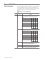
Manual Organization
This manual is divided into eight chapters. The following chart
shows each chapter with its corresponding title and a brief overview
of the topics covered in that chapter.
Chapter
Title
Topics Covered
3#/3'#4 ,$ 1&# +-21 ,"2)#
#0!/'-1',+ ,$ 1&# *,"2)# '+!)2"'+% %#+#/) +" &/"4/#
$#12/#0
+01))'+% 1&# +-21 ,"2)#
,"2)# -,4#/ /#.2'/#*#+10 (#6'+% !&00'0 ),!1',+
'/'+% ,$ $'#)" 4'/'+% /*
,"2)# /,%/**'+%
,4 1, -/,%/* 6,2/ -/,%/** )# !,+1/,))#/ $,/ 1&'0 *,"2)#
*-)# -/,%/*0
,"2)# ,+$'%2/1',+
/"4/# +" 0,$14/# !,+$'%2/1',+
,"2)# 4/'1# ),!( $,/*1
,"2)# 1120 +" +-21 1
#"'+% "1 $/,* 6,2/ *,"2)#
,"2)# /#" ),!( $,/*1
,"2)# )' /1',+
,4 1, !)' /1# 6,2/ *,"2)#
/,2 )#0&,,1'+%
'%+,01'!0 /#-,/1#" 6 1&# *,"2)#
--#+"'5 -#!'$'!1',+0
,2/ *,"2)#0 0-#!'$'!1',+0
--#+"'5 /,%/**'+% 5*-)#0
--#+"'5 1 ,/*10
+$,/*1',+ ,+ 0'%+#" *%+'12"# '+/6 +" 0
!,*-)#*#+1 '+/6
2 )'!1',+ 6 P–2
Using This Manual
Chapter
Title
Topics Covered
Appendix D
Block Transfer with Mini-PLC-2 and
Mini-PLC-2/20
How to use GET-GET instructions for block transfer with
Mini-PLC-2 and Mini-PLC-2/20 processors
Appendix E
Differences between Series A, B, C and
D versions
Lists differences from Series A 1771-IXE module
Appendix F
Thermocouple Characteristics
Extractions from NBS Monograph 125 (IPTS-68)
Warnings and Cautions
This manual contains warnings and cautions.
!
!
ATTENTION: A warning indicates where you may
be injured if you use your equipment improperly.
ATTENTION: Cautions indicate where equipment
may be damaged from misuse.
You should read and understand cautions and warnings before
performing the procedures they precede.
Related Products
You can install your input module in any system that uses
Allen–Bradley programmable controllers with block transfer
capability and the 1771 I/O structure.
Contact your nearest Allen–Bradley office for more information
about your programmable controllers.
Product Compatibility
Publication 1771-6.5.130 - May 1999
These input modules can be used with any 1771 I/O chassis.
Communication between the analog module and the processor is
bidirectional. The processor block–transfers output data through the
output image table to the module and block–transfers input data from
the module through the input image table. The module also requires
an area in the data table to store the read block and write block data.
I/O image table use is an important factor in module placement and
addressing selection. The module’s data table use is listed in the
following table.
Using This Manual
P–3
Table P.A Compatibility and Use of Data Table
Catalog
Number
+-10
* %$
'0/
Use of Data Table
10-10 $ #
* %$ ),"(
'0/
,.#/
.'0$
),"(
,.#/
Compatibility
/),0
$/
##.$//'+%
& //'/
/),0
/),0 $.'$/
$/
$/
+# ,*- 0'!)$ 2'0& "& //'/
,*- 0'!)$ 2'0& "& //'/
$/ ,*- 0'!)$ 2'0&,10 .$/0.'"0',+
, $/0.'"0$# 0, ",*-)$*$+0 .3 *,#1)$ -) "$*$+0
You can place your input module in any I/O module slot of the I/O
chassis. You can put:
• two input modules in the same module group
• an input and an output module in the same module group.
Do not put the module in the same module group as a discrete high
density module unless you are using 1 or 1/2 slot addressing. Avoid
placing this module close to AC modules or high voltage DC
modules.
Related Publications
For a list of publications with information on Allen–Bradley
programmable controller products, consult our publication index
SD499.
1!)'" 0',+ 3 P–4
Using This Manual
Table of Contents
Overview of the
Thermocouple/Millivolt Input
Module
Chapter 1
Installing the
Thermocouple/Millivolt Input
Module
Chapter 2
Module Programming
Chapter 3
*#26'4 $,'%6+8'5 1&7.' '5%4+26+10 '#674'5 1( 6*' 0276 1&7.' 19 0#.1) 1&7.'5 1//70+%#6' 9+6* 41)4#//#$.' 10641..'45
%%74#%; '66+0) 6#46'& *#26'4 7//#4; *#26'4 $,'%6+8'5 '(14' "17 056#.. "174 0276 1&7.' 4'8'06 .'%64156#6+% +5%*#4)' 0&'456#0& 1/2.+#0%' 61 7412'#0 0+10 +4'%6+8'5 +4'%6+8' 19 1.6#)' +4'%6+8' 0&'456#0& 41&7%6 1/2#6+$+.+6; #.%7.#6' 19'4 '37+4'/'065 '6'4/+0' 1&7.' .#%'/'06 +0 6*' *#55+5 '; 6*' #%-2.#0' 100'%614 056#.. 6*' 1&7.' #0& +'.& !+4+0) 4/ 100'%6 !+4+0) 61 6*' +'.& !+4+0) 4/ #$.' '0)6*5 4170&+0) 06'424'6 6#675 0&+%#6145 *#26'4 7//#4; *#26'4 $,'%6+8'5 .1%- 4#05('4 41)4#//+0) < 41)4#//+0) :#/2.' 41)4#/ %6+10 < 41)4#//+0) :#/2.' 41)4#/ %6+10 <
41)4#//+0) :#/2.' 1&7.' %#0 +/' *#26'4 7//#4; 7$.+%#6+10 <
< #; toc-ii
Table of Contents
Module Configuration
Chapter 4
+$37(5 %-(&7,9(6 21),*85,1* 7+( +(502&283/(,//,92/7 1387 2'8/( " 1387 ;3( (03(5$785( &$/( $7$ 250$7 ($/ ,0( $03/,1* +$11(/ /$506 $/,%5$7,21 21),*85$7,21 /2&. )25 $ /2&. 5$16)(5 !5,7( ,7!25' (6&5,37,216 +$37(5 800$5; Module Status and Input
Data
Chapter 5
Module Calibration
Chapter 6
+$37(5 %-(&7,9(6 ($',1* $7$ )520 7+( 2'8/( ,7!25' (6&5,37,216 +$37(5 800$5; +$37(5 %-(&7,9( 22/6 $1' 48,30(17 $/,%5$7,1* #285 1387 2'8/( %287 872<$/,%5$7,21 (5)250,1* 872<$/,%5$7,21 ))6(7 $/,%5$7,21 $,1 $/,%5$7,21 $9( $/,%5$7,21 $/8(6 (5)250,1* $18$/ $/,%5$7,21 (77,1* +$11(/ ))6(7 $/,%5$7,21 (77,1* +$11(/ $,1 $/,%5$7,21 +$37(5 800$5; Troubleshooting
Appendix A
+(502&283/(,//,92/7 1387 2'8/( &&85$&; ($' (6,67$1&( 203(16$7,21 285&( 03('$1&( 203(16$7,21 )25 ,//,92/7 13876 ,/7(5,1* 8%/,&$7,21 <
< $; Chapter 7
+$37(5 %-(&7,9( ,$*1267,&6 (3257(' %; 7+( 2'8/( 528%/(6+227,1* :,7+ 7+( 1',&$7256 7$786 (3257(' %; 7+( 2'8/( +$37(5 800$5; Specifications
Table of Contents
Programming Examples
Appendix B
Sample Programs for the Input Module . . . . . . . . . . . . . . . . . . . . .
PLC-2 Family Processors . . . . . . . . . . . . . . . . . . . . . . . . . . . . . .
PLC-3 Family Processors . . . . . . . . . . . . . . . . . . . . . . . . . . . . . .
PLC-5 Family Processors . . . . . . . . . . . . . . . . . . . . . . . . . . . . . .
Data Table Formats
toc-iii
B-1
B-1
B-2
B-3
Appendix C
4-Digit Binary Coded Decimal (BCD) . . . . . . . . . . . . . . . . . . . . . .
Signed-magnitude Binary . . . . . . . . . . . . . . . . . . . . . . . . . . . . . . .
Two's Complement Binary . . . . . . . . . . . . . . . . . . . . . . . . . . . . . .
Block Transfer (Mini-PLC-2
and PLC-2/20 Processors)
Appendix D
Differences Between Series
A, Series B, Series C and
Series D
Thermocouple/Millivolt
Input Modules
Appendix E
Thermocouple Restrictions
(Extracted from NBS
Monograph 125 (IPTS-68))
Appendix F
Multiple GET Instructions - Mini-PLC-2 and PLC-2/20 Processors .
Setting the Block Length (Multiple GET Instructions only) . . . . . . . .
Major Differences between Series . . . . . . . . . . . . . . . . . . . . . . . . .
C-1
C-2
C-2
D-1
D-2
E-1
General . . . . . . . . . . . . . . . . . . . . . . . . . . . . . . . . . . . . . . . . . . .
F-1
J (Iron vs Copper-Nickel <Constantan*>) Type Thermocouple . . .
F-1
K (Nickel-Chromium vs Nickel-Aluminum) Type Thermocouple . .
F-2
T (Copper vs Copper-Nickel <Constantan*>) Type Thermocouple
F-3
E (Nickel-Chromium vs Copper-Nickel <Constantan*>) Type
Thermocouple . . . . . . . . . . . . . . . . . . . . . . . . . . . . . . . . . .
F-4
S (Platinum-10% Rhodium vs Platinum) & R (Platinum-13% Rhodium vs
Platinum) Type Thermocouples . . . . . . . . . . . . . . . . . . . . . .
F-5
Publication 1771Ć6.5.130 Ć May 1999
Table of Contents
Chapter
1
Overview of the
Thermocouple/Millivolt Input
Module
Chapter Objectives
This chapter gives you information on:
• features of the input module
• how an input module communicates with programmable
controllers
Module Description
The Thermocouple/Millivolt input module is an intelligent block
transfer module that interfaces analog input signals with any
Allen–Bradley programmable controllers that have block transfer
capability. Block transfer programming moves input data words from
the module’s memory to a designated area in the processor data table
in a single scan. It also moves configuration words from the
processor data table to module memory.
The input module is a single slot module which does not require an
external power supply. After scanning the analog inputs, the input
data is converted to a specified data type in a digital format to be
transferred to the processor’s data table on request. The block
transfer mode is disabled until this input scan is complete.
Consequently, the minimum interval between block transfer reads is
the same as the total input update time for each analog input
module (50ms).
Features of the Input
Module
The 1771–IXE/D module senses up to 8 differential analog inputs
and converts them to values compatible with Allen–Bradley
programmable controllers.
This module’s features include:
• 8 input channels configurable for thermocouple input ranges or
•
•
•
•
•
millivolt input ranges: Types E, J, K, T, R and S thermocouples
and +100 millivolts
two types of inputs allowed: 4 of one input type and 4 of another
cold junction compensation
scaling to selected temperature range in oC or oF
temperature resolution of 1oC or 1oF, millivolt resolution to 10
microvolts
user selectable high and low temperature alarms
1–2
Overview of the Thermocouple/Millivolt Input Module
•
•
•
•
•
How Analog Modules
Communicate with
Programmable Controllers
all features selectable through programming
self–diagnostics and status reporting at power–up
detection of open circuit if thermocouple fails
automatic offset and gain calibration for each channel
software calibration of all channels, eliminating potentiometers
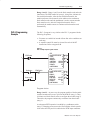
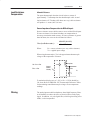
The processor transfers data to and from the module using BTW
(block transfer write) and BTR (block transfer read) instructions in
your ladder diagram program. These instructions let the processor
obtain input values and status from the module, and let you establish
the module’s mode of operation (Figure 1.1).
1. The processor transfers your configuration data and calibration
values to the module using a block transfer write instruction.
2. External devices generate analog signals that are transmitted to
the module.
Figure 1.1
Communication Between Processor and Module
#(*,2
-#, ,*$,(
* /.+/. #0&!#-
%#,(*!*/+'#&''&0*'.
)+/. *"/'#
,*!#--*,
%*1)
/ '&!.&*) 3
3 2 Overview of the Thermocouple/Millivolt Input Module
1–3
3. The module converts analog signals into binary or BCD format,
and stores theses values until the processor requests their
transfer.
4. When instructed by your ladder program, the processor performs
a read block transfer of the values and stores them in a data table.
5. The processor and module determine that the transfer was made
without error, and that input values are within specified range.
6. Your ladder program can use and/or move the data (if valid)
before it is written over by the transfer of new data in a
subsequent transfer.
7. Your ladder program should allow write block transfers to the
module only when enabled by the operator at power–up.
Accuracy
The accuracy of the input module is described in Appendix A.
Getting Started
Your input module package contains the following items. Please
check that each part is included and correct before proceeding.
&"$$(%!
!! )$!'
#%(' $(!
' $
Input Module
Field Wiring Arm
' $ User’s Manual
User's Manual
Chapter Summary
In this chapter you read about the functional aspects of the input
module and how the module communicates with programmable
controllers.
(! ' $# +
+ * 1–4
Overview of the Thermocouple/Millivolt Input Module
Chapter
2
Installing the
Thermocouple/Millivolt Input
Module
Chapter Objectives
This chapter gives you information on:
•
•
•
•
•
Before You Install Your
Input Module
calculating the chassis power requirement
choosing the module’s location in the I/O chassis
keying a chassis slot for your module
wiring the input module’s field wiring arm
installing the input module
Before installing your input module in the I/O chassis you must:
Action required:
Prevent Electrostatic
Discharge
Refer to:
) ( ( $#*& &%)&!"(' # !#) ' " '''
) ( #*& %)&!"('
(&!" *& (# $ ( !#) " ( '''
#) #(#" " ( '''
+ ( $ " #""(#& " ( '''
#) +"
#""(#"' (# ( *&" &!
#""(" &" " &#)""
The thermocouple/mV input module is sensitive to electrostatic
discharge.
!
ATTENTION: Electrostatic discharge can damage
integrated circuits or semiconductors if you touch
backplane connector pins. Follow these guidelines
when you handle the module:
• Touch a grounded object to discharge static potential
• Wear an approved wrist-strap grounding device
• Do not touch the backplane connector or
connector pins
• Do not touch circuit components inside the module
• If available, use a static-safe work station
• When not in use, keep the module in its
static-shield bag
) (#" , , + 2–2
Installing the Thermocouple/Millivolt Input Module
Understand Compliance to
European Union Directives
If this product has the CE mark it is approved for installation within
the European Union and EEA regions. It has been designed and
tested to meet the following directives.
EMC Directive
This product is tested to meet Council Directive 89/336/EEC
Electromagnetic Compatibility (EMC) and the following standards,
in whole or in part, documented in a technical construction file:
• EN 50081-2EMC – Generic Emission Standard,
Part 2 – Industrial Environment
• EN 50082-2EMC – Generic Immunity Standard,
Part 2 – Industrial Environment
This product is intended for use in an industrial environment.
Low Voltage Directive
This product is tested to meet Council Directive 73/23/EEC
Low Voltage, by applying the safety requirements of EN 61131–2
Programmable Controllers, Part 2 – Equipment Requirements and
Tests.
For specific information required by EN 61131-2, see the appropriate
sections in this publication, as well as Allen-Bradley publication
1770-4.1, Industrial Automation Wiring and Grounding Guidelines.
Open style devices must be provided with environmental and safety
protection by proper mounting in enclosures designed for specific
application conditions. See NEMA Standards publication 250 and
IEC publication 529, as applicable, for explanations of the degrees of
protection provided by different types of enclosure.
Understand Product
Compatibility
The 1771-IXE module can be used with any 1771 I/O chassis.
Compatibility and data table use is listed below.
1% .& !2! !"+%
!2!+.'
3,"%0
6
.,/!2)")+)25
-/32
,!'%
)21
32/32
,!'%
)21
%!$
+.#*
.0$1
0)2%
+.#*
.0$1
$$0%11)-'
6+.2
6+.2
6+.2
(!11)1
)
%0)%1
.,/!2)"+% 4)2( 6 6 6
.,/!2)"+% 4)2( 6 6 6 6 6
.,/!2)"+% 4)2(.32 0%120)#2).-
Do not use this module with cat. no. 1771-AL PLC-2/20 or 2/30
Local Adapter.
3"+)#!2).- 6
6 !5 Installing the Thermocouple/Millivolt Input Module
Calculate Power
Requirements
2–3
The module receives its power through the 1771 I/O power supply
and requires 850mA from the backplane.
Add this current to the requirements of all other modules in the I/O
chassis to prevent overloading the chassis backplane and/or
backplane power supply.
!
Determine Module
Placement in the I/O
Chassis
ATTENTION: Do not insert or remove modules from
the I/O chassis while system power is ON. Failure to
observe this rule could result in damage to module
circuitry.
Place your module in any I/O module slot of the I/O chassis except
for the extreme left slot. This slot is reserved for PC processors or
adapter modules.
Group your modules to minimize adverse affects from radiated
electrical noise and heat. We recommend the following.
• Group analog input and low voltage dc modules away from ac
modules or high voltage dc modules to minimize electrical noise
interference.
• Do not place this module in the same I/O group with a discrete
high-density I/O module when using 2-slot addressing. This
module uses a byte in both the input and output image tables for
block transfer.
Key the Backplane Connector
Place your module in any slot in the chassis
except the leftmost slot which is reserved for
processors or adapters.
!%&! & ) % & " ! &!$% &! !$$%"! &!
& ) %!&% ! & !'
& ) %
&( 20 22
&( 24 26
ATTENTION: Observe the
following precautions when
inserting or removing keys:
!
• insert or remove keys with
your fingers
• make sure that key placement
is correct
Incorrect keying or the use of a tool
can result in damage to the
backplane connector and possible
system faults.
%%%
""$ ! &!$
*
!' & "!%&! ! &%
% %'%#' & %)%& % $($ % %$&! ! $ & &)"
! !' %%$)
'&! * * ) 2–4
Installing the Thermocouple/Millivolt Input Module
Install the Module and Field
Wiring Arm
!
ATTENTION: Remove power from the 1771 I/O
chassis backplane and field wiring arm before
removing or installing an I/O module.
• Failure to remove power from the backplane or wiring arm could cause module damage, degradation of
performance, or injury.
• Failure to remove power from the backplane could
cause injury or equipment damage due to possible
unexpected operation.
1
1 1 1
1
1 !**"*
1 1 1
1 )"* !**"*
$'#"& +
$'#"& )
$'#"& ) ("&
) ,"*
) ,"*
',$
&( +! !**"* $+! '-)
+! +'( ' +! %',$ +' *,) "+
2
',$
."& +! !**"* $'#"& ) '.& "&+' ($ +' *,)
+! %',$* # *,) +! $'#"& ("&* & .")"& )%
++! +! .")"& )% 1 +' +! !')"0'&+$
) + +! '++'% ' +! !**"*
! .")"& )% ("-'+* ,(.) & '&&+* ."+!
+! %',$ *' /', & "&*+$$ ') )%'- +!
%',$ ."+!',+ "*'&&+"& +! .")*
1
)%'-
!')"0'&+$ )
,$"+"'& 1
1 / install
Installing the Thermocouple/Millivolt Input Module
Connect Wiring to the
Field Wiring Arm
2–5
Connect your I/O devices to the cat. no. 1771-WI wiring arm
shipped with the module.
!
ATTENTION: Remove power from the 1771 I/O
chassis backplane and field wiring arm before
removing or installing an I/O module.
• Failure to remove power from the backplane or
wiring arm could cause module damage, degradation
of performance, or injury.
• Failure to remove power from the backplane could
cause injury or equipment damage due to possible
unexpected operation.
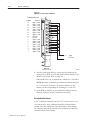
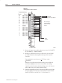
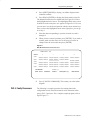
Input connections for the 1771-IXE/D are shown below.
Figure 2.1
Wiring Connections for the 1771-IXE Series D
Terminal Identification
Channel 1
–
+
–
Channel 2
1
1
2
Wiring Arm
Cat. No. 1771-WI
+
Do not use
3
4
5
6
7
8
Input 1 (+ lead)
Input 1 (- lead)
Input 2 (+ lead)
Input 2 (- lead)
Input 3 (+ lead)
Input 3 (- lead)
Input 4 (+ lead)
Input 4 (- lead)
Not Used
Not used
Input 5 (+ lead)
Input 5 (- lead)
Input 6 (+ lead)
Input 6 (- lead)
Input 7 (+ lead)
Input 7 (- lead)
Input 8 (+ lead)
Input 8 (- lead)
9
10
11
12
18
17
16
15
14
13
12
11
10
9
8
7
6
5
4
3
2
1
Function
13
14
15
16
17
18
Terminal
Short circuit
unused pins
Connect positive thermocouple leads
to even-numbered terminals, negative
leads to odd-numbered terminals.
Ground cable shield to I/O chassis
mounting bolt.
The sensor cable must be shielded. The shield must:
• extend the length of the cable, but be connected only at the 1771 I/O chassis
• extend up to the point of termination
Important:
The shield should extend to the termination point, exposing just enough cable to
adequately terminate the inner conductors. Use heat shrink or another suitable
insulation where the wire exits the cable jacket.
10527-I
Publication 1771Ć6.5.130 Ć May 1999
2–6
Installing the Thermocouple/Millivolt Input Module
Cable Lengths
Recommended maximum cable length for voltage-mode input
devices is 50 feet, due to possible signal degradation and electrical
noise immunity in typical industrial environments.
Grounding
1
When using shielded cable wire, ground the foil shield and drain
wire only at one end of the cable. We recommend that you wrap the
foil shield and drain wire together, and connect them to a chassis
mounting bolt, grounding stud or chassis single-point grounding
point. Use heat shrink tubing to seal the exit point of the wires. At
the opposite end of the cable, tape exposed shield and drain wire
with electrical tape to insulate it from electrical contact.
"#-& 306/%*/(
&.07& " -&/(5) 0' $"#-&
+"$,&5 '30. 5)& &-%&/ $"#-&
6-- 5)& '0*- 4)*&-% "/% #"3&
%3"*/ 8*3& '30. 5)& */46-"5&%
8*3&4 "3& %3"*/
8*3&
&-%&/ "#-&
8*45 5)& '0*- 4)*&-% "/% %3"*/
8*3& 50(&5)&3 50 '03. " 4*/(-&
453"/%
55"$) " (306/% -6( "/% "11-:
)&"5 4)3*/, 56#*/( 50 5)& &9*5 "3&"
&/(5) "4 /&&%&%
/46-"5&%
8*3&4
0*4)*&-%
2
)"44*4 306/%
!)&/ :06 $0//&$5 (306/%*/( $0/%6$5034 50 5)& $)"44*4
(306/%*/( 456% 1-"$& " 45"3 8"4)&3 6/%&3 5)& '*345 -6( 5)&/
1-"$& " /65 8*5) $"15*7& -0$, 8"4)&3 0/ 501 0' &"$) (306/% -6(
SingleĆpoint Grounding
95&/% 4)*&-% 50 5&3.*/"5*0/ 10*/5 9104& +645 &/06() $"#-& 50
"%&26"5&-: 5&3.*/"5& *//&3 $0/%6$5034
306/% 6(
65
65 "/% "15*7&
!"4)&3
306/%*/( 56%
)"44*4
*%& -"5&
5"3
!"4)&3
306/% 6(
4& )&"5 4)3*/, 56#*/( 03
05)&3 46*5"#-& */46-"5*0/
8)&3& 8*3& &9*54 $"#-&
+"$,&5
)*&-% "/% 3"*/
58*45&% 50(&5)&3
)*&-% "/% 3"*/
58*45&% 50(&5)&3
4& 5)& $61 8"4)&3 *' $3*.1;0/ -6(4 "3& /05 64&%
)3&"%;'03.*/( 4$3&8
95&3/"-;5005) !"4)&34
&'&3 50 /%6453*"- 650."5*0/ !*3*/( "/% 306/%*/( 6*%&-*/&4 16#-*$"5*0/ ;
'03 "%%*5*0/"- */'03."5*0/
6#-*$"5*0/ ; ; ": Installing the Thermocouple/Millivolt Input Module
Interpret Status Indicators
!
!
Chapter Summary
2–7
The front panel of the thermocouple/mV input module contains a
green RUN indicator and a red FAULT indicator. At power-up, the
module momentarily turns on the red indicator as a lamp test, then
checks for:
• correct RAM operation
• EPROM operation
• EEPROM operation
• a valid write block transfer with configuration data
If there is no fault, the red indicator turns off.
Thereafter, the module lights the green RUN indicator when
operating without fault, or lights the red FAULT indicator when it
detects fault conditions. If the red FAULT indicator is on, block
transfers will be inhibited. Possible module fault causes and
corrective action are discussed in Chapter 8, Troubleshooting.
In this chapter you learned how to install your input module in an
existing programmable controller system and how to wire to the field
wiring arm.
"! $ $ # 2–8
Installing the Thermocouple/Millivolt Input Module
Chapter
3
Chapter Objectives
In this chapter, we describe
• Block Transfer programming
• Sample programs in the PLC–2, PLC–3 and PLC–5 processors
• Module scan time issues
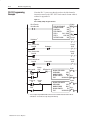
Block Transfer
Programming
Your module communicates with the processor through bidirectional
block transfers. This is the sequential operation of both read and
write block transfer instructions.
The block transfer write (BTW) instruction is initiated when the
analog module is first powered up, and subsequently only when the
programmer wants to write a new configuration to the module. At all
other times the module is basically in a repetitive block transfer read
(BTR) mode.
The following example programs accomplish this handshaking
routine. These are minimum programs; all rungs and conditioning
must be included in your application program. You can disable
BTRs, or add interlocks to prevent writes if desired. Do not eliminate
any storage bits or interlocks included in the sample programs. If
interlocks are removed, the program may not work properly.
Your analog input module will work with a default configuration of
all zeroes entered in the configuration block. See the configuration
default section to understand what this configuration looks like.
Also, refer to Appendix B for example configuration blocks and
instruction addresses to get started.
Your program should monitor status bits (such as overrange,
underrange, alarms, etc.) and block transfer read activity.
The following example programs illustrate the minimum
programming required for communication to take place.
3–2
Module Programming
PLCĆ2 Programming
Example
Note that PLC–2 processors that do not have the block transfer
instruction must use the GET–GET block transfer format which is
outlined in Appendix D.
Figure 3.1
PLC-2 Family Sample Program Structure
86-'87732 03(/ 5&26+*5#5.7*
32* .7
735&,*
.7 735&,*
.7 39*584.7
!
39*584.7
735&,*
.7 735&,*
.7 735&,*
.7 !
86-'87732
03(/ 5&26+*5#5.7*
32* .7
03(/ 5&26+*5*&)
32* .7
2&'0*
"
! $$$
$$$
$$$ 32*
%%%%$$$$ $$$$$$
$$$ 735&,*
.7 03(/ 5&26+*5
*&)32*.7
39*584
.7
735&,*
.7 735&,*
.7 32*.7
$
$$$
!
$$
$$$$$$$$
$# $$$
!
$$
$$$$$$$$
2&'0*
$
32*
2&'0*
$
32*
$
%38 (&2 5*40&(* 7-* 486-'87732 9.7- & 7.1*5 )32* '.7 73 .2.7.&7* 7-* '03(/ 75&26+*5 95.7* 32
& 7.1*) '&6.6 %38 (&2 &063 86* &2: 6735&,* '.7 .2 1*135:
8'0.(&7.32 ;
; &: $
Module Programming
3–3
Program Action
Rung 1 – Block transfer read buffer: the file–to–file move
instruction holds the block transfer read (BTR) data (file A) until the
processor checks the data integrity.
1. If the data was successfully transferred, the processor energizes
the BTR done bit, initiating a data transfer to the buffer (file R)
for use in the program.
2. If the data is corrupted during the BTR operation, the BTR done
bit is not energized and data is not transferred to the buffer file. In
this case, the data in the BTR file will be overwritten by data
from the next BTR.
Rungs 2 and 3 – These rungs provide for a user–initiated block
transfer write (BTW) after the module is initialized at power–up.
Pressing the pushbutton locks out BTR operation and initiates a
BTW that configures the module. Block transfer writes will continue
for as long as the pushbutton remains closed.
Rungs 4 and 5 – These rungs provide a ”read–write–read” sequence
to the module at power–up. They also ensure that only one block
transfer (read or write) is enabled during a particular program scan.
Rungs 6 and 7 – These rungs are the conditioning block transfer
rungs. Include all the input conditioning shown in the example
program.
3–4
Module Programming
PLCĆ3 Programming
Example
Block transfer instructions with the PLC–3 processor use one binary
file in a data table section for module location and other related data.
This is the block transfer control file. The block transfer data file
stores data that you want transferred to the module (when
programming a block transfer write) or from the module (when
programming a block transfer read). The address of the block
transfer data files are stored in the block transfer control file.
The industrial terminal prompts you to create a control file when a
block transfer instruction is being programmed. The same block
transfer control file is used for both the read and write
instructions for your module. A different block transfer control file
is required for every module.
A sample program segment with block transfer instructions is shown
in Figure 3.2, and described below.
Figure 3.2
PLC-3 Family Sample Program Structure
!
!!!
!
!!!!!
!!!!!!!!
!
!!!!!!!!
+-$* /",0'&/
&"% -,& )1
20(#211-,
+-$* /",0'&/
/)1& -,& )1
-3&/2.
)1
,"#+&
-,&
//-/
,"#+&
! !!!
-,&
!
!!!!!
!!!!!!!!
//-/
!
!!!!!!!!
Program Action
At power–up, the user program examines the BTR done bit in the
block transfer read file, initiates a write block transfer to configure
the module, and then does consecutive read block transfers
continuously. The power–up bit can be examined and used anywhere
in the program.
2#+)$"1)-, 5 5 "4 Module Programming
3–5
Rungs 1 and 2 – Rungs 1 and 2 are the block transfer read and write
instructions. The BTR enable bit in rung 1, being false, initiates the
first read block transfer. After the first read block transfer, the
module performs a block transfer write and then does continuous
block transfer reads until the pushbutton is used to request another
block transfer write. After this single block transfer write is
performed, the module returns to continuous block transfer reads
automatically.
PLCĆ5 Programming
Example
The PLC–5 program is very similar to the PLC–3 program with the
following exceptions:
• You must use enable bits instead of done bits as the conditions on
each rung.
• A separate control file must be selected for each of the BT
instructions. Refer to Appendix B.
Figure 3.3
PLC-5 Family Sample Program Structure
!
!
!
!
!!!!!
!!!!!
!!
)"#(%
/-&#/..*)
)"#(%
*0%,/+'.
! !
!
!
!!!!!
!!!!!
!!
Program Action
Rungs 1 and 2 – At power–up, the program enables a block transfer
read and examines the power–up bit in the BTR file (rung 1). Then,
it initiates one block transfer write to configure the module (rung 2).
Thereafter, the program continuously reads data from the module
(rung 1).
A subsequent BTW operation is enabled by a pushbutton switch
(rung 2). Changing processor mode will not initiate a block transfer
write unless the first pass bit is added to the BTW input conditions.
/#('$".'*) 2 2 "1 3–6
Module Programming
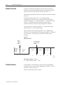
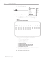
Module Scan Time
Scan time is defined as the amount of time it takes for the input
module to read the input channels and place new data into the data
buffer. Scan time for your module is shown in Figure 3.4.
The following description references the sequence numbers in Figure
Figure 3.4.
Following a block transfer write “1” the module inhibits
communication until after it has configured the data and loaded
calibration constants “2”, scanned the inputs “3”, and filled the data
buffer “4”. Write block transfers, therefore, should only be
performed when the module is being configured or calibrated.
Any time after the second scan begins “5”, a block transfer read
(BTR) request “6” can be acknowledged.
When operated in the default mode (RTS) = 00, a BTR will be
released every 50 milliseconds. When operated in RTS = T, BTR will
be waived until ”T”millseconds, at which time 1 BTR will be
released.
Figure 3.4
Block Transfer Time
" #
#
%"&%
%'
#
%"&%
%'
!
#( ) '# $%#%! #
'%"&%
#"(%
!
&' "
" "
% "
Internal Scan time = 50msec
T = 100ms, 200ms, 300ms ... 3.1sec.
Chapter Summary
In this chapter, you learned how to program your programmable
controller. You were given sample programs for your PLC–2, PLC–3
and PLC–5 family processors.
You also read about module scan time.
( '#" +
+ * Chapter
4
Module Configuration
Chapter Objectives
Configuring the
Thermocouple/Millivolt
Input Module (1771-IXE/D)
In this chapter you will read how to configure your module’s
hardware, condition your inputs and enter your data.
Because of the many analog devices available and the wide variety
of possible configurations, you must configure your module to
conform to the analog device and specific application that you have
chosen. Data is conditioned through a group of data table words that
are transferred to the module using a block transfer write instruction.
You can configure the following features for the 1771–IXE/D
module:
•
•
•
•
•
•
•
type of input
one or two input types
oC or oF
data format
real time sampling
alarming
calibration
Configure your module for its intended operation by means of your
programming terminal and write block transfers.
Note: Programmable controllers that use 6200 software
programming tools can take advantage of the IOCONFIG utility to
configure this module. IOCONFIG uses menu–based screens for
configuration without having to set individual bits in particular
locations. Refer to your 6200 software literature for details.
During normal operation, the processor transfers from 1 to 27 words
to the module when you program a BTW instruction to the module’s
address. The BTW file contains configuration words, high and low
channel alarm settings, and calibration values that you enter for each
channel. When a block transfer length of 0 is programmed, the
1771–IXE/D will respond with the Series A default value of 27.
4–2
Module Configuration
Input Type
The thermocouple/millivolt input module accepts the following types
of inputs:
Table 4.A
Types of Inputs
Input Type
Input Type
Temperature
Range oC
00
Bits
01
02
03
Bits
04
05
#$$#-'$+
#$$#-'$+
+' " )%'',($
+' +' +' +' +' +' The input type is selected by setting bits in the block transfer write
(BTW) file. Two different inputs can be selected. You can have 4
inputs set for one type, and 4 inputs set for another type; or you can
have all inputs the same. If you select different types of inputs, set bit
06 to 1. If you do not select 2 different input types, the module
defaults to all inputs set to those selected by bits 00 –02.
+ +" * #+*
!') #&(,+ +.( + +"#* #+ !') #!! ) &+
#&(,+ +.( * * +$ Word
17
Temperature Scale
16
15
14
%($ #%
13
12
11
')%+
10
07
06
05
04
&(,+ .(
03
02
01
&(,+ .(
The temperature scale reported by the module is selected by setting
bit 10 in the configuration word. When bit 10 is set (1), the
temperature is reported in degrees Fahrenheit. When reset (0), the
temperature is reported in degrees Celsius.
The temperature bit 10 is ignored when the millivolt input type is
selected.
,$#+#'& /
/ . 00
Module Configuration
Data Format
4–3
You must indicate what format will be used to read data from your
module. Typically, BCD is selected with PLC–2 processors, and
binary (also referred to as integer or decimal) is selected with PLC–3
and PLC–5 processors. See Table 4.B and Appendix C for details on
Data Format.
Table 4.B Selecting Format for Reading Data
Decimal Bit 10
Octal Bit 12
Real Time Sampling
Decimal Bit 9
Octal Bit 11
Data Format
# ! #
!" #
!" #
The real time sampling (RTS) mode of operation provides data from
a fixed time period for use by the processor. RTS is invaluable for
time based functions (such as PID and totalization) in the PLC. It
allows accurate time based calculations in local or remote I/O racks.
In the RTS mode the module scans and updates its inputs at a user
defined time interval ( ∆T) instead of the default interval. The
module ignores block transfer read (BTR) requests for data until the
sample time period elapses. The BTR of a particular data set
occurs only once at the end of the sample period and subsequent
requests for transferred data are ignored by the module until a new
data set is available. If a BTR does not occur before the end of the
next RTS period, a time–out bit is set in the BTR status area. When
set, this bit indicates that at least one data set was not transferred to
the processor. (The actual number of data sets missed is unknown.)
The time–out bit is reset at the completion of the BTR.
Set appropriate bits in the BTW data file to enable the RTS mode.
You can select RTS periods ranging from 100 milliseconds (msec) to
3.1 seconds in increments of 100msec. Refer to Table 4.C below for
actual bit settings. Note that the default mode of operation is
implemented by placing all zeroes in bits 13 through 17. Note that
binary representation of the RTS bit string is the RTS period X
100msec. For example, 900msec = 01001 = (9 X 100msec).
"! $
$ # 4–4
Module Configuration
Table 4.C
Bit Settings for the Real Time Sample Mode
Decimal Bits
Octal Bits
15
17
14
16
13
15
12
14
11
13
Sample Time Period
! Important: Use decimally addressed bit locations for PLC–5
processors.
Channel Alarms
Calibration
! #
# " Each channel has an alarm enable bit, an alarm polarity bit, and high
and low alarm values associated with it. These bits and words are
explained in the bit/word definitions in Table 4.E.
You have the ability to calibrate this module using auto–calibration
or by manually setting the individual channel words. Words 20
through 27 in the configuration word (Table 4.E) are the calibration
words for channels 1 through 8 respectively. Calibration is explained
in chapter 6.
Module Configuration
Configuration Block for a
Block Transfer Write
4–5
The complete configuration block for the block transfer write to the
module is defined in Table 4.D below.
Table 4.D
Configuration Block for Thermocouple/Millivolt Input
Module Block Transfer Write
Word
17
16
15
14
13
12
),(# ')#
11
10
07
+.)0
+0 /#"
'%& (.)/ +(.'03 +*# '0 ,#. '*,10 !&**#(
&**#( +2 (.) (1#
&**#( '%& (.) (1#
&**#( +2 (.) (1#
&**#( '%& (.) (1#
&**#( +2 (.) (1#
&**#( '%& (.) (1#
&**#( +2 (.) (1#
&**#( '%& (.) (1#
&**#( +2 (.) (1#
&**#( '%& (.) (1#
&**#( +2 (.) (1#
&**#( '%& (.) (1#
&**#( +2 (.) (1#
&**#( '%& (.) (1#
&**#( +2 (.) (1#
&**#( '%& (.) (1#
(' .0'+* (1#/ $+. &**#( (' .0'+* (1#/ $+. &**#( (' .0'+* (1#/ $+. &**#( (' .0'+* (1#/ $+. &**#( (' .0'+* (1#/ $+. &**#( (' .0'+* (1#/ $+. &**#( (' .0'+* (1#/ $+. &**#( (' .0'+* (1#/ $+. &**#( 10+!(' .0'+* #-1#/0 +."
06
05
04
03
02
3,#
01
3,#
* (# &**#( (.)/ +*# '0 ,#. '*,10 !&**#(
+2 (.)/ +(.'03 +*# '0 ,#. '*,10 !&**#(
E = enable bit for input types (refer to bit/word description)
T = temperature scale bit (refer to bit/word description)
1 ('!0'+* 4 4 3 00
4–6
Module Configuration
Bit/Word Descriptions
Bit/word descriptions of BTW file words 1 thru 3 (configuration), 4
thru 19 (channel alarm values), and 20 thru 27 (calibration values)
are presented in Table 4.E. Enter data into the BTW instruction after
entering the instruction into your ladder diagram program.
Table 4.E
Bit/Word Definitions for Thermocouple/Millivolt Input
Module
Word
Bits
,.# !(0/ Description
+-10 04-$ ",#$/ %,. (+-10/ 0'.1 ,. 0'.1 (% !(0 (/ /$0 0, $))/ 0'$ *,#1)$ 3' 0 04-$ ,% (+-10 #$2("$ 4,1 ",++$"0$# 0, 0'$
*,#1)$
4-$
!(0/ ())(2,)0 (+-10
0'$.*,",1-)$
0'$.*,",1-)$
0'$.*,",1-)$
0'$.*,",1-)$
0'$.*,",1-)$
0'$.*,",1-)$
+-10 04-$ ",#$/ %,. (+-10/ 0'.1 !(0 *1/0 !$ /$0 0, $))/ 0'$
*,#1)$ 3' 0 04-$ ,% (+-10 #$2("$ 4,1 ",++$"0$# 0, (+-10/ 0'.1 4-$
1!)(" 0(,+ 5 5 4 ())(2,)0 (+-10
0'$.*,",1-)$
0'$.*,",1-)$
0'$.*,",1-)$
0'$.*,",1-)$
0'$.*,",1-)$
0'$.*,",1-)$
!(0 '$+ /$0 0, !(0/ #$%(+$ (+-10 04-$ %,. )) "' ++$)/
'$+ /$0 0, !(0/ #$%(+$/ (+-10 04-$ %,. "' ++$)/ +# !(0 #$%(+$/ (+-10 04-$ %,. "' ++$)/ !(0 ,0 1/$# /$0 0, !(0 $*-$. 01.$ /" )$ !(0 3'$+ /$0 .$-,.0/ 0$*-$. 01.$ (+ , 3'$+
.$/$0 (+ , '$ *,#1)$ (&+,.$/ 0'(/ !(0 %,. *())(2,)0 (+-10/
Module Configuration
Word
Bits
Word 1
(cont.)
bits 11-12
4–7
Description
Format bits tell the module which format to use for reporting input
values to the processor.
Format
12
11
4-digit BCD
0
0
2's complement binary
0
1
Signed magnitude binary
1
0
1
1
Select the format used by your processor.
bits 13-17
Real time sample interval bits determine the sample time for updating
module inputs. You select sample time in 0.1 second intervals using
binary code. (All values between 0.1 and 3.1 seconds in 0.1 second
intervals are available.) We tabulated some values for you.
Sample Time
Word 2
Word 3
Words 4
thru 19
17
16
15
14
13
0.1
0
0
0
0
1
0.5
0
0
1
0
1
0.6
0
0
1
1
0
0.7
0
0
1
1
1
0.8
0
1
0
0
0
0.9
0
1
0
0
1
1.0
0
1
0
1
0
1.5
0
1
1
1
1
2.0
1
0
1
0
0
2.5
1
1
0
0
1
3.0
1
1
1
1
0
bits 00-07
Channel alarm enable bits tell the module which channel alarm values
are activated. Set bit 00 for alarm(s) in channel 1, and set alarm(s) in
words 4 (low alarm) and 5 (high alarm). Repeat the procedure for
setting alarms in channels 2 thru 8 (bits 01-07 and words 6-19
respectively).
bits 10-17
Not used (set to 0)
bits 00-07
Low alarm polarity bits tell the module the sign of the values that you
enter in low alarm words: set for negative, reset for positive. Bits
00-07 represent words 4, 6, 8, 10, 12, 14, 16, and 18 for channels 1
thru 8, respectively.
bits 10-17
High alarm polarity bits tell the module the sign of the values that you
enter in high alarm words: set for negative, reset for positive. Bits
10-17 represent words 5, 7, 9, 11, 13, 15, 17 and 19 for channels 1
thru 8, respectively.
Low and High channel alarm values that you enter via the terminal in
BCD are converted automatically by the module to its own format.
Store low and high channel alarms in pairs, low alarm values in
even-numbered words, high alarm values in odd-numbered words.
For example, store channel 1 low and high alarm values in words 4
and 5, respectively.
Publication 1771Ć6.5.130 Ć May 1999
4–8
Module Configuration
Word
Chapter Summary
-$#,#'& 1
1 0 Bits
Description
'*+ ,"*- $#*,#'& /'*+ * '%('+#, ' ,/' #&(&&, 0,+ '* "
"&&$ &,* $#*,#'& , #& +#!& %!&#,- #&*0 '&$0 "
%'+, +#!&# #&, #, #& " 0, #+ ," +#!& #, +, '* &!,#. *+,
'* ('+#,#.
+ ," "#!" 0, #,+ '* ' +, '**,#'& ," $'/ 0, #,+
'* !#& '**,#'& '* " "&&$ + /'* '* "&&$
,"*- /'* '* "&&$ * ,' "(,* '* $#*,#'& (*'-*+
'* -,'$#*,#'& *)-+, /'* -+ ,' -,'%,#$$0 $#*,
+$, "&&$+ & +. ," $#*,#'& '&+,&,+ #& * ,' "(,* In this chapter you learned how to configure your module’s
hardware, condition your inputs and enter your data.
Chapter
5
Module Status and Input Data
Chapter Objectives
In this chapter you will read about:
• reading data from your module
• input module read block format
Reading Data from the
Module
Block transfer read programming moves status and data from the
input module to the processor’s data table in one I/O scan
(Table 5.A). The processor user program initiates the request to
transfer data from the input module to the processor.
During normal operation the module transfers up to 12 words to the
processor’s data table file. The words contain module status and
input data from each channel. When a block transfer length of zero
(0) is programmed, the 1771–IXE/D will respond with the Series A
default value of 12.
Table 5.A
BTR Word Assignments for Thermocouple/Millivolt Input
Module (1771-IXE/D)
Decimal Bit
$2"+ *2
15
14
13
12
11
10
9
8
7
6
5
4
3
2
1
0
-/32 /.+"0*27
-/321 .4&0
-/321 )*() "+"0,
)"--&+ *-/32
)"--&+ *-/32
)"--&+ *-/32
:
2"231 #*21
0"-(&
-/321 3-%&0 0"-(&
-/321 +.5 "+"0,1
:
)"--&+ *-/32
.+% 3-$2*.- &,/&0"230& *- .
32.$"+*#0"2*.- 2"231
.0%
.-& #*2 /&0 *-/32 $)"--&+
NOTE: )"--&+ *-/32 "-% $"+*#0"2*.- 5.0%1 "0& &6/0&11&% "1 '.++.51
. .0 .
!!!!
,*++*4.+2
!!!!
.0 #*-"07
.+% 3-$2*.- &,/&0"230&
!!!!
.0 #*-"07 . .-+7
3#+*$"2*.- 8 8 "7 5–2
Module Status and Input Data
Bit/Word Descriptions
The complete bit/word description for the block transfer read from
the module is defined in Table 5.B.
Table 5.B
Bit/Word Description for Thermocouple/Millivolt Input
Module (1771-IXE/D)
Bit
Word
Word 1
Word 2
Word 3
Bit 00
Power-up bit is set to indicate that the module is waiting for its
first write block transfer
Bit 01
Out of range bit is set if one or more channel inputs are above
or below the range for which you configured the module
Bit 02
Real time sample time-out bit is set when the module updates
an input buffer with new data before the processor has read
the previous data. Monitor this bit only if you select real time
sampling.
Bit 03
Not used
Bit 04
Low cold junction temperature bit is set when the cold junction
temperature is less than 0oC.
Bit 05
High cold junction temperature bit is set when the cold junction
temperature exceeds 60oC.
Bit 06
Not used
Bit 07
EEPROM calibration values could not be read.
Bits 10-17
Polarity bit for each channel is set to indicate negative polarity:
bit 10 for channel 1 thru bit 17 for channel 8. These bits are
used in BCD and signed magnitude data formats.
Bits 00-07
Underrange bit for each channel is set to indicate an input is
out of range: bit 00 for channel 1 thru bit 07 for channel 8.
Bits 10-17
Overrange bit for each channel is set to indicate an input is out
of range: bit 10 for channel 1 thru bit 17 for channel 8. Also set
for open channel detection.
Bits 00-07
Low alarm bit for each channel is set to indicate the input is
less than the low limit value you entered in the corresponding
low alarm word (word 4, 6, 8, 10, 12, 14, 16, or 18): bit 00 for
channel 1 thru bit 07 for channel 8.
Bits 10-17
High alarm bit for each channel is set to indicate the input has
exceeded the high limit value you entered in the
corresponding high alarm word (word 5, 7, 9, 11, 13, 15, 17, or
19): bit 10 for channel 1 thru bit 17 for channel 8.
Words 4-11
Publication 1771Ć6.5.130 Ć May 1999
Definition
Input for channel 1 through 8 respectively.
Word 12
Cold junction temperature in oC.
Word 13
Auto-calibration word.
Bit 00
Offset calibration complete bit
Bit 01
Gain calibration complete bit
Module Status and Input Data
Word
#$ #"& "'
Chapter Summary
Bit
5–3
Definition
& ( &# &
&% #& '%
& '!& &
& ! $& #" '!& &
&% "! $& ""! &%
In this chapter you learned the meaning of the status information that
the input module sends to the processor.
'! & #" *
* ) 5–4
Module Status and Input Data
Chapter
6
Chapter Objective
Tools and Equipment
Tool or Equipment
In this chapter we tell you how to calibrate your module.
In order to calibrate your input module you will need the following
tools and equipment:
Description
Model/Type
+ $,$(' (%-" (.+
& µ + ,(%.-$('
'%("$ - + $,$('
(+ *.$/% '-
'.,-+$% +&$'% '
'- +('' - %
+("+&&$'" - +&$'% !(+ !&$%0 )+( ,,(+,
- ( (+ - (
-
Calibrating Your Input
Module
Available from:
%% '+% 0 (&)'0
$"#%' $"#-, The thermocouple/millivolt input module is shipped already
calibrated. If it becomes necessary to recalibrate the module, you
must calibrate the module in an I/O chassis. The module must
communicate with the processor and industrial terminal.
Before calibrating the module, you must enter ladder logic into the
processor memory, so that you can initiate BTWs to the module, and
the processor can read inputs from the module.
Calibration can be accomplished using either of two methods:
• auto–calibration
• manual calibration
About AutoĆCalibration
Auto–calibration calibrates the input by generating offset and gain
correction values and storing them in EEPROM. These values are
read out of EEPROM and placed in RAM memory at initialization of
the module.
The auto–calibration routine operates as follows:
• Whenever a block transfer write (BTW) of length 28 is
performed to the module (any time after the module has been
powered up), it interrogates word 28 for a request for
auto–calibration.
• The request can be for the following: offset calibration, gain
calibration, save operation (save to EEPROM).
When using auto–calibration, write transfer calibration words
20 through 27 must contain zeroes.
.%$-$(' 1
1 0 6–2
Module Calibration
Performing
AutoĆCalibration
Calibration of the module consists of applying 0.000mV across each
input channel for offset calibration, and +100.000mV across each
input channel for gain correction.
Offset Calibration
Normally all inputs are calibrated together. To calibrate the offset of
an input, proceed as follows:
1. Apply power to the module.
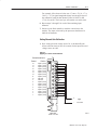
2. Connect shorting links, or apply 0.000mV across each input
channel on the 1771–WI field wiring arm as shown in Figure 6.1.
Figure 6.1
Shorting Inputs for Offset Calibration
$/+(, * #$,1(%(" 1(-,
#
#
#
#
#
#
#
#
'-/1(,& *(,)
$.$ 1 %-/ $ "' "' ,,$*
1
- ,-1
20$
'-/1 $ "' (,.21
-/ ..*3 +
"/-00 $ "' (,.21
"' ,,$*
#
#
#
#
#
#
#
#
,.21 *$
,.21 *$
,.21 *$
,.21 *$
,.21 *$
,.21 *$
,.21 *$
,.21 *$
-1 0$#
-1 20$#
,.21 *$
,.21 *$
,.21 *$
,.21 *$
,.21 *$
,.21 *$
,.21 *$
,.21 *$
2,"1(-,
$/+(, *
..*3
+
(/(,& /+
1 - 3. After the connections stabilize, request the offset calibration by
setting bit 00 in block transfer write word 28 and sending a block
transfer write (BTW) to the module. Refer to Table 6.A.
When the BTW is sent, all channels are calibrated to 0.000mV.
2!*(" 1(-, 4 4 3 Module Calibration
6–3
Table 6.A
Write Block Transfer Word 28
Word
Bit
17 16 15 14 13 12 11 10 07 06 05 04 03
'#$$- %$+-$('
(+ 02
01
00
!*.!,-! .-(%$+-$('
!- -#!,! $-, -( !*.!,-!
/!
%.!,
!*.!,-!
$' %
!*.!,-!
"",!- %
NOTE: Normally, all channels are calibrated simultaneously (bits
10–17 of word 28 are octal 0). To disable calibration on any
channel, set the corresponding bit 10 through 17 of word 28.
4. Queue block transfer reads (BTRs) to monitor for offset
calibration complete and any channels which may have not
calibrated successfully. Refer to Table 6.B.
Table 6.B
Read Block Transfer Word 13
Word
Bit
17 16 15 14 13 12 11 10
07
06
'%$+-! #''!%,
(+ 05 04 03
02
01
00
$' %
(&)%!-!
"",!- %
(&)%!-!
.-(%$+-$(' --.,
%
.%-
.%-
(- .,!
/! -(
(&)%!-!
5. Proceed to Gain Calibration below.
Gain Calibration
Calibrating gain requires that you apply +100.000mV across each
input channel.
Normally all inputs are calibrated together. To calibrate the gain of
an input, proceed as follows:
1. Apply +100.000mV across each input channel as shown in
Figure 6.2.
.%$-$(' 1
1 0 6–4
Module Calibration
Figure 6.2
Applying 100.00mV for Gain Calibration
!*&$'% !',$"$,$('
-',$('
1
( '(,
-+!
')-, %!
')-, %!
')-, %!
')-, %!
')-, %!
')-, %!
')-, %!
')-, %!
(, +!
(, -+!
')-, %!
')-, %!
')-, %!
')-, %!
')-, %!
')-, %!
')-, %!
')-, %!
!*&$'%
+
$*$'# *&
, ( ))%.
&
2. After the connections stabilize, request the gain calibration by
setting bit 01 in BTW word 28 and sending a block transfer write
(BTW) to the module. Refer to Table 6.A.
When the BTW is sent, all channels are calibrated to +100.00mV.
NOTE: Normally, all channels are calibrated simultaneously (bits
10–17 of word 28 are octal 0). To disable calibration on any
channel, set the corresponding bit 10 through 17 of word 28.
3. Queue BTRs to monitor for gain calibration complete and any
channels which may not have calibrated successfully.
Save Calibration Values
If any ”uncalibrated channel” bits (bits 10–17 of word 13) are set, a
save cannot occur. Auto–calibration should be performed again,
starting with offset calibration. If the module has a faulty channel,
the remaining functioning channels can be calibrated by inhibiting
calibration on the faulty channel.
-%$,$(' /
/ . Module Calibration
6–5
The module can be run with the new calibration values, but will lose
them on power down. To save these values, proceed as follows:
1. Request a ”save to EEPROM” by setting bit 02 in BTW word 28
and sending the BTW to the module. Refer to Table 6.A.
2. Queue BTRs to monitor for ”save complete”, ”EEPROM fault”
and ”calibration fault.” An EEPROM fault indicates a
nonoperative EEPROM; a calibration fault indicates at least one
channel was not properly offset or gain calibrated and a save did
not occur.
Performing Manual
Calibration
You calibrate each channel by applying a precision voltage to the
input terminals, comparing correct with actual results, and entering
correction into the corresponding calibration word for that channel.
The correction takes affect after it is transferred to the module by the
corresponding BTW instruction in your ladder diagram program.
Always start with offset adjustment followed by gain adjustment.
Before calibrating the module, you must enter ladder logic into
processor memory, so that you can initiate write block transfers to
the module, and the processor can read inputs from the module.
Write transfers will contain calibration values in words 20 through
27 for the channel you are calibrating.
Use a precision voltage source, such as Data Precision 8200 or
equivalent, for your calibration input voltage.
Setting Channel Offset Calibration
1. Select the millivolt range and binary data format. (BCD could be
used, but it cannot display values larger than 100mV required
during gain calibration.)
2. Apply 0.000 millivolts to the channel input as shown in
Figure 6.3.
6–6
Module Calibration
Figure 6.4
Shorting Inputs for Offset Calibration
$/+(, * #$,1(%(" 1(-,
2,"1(-,
#
#
#
#
#
#
#
#
'-/1(,& *(,)
$.$ 1 %-/ $ "' "' ,,$*
1
- ,-1
20$
'-/1 $ "' (,.21
-/ ..*3 +
"/-00 $ "' (,.21
"' ,,$*
#
#
#
#
#
#
#
#
,.21 *$
,.21 *$
,.21 *$
,.21 *$
,.21 *$
,.21 *$
,.21 *$
,.21 *$
-1 0$#
-1 20$#
,.21 *$
,.21 *$
,.21 *$
,.21 *$
,.21 *$
,.21 *$
,.21 *$
,.21 *$
$/+(, *
..*3
+
(/(,& /+
1 - 3. Observe the input value read by the processor (word 4 of the BTR
file for channel 1). It should be 0000.
4. Multiply the difference between your observed value and 0.000
by 3.0933. Determine the magnitude and sign of the required
correction.
You can adjust the correction up to +127 binary counts
(+410.56µV).
A negative correction means that the reading was too high and
you want to subtract a corrective amount from that reading.
A positive correction means that the reading was too low and you
want to add a corrective amount to that reading.
5. Enter the magnitude and sign of the correction in binary code into
the upper (offset correction) byte of the calibration word for that
channel. (BTW file, word 20, bits 17–10 for channel 1.)
2!*(" 1(-, 4 4 3 Module Calibration
6–7
For example, if the observed value was 17, enter –53 [(0 – 17) x
3.0933 = –53] in signed magnitude binary into the upper byte of
the calibration word for that channel. Enter 10110101 in bits
17–10 of word 20. The lower byte will remain zero at this time.
6. Repeat steps 3 through 5 for each of the remaining input
channels.
7. Initiate a write block transfer to send the corrections to the
module. The input value read by the processor should now be
0000 for all channels.
Setting Channel Gain Calibration
1. Now set the precision voltage source for +100.000 millivolts.
Allow sufficient time (at least 10 seconds) for the input filter and
voltage source to settle.
Figure 6.5
Applying 100.000mV for Gain Calibration
!*&$'% !',$"$,$('
1
( '(,
-+!
')-, %!
')-, %!
')-, %!
')-, %!
')-, %!
')-, %!
')-, %!
')-, %!
(, +!
(, -+!
')-, %!
')-, %!
')-, %!
')-, %!
')-, %!
')-, %!
')-, %!
')-, %!
-',$('
!*&$'%
+
$*$'# *&
, ( ))%.
&
-%$,$(' /
/ . 6–8
Module Calibration
2. Record the input value read by the processor in the BTR file
(word 4 for channel 1). Determine the percentage difference
from 10000 and the sign of the correction.
You can adjust the correction up to +0.19379%.
A negative correction means that the reading was too high and
you want to subtract a corrective amount from that reading.
A positive correction means that the reading was too low and you
want to add a corrective amount to that reading.
If programming in BCD, the upper limit for the display is A000.
If the overrange bit is set, turn back the voltage reference until the
overrange turns off. Use the difference for the calculation.
For example, if the observed value was 10014, then 10000–10014
= –14, and –14 divided by 10000 = –0.14%.
3. Using the following table, select gain correction values that most
nearly add up to the percentage that you determined in step 1.
Select a value only once.
Bit
Value
Enter the bit code representing the sum of the corrections into the
lower byte (gain correction) of the calibration word for that
channel.
For example, to attain the value of 0.140%, you would add:
Percentage
Bit Number
Enter 11011100 in the lower byte of the calibration word for that
channel. This entry would set bits 07 (sign) and 06, 04, 03 and 02
which is –0.1403807, very close to the required –0.14. Remember
to keep the upper byte the same as it was from step 5.
Module Calibration
6–9
4. Repeat the above steps 2 and 3 for channels 2 through 8.
5. Initiate a write block transfer to send the corrections to the
module. The input value read by the processor should now be
10000 (A000 for BCD) for all channels.
6. If the correction changes the result in the wrong direction, change
the sign and reenter it.
Important:
Chapter Summary
If the % correction required is larger than
+0.19379, check your reference voltage. If the
reference voltage is correct, perform
auto–calibration.
In this chapter, you learned how to calibrate your input module.
6–10
Module Calibration
Chapter
7
Chapter Objective
Diagnostics Reported by
the Module
We describe how to troubleshoot your module by observing LED
indicators and by monitoring status bits reported to the processor.
At power–up, the module momentarily turns on both indicators as a
lamp test, then checks for
•
•
•
•
correct RAM operation
EPROM operation
EEPROM operation
a valid write block transfer with configuration data
Thereafter, the module lights the green RUN indicator when
operating without fault, or lights the red FAULT indicator when it
detects fault conditions. If the red FAULT indicator is on, block
transfers will be inhibited.
The module also reports status and specific faults (if they occur) in
every transfer of data to the PC processor. Monitor the green and
red status indicators and status bits in word 1 of the BTR file when
troubleshooting your module.
Figure 7.1
Status Indicators
% # '"!&!$# )
) ( 7–2
Troubleshooting
Troubleshooting with the
Indicators
Table 7.A shows LED indications and probable causes and
recommended actions to correct common faults.
Table 7.A
Troubleshooting Chart for Thermocouple/Millivolt Input
Module (1771-IXE/D)
Probable Cause
Indication
Recommended Action
Both LEDs are OFF
No power to module
Possible short on the module
LED driver failure
Check power to I/O chassis. Recycle as
necessary.
Replace module.
Red FLT LED ON and
Green RUN LED is ON
Microprocessor, oscillator or EPROM failure
Replace module.
Red FLT LED ON
If immediately after power-up, indicates RAM or
EPROM failure.1
Replace module.
If during operation, indicates possible
microprocessor or backplane interface failure.1
Replace module.
Power-up diagnostics successfully completed.
Normal operation.
If LED continues to flash, and write block transfers
(BTW) cannot be accomplished, you have a
possible interface failure.
Replace module.
Green RUN LED is flashing
1 When red LED is on, the watchdog timer has timed out and backplane communications are terminated. Your
monitor
communication.
Status Reported by the
Module
user program should
Status Reported in Word 1
Design your program to monitor status bits in the lower byte of word
1, and to take appropriate action depending on your application
requirements. You may also want to monitor these bits while
troubleshooting with your industrial terminal. The module sets a bit
(1) to indicate it has detected one or more of the following conditions
as shown in Table 7.B.
Table 7.B
Status Reported in Word 1
Word
Bit
Explanation
1
00
Module is powered but has not received its first (configuration) block transfer.
The green LED is flashing.
01
One or more inputs are out of the range for which you configured the module.
02
Module updated its inputs before the processor read them. The RTS interval
timed out before the processor read the data.
03
Not used
04
The module's ambient temperature is below 0oC. Temperature readings will
be inaccurate.
05
The module's ambient temperature is above 60oC. Temperature readings will
be inaccurate.
Word 1
(cont)
Publication 1771Ć6.5.130 Ć May 1999
Troubleshooting
Word
Bit
7–3
Explanation
+/ 0."!
(&-/&+* +*./*/. +0(! *+/ " -"! %" )+!0(" 2&(( +*/&*0" /+
+,"-/" 0/ -"!&*$. )4 " &* 0-/"
&$* &/. #+- " % %**"(
Status Reported in Words 2 and 3
Design your program to monitor over/under range bits, and to take
appropriate action depending on your application requirements. You
may also want to monitor these bits while troubleshooting with your
industrial terminal.
Bits 00–07 and 10–17 each represent an input for channels 1–8,
respectively. For example, bit 04 represents input channel 5. The
module sets a bit (1) to indicate it has detected an out of range
condition. Refer to Table 7.C.
Table 7.C
Status Reported in Words 2 and 3
Word
Bit
Condition
*,0/. 0*!"--*$" &/ &. %**"( &/ &. %**"( # &*,0/ +**" /&+*. *!
1+(/$". -" +--" / /%&. .//0. )4 &*!& /" #&("! %**"( +))0*& /&+*. 2&/%
/%" )& -+,-+ "..+- # (( %**"(. -" 0*!"--*$" /%&. &*!& /". ,+..&(" ! !
+*1"-/"- #&(0-" +- (+2* #0."
*,0/. +1"--*$" &/ &. %**"( &/ &. %**"( # &*,0/ +**" /&+*. *!
1+(/$". -" +--" / /%&. .//0. )4 &*!& /" #&("! /%"-)+ +0,(" #0* /&+*(
*(+$ (+ ' +--".,+*!&*$ %**"( &*,0/ 1(0" &. "(+2 /%" (-) 1(0" /%/ 4+0 "*/"-"! #+/%/ %**"(
+--".,+*!&*$ %**"( &*,0/ 1(0" %. "3 ""!"! /%" (-) 1(0" /%/ 4+0 "*/"-"!
#+- /%/ %**"(
0(& /&+* 5 5 4 7–4
Troubleshooting
Status Reported in Word 13
Design your program to monitor status bits in word 13 during
auto–calibration, and to take appropriate action depending on your
requirements. You may also want to monitor these bits while
troubleshooting with your industrial terminal. The module sets a bit
(1) to indicate it has detected one or more of the following conditions
as shown in Table 7.D.
Table 7.D
Status Reported in Word 13
Word
Bit
#( "#' *%''"
"" & #( "#' %' & "' + '& '%#( %&$') +
Chapter Summary
( '#" ,
, + Condition
' "" '%#( ' "" #( "#' %' *%" %! #""'#"& " &#(% #% $%#$% )# '
In this chapter, you learned how to interpret the LED status
indicators, status words and troubleshoot your input module.
Appendix
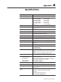
A
Number of Inputs
8, all of the same type or 4 each of 2 different types
I/O Chassis Location
Any single I/O module slot
Type of Input (Selectable)
Type E, chromel/constantan
Type J, iron/constantan
Type K, chromel/alumel
Type R, Pt/Pt-13% Rh
Type T, copper/constantan
Type S, Pt/Pt-10% Rh
Millivolt
Thermocouple Linearization
IPTS-68 standard, NBS MN-125
Cold Junction Compensation
Range: 0 to 60oC
Accuracy: +0.5oC
Temperature Scale (Selectable)
oC or oF
Input Resolution
1oC, 1oF, or 10uV
Input Isolation
1000V peak between inputs, between input and common, and
between input and backplane connections
Common Mode Rejection
120dB at 60Hz, up to 1000V peak
Common Mode Impedance
Greater than 10 megohms
Normal Mode Rejection
60dB at 60Hz
Input Overvoltage Protection
120V rms, continuous
Open Input Detection
Open input produces a maximum value reading in less than 10
seconds
Input Connections
18-terminal wiring arm (Cat. No. 1771-WI)
Data Format (Selectable)
4-digit BCD
2's complement binary
signed magnitude binary
Calibration
Auto-calibration (offset and gain)
Zero offset and gain adjustment for each channel via programming
terminal
Verify every six months for maintaining absolute accuracy
Processor Compatibility
Any A-B processor using the 1771 I/O structure and block transfer
Environmental Conditions
Operating Temperature:
Rate of Change:
Storage Temperature:
Relative Humidity:
(-270 to 1000oC)
(-210 to 1200oC)
(-270 to 1380oC)
(-50 to 1770oC)
(-270 to 400oC)
(-50 to 1770oC)
(-100 to +100mV dc)
0 to 60oC (32 to 140oF)
Ambient changes greater than 0.5oC per minute may temporarily
degrade performance during periods of change
-40 to 85oC (-40 to 185oF)
5 to 95% (without condensation)
Backplane Power Consumption
750mA @ 5V; 3.75 Watts maximum
Field Wiring Arm
Cat. No. 1771-WI
Keying
Between 20 and 22
Between 24 and 26
Agency Certification (when product is
marked)
• CSA certified
• CSA Class I, Division 2, Groups A, B, C, D certified
• UL listed
• CE marked for all applicable directives
• C-Tick marked for all applicable acts
Publication 1771-6.5.130 Ć May 1999
A–2
Specifications
Thermocouple/Millivolt
Input Module Accuracy
The accuracy of your thermocouple readings depends on:
• module accuracy
• lead resistance effect
• accuracy of the thermocouple
The accuracy of the module is shown in NO TAG and NO TAG at
ambient temperature (25oC) and over the temperature range
(0–60oC).
Use the calibration procedure in Chapter 6 to adjust your module to
compensate for your specific environment.
Table A.A
Thermocouple Range Accuracy Based on Temperatures
Above 0oC
Thermocouple
Type
Temperature
Range oC
Max Error @
Calibration
Temperature (25oC)1
Temperature Drift
oC/oC (0-60oC)
or oF/oF (32-140oF)
E
-270 to 1000
+0.74oC/+1.08oF
+0.0400
J
-210 to 1200
+0.78oC/+1.10oF
+0.0423
K
-270 to 1380
+0.77oC/+1.15oF
+0.0640
-270 to 400
+0.77oC/+1.17oF
+0.0183
-50 to 1770
+1.50oC/+2.11oF
+0.0914
-50 to 1770
+1.50oC/+2.31oF
+0.0926
T
R
S
1 Error is specified from 0oC (32oF)
to the maximum range of the thermocouple. Error does
not include thermocouple error (see appendix F).
Table A.B
Millivolt Range Accuracy
Millivolt
Range
Max Error
@ Calibration
Temperature (25oC)
Millivolt Drift
-100 to 100
+8.85uV
+3.856uV/oC
Table A.C
Radiated Noise Susceptibility
Radiated Noise
300-1000MHz Circular Wave, Field Strength = 10V/M
Publication 1771-6.5.130 Ć May 1999
Susceptibility Error
< +1%
Specifications
Lead Resistance
Compensation
A–3
Allowable Distances
The open thermocouple detection circuit injects a current of
approximately 7.3 nanoamps into the thermocouple cable. A total
lead resistance of 1370 ohms (685 ohms one–way) cable resistance
will produce +1 count (10uV) of error.
Source Impedance Compensation for Millivolt Inputs
Source resistance causes similar errors to occur with millivolt inputs.
If source resistance is less than 100 ohms, no compensation is
necessary to maintain stated accuracy. If source resistance is greater
than 100 ohms, the error can be calculated as follows:
&&%& !$ "!&(!%$ %)$(' Where
' !$
' % #'
Rs = source resistance (one–way cable resistance)
Vin = applied input voltage
When using thermocouples, Vin is the approximate thermocouple
voltage of the temperature of interest.
&&%& $(&$"
%)"
!&)!(&*
#% #'
!$
%
To maintain a display error of < 5uV at Vin = OV, RS should be <
341 ohms. Refer to NBS NM–125 Thermocouple Reference Tables
for determining actual thermocouple voltage versus temperature
readings.
Filtering
The analog input module has hardware–based high frequency filters
on all channels to reduce the effect of electrical noise on the input
signal. In addition, a 6–pole digital filter, which begins rolling off at
8.0Hz, is also incorporated.
)"!(!%$ + * A–4
Specifications
Appendix
B
Sample Programs for the
Input Module
PLC-2 Family Processors
The following are sample programs for entering data in the
configuration words of the write block transfer instruction when
using the PLC–2, PLC–3 or PLC–5 family processors.
To enter data in the configuration words, follow these steps. NOTE:
For complete programming sample, refer to Figure 4.1.
Example:
Enter the following rung for a write block transfer:
Power Up Bit
BTW
BLOCK XFER WRITE
DATA ADDR:
030
MODULE ADDR:
110
BLOCK LENGTH:
27
FILE:
400-432
010
EN
06
110
DN
06
400 is the address of the write block transfer data file. You want to
examine configuration word 1.
In RUN/PROG Mode
Action
Result
1. Press [SEARCH]8<data address>
Finds the block address transfer
instruction
2. Press CANCEL COMMAND
Removes preceeding command
3. Press [DISPLAY]0 or 1
Displays the file in binary or BCD
4. Press [SEARCH]51
On line data change
Cursor defaults to first entry in file when
SEARCH 51 is pressed.
5. Press [INSERT]
Writes data to file element
In PROG Mode
Action
Result
1. Press [SEARCH]8<data address>
Finds the block transfer instruction
2. Press CANCEL COMMAND
Removes preceeding command
3. Press [DISPLAY]0 or 1
Displays the file in binary or BCD
4. Press [DISPLAY]001 and enter data
Puts cursor on word 1
5. Press [INSERT]
Publication 1771-6.5.130 Ć May 1999
B–2
Programming Examples
Use the above procedure to enter the required words of the write
block transfer instruction. Be aware that the block length will depend
on the number of channels selected and whether alarming or user
calibration are implemented. For example, the block may contain
only 1 word if no alarming or user calibration are implemented, but
may contain 27 words if using 8 inputs with alarming and user
calibration. The PLC–2 family write block transfer data file should
look like Figure B.1.
Figure B.1
Write Block Transfer Data Transfer for a PLC-2 Family
Processor
! % ! !
$ #!
" !
PLC-3 Family Processors
! !
Following is a sample procedure for entering data in the
configuration words of the write block transfer instruction when
using a PLC–3 processor. For a complete sample program, refer to
Figure Figure 3.2.
To enter data in the configuration words, follow these steps:
Example:
Enter the following rung for a write block transfer:
!#
-2)/".*0
$ #!
"
"
!
!
!
!
!
!
F0003:0000 is the address of the write block transfer data file. You
want to enter/examine word 1.
1'+*(&0*-, 4 &3 Programming Examples
B–3
1.
Press [SHIFT][MODE] to display your ladder diagram on the
industrial terminal.
2.
Press DD,03:0[ENTER] to display the block transfer write file.
The industrial terminal screen should look like Figure B.2. Notice
the highlighted block of zeroes. This highlighted block is the cursor.
It should be in the same place as it appears in Figure B.2. If it is not,
you can move it to the desired position with the cursor control keys.
Once you have the highlighted cursor in the right place, you can go
on to step 3.
3.
Enter the data corresponding to your bit selection in words 0
through 4.
4.
When you have entered your data, press [ENTER]. If you make a
mistake, make sure the cursor is over the word you desire to
change. Enter the correct data and press [ENTER].
Figure B.2
Write Block Transfer for a PLC-3 Processor
!"
5.
PLC-5 Family Processors
! "
Press [CANCEL COMMAND]. This returns you to the ladder
diagram.
The following is a sample procedure for entering data in the
configuration words of the block transfer write instruction when
using a PLC–5 processor. For a complete sample program, refer to
Figure Figure 3.3.
+$'&%#*&)( - #, B–4
Programming Examples
1.
Enter the following rung:
"
#" !
!
!!
.4(0!/+2
+1 2*( $''0(11 .) 2*( " 20$-1)(0 )+,(
2.
Press [F8],[F5] and enter N7:60 to display the configuration
block. The industrial terminal screen should like Figure B.3.
Figure B.3
Sample PLC-5 Data File (Hexadecimal Data)
''0(11
The above data file would configure the module as follow:
•
•
•
•
•
•
•
•
3%,+&$2+.- 6 $5 ”K” thermocouples on all inputs
temperature scale of Celsius
output data in BCD format
real time sampling set to a 1 second scan rate
all channel alarms ON
all channel minimum alarm values set to –40
all channel maximum alarm values set to +85
all calibration values set to 0
3.
Enter the data corresponding to your bit selections and add alarm
and calibration values, if so desired.
4.
[ESC] returns you to the main menu.
Appendix
C
4-Digit Binary Coded
Decimal (BCD)
The 4–digit BCD format uses an arrangement of 16 binary digits to
represent a 4–digit decimal number from 0000 to 9999 (NO TAG).
The BCD format is used when the input values are to be displayed
for operator viewing. Each group of four binary digits is used to
represent a number from 0 to 9. The place values for each group of
digits are 20, 21, 22 and 23 (NO TAG). The decimal equivalent for a
group of four binary digits is determined by multiplying the binary
digit by its corresponding place value and adding these numbers.
Figure C.1
4-Digit Binary Coded Decimal
C–2
Data Table Formats
Table C.A BCD Representation
23 (8)
Signed-magnitude Binary
Place Value
22 (4)
21 (2)
Decimal
Equivalent
20 (1)
Signed–magnitude binary is a means of communicating numbers to
your processsor. It should be used with the PLC–2 family when
performing computations in the processor. It cannot be used to
manipulate binary 12–bit values or negative values.
Example: The following binary number is equal to decimal 22.
101102 = 2210
The signed–magnitude method places an extra bit (sign bit) in the
left–most position and lets this bit determine whether the number is
positive or negative. The number is positive if the sign bit is 0 and
negative if the sign bit is 1. Using the signed magnitude method:
0 10110 = +22
1 10110 = –22
Two's Complement Binary
Two’s complement binary is used with PLC–3 processors when
performing mathematical calculations internal to the processor. To
complement a number means to change it to a negative number. For
example, the following binary number is equal to decimal 22.
101102 = 2210
Data Table Formats
C–3
First, the two’s complement method places an extra bit (sign bit) in
the left–most position, and lets this bit determine whether the
number is positive or negative. The number is positive if the sign bit
is 0 and negative if the sign bit is 1. Using the complement method:
0 10110 = 22
To get the negative using the two’s complement method, you must
invert each bit from right to left after the first ”1” is detected.
In the above example:
0 10110 = +22
Its two’s complement would be:
1 01010 = –22
Note that in the above representation for +22, starting from the right,
the first digit is a 0 so it is not inverted; the second digit is a 1 so it is
not inverted. All digits after this one are inverted.
If a negative number is given in two’s complement, its complement
(a positive number) is found in the same way:
1 10010 = –14
0 01110 = +14
All bits from right to left are inverted after the first ”1” is detected.
The two’s complement of 0 is not found, since no first ”1” is ever
encountered in the number. The two’s complement of 0 then is still 0.
C–4
Data Table Formats
Appendix
D
Block Transfer (Mini-PLC-2
and PLC-2/20 Processors)
Multiple GET Instructions
- Mini-PLC-2 and
PLC-2/20 Processors
Programming multiple GET instructions is similar to block format
instructions programmed for other PLC–2 family processors. The
data table maps are identical, and the way information is addressed
and stored in processor memory is the same. The only difference is
in how you set up block transfer read instructions in your program.
For multiple GET instructions, individual rungs of ladder logic are
used instead of a single rung with a block transfer instruction. A
sample rung using multiple GET instructions is shown in NO TAG
and described in the following paragraphs.
Rung 1: This rung is used to set four conditions.
• Examine On Instruction (113/02) – This is an optional
instruction. When used, block transfers will only be initiated
when a certain action takes place. If you do not use this
instruction, block transfers will be initiated every I/O scan.
• First GET Instruction (030/120) – identifies the module’s
physical address (120) by rack, group and slot; and where in the
accumulated area of the data table this data is to be stored (030).
• Second GET Instruction (130/060) – indicates the address of the
first word of the file (060) that designates where the data will be
transferred. The file address is stored in word 130, 1008 above the
data address.
• Output Energize Instruction (012/07) – enables the block
transfer read operation. If all conditions of the rung are true, the
block transfer read enable bit (07) is set in the output image data
table control byte. The output image table control byte contains
the read enable bit and the number of words to be transferred. The
output energize instruction is defined as follows:
• ”0” indicates that it is an output instruction
• ”1” indicates the I/O rack address
• ”2” indicates the module group location within the rack
• ”07” indicates this is a block transfer read operation (if this
were a block transfer write operation, ”07” would be replaced
by ”06”.)
Rungs 2 and 3: These output energize instructions (012/01 and
012/02) define the number of words to be transferred. This is
accomplished by setting a binary bit pattern in the module’s output
image table control byte. The binary bit pattern used (bits 01 and 02
energized) is equivalent to 6 words or channels, and is expressed as
110 in binary notation.
D–2
Block Transfer (Mini–PLC–2 and PLC–2/20 Processors)
Rung Summary: Once the block transfer read operation is
complete, the processor automatically sets bit 07 in the input image
table status byte and stores the block length of the data transferred.
Figure D.1
Multiple GET Instructions (Mini-PLC-2 and PLC-2/20
Processors Only)
010
Data Table
07
Output
Image Table
Control
Byte
1
012
R
017
1
2
0
Timer/Counter
Accumulated
Values Area
027
030
060
Output Image Table Control
Byte Contains Read
Enable Bit and Block
Length in Binary Code
Data Address
Contains Module
Address in BCD
First Address,
Destination of
Transferred Data
065
07
Input
Image
Table
110
Status
Byte
1
R
0
112
117
6
0
Timer/Counter
Preset
Values Area
130
Input Image Table
Status Byte
Contains Done Bit
Storage Location
Contains File
Address in BCD
R = Read 07 = Bit
12172
Setting the Block Length
(Multiple GET Instructions
only)
" ! The input module transfers a specific number of words in one block
length. The number of words transferred is determined by the block
length entered in the output image table control byte corresponding
to the module’s address.
Block Transfer (Mini–PLC–2 and PLC–2/20 Processors)
D–3
The bits in the output image table control byte (bits 00 – 05) must be
programmed to specify a binary value equal to the number of words
to be transferred.
For example, NO TAG shows if your input module is set up to
transfer 6 words, you would set bits 01 and 02 of the lower image
table control byte. The binary equivalent of 6 words is 000110. You
would also set bit 07 when programming the module for block
transfer read operations. Bit 06 is used when block transfer write
operations are required.
Figure D.2
Setting Block Length (Multiple GET Instructions only)
Block Transfer
Read Enable Bit
1
For Block
Transfer Active
Operations Only
Read 6 Words
from Module
0 0 0 0 1 1
0
010
Data Table
Control
Byte
1
Output Image Table
Output Image Table Control
Byte Contains Read
Enable Bit and Block
Length in Binary Code
012
R
017
1
2
027
030
0
Data Address
Contains Module
Address in BCD
Number of
Words to
Transfer
Binary Bit Pattern
Lower Output Image Table Byte
05
04
03
02
01
00
:
:
D–4
Block Transfer (Mini–PLC–2 and PLC–2/20 Processors)
Appendix
E
Differences Between Series A,
Series B, Series C and Series
D Thermocouple/Millivolt
Input Modules
Major Differences between
Series
The following is a list of major differences between Series A, Series
B, Series C and Series D Thermocouple/Millivolt Input module (cat.
no. 1771–IXE).
Definition
Series A
Series B
Series C and Series D
Calibration
Uses potentiometers for calibration
settings with calibration done at -99 and
+99mV.
Calibration is done automatically using auto-calibration feature, or
manually through programming.
Offset, Gain Calibrations
User offset calibration range of +1270uV.
Offset correction of 3.2328 uV/bit.
User gain correction of .012207%/LSB
with a maximum of 1.5503%.
User offset calibration range is +410.5uV maximum. An offset
correction is 3.2328 uV/bit User gain correction is now
.00152588%/LSB for a maximum of +0.193787%.
Real Time Sampling
Series A default value was 500ms.
The default RTS setting (RTS = 0) makes data available every
50ms.
Cold Junction Calibration
In Series A, BTR word 12 was the cold
junction calibration word.
BTR WORD 12 is the rounded Cold Junction Temperature resolute
to 1 degree C displayable in the programmed format (BCD, 2s
complement or signed magnitude).
Cold Junction calibration done by user.
Cold Junction calibration automatically calibrated at power up.
Cold junction temperature is updated
once per 15 second interval.
Cold junction temperature is digitally filtered with a filter time
constant of 12.8 seconds.
Cold junction value is updated continously
High and Low Alarms Limits
When a low alarm is programmed greater When a low alarm is programmed greater than a high alarm both
than a high alarm, the Series A displayed low and high alarms will be activated when the input is between
only low alarm.
the two values.
Backplane Current
1200mA at 5V.
Agency Certification
(when product or packaging is
marked)
• CSA certified
• CSA Class I, Division 2, Groups A, B, C, D certified
• UL listed
750mA at 5V.
850mA at 5V.
• CSA certified
• CSA Class I, Division 2, Groups A, B,
C, D certified
• UL listed
• CE marked for all applicable directives
Publication 1771-6.5.130 Ć May 1999
E–2
Differences Between Series A, Series B, Series C and Series D Thermocouple/Millivolt
Explanation of Differences
• Calibration is now done automatically using auto–calibration
•
•
•
•
•
•
•
•
•
•
•
feature, or manually through programming.
calibration is now done at 0.000mV and +100.000mV .
If EEPROM read of the auto cal values fails, BTR WORD 1 bit 7
is asserted.
Series A used potentiometers for calibration settings with
calibration done at –99 and +99mV.
RTS can now be reduced to 100ms for all thermocouples by
programming RTS = 1.
The default RTS setting (RTS = 0) makes data available every
50ms. Series A default value was 500ms.
BTR WORD 12 is the rounded Cold Junction Temperature
resolute to 1 degree C displayable in the programmed format
(BCD, 2s complement or signed magnitude). In Series A, BTR
word 12 was the cold junction calibration word.
BTW WORD 1 bit 7 is no longer used (cold junction
update).
Cold Junction calibration by the user is no longer required; it is
calibrated at power up.
Cold junction temperature is digitally filtered having a filter
time constant of 12.8 seconds. It is no longer updated once per 15
second interval.
Cold junction value is updated continously in Series B. Update
was once every 15 seconds in Series A.
Backplane power is approximately 750mA at 5V. Series A had a
backplane power requirement of 1200mA.
Differences Between Series A, Series B, Series C and Series D Thermocouple/Millivolt
E–3
• Accuracy specifications over typical RANGES and
TEMPERATURES are:
Input Type
Range IS
!
Range WAS
"!
Accuracy IS
!
!
"!
"! !
"! !
!
"! !
"! !
!
"! !
"! !
!
"! !
"! !
!
"! !
"! !
!
#
NOTE: Measurements of the most negative temperature extremes
are less accurate, as the Seebeck coefficient of the thermocouple
drops below the input resolution of the module, 3.2328uV/bit.
Above specifications are valid to ?degrees on thermocouple types ?
and ?.
• User offset calibration range is +410.5uV maximum. Series A
•
•
•
•
•
•
•
•
was +1270uV. An offset correction is 3.2328 uV/bit not
10uV/bit. User gain correction is now .00152588%/LSB for a
maximum of +0.193787%. Series A was .012207%/LSB with a
maximum of 1.5503%.
Multiple BTRs may occur before configuration of the module.
A block transfer read request with a word length of 00 will
return with the old Series A block transfer default length (27 for a
write; 12 for a read). To access the auto calibration word, the
block transfer length must be set to 28 for a write and 13 for a
read.
Auto calibration can be performed on all channels
simultaneously or on only certain channels of interest. In either
case, channels being calibrated must be connected to the
precision voltage source. Input impedance > 10
Megohms/channel.
When a low alarm is programmed greater than a high alarm both
low and high alarms will be activated when the input is between
the two values. The Series A displayed only low alarm.
An invalid alarm entry (only 0–9 BCD accepted) will cause the
alarm value to be set equal to zero.
In mV mode when displaying in 2’s complement or signed
magnitude format, the module will continue to display readings
past the over or under range limit until the input saturates.
The module employs a digital filter capable of 120dB/decade
rolloff from a corner frequency of 8 Hz.
This Series B module is NOT compatible with the 1771–EX
extender board. Use the 1771–EZ extender board with Series B.
#"! % $ E–4
Differences Between Series A, Series B, Series C and Series D Thermocouple/Millivolt
• The Series B module requires approximately 2 seconds to
•
•
•
•
•
•
execute initialization after power is applied.
The red LED will be turned on and the green LED
extinguished when the watchdog timer times out.
A type code of 1112 will yield S type thermocouple.
Data format of 112 yields signed magnitude instead of 2’s
complement.
When the module is programmed for RTS = 0, and the PLC is
switched from run to program and back to run, an RTS timeout
is inhibited on the switch from program to run.
Allowable ambient temperature change to maintain accuracy is
0.5oC/min.
Series B, C and D have CE certification.
Appendix
F
Thermocouple Restrictions
(Extracted from NBS
Monograph 125 (IPTS-68))
General
Following are some restrictions extracted from NBS Monograph 125
(IPTS–68) issued March 1974 on thermocouples J, K, T, E, R and S:
J (Iron vs Copper-Nickel <Constantan*>) Type Thermocouple
The J thermocouple “is the least suitable for accurate thermometry
because there are significant nonlinear deviations in the
thermoelectric output from different manufacturers. ... The total and
specific types of impurities that occur in commercial iron change
with time, location of primary ores, and methods of smelting.”
“Type J thermocouples are recommended by the ASTM [1970] for
use in the temperature range from 0 to 760C in vacuum, oxidizing,
reducing or inert atmospheres. If used for extended times above
500C, heavy gage wires are recommended because the oxidation rate
is rapid at elevated temperatures.”
“They should not be used in sulfurous atmospheres above 500C.
Because of potential rusting and embrittlement, they are not
recommended for subzero temperatures. They should not be cycled
above 760C even for a short time if accurate readings below 760C
are desired at a later time.”
“The negative thermoelement, a copper–nickel alloy, is subject to
substantial composition changes under thermal neutron irradiation,
since copper is converted to nickel and zinc.”
“Commercial iron undergoes a magnetic transformation near 769C
and <an alpha – gamma> crystal transformation near 910C. Both of
these transformations, especially the latter, seriously affect the
thermoelectric properties of iron, and therefore, the Type J
thermocouples. ... If Type J thermocouples are taken to high
temperatures, especially above 900C, they will lose accuracy of their
calibration when they are recycled to lower temperatures.”
F–2
Thermocouple Restrictions
“ASTM Standard E230–72 in the Annual Book of ASTM Standards
[1972] specifies that the standard limits of error for Type J
commercial thermocouples be +/–2.2C between 0 and 277C and
+/–3/4 percent between 277 and 760C. Limits of error are not
specified for Type J thermocouples below 0C or above 760C. Type J
thermocouples can also be supplied to meet special limits of error,
which are equal to one half the limits given above. The
recommended upper temperature limit for protected thermocouples,
760C, applies to AWG 8 (3.3mm) wire. For smaller wires the
recommended upper temperature decrease to 593C for AWG 14
(1.6mm), and 371C for AWG 24 or 28 (0.5 or 0.3mm).
K (Nickel-Chromium vs Nickel-Aluminum) Type Thermocouple
“This type is more resistant to oxidation at elevated temperatures
than the Types E, J or T thermocouples and consequently it finds
wide application at temperatures above 500C.”
“Type K thermocouples may be used at” liquid hydrogen
“temperatures. However, their Seebeck coefficient (about 4uV/K at
20K) is only about one–half of that of Type E thermocouples.
Furthermore, the thermoelectric homogeneity of KN thermoelements
is generally not quite as good as that of EN thermoelements. Both
the KP and the KN thermoelements do have a relatively low thermal
conductivity and good resistance to corrosion in moist atmospheres
at low temperatures.”
“Type K thermocouples are recommended by the ASTM [1970] for
continuous use at temperatures within the range –250 to 1260C in
oxidizing or inert atmospheres. Both the KP and the KN
thermoelements are subject to oxidation when used in air above
about 850C, but even so, Type K thermocouples may be used at
temperatures up to about 1350C for short periods with only small
changes in calibration.”
“They should not be used in sulfurous, reducing, or alternately
reducing and oxidizing atmospheres unless suitably protected with
protecting tubes. They should not be used in vacuum (at high
temperatures) for extended times because the Chromium in the
positive thermoelement vaporizes out of solution and alters the
calibration. They should also not be used in atmospheres that
promote ”green–rot” corrosion (those with low, but not negligible,
oxygen content).”
Thermocouple Restrictions
F–3
“ASTM Standard E230–72 in the Annual Book of ASTM Standards
[1972] specifies that the standard limits of error for Type K
commercial thermocouples be +/–2.2C between 0 and 277C and
+/–3/4 percent between 277 and 1260C. Limits of error are not
specified for the Type K thermocouples below 0C. Type K
thermocouples can also be supplied to meet special limits of error,
which are equal to one half the standard limits of error given above.
The recommended upper temperature limit for protected Type K
thermocouples, 1260C, applies for AWG 8 (3.3mm) wire. For
smaller wires it decreases to 1093C for AWG 14 (1.6mm), 982C for
AWG 20 (0.8mm), and 871C for AWG 24 or 28 (0.5 or 0.3mm).”
T (Copper vs Copper-Nickel <Constantan*>) Type Thermocouple
“The homogeneity of most Type TP and TN (or EN) thermoelements
is reasonably good. However, the Seebeck coefficient of Type T
thermocouples is moderately small at subzero temperatures (about
5.6uV/K at 20K), being roughly two–thirds that of Type E
thermocouples. This, together with the high thermal conductivity of
Type TP thermoelements, is the major reason why Type T
thermocouples are less suitable for use in the subzero range than
Type E thermocouples.”
“Type T thermocouples are recommended by the ASTM [1970] for
use in the temperature range from –184 to 371C in vacuum or in
oxidizing, reducing or inert atmospheres. The recommended upper
temperature limit for continuous service of protected Type T
thermocouples is set at 371C for AWG 14 (1.6mm) thermoelements,
since Type TP thermoelements oxidize rapidly above this
temperature. However, the thermoelectric properties of Type TP
thermoelements are apparently not grossly affected by oxidation
since Roeser and Dahl [1938] observed negligible changes in the
thermoelectric voltage of Nos. 12, 18, and 22 AWG Type TP
thermoelements after heating for 30 hours in air at 500C. At this
temperature the Type TN thermoelements have good resistance to
oxidation and exhibit only small changes in thermal emf with long
exposure in air, as shown by the studies of Dahl [1941].” ...
“Operation of Type T thermocouples in hydrogen atmospheres at
temperatures above about 370C is not recommended since severe
embrittlement of the Type TP thermoelements may occur.”
“Type T thermoelements are not well suited for use in nuclear
environments, since both thermoelements are subject to significant
changes in composition under thermal neutron irradiation. The
copper in the thermoelement is converted to nickel and zinc.”
F–4
Thermocouple Restrictions
“Because of the high thermal conductivity of Type TP
thermoelements, special care should be exercised in the use of the
thermocouples to insure that both the measuring and reference
junctions assume the desired temperatures.”
ASTM Standard E230–72 in the Annual Book of ASTM Standards
[1972] specifies that the standard limits of error for Type T
commercial thermocouples be +/–2 percent between –101 and –59C,
+/–.8C between –59 and 93C and +/–3/4 percent between 93 and
371C. Type T thermocouples can also be supplied to meet special
limits of error, which are equal to one half the standard limits of
error given above (plus a limit of error of +/–1 percent is specified
between –184 and –59C). The recommended upper temperature limit
for protected Type T thermocouples, 371C, applies to AWG 14
(1.6mm) wire. For smaller wires it decreases to 260C for AWG 20
(0.8mm) and 240C for AWG 24 or 28 (0.5 or 0.3mm).
E (Nickel-Chromium vs Copper-Nickel <Constantan*>) Type
Thermocouple
“Type E thermocouples are recommended by the ASTM Manual
[1970] for use in the temperature range from –250 to 871C in
oxidizing or inert atmospheres. The negative thermoelement is
subject to deterioration above about 871C, but the thermocouple may
be used up to 1000C for short periods.”
“The ASTM Manual [1970] indicates the following restrictions .. at
high temperatures. They should not be used in sulfurous, reducing or
alternately reducing and oxidizing atmospheres unless suitably
protected with protecting tubes. They should not be used in vacuum
(at high temperatures) for extended times, because the Chromium in
the positive thermoelement vaporizes out of solution and alters the
calibration. They should also not be used in atmospheres that
promote ”green–rot” corrosion (those with low, but not negligible,
oxygen content).”
“The negative thermoelement, a copper–nickel alloy, is subject to
composition changes under thermal neutron irradiation since the
copper is converted to nickel and zinc.”
Thermocouple Restrictions
F–5
“ASTM Standard E230–72 in the Annual Book of ASTM Standards
[1972] specifies that the standard limits of error for the Type E
commercial thermocouples be +/–1.7C between 0 and 316C and
+/–1/2 percent between 316 and 871C. Limits of error are not
specified for Type E thermocouples below 0C. Type E
thermocouples can also be supplied to meet special limits of error,
which are less than the standard limits of error given above:
+/–1.25C between 0 and 316C and +/–3/8 percent between 316 and
871C. The recommended upper temperature limit for protected
thermocouples, 871C, applies to AWG 8 (3.3mm) wire. For smaller
wires the recommended upper temperature decreases to 649C for
AWG 14 (1.6mm), 538C for AWG 20 (.8mm) and 427C for AWG 24
or 28 (0.5 or 0.3mm).
S (Platinum-10% Rhodium vs Platinum) & R (Platinum-13%
Rhodium vs Platinum) Type Thermocouples
“The ASTM manual STP 470 [1970] indicates the following
restrictions on the use of S {and R} type thermocouples at high
temperatures: They should not be used in reducing atmospheres, nor
in those containing metallic vapor (such as lead or zinc), nonmetallic
vapors (such as arsenic, phosphorous or sulfur) or easily reduced
oxides, unless suitably protected with nonmetallic protecting tubes.
They should never be inserted directly into a metallic primary tube.”
“The positive thermoelement, platinum–10% rhodium {13%
rhodium for R}, is unstable in a thermal neutron flux because the
rhodium converts to palladium. The negative thermoelement, pure
platinum, is relatively stable to neutron transmutation. However, fast
neutron bombardment will cause physical damage, which will
change the thermoelectric voltage unless it is annealed out.”
“The thermoelectric voltages of platinum based thermocouples are
sensitive to their heat treatments. In particular, quenching from high
temperatures should be avoided.”
“ASTM Standard E230–72 in the Annual Book of ASTM Standards
[1972] specifies that the standard limits of error for Type S {and R}
commercial thermocouples be +/–1.4C between 0 and 538C and
+/–1/4% between 538 and 1482C. Limits of error are not specified
for Type S {or R} thermocouples below 0C. The recommended
upper temperature limit for continuous use of protected
thermocouples, 1482C, applies to AWG 24 (0.5mm) wire.
* It should be noted that the Constantan element of Type J
thermoelements is NOT interchangeable with the Constantan
element of Types T or N due to the different ratio of copper and
nickel in each.
F–6
Thermocouple Restrictions
Index
.+1 !+(.'#'! -" &(.% $)%' (''-(+ $1#'! #',-%%#'! -" &(.% #-(+ ,+#)-#(', #'-+)+-#'! -" ,--., #'#-(+,
%($ -+', + %($ -+', + )+(!+&&#'! %($ -+', + + #-/(+ ,+#)-#(', /(+ ,,#!'&'-,
$1#'! -" $)%' '.% %#+-#(' &(.% !+(.'#'! % %'!-", &(.% #',-%%-#(' %.%-#'! )(/+ +*.#+&'-, &(.% %(-#(' #' ",,#, %#+-#('
"''% ( ,- )+(.+ (+ -((%, &(.% )%&'- (&&.'#-#(' "(/ - #,
-+', ++ '(#, #'-+ +' (' #!.+#'! 1(.+ &(.%
-.+, (' #!.+-#(' %($ (''-#'! /#+#'! )(/+ +*.#+&'-, +(& $)%' +#',-%%-#(' (',#+-#(', -+&#'#'! &(.% )%&'- #!'(,-#,
#'#-(+, +)(+- 1 &(.% #%-+#'! +(!+&&#'! 0&)%
% -#& ,&)%#'! #- ,--#'!, +(&&' % %'!-", I–2
Index
#!" " " "!
#$" #"
# !""#! " ! #$" #"
# "# ! $" #" $!
" % "! 11+3?7'*1+>
:(1/)'9/43 74(1+2 +5479
, >4: ,/3* ' 574(1+2 </9. 4:7 *4):2+39'9/43 51+'8+ )4251+9+ '3* 7+9:73 9./8 ,472
Thermocouple/RTD Input Module User Manual
:( '2+
'9 4
1771-IXE Series D :( 4
Check Problem(s) Type:
1771-6.5.130
:( '9+
May 1999
'79 4
Describe Problem(s):
955132-11
Internal Use Only
"+).3/)'1 )):7')>
9+=9
4251+9+3+88
574)+*:7+89+5
/11:897'9/43
*+,/3/9/43
/3,4 /3 2'3:'1
+='251+
-:/*+1/3+
,+'9:7+
'))+88/(/1/9>
+=51'3'9/43
49.+7
$.'9 /3,472'9/43 /8 2/88/3-
/11:897'9/43
/3,4 349 /3 2'3:'1
1'7/9>
$.'9 /8 :3)1+'7
!+6:+3)+
$.'9 /8 349 /3 9.+ 7/-.9 47*+7
9.+7 422+398
#8+ (')0 ,47 247+ )422+398
&4:7 '2+
4)'9/43.43+
+9:73 94 '70+9/3- 422:3/)'9/438 11+3?7'*1+> 4 11+3?7'*1+> 7/;+ '>,/+1* 98 ?
.43+ ?
% ?
:(1/)'9/43 ??:-:89 ?
NO POSTAGE
NECESSARY
IF MAILED
IN THE
UNITED STATES
BUSINESS
REPLY MAIL
FIRST-CLASS MAIL PERMIT NO. 18235 CLEVELAND OH
1 ALLEN BRADLEY DR
MAYFIELD HEIGHTS OH 44124-9705
-!&%" ,%)( / / . ,$#* )''#(,+
AllenĆBradley, a Rockwell Automation Business, has been helping its customers improve
productivity and quality for more than 90 years. We design, manufacture and support a broad
range of automation products worldwide. They include logic processors, power and motion
control devices, operator interfaces, sensors and a variety of software. Rockwell is one of the
world's leading technology companies.
Worldwide representation.
Argentina • Australia • Austria • Bahrain • Belgium • Brazil • Bulgaria • Canada • Chile • China, PRC • Colombia • Costa Rica • Croatia • Cyprus • Czech Republic • Denmark •
Ecuador • Egypt • El Salvador • Finland • France • Germany • Greece • Guatemala • Honduras • Hong Kong • Hungary • Iceland • India • Indonesia • Ireland • Israel • Italy •
Jamaica • Japan • Jordan • Korea • Kuwait • Lebanon • Malaysia • Mexico • Netherlands • New Zealand • Norway • Pakistan • Peru • Philippines • Poland • Portugal • Puerto
Rico • Qatar • Romania • Russia-CIS • Saudi Arabia • Singapore • Slovakia • Slovenia • South Africa, Republic • Spain • Sweden • Switzerland • Taiwan • Thailand • Turkey •
United Arab Emirates • United Kingdom • United States • Uruguay • Venezuela • Yugoslavia
AllenĆBradley Headquarters, 1201 South Second Street, Milwaukee, WI 53204 USA, Tel: (1) 414 382Ć2000 Fax: (1) 414 382Ć4444
Publication 1771-6.5.130 Ć May 1999
Supersedes Publication 1771-6.5.77 Ć January 1991
PN955132-11
Copyright
1999 AllenĆBradley
Company,ĆInc.
Publication
1771-6.5.130
MayPrinted
1999in USA