1
OCTAGON SYSTEMS
Embedded PCs For Extreme Environments
PC–680 User’s Manual
5474 (0406)
DiskOnChip® is a registered trademark of M–Systems. LynxOS® is a registered
trademark of Lynx Real–Time Systems, Inc. Micro PC™, PC SmartLink™, Octagon
Systems Corporation®, the Octagon logo and the Micro PC logo are trademarks of
Octagon Systems Corporation. PICO FA™ is a trademark of Phoenix Technologies Ltd.
QuickBASIC® is a registered trademark of Microsoft Corporation. QNX® is a
registered trademark of QNX Software Systems Ltd. ROM–DOS™ is a trademark of
Datalight. Windows 98™, Windows NT™, and Windows CE™ are trademarks of
Microsoft Corporation.
Copyright 2000, 2003, 2005, 2006—Octagon Systems Corporation. All rights reserved.
However, any part of this document may be reproduced, provided that Octagon Systems
Corporation is cited as the source. The contents of this manual and the specifications
herein may change without notice.
The information contained in this manual is believed to be correct. However, Octagon
assumes no responsibility for any of the circuits described herein, conveys no license
under any patent or other right, and makes no representations that the circuits are free
from patent infringement. Octagon makes no representation or warranty that such
applications will be suitable for the use specified without further testing or modification.
Octagon Systems Corporation general policy does not recommend the use of its products
in life support applications where the failure or malfunction of a component may directly threaten life or injury. It is a Condition of Sale that the user of Octagon products
in life support applications assumes all the risk of such use and indemnifies Octagon
against all damage.
Technical support: 303–426–4521
6510 W. 91st Ave.
Westminster, CO 80030
Telephone: 303–430–1500
FAX: 303–426–8126
Web site: www.octagonsystems.com
PC-680 user’s manual
Notice to user
IMPORTANT!
Please read the following section before installing your product:
Octagon’s products are designed to be high in performance while consuming very little power. In order to maintain this advantage, CMOS circuitry
is used.
CMOS chips have specific needs and some special requirements that the
user must be aware of. Read the following to help avoid damage to your
card from the use of CMOS chips.
≡ Using CMOS circuitry in industrial control
Industrial computers originally used LSTTL circuits. Because many
PC components are used in laptop computers, IC manufacturers are
exclusively using CMOS technology. Both TTL and CMOS have
failure mechanisms, but they are different. Described below are some
of the failures which are common to all manufacturers of CMOS
equipment. However, much of the information has been put in the
context of the Micro PC.
Octagon has developed a reliable database of customer-induced, field
failures. The average MTBF of Micro PC cards exceeds 11 years, yet
there are failures. Most failures have been identified as customerinduced, but there is a small percentage that cannot be identified. As
expected, virtually all the failures occur when bringing up the first
system. On subsequent systems, the failure rate drops dramatically.
Approximately 20% of the returned cards are problem-free. These
cards, typically, have the wrong jumper settings or the customer
has problems with the software. This causes frustration for the
customer and incurs a testing charge from Octagon.
Of the remaining 80% of the cards, 90% of these cards fail due to
customer misuse and accident. Customers often cannot pinpoint
the cause of the misuse.
Therefore, 72% of the returned cards are damaged through some
type of misuse. Of the remaining 8%, Octagon is unable to determine the cause of the failure and repairs these cards at no charge
if they are under warranty.
Notice to user
PC-680 user’s manual
The most common failures on CPU cards are over voltage of the
power supply, static discharge, and damage to the serial and parallel
ports. On expansion cards, the most common failures are static
discharge, over voltage of inputs, over current of outputs, and misuse
of the CMOS circuitry with regards to power supply sequencing. In
the case of the video cards, the most common failure is to miswire the
card to the flat panel display. Miswiring can damage both the card
and an expensive display.
Multiple component failures - The chance of a random component failure is very rare since the average MTBF of an Octagon
card is greater than 11 years. In a 7 year study, Octagon has never
found a single case where multiple IC failures were not caused by
misuse or accident. It is very probable that multiple component
failures indicate that they were user-induced.
Testing “dead” cards - For a card that is “completely nonfunctional”, there is a simple test to determine accidental over voltage,
reverse voltage or other “forced” current situations. Unplug the
card from the bus and remove all cables. Using an ordinary digital
ohmmeter on the 2,000 ohm scale, measure the resistance between
power and ground. Record this number. Reverse the ohmmeter
leads and measure the resistance again. If the ratio of the resistances is 2:1 or greater, fault conditions most likely have occurred.
A common cause is miswiring the power supply.
Improper power causes catastrophic failure - If a card has
had reverse polarity or high voltage applied, replacing a failed
component is not an adequate fix. Other components probably
have been partially damaged or a failure mechanism has been
induced. Therefore, a failure will probably occur in the future.
For such cards, Octagon highly recommends that these cards be
replaced.
Other over-voltage symptoms - In over-voltage situations, the
programmable logic devices, EPROMs and CPU chips, usually fail
in this order. The failed device may be hot to the touch. It is
usually the case that only one IC will be overheated at a time.
Power sequencing - The major failure of I/O chips is caused by
the external application of input voltage while the Micro PC
power is off. If you apply 5V to the input of a TTL chip with the
power off, nothing will happen. Applying a 5V input to a CMOS
card will cause the current to flow through the input and out the
5V power pin. This current attempts to power up the card. Most
inputs are rated at 25 mA maximum. When this is exceeded, the
chip may be damaged.
Failure on powerup - Even when there is not enough current to
destroy an input described above, the chip may be destroyed when
the power to the card is applied. This is due to the fact that the
input current biases the IC so that it acts as a forward biased
PC-680 user’s manual
Notice to user
diode on powerup. This type of failure is typical on serial interface chips.
Under rated power supply: The board may fail to boot due to an
under rated power supply. It is important that a quality power
supply be used with the PC–680 that has sufficient current capacity, line and load regulation, hold up time, current limiting, and
minimum ripple. The power supply for the PC–680 must meet the
startup risetime requirements specified in the ATX Power Design
Guide, version 1.1, section 3.3.5. This ensures that all the circuitry
on the PC-680 sequences properly and avoids system lockup.
Excessive signal lead lengths - Another source of failure that
was identified years ago at Octagon was excessive lead lengths on
digital inputs. Long leads act as an antenna to pick up noise.
They can also act as unterminated transmission lines. When 5V is
switch onto a line, it creates a transient waveform. Octagon has
seen submicrosecond pulses of 8V or more. The solution is to
place a capacitor, for example 0.1 µF, across the switch contact.
This will also eliminate radio frequency and other high frequency
pickup.
≡ Avoiding physical damage to the heatsink/CPU
WARNING!
When handling any Octagon CPU card, extreme care must be
taken not to strike the heatsink (if installed) against another
object, such as a table edge. Also, be careful not to drop the CPU
card, since this may cause damage to the heatsink or CPU as well.
Note
Any physical damage to the CPU control card is not covered under
warranty.
Abbreviations and terms used in this manual
PC–680 user’s manual
Abbreviations and terms used in
this manual
Throughout this manual, the following symbols and terms are used:
xii
Autoexecution
Automatic execution of a program on powerup or
reset.
BIOS
Basic Input Output System. Detailed instructions
that activate peripheral devices. See ROM–DOS.
BIOS drive
The solid–state disk which contains the system
BIOS and ROM–DOS.
bpp
bits per pixel
Console port
Video card or COM1 where BIOS and DOS messages appear and keyboard input is available.
DRAM
Dynamic Random Access Memory devices. DRAMs
provide volatile memory with unlimited read and
write cycles.
Expansion card
The expansion cards add I/O functions to the Micro
PC system, such as analog input/output, digital
input/output, motion control, and display.
Flash
Electrically erasable PROM which allows at least
100,000 write cycles.
h
The suffix “h” denotes a hexadecimal number. A
decimal number has no prefix or suffix. For example, 1000h and 4096 are equivalent.
KB
Kilobyte (1,024 8–bit bytes).
MB
Megabyte (1,048,576 8–bit bytes).
Memory device
The type of static RAM, DRAM, flash memory, or
EPROM specified for either volatile or nonvolatile
memory.
PC/104
expansion
An expansion bus used for holding 8– and 16–bit
expansion cards.
PC Video
A feature on the PC–680 which imports an external
video source into the virtual graphics array (VGA)
system. This feature allows for advanced video
connections including video overlays.
FlashFX
Datalight’s flash file system used to access SSDs
from DOS as a read/write DOS drive.
ROM
Read Only Memory devices. ROMs provide non-
PC–680 user’s manual
Abbreviations and terms used in this manual
volatile memory, have a limited number of write
cycles, and include EPROMs and EEPROMs.
ROM–DOS
Operating system included in Micro PC ROM.
Single board
computer
A printed circuit board that contains a complete
computer: CPU, memory, I/O, and clock. The single
board computer controls the operation of all the
expansion cards.
Solid–state disk
state
(SSD)
A simulated disk which uses a high speed solid–
SRAM
Static Random Access Memory device. SRAMs
provide volatile memory with unlimited read and
write cycles. They may be used with a backup
battery.
Terminal
emulator
A serial communications software package
designed to simulate a terminal required to gain
access to another computer.
TTL compatible
Transistor transistor logic compatible; 0–5V logic
levels.
Virtual drive
A disk created in DOS or extended memory which
emulates an actual disk. The virtual drive provides
temporary storage for files. When power to the
computer is turned off the virtual drive disappears.
W[ – ]
Denotes a jumper block and the pins to connect.
XMODEM
A communications protocol which allows transfer
of files between two computers.
XON/XOFF
A communications protocol for asynchronous
connections. The receiver can pace the sender by
sending the XOFF and XON characters to stop and
continue the data flow.
+5V Safe
+5V at the I/O connectors that is protected by a
0.75A fuse.
memory device. For example, flash memory,
EEPROM, or static RAM.
xiii
Conventions used in this manual
PC–680 user’s manual
Conventions used in this manual
This section explains the format used for notes, warnings, and command entry.
≡ Notes and warnings
Special notes and warnings appear in this manual. Each one has a
different meaning and format. They are as follows:
Note
A note is supplementary or background information. At other times,
it is a hint or reminder that makes a task easier or quicker.
WARNING!
A warning gives vital information. Failure to heed a warning may
cause system failure, equipment damage, or bodily harm to the
system operator.
≡ Command format and procedures
For some commands, you will only enter a single keyword (for example, reset). For most commands, however, you will enter several
keywords followed by one or more parameters for which you must
supply values.
Commands must be entered in a specific format. To indicate the
format, this manual uses a series of conventions that are explained
below. The conventions cover the rules for issuing all commands,
including the most complex ones. Most commands, however, are much
simpler.
The command format looks like this:
command [type_this | or_ this] input {optional_input}
Follow these rules and conventions:
Information which appears on your screen is shown in a different
type face, for example:
PhoenixBIOS 4.0 Release 6.0
Copyright 1985-1998 Phoenix Technologies Ltd.
All Rights Reserved
xiv
PC–680 user’s manual
Conventions used in this manual
Octagon Release: VX.14B-2/3/00
Commands that you must key in are shown in Courier Bold, for
example:
C:> RESET
Italicized refers to information that is specific to your particular
system or program, e.g.,
Enter filename means enter the name of your file.
Paired angle brackets are used to indicate a specific key on your
keyboard, e.g., <ESC> means the escape key; <CTRL> means the
control key; <F1> means the F1 function key.
All addresses are given in hexadecimal, for example, 328h.
xv
PC–680 user’s manual
About this manual
About this manual
The PC–680 user’s manual provides information about installing and
configuring the PC–680. This manual is divided into four sections:
Section 1 — Installation
Chapter 1:
Overview
Chapter 2:
Quick start
Chapter 3:
SETUP programs
Chapter 4:
Save and run programs
Section 2 — Hardware
Chapter 5:
Serial ports
Chapter 6:
LPT1 parallel port
Chapter 7:
Console devices
Chapter 8:
SSDs, DRAM, and battery backup
Chapter 9:
External drives
Chapter 10:
Digital I/O
Chapter 11:
CRTs and flat panels
Chapter 12:
PC/104 expansion
Chapter 13:
Ethernet
Chapter 14:
USB
Section 3 — System management
Chapter 15:
Watchdog timer and hardware reset
Chapter 16:
Serial EEPROM and CMOS RAM
Chapter 17:
User-defined jumper
Chapter 18:
CPU power management
Chapter 19:
Troubleshooting
Section 4 — Appendices
Appendix A: Technical data
Appendix B: Software utilities
Appendix C: Third party support
Appendix D: Accessories
Appendix E: Operation in severe environments
PC-680 user’s manual
Contents
Contents
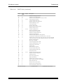
Using CMOS circuitry in industrial control ................................................. 1
Avoiding physical damage to the heatsink/CPU ........................................... 3
Contents
....................................................................................................... iii
List of figures ....................................................................................................... ix
List of tables ..........................................................................................................x
Abbreviations and terms used in this manual ........................................... xii
Conventions used in this manual ................................................................xiv
Notes and warnings ...................................................................................... xiv
Command format and procedures ............................................................... xiv
About this manual .............................................................................................. xix
Overview:
Section 1 – Installation .......................................................... xxi
Chapter 1:
Overview ................................................................................... 1-1
Description ....................................................................................................1-1
PC–680 major hardware features ................................................................1-1
CPU ........................................................................................................ 1-1
Up to 128 MB SDRAM ......................................................................... 1-1
Solid–state disks .................................................................................. 1-1
SSD0 ............................................................................................. 1-2
SSD1 ............................................................................................. 1-2
Floppy and hard disk ports ................................................................. 1-2
Boot sequence ....................................................................................... 1-2
Serial ports protected against ESD ................................................... 1-2
Multifunctional printer port ............................................................... 1-3
Keypad and LCD display support for low cost operator
interface .......................................................................................... 1-3
32–bit digital I/O with versatile configuration ................................. 1-3
USB ........................................................................................................ 1-3
PCI bus XVGA, flat panel interface, and GUI accelerator............... 1-4
Adjustable display bias supply ...........................................................1-4
Speaker, keyboard, and mouse ports .................................................. 1-4
PC/104 16–bit interface ........................................................................ 1-4
Ethernet ................................................................................................ 1-4
Watchdog timer added for safety ....................................................... 1-5
Hardware reset .................................................................................... 1-5
Real time calendar/clock with battery–backup ................................ 1-5
5 Volt operation lowers system cost ................................................... 1-5
Rugged environmental operation ....................................................... 1-5
Size......................................................................................................... 1-5
PC–680 major software features ................................................................. 1-6
Advanced power management and system management input ...... 1-6
Diagnostic software verifies system integrity automatically ......... 1-6
BIOS SETUP information stored in EEPROM for high reliability 1-6
Phoenix BIOS ....................................................................................... 1-6
“Instant DOS” operating system ......................................................... 1-6
Programmable video BIOS .................................................................. 1-6
On–board flash file system .................................................................. 1-7
Octagon BIOS extensions .................................................................... 1-7
iii
Contents
PC-680 user’s manual
Chapter 2:
Quick start ................................................................................ 2-1
Configuration Jumpers ................................................................................ 2-1
Installing the PC–680 ...................................................................................2-4
Installation ........................................................................................... 2-4
Speaker ................................................................................................. 2-4
Keyboard and mouse............................................................................2-4
PC–680 power supply requirements ...........................................................2-8
Running a demo program ............................................................................. 2-9
Logon message ...................................................................................... 2-9
What’s next .................................................................................................. 2-11
Chapter 3:
BIOS setup ................................................................................ 3-1
Introduction ................................................................................................... 3-1
BIOS setup ..................................................................................................... 3-1
Running BIOS setup ............................................................................3-1
Chapter 4:
Save and run programs ......................................................... 4-1
Save and run your programs on the PC–680 .............................................. 4-1
Saving programs and support files ............................................................. 4-1
Adding your application ...................................................................... 4-2
Autoexecuting your application from SSD1 ...................................... 4-2
Autoexecuting your application from SSD0 ...................................... 4-2
Overriding the autoexecution of your application ........................... 4-3
Option 1 ........................................................................................4-3
Option 2 ........................................................................................4-3
Option 3 ........................................................................................4-3
Overview: Section 2 – Hardware
Chapter 5:
Serial ports ............................................................................... 5-1
Description ....................................................................................................5-1
Serial port configurations ............................................................................5-2
COM1 / COM 2 ...................................................................................... 5-3
COM3 / COM 4 ...................................................................................... 5-3
COM5 ..................................................................................................... 5-6
COM6 ..................................................................................................... 5-6
Global Positioning System Interface .................................................. 5-7
COM3 through COM6 interrupt/status register .............................. 5-8
Function and use of serial ports .................................................................. 5-9
COM1 as serial console device ...........................................................5-9
COM1 through COM6 as RS–232 I/O ................................................. 5-9
COM3 / COM4 - RS–422, and RS-485 ............................................... 5-10
RS-422 .................................................................................................. 5-10
RS-485 .................................................................................................. 5-10
Transmitter Control .......................................................................... 5-11
Chapter 6:
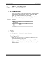
LPT1 parallel port ................................................................... 6-1
LPT1 parallel port ........................................................................................6-1
Printer ............................................................................................................ 6-1
Installing a printer .............................................................................. 6-1
Display ...........................................................................................................6-2
Installing a display .............................................................................. 6-2
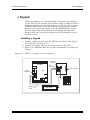
Keypad ...........................................................................................................6-3
Installing a keypad .............................................................................. 6-3
iv
PC-680 user’s manual
Contents
Chapter 7:
Console devices ....................................................................... 7-1
Description .................................................................................................... 7-1
Selecting console devices ............................................................................. 7-1
XVGA ..................................................................................................... 7-1
Serial console ........................................................................................ 7-1
Transferring files between the PC–680
and your PC ............................................................................................. 7-3
Transferring files to the PC–680 ................................................................. 7-4
Transferring files from the PC–680 ............................................................ 7-5
Example of downloading a file to the PC–680 ........................................... 7-6
Remote disks ................................................................................................. 7-8
Downloading files to the PC–680 using REMDISK/REMSERV ..... 7-8
Chapter 8:
SSDs, DRAM, and battery backup ....................................... 8-1
Description .................................................................................................... 8-1
SSD0 ............................................................................................................... 8-1
Battery backup for SSD0 SRAM and real time calendar clock ................ 8-2
SSD1 ............................................................................................................... 8-2
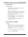
Managing SSDs ............................................................................................. 8-3
Flash file system .................................................................................. 8-3
Defining SSDs using SETSSD ..................................................................... 8-3
SETSSD ................................................................................................. 8-3
Using FXFMT to format an SSD ................................................................. 8-5
Formatting SSD1 .................................................................................. 8-5
Using SYS to make an SSD bootable ...........................................................8-5
Adding operating system startup files (using SYS) ......................... 8-5
Using SETSSD and TESTOEM to test an SSD .......................................... 8-6
Making copies of the PC–680 SSD .............................................................. 8-7
Programming copies of the PC–680 SSD .................................................... 8-7
Programming a new BIOS into SSD1 ......................................................... 8-8
DRAM ............................................................................................................. 8-8
Chapter 9:
External drives ........................................................................ 9-1
Description .................................................................................................... 9-1
Floppy disk controller .................................................................................. 9-1
Power requirements ............................................................................ 9-1
Installing a floppy disk drive .............................................................. 9-1
Hard disk controller .................................................................................... 9-1
Power requirements ............................................................................ 9-2
Installing an IDE drive: .......................................................................9-2
Chapter 10: Digital I/O ................................................................................ 10-1
Description .................................................................................................. 10-1
Major features ............................................................................................. 10-1
Software ....................................................................................................... 10-1
Jumpers and connectors ............................................................................ 10-2
Programmable registers ............................................................................. 10-3
Standard operating mode .......................................................................... 10-3
I/O port operation .............................................................................. 10-3
Event sense operation ....................................................................... 10-4
Mask register operation ................................................................... 10-4
Enhanced operating mode ......................................................................... 10-5
Register bank selection ............................................................ 10-5
v
Contents
PC-680 user’s manual
Bank 0 operations ...................................................................................... 10-5
Digital I/O (I/O0–I/O31), registers 0–3, bank 0 (r/w) ....................... 10-5
Mask register: Register 7, bank 0 (r/w) ............................................ 10-6
External event sense register: Register 6, bank 0 (r/w) ................. 10-7
Bank 1 operations ....................................................................................... 10-7
Event sense registers: Registers 0–3, bank 1 (r/w) ......................... 10-7
Event control register 0: Register 6, bank 1 (w) ............................. 10-8
Event status register 0: Register 6, bank 1 (r) ................................ 10-8
Event control register 1: Register 7, bank 1 (w) ............................. 10-9
Bank 2 operations ..................................................................................... 10-10
Debounce control register: Register 0, bank 2 (r/w) ..................... 10-10
Debounce duration register 0: Register 1, bank 2 ......................... 10-11
Debounce duration register 1: Register 2, bank 2 ......................... 10-12
Bank select register 2: Register 7, bank 2 (r/w) ............................ 10-13
Octagon operating mode .......................................................................... 10-13
Advanced control register 0 (Address offset: 10h) ........................ 10-13
Delta sense register (0–5): (Address offset: 12h–17h) ................ 10-14
Polarity event extended registers (0–5):
(Address offset 10h–1Dh) .......................................................... 10-14
Chapter 11: CRTs and flat panels ............................................................ 11-1
Description .................................................................................................. 11-1
Video features ............................................................................................. 11-1
Programming the video BIOS .................................................................... 11-2
Connecting a monitor ................................................................................. 11-3
Analog monitor ................................................................................... 11-4
Connecting a flat panel display ................................................................. 11-4
Flat panels requiring bias voltage .................................................... 11-5
LCD bias control example ........................................................ 11-5
Connecting the flat panel to the PC–680 ......................................... 11-6
Chapter 12: PC/104 expansion .................................................................. 12-1
Description .................................................................................................. 12-1
Chapter 13: Ethernet ................................................................................... 13-1
Description .................................................................................................. 13-1
Ethernet drivers ................................................................................ 13-1
Chapter 14: USB ........................................................................................... 14-1
Description .................................................................................................. 14-1
Chapter 15: Watchdog timer and hardware reset ............................... 15-1
Description .................................................................................................. 15-1
Enhanced INT 17h function definitions ................................................... 15-1
Enable watchdog ................................................................................ 15-1
Strobe watchdog ................................................................................. 15-3
Disable watchdog ............................................................................... 15-3
Hardware reset ........................................................................................... 15-4
Overview: Section 3 – System management
Chapter 16: Serial EEPROM and CMOS RAM ...................................... 16-1
Description .................................................................................................. 16-1
Enhanced INT 17h function definitions ................................................... 16-1
vi
PC-680 user’s manual
Contents
Serial EEPROM .......................................................................................... 16-1
Read a single word from the serial EEPROM ................................ 16-1
Write a single word to the serial EEPROM .................................... 16-2
Read multiple words from the serial EEPROM ............................. 16-3
Write multiple words to the serial EEPROM ................................ 16-3
Return serial EEPROM size ............................................................. 16-4
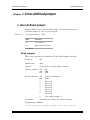
Chapter 17: User-defined jumper ............................................................ 17-1
User-defined jumper ................................................................................... 17-1
Read jumpers ...................................................................................... 17-1
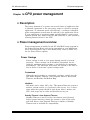
Chapter 18: CPU power management ..................................................... 18-1
Description .................................................................................................. 18-1
Power management overview .................................................................... 18-1
Power Savings ..................................................................................... 18-1
Customized ................................................................................ 18-1
Maximum Power Savings.......................................................... 18-2
Maximum Performance ............................................................. 18-2
Thermal management ........................................................................ 18-2
Thermal Setpoint ...................................................................... 18-2
Thermal Hysterises ................................................................... 18-2
Fan Control ................................................................................ 18-3
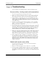
Chapter 19: Troubleshooting .................................................................... 19-1
No screen activity – checking console serial communications ...... 19-1
Garbled serial console screen activity ............................................. 19-1
System generates a BIOS message but locks up when booting from
SSD1 .............................................................................................. 19-2
Flash file reports a drive, but issuing a DIR generates an error
message ......................................................................................... 19-2
Flash file does not report the drive ................................................. 19-2
System will not recognize hard drive .............................................. 19-2
System locks up after powerdown/powerup ................................... 19-3
Technical assistance ................................................................................... 19-3
POST Codes ................................................................................................. 19-4
Overview: Section 4 – Appendices
Appendix A: Technical data .......................................................................... A-1
Technical specifications .............................................................................. A-1
CPU .............................................................................................. A-1
PCI bus speed ............................................................................ A-1
ISA bus speed ............................................................................ A-1
SDRAM ........................................................................................ A-1
SSD0 ............................................................................................ A-1
SSD1 ............................................................................................ A-1
SSD2 ............................................................................................ A-1
Floppy drive ................................................................................ A-1
EIDE drives ................................................................................ A-1
Video ............................................................................................ A-2
10/100Base–T Ethernet port ..................................................... A-2
Serial I/O ..................................................................................... A-2
Parallel port ................................................................................ A-2
vii
Contents
PC-680 user’s manual
Digital I/O ................................................................................... A-2
USB .............................................................................................. A-3
Speaker ........................................................................................ A-3
Keyboard, mouse port ................................................................ A-3
PC/104 interface ......................................................................... A-3
Battery backup ........................................................................... A-3
Watchdog timer .......................................................................... A-3
Bus mastering ............................................................................. A-3
BIOS ............................................................................................ A-3
ROM–DOS ................................................................................... A-3
Power requirements ................................................................... A-3
Voltage supervisor ..................................................................... A-4
Environmental specifications ................................................... A-4
Size ............................................................................................... A-4
Connectors .................................................................................................. A-10
Connector pinouts ...................................................................................... A-11
Appendix B: Software utilities ................................................................... B-1
Introduction .................................................................................................. B-1
Support commands and device drivers:............................................ B-1
GETBIOS.EXE ............................................................................................. B-2
GETIMG.EXE ............................................................................................... B-2
GETIMGH.EXE ........................................................................................... B-3
I17HNDLR.EXE ........................................................................................... B-4
LCDBIAS.EXE ............................................................................................. B-5
LPT1CON.COM ............................................................................................ B-6
FXFMT.EXE ................................................................................................. B-7
FXDOS.SYS .................................................................................................. B-7
PGMBIOS.EXE ............................................................................................ B-8
PGMIMG.EXE .............................................................................................. B-9
PGMIMGH.EXE ......................................................................................... B-10
REMDISK.EXE .......................................................................................... B-11
REMQUIT.COM ......................................................................................... B-13
REMSERV.EXE .......................................................................................... B-14
RESET.COM ............................................................................................... B-15
SETSSD.EXE .............................................................................................. B-16
TESTOEM.EXE ......................................................................................... B-17
TRANSFER.EXE........................................................................................ B-18
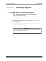
Appendix C: Third party support .............................................................. C-1
Using M–Systems DiskOnChip (DOC) ...................................................... C-1
Appendix D: Accessories .............................................................................. D-1
Appendix E: Operation in severe environments ................................... D-1
Operation under high / continuous vibration .................................. D-1
Operation at high temperatures ....................................................... D-1
Warranty
Limitations on warranty ........................................................................ 1
Service policy ........................................................................................... 1
Returning a product for repair .............................................................. 2
Returns ..................................................................................................... 2
Governing law ......................................................................................... 2
viii
PC-680 user’s manual
Contents
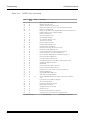
List of figures
Figure
Figure
Figure
Figure
Figure
Figure
Figure
Figure
Figure
Figure
Figure
Figure
Figure
Figure
Figure
Figure
Figure
2-1
2-2
2–3
2–4
5–1
5–2
5–3
6–1
6–2
7–1
7–2
7–3
11–1
11–2
11–3
12–1
B–1
PC-680 component diagram ................................................................... 2-5
PC-680 center-to-center mounting hole diagram ................................ 2-6
Power connector ...................................................................................... 2-7
Keyboard and monitor connections ...................................................... 2-8
Null modem adapter and VTC–20F cable ............................................. 5-9
PC-680 serial devices ............................................................................ 5-10
RS-422 and RS-485 hookup diagrams ................................................. 5-12
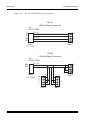
LPT1 as a printer port ............................................................................ 6-2
LPT1 as a display and/or keypad port .................................................. 6-3
The PC–680 and a serial console ...........................................................7-2
VTC–20F cable and null modem adapter ............................................. 7-3
Downloading files to the PC–680 using REMDISK/REMSERV ........ 7-8
The PC–680, a VGA monitor, and a PS–2 compatible keyboard ....... 11-2
The PC–680 and a VGA monitor .......................................................... 11-4
The PC–680 and a flat panel display ................................................... 11-6
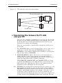
Typical PC/104 module stack ............................................................... 12-1
Cabling diagram for a standard cable ................................................ B-12
ix
Contents
PC-680 user’s manual
List of tables
Table 2–1
Table 2–2
Table 3–1
Table 3–2
Table 3–3
Table 3–4
Table 3–5
Table 3–6
Table 5–1
Table 5–2
Table 5–3
Table 5–4
Table 5–5
Table 5–6
Table 5–7
Table 5–8
Table 6–1
Table 8–1
Table 8–2
Table 10–1
Table 10–2
Table 10–3
Table 10–4
Table 10–5
Table 10–6
Table 10–7
Table 10–8
Table 10–9
Table 10–10
Table 10–11
Table 10–12
Table 10–13
Table 10–14
Table 10–15
Table 10–16
Table 10–17
Table 10–18
Table 10–19
Table 10–20
Table 10–21
Table 10–22
Table 10–23
Table 10–24
Table 10–25
Table 10–26
Table 13–1
Table 15–1
Table 15–2
x
PC–680 jumper configurations .............................................................. 2-2
PC–680 jumper configurations (continued) .......................................... 2-3
PC–680 BIOS setup parameters ............................................................ 3-2
PC–680 BIOS setup parameters (continued) ....................................... 3-3
PC–680 BIOS setup parameters (continued) ....................................... 3-4
PC–680 BIOS setup parameters (continued) ....................................... 3-5
PC–680 BIOS setup parameters (continued) ....................................... 3-6
PC–680 BIOS setup parameters (continued) ....................................... 3-6
COM port configurations .......................................................................5-2
COM1 and COM2 pinout (J7 connector) .............................................. 5-3
COM3 and COM4 pinout (J10 connector)............................................. 5-4
COM3 and COM4 jumper configurations ............................................. 5-5
COM5 and COM6 pinouts for RS-232 (connector J14) ........................ 5-7
COM5 and COM6 pinouts for GPS (connector J19) ............................5-7
Interrupt status register ........................................................................ 5-8
COM3, COM4 transmitter control ...................................................... 5-11
LPT port ................................................................................................. 6-1
SSD0 device selection jumpers: W20, W21 ............................................ 8-1
Battery connector: J13 ............................................................................8-2
Digital I/O port ...................................................................................... 10-1
W5: Pull–up and pull–down jumpers ................................................. 10-2
J6: Digital I/O [0:7], [8:15], [16:23], J5: Digital I/O [24:31] ................. 10-2
Standard I/O port addressing .............................................................. 10-3
I/O point write/read ports (port and I/O point assignments) ........... 10-3
Event sense register ............................................................................. 10-4
Event sense inputs ................................................................................ 10-4
Mask port ............................................................................................... 10-5
Register bank selection ........................................................................ 10-5
Digital I/O (I/O0–I/O31), registers 0–3, bank 0 (r/w) .......................... 10-6
Mask register......................................................................................... 10-6
Event sense status ................................................................................ 10-7
Example of event sense register ......................................................... 10-8
Event control register .......................................................................... 10-8
Event status register 0 ......................................................................... 10-9
Event control register 1 ....................................................................... 10-9
Bank select status register ................................................................ 10-10
Debounce control register .................................................................. 10-10
Debounce duration .............................................................................. 10-11
Debounce duration register 0 ............................................................ 10-11
Debounce duration register 1, port 2, bank 2 ................................... 10-12
Debounce duration register 1 ............................................................ 10-12
Bank select register 2 ......................................................................... 10-13
Advanced control register 0 ............................................................... 10-13
Delta sense registers (0–5) ................................................................. 10-14
Polarity event extended registers ..................................................... 10-15
Ethernet LEDs ...................................................................................... 13-1
W18 Power Fail Indicator jumper ....................................................... 15-1
BX register values ................................................................................ 15-2
PC-680 user’s manual
Table 18–1
Table 19–1
Table 19–2
Table 19–3
Table 19–4
Table A–1
Table A–2
Table A–3
Table A–4
Table A–5
Table A–6
Table A–7
Table A–8
Table A–9
Table A–10
Table A–11
Table A–12
Table A–13
Table A–14
Table A–15
Table A–16
Table A–17
Table A–18
Table A–19
Table A–20
Table A–21
Table A–22
Table A–23
Table A–24
Table A–25
Table A–26
Table A–27
Table D–1
Table D–2
Table D–3
Contents
PC-680 BIOS setup Power Screen options ......................................... 18-3
POST Codes ........................................................................................... 19-4
POST Codes (continued) ...................................................................... 19-5
POST Codes (continued) ...................................................................... 19-6
POST Codes (continued) ...................................................................... 19-7
PC–680 memory map ............................................................................. A-5
PC–680 I/O address map ....................................................................... A-5
PC–680 jumper configurations ............................................................. A-6
PC–680 jumper configurations (continued) ......................................... A-7
COM1 - COM6 serial ports ................................................................... A-8
LPT1 port ................................................................................................ A-9
Digital I/O port ....................................................................................... A-9
Connectors and mating recepticles .................................................... A-10
Fan: J1
.............................................................................................. A-11
Speaker: J2 ............................................................................................ A-11
Power: J3 .............................................................................................. A-11
Flat panel: J4 ........................................................................................ A-12
Digital I/O: J5, J6 .................................................................................. A-13
COM1 / COM2: J7 ................................................................................. A-13
PC video: J8 .......................................................................................... A-14
PC/104: J9 .............................................................................................. A-15
COM3 / COM4: J10 ............................................................................... A-16
Floppy port: J11 .................................................................................... A-17
SVGA CRT: J12 ..................................................................................... A-17
Battery: J13 ........................................................................................... A-18
COM5 / COM6: J14 ............................................................................... A-18
Ethernet: J15 ........................................................................................ A-18
USB: J16 .............................................................................................. A-19
LPT: J17 .............................................................................................. A-19
IDE hard drive: J18 .............................................................................. A-20
COM5 / COM6 - GPS: J19 .................................................................... A-21
Keyboard / Mouse: J20 ......................................................................... A-21
Cables and terminal board .................................................................... D-1
LCD displays and keypads .................................................................... D-1
Miscellaneous part numbers ................................................................. D-1
xi
PC–680 user’s manual
Overview:
Overview of Section 1
Section 1 – Installation
Section 1 provides installation and programming instructions, startup
options, and system configuration program examples. The following
chapters are included:
Chapter
Chapter
Chapter
Chapter
1:
2:
3:
4:
Overview
Quick start
SETUP programs
Save and run programs
PC–680 user’s manual
Chapter 1:
Overview
Overview
≡ Description
The PC–680 Mobile Industrial Computer™ (MIC) is a high performance, single board PC in Octagon’s product line. The PC–680 integrates serial communication, industrial digital I/O, floppy and PCI
bus hard disk ports, a multifunctional parallel port, and PCI bus
video that supports monitors and flat panels. This single–board
computer has two solid–state disks, a PC/104 interface, and a
10BaseT/100BaseTX Ethernet port.
The PC–680 is available with a 166 MHz Pentium CPU for –40 to +80C
operation or with a higher performance 266 MHz Pentium CPU. This
board is supplied with DOS 6.22 in ROM but will also execute other
operating systems such as LynxOS™, Windows 98™, Windows NT™,
Windows CE™, and QNX®. Since the PC–680 uses the same functional blocks as the Micro PC™, the circuitry has been fully proven as
reliable and the software is compatible with the software in the Micro
PC series.
≡ PC–680 major hardware features
CPU
Two versions are available - a 166 MHz or 266 MHz low-voltage
Pentium with MMX extensions. The PC–680 has a PCI bus speed of
33 MHz and an ISA bus speed of 8.33 MHz.
Up to 128 MB SDRAM
The PC–680 can hold up to 128 MB of SDRAM in a single SO–DIMM
socket. All DIMM modules from Octagon meet the full PC–680 temperature range.
Solid–state disks
Two solid state disks, SSD0 and SSD1, are present on the PC–680.
The flash file system allows both to be accessed as DOS compatible
drives. SSD0 is optionally installed by the user.
1–1
Overview
PC–680 user’s manual
SSD0
A 32–pin DIP socket accepts either an M–Systems DOC, 5V flash,
SRAM, or 512 KB/1 MB EPROM. The socket exhibits high retention
force and affords a gas tight contact. SSD0 is a user installed option.
SSD1
SSD1 contains the BIOS drive and ROM–DOS 6.22. Flash file system
software is included which allows the SSDs to emulate hard disk
operation.
Floppy and hard disk ports
The floppy disk port supports two standard floppy drives. The EIDE
hard drive port supports two EIDE devices including hard drives and
CD-ROM drive. The EIDE connector supplies +5V to a 2.5” hard
drive.
Boot sequence
A PC–680 can be configured to boot from the solid–state disk, an
external floppy, a hard disk, or CD.
Serial ports protected against ESD
The PC–680 has six serial ports with combinations of RS–232C,
RS–422, RS–485, and TTL (for GPS modules) interfaces. These serial
ports have the following common specifications:
IEC1000, level 3, ESD protection specification
— Contact discharge ±6 kV
— Air–gap discharge ±8 kV
Backdrive protection
16C550 compatible
Up to 115.2K baud
16–byte FIFO buffers
Enabled and disabled in BIOS SETUP
1–2
PC–680 user’s manual
Overview
Multifunctional printer port
The PC–680 incorporates the latest enhanced parallel port. It includes the following features:
Unidirectional
Bidirectional
IEEE 1284, ECP and EPP modes
14 mA of drive current
Backdrive protection
The following represent applications in the multifunctional parallel
port:
LPT1 for PC compatible printers
17 general purpose digital I/O lines
Up to a 4 x 4 matrix keypad
4–line alphanumeric display
Keypad and LCD display support for low cost operator
interface
For embedded applications, the parallel printer port can interface
with a 16–key matrix keypad and a 2– or 4–line LCD display. The PC–
680 is supplied with software that provides keypad scanning and
display operation. Supplied display and keypad drivers in C support
these devices.
32–bit digital I/O with versatile configuration
The PC–680 has 32 lines of industrial, digital I/O. Each I/O is a terminated, bidirectional line that can be individually configured as an
input, input with event edge sensing, input with level sensing, output, or output with readback. Inputs can generate interrupts or can
be polled. The lines are 5V compatible and can sink 25mA. The I/O
port can also drive the Octagon MPB series opto–isolation module
(Opto 22, G4 style) racks directly, controlling AC and DC loads to
240V at 3A.
Each line has a 4.7kW termination resistor, ESD, and
over/under shoot protection.
An interrupt can be generated from any of the 32 inputs. This interrupt can be enabled, disabled, and made to interrupt on a rising or
falling event/edge.
USB
The PC–680 contains two Universal Serial Bus (USB) ports.
1–3
Overview
PC–680 user’s manual
PCI bus XVGA, flat panel interface, and GUI accelerator
The video system on the PC–680 uses the advanced 69000 video
controller from Chips & Technologies. It supports CRT, LCD and EL
displays with resolutions to 1024 x 768 bpp x 16 (1280 x 1024 on some
selected displays). Displays from CGA through XVGA are supported.
The 69000 features a graphics accelerator with real time PC–video
being supported. Since the video circuitry operates on the PCI bus at
the full PCI bus speed, programs like Windows execute very rapidly.
The video section has 2 MB of video SDRAM for high–resolution
displays and simultaneous CRT and flat panel operation. The PC–680
supports 5V flat panel displays.
Adjustable display bias supply
An on–board voltage converter eliminates the need for a separate bias
supply for the LCD contrast control. The standard range for the bias
supply is from +23V to +29V.
Speaker, keyboard, and mouse ports
The speaker connector is PC compatible. The keyboard controller
accepts an AT style keyboard and has a PS–2 type connector. The
mouse port is combined with the keyboard port and is accessed with a
“y” cable. Neither the keyboard nor the mouse are required for operation.
PC/104 16–bit interface
The PC/104 interface accepts an 8– or 16–bit PC/104 expansion board.
PC/104 expansion boards are available from several manufacturers.
Ethernet
The PC–680 provides a 10BaseT/100BaseTX Ethernet port and supports the IEEE 802.3 Ethernet standard. The Ethernet controller IC
chip provides the following:
1–4
PCI interface
3 KB transmit buffer, 3 KB receive buffer
Integrated 10 BaseT/100BaseTX transceiver interface
Two LEDs for link and traffic status
Auto negotiating between full and half–duplex modes
Auto negotiating between 10Mbps and 100Mbps
PC–680 user’s manual
Overview
Watchdog timer added for safety
The watchdog timer resets the system or generates an NMI
(nonmaskable interrupt) if the program stops unexpectedly. The
watchdog is enabled, disabled and strobed under software control.
The time–out period is programmable from 0.5 to 60 seconds.
Hardware reset
A hardware reset ensures complete reset of the system and all attached peripherals. A hardware reset can be done by any of the following methods:
An expired watchdog timer cycle
Depressing the reset switch
Cycling power
Real time calendar/clock with battery–backup
The real time clock is fully AT compatible and uses the standard DOS
calls. An optional off–card battery powers the real time clock when
the 5 volt supply is removed.
5 Volt operation lowers system cost
The PC–680 operates from a single 5V ±5% supply.
5V ±5%, approximately 1.6 to 3.0A (dependent upon processor
type, speed and I/O devices), approximately 1A in standby
+12V and –12V supplied to PC/104 connector and display
connector; not required for PC–680 operation
Rugged environmental operation
Operating temperature
Nonoperating temperature
Relative humidity
Altitude
Shock
Vibration
–40° to 70°C, Intel Pentium
266 MHz with heatsink and
fan
–40° to 85°C, Intel Pentium
166 MHz
–55° to 90°C, nonoperating
5% to 95% noncondensing
–100 to 10,000 m
40g, 3 axis
6g, 3 axis
1–5
Overview
PC–680 user’s manual
Size
5.75” x 8.0”. Height is dependent on heatsink/fan selection
≡ PC–680 major software features
Advanced power management and system management
input
Power management can be used to reduce power consumption. This
reduces the heat load and extends the battery life in mobile applications.
Diagnostic software verifies system integrity automatically
The PC–680 has built–in diagnostic software that can be used to verify
on–card I/O and memory functions. On powerup or reset, a series of
tests are performed automatically. Memory verification does not
require software, test equipment, monitor, keyboard, disks, or test
fixtures.
BIOS SETUP information stored in EEPROM for high reliability
Loss of BIOS setup data is serious in industrial and mobile applications. Most PCs store the BIOS setup information in battery–backed
CMOS RAM. If the battery fails or is replaced during routine maintenance, this information is lost. Without a keyboard and monitor in
embedded applications, time consuming re–initialization is required.
The PC–680 stores the BIOS setup information in EEPROM with 512
bytes available to the user. Software routines to use this available
memory come with the PC–680.
Phoenix BIOS
The PC–680 has a Phoenix AT BIOS with power management and
Octagon BIOS extensions.
“Instant DOS” operating system
Datalight ROM–DOS v6.22 operating system is in flash. This means
that this version is always present on powerup. The system boots and
operates the same way as a desktop PC. Since all software and hard-
1–6
PC–680 user’s manual
Overview
ware are included, the system is fully operational “out of the box.”
Programmable video BIOS
The flash contains a video BIOS, which controls the on–board XVGA
controller. By default, the video BIOS supports a CRT only. To support flat panels, you can easily program in a new video BIOS.
On–board flash file system
The flash file system controls the on–board SSDs, which allows read/
write DOS access to the flash/SRAM. SSD0 can also use EEPROM.
For certain types of flash, the flash file system uses “wear leveling” to
spread the usage and maximize the lifetime of these devices.
Octagon BIOS extensions
On–board BIOS extensions allow easy access to digital I/O, serial
EEPROM, LCD bias control, watchdog timer functions, etc.
1–7
PC–680 user’s manual
Chapter 2:
Quick start
Quick start
This chapter covers the basics of setting up a PC–680 system and
tells you how to quickly install and power on the PC–680, and run a
demo program.
If you need to establish a serial console link instead of using the
monitor and keyboard, refer to the Serial console section in the
Console devices chapter.
WARNING!
The PC–680 Mobile Industrial Computer contains static sensitive
CMOS components. Do the following to avoid damaging your card
and its components:
Ground yourself before handling the PC–680 card
Disconnect power before removing or inserting a PC/104
expansion board
When programming a memory device, place the device in
the socket before applying power.
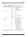
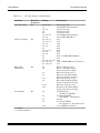
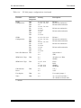
≡ Configuration Jumpers
Before you continue with the installation of your PC–680, review the
jumper configurations in Tables 2–1, 2–2, and the PC–680 diagram in
Figure 2–1 to become familiar with the jumper functions and locations.
2–1
Quick start
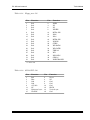
Table 2–1
PC–680 user’s manual
PC–680 jumper configurations
!"#$&&''
!"#$&&''
!"#*!+=''
?
@
Z\
Z\
Z\
Z\
Z\
Z\^_
Z\^_
Z\^_
`?
`?
`_?
`^?
`\?
`Z?
`?
`?
`?!"#*!+={''
`?
`_?
`^?!"#$&&''
`\?
+@
$|
}&
&
~_Z?'
~_Z&+
&&_Z
~\?'
~\&+
&&\
~?'
~&+
&^&
~?'
~&+
&\&
^
Z^
_
\_
|&
Z
Z\
^_
'
''
&&
2–2
~~$|
&+'+_
{&~$|
&&
'
&
~$|
&'&
{}&'
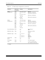
PC–680 user’s manual
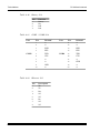
Table 2–2
Quick start
PC–680 jumper configurations (continued)
|!
&@
&
\
\
Z\^_
Z^\_
Z^\_
Z^\_
Z^\_
'
&
&
&
&
_
_
_
Z\^_
Z^\_
Z^\_
Z^\_
Z^\_
'
&
&
&
&
$&
\
'
!$
+_+}
_
*
*!'
+_+}
Z^_
Z
\_
^_
+|
*!'
{{|!
*&&&
?'
?
|&
&'
?
&&
'
&
|!
&@
&
\&
&
\&
&
\&
&
\&
&
'
2–3
Quick start
PC–680 user’s manual
≡ Installing the PC–680
Installation
To install the PC–680 you will need the following equipment
(or equivalent):
PC–680 Mobile Industrial Computer
+5V power supply - see Power Supply Requirements section
AT compatible keyboard with PS/2 connector
VGA monitor
VGA–12 cable (p/n #4565)
Hardware components required to mount the PC–680 (not included):
8 threaded hex stainless steel standoffs (4–40 x 3/8")
8 screws (4–40 x 1/4")
8 internal star lock washers (#4)
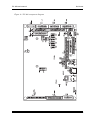
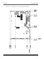
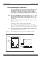
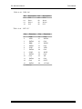
Refer to the PC–680 component diagram, Figure 2–1, for the location
of various connectors, and to the mounting hole diagram, Figure 2–2,
for installing your PC–680 system.
Speaker
If required, you can interface a speaker via a 4–pin connector at J2.
You may use any external speaker from 8–50 ohms. Refer to figure 2–
1 for the location of J2.
Keyboard and mouse
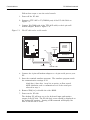
The PC-680 accepts an AT style keyboard and has a PS/2 type connector, located at J20. The mouse port shares the keyboard connector.
To use a keyboard, plug the keyboard directly into J20.
To connect a mouse, use a laptop style “y” cable, available at computer
stores, that which splits the J20 signals into keyboard and mouse
connectors.
Note
2–4
See Appendix A - Connectors for mating information.
PC–680 user’s manual
Quick start
Figure 2-1 PC-680 component diagram
2–5
Quick start
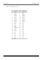
Figure 2-2
2–6
PC–680 user’s manual
PC-680 center-to-center mounting hole diagram
PC–680 user’s manual
Quick start
1. Use the standoffs, washers, and screws and place them in the eight
holes on the PC–680 board. Refer to Figure 2–2 for the center–to–
center mounting hole dimensions and for the location of the designated holes used for mounting the hardware.
WARNING!
All eight standoffs, screws and washers must be used to secure the
PC–680. The standoffs will ensure full support not only on all four
sides, but also in the middle of the board. This will reduce circuit
board flex when a PC/104 expansion board or SSD0 device is
inserted.
In high vibration and shock environments, the standoffs are required to avoid damage to the electronic components and circuit
board traces.
2. Connect a 5V power source to the PC–680. Refer to the Power Supply
Requirements section. If you are using a PC/104 expansion card, you
may also require a ±12V source.
The power supply connector is located at J3. Refer to Figure 2–3.
Make certain to use both +5V connections and both ground connections. This is required for proper operation.
WARNING!
Accidently crossing the wires, i.e., plugging +5V wires into the
ground connector or the ground wires into the +5V connector will
damage the PC–680.
Figure 2–3
Power connector
Note
Gnd
+5V
+12V
–12V
+5V
Gnd
J3
Power header
See Appendix A - Connectors for mating information.
2–7
Quick start
PC–680 user’s manual
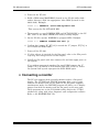
3. Connect the PS–2 style keyboard directly to the keyboard port at J20
and a VGA monitor to J12 using a VGA–12 cable. Refer to Figure 2–4.
Figure 2–4
Keyboard and monitor connections
VGA-12
cable
PC-680
Keyboard
cable
VGA Monitor
≡ PC–680 power supply requirements
The PC–680 is designed to operate from a single +5 VDC supply,
connected at J3. The typical current requirements for the PC–680 is
listed in the Technical data appendix. If you are using the PC/104
interface, you may also require ±12 VDC. Make sure that you utilize
both +5 VDC conductors and both ground conductors.
The user should also consider other factors such as the power cable
conductor gauge, number and length of conductors, mating connectors, and the power supply to external devices such as hard drives,
floppy drives, displays, mouse, and keyboard.
It is important that a quality power supply be used with the PC–680
that has sufficient current capacity, line and load regulation, hold up
time, current limiting, and minimum ripple.
The power supply for the PC–680 must meet the startup risetime
requirements specified in the ATX Power Design Guide, version 1.1,
section 3.3.5. This ensures that all the circuitry on the PC-680 sequences properly and avoids system lockup.
2–8
PC–680 user’s manual
Quick start
Also, select a power supply that discharges quickly. If large power
supply output capacitors are used, powering the system down and
then up may lock up the PC–680. If the power supply does not drain
below 0.7V, the CMOS components on the PC–680 will act like diodes
and forward bias, potentially damaging the PC–680 circuitry.
The proper selection of a quality power supply ensures reliability and
proper functioning of the PC–680.
WARNING!
Make sure the power supply is OFF when connecting the power
cable to the PC–680 board. Damage to the PC–680 may occur if the
power is ON when connecting the power cable.
≡ Running a demo program
Logon message
1. Power on the PC–680.
2. A logon message similar to the one below appears on your PC
monitor:
PhoenixBIOS 4.0 Release 6.0
Copyright 1985-1998 Phoenix Technologies Ltd.
All Rights Reserved
Octagon Release: VX.14B-2/3/00
Build Time: 10/13/99 10:37:31
CPU = Pentium(R)MMX(TM) 166 MHz
640K System RAM Passed
64512K Extended RAM Passed
0512K Cache SRAM Passed
System BIOS shadowed
Video BIOS shadowed
UMB upper limit segment address: E8B8
Press <F2> to enter BIOS setup
PC-680 INT 17h BIOS extension v1.15 Copyright © 19952000, Octagon Systems
FlashFX 4.01.153 (386 DOS)
Copyright © 1993-1998, Datalight Inc.
Datalight Patent Pending
Octagon Systems V2.01 – PC-680
SETSSD SSD1 /BEFORE
4Mb Strata Flash detected in SSD1
2–9
Quick start
PC–680 user’s manual
Starting ROM–DOS...
PC680 C:\> demo
Then a demonstration program will begin.
Press any key to continue
3. Use the directory command to make sure your equipment and software are working properly. Enter:
PC680 C:\> DIR
A similar directory listing of files stored in the SSD1 device should be
displayed:
Volume in drive C is SSD1
Volume Serial Number is 3214–1BE4
Directory of C:\
COMMAND
AUTOEXEC
CONFIG
DOS
UTILS
DEMO.EXE
DEMO
COM
26,321
BAT
38
SYS
67
<DIR>
<DIR>
EXE
27,922
BAS
5,045
7 file(s)
04–12–96
6:22p
04–12–96
8:26p
04–12–96
8:26p
04–12–96
8:26p
04–12–96
8:26p
04–12–96
8:26p
04–12–96
8:26p
26,426 bytes
105,472 bytes free
If you do not get the proper logon message, please do the following:
Make sure all jumpers are set to factory defaults. Refer to Tables
2–1 and 2–2 for the default jumper settings.
If the system still does not respond, remove W26[3–4] to use the
default BIOS setup and try again. Also, refer to the Troubleshooting chapter.
2–10
PC–680 user’s manual
Quick start
≡ What’s next
1. To run BIOS setup and configure the system, see the BIOS setup
chapter.
2. To connect a floppy and/or hard drive, see the External drives chapter.
3. To use a serial console, refer to the Console devices chapter.
4. To transfer files from a host PC and/or to use a remote disk via a
serial connection, refer to the Console devices chapter
2–11
PC–680 user’s manual
Chapter 3:
SETUP programs
BIOS setup
≡ Introduction
Two system configuration programs exist for the PC–680. They are:
BIOS setup — Configures devices set up by the BIOS such as
serial ports, floppy drives, power management, etc.
SETSSD.EXE — Configures boot order for the SSD devices. For
information on SETSSD.EXE, refer to the Managing SSDs section
in the SSDs, DRAM, and battery backup chapter.
≡ BIOS setup
The BIOS is shipped with default configuration parameters stored in
the serial EEPROM. BIOS setup defines the PC–680 system parameters. System parameter changes are made by entering the BIOS
setup program.
BIOS setup is entered by pressing the F2 key during BIOS POST
sequence (this occurs between the memory test and boot).
Refer to Tables 3–1, 3–2, 3–3, 3–4, 3–5, and 3–6 for a list of setup
options.
Running BIOS setup
1. To run BIOS setup make sure you have installed a keyboard and
monitor with the PC–680 or a establish a serial communications link
between the PC–680 and your PC. See the Console devices chapter for
more information on these two options.
2. During the BIOS POST sequence (this occurs between the memory
test and boot) press the F2 key .
Press <F2> to enter SETUP
3–1
SETUP programs
Table 3–1
PC–680 user’s manual
PC–680 BIOS setup parameters
@
+*
@
+~
+
'~
_=~
`!~
Z_=~
``!~'*&
`\\!~
!
}&
*'
&
+|!
}
*
~$|
+
'
{&
&
"
_
_
&+|!
!}
&
+
'
\
~*!&
+
'
{&
~$|
+
'
{&
}
&!
&
'
$|
$|
$|
$|
$|+!*
$|+!*
+!*!
+
'
!_!!!!
!
{&
'
+
~$|
{&
'
+
?~$|
{&
+
'
~!
+
'
{&
&
+
'
{&
{&
+_
&
+
'
{&
'
3–2
PC–680 user’s manual
Table 3–2
SETUP programs
PC–680 BIOS setup parameters (continued)
~$+{
{&
'
+
&
{&
'
+
~
$|
'
&
!
*+'
+
{&
*'
+
{&
!
~&
'
{
{
|&
~
$|
Z\'Z\~
*
{&
'
*
+
~
$|
\'\{\{\
$&
$'$
~
{&
'
*
+
~
$|
\'{\{\\
$&
$'$
{&
'
*
+
$Z'$
$&
&$^$_'$
+
{&
'
*
+
$&
&$^$_'$
{
{&
'
*
+
$&
&$^$_$'
{&
'
*
+
$&
&$^$_$'
'
3–3
SETUP programs
Table 3–3
PC–680 user’s manual
PC–680 BIOS setup parameters (continued)
+@
$|
{&
'
+
~
$|
___'
{&$
*'
Z^_
+
$&@
&
$*@
&
'
$$*!~@&{&
\__~
__
*
'
*
'
+___+
*
'
+__+Z
*
'
+\__+~
*
'
+__+
*
'
$$*${&
$
*
'
$
*
'
$
*
'
$Z
*
'
$^
*
'
$_
*
'
$
*
'
$
*
'
?
+
'
{&
~
^__^`=\`='Z`==
$&
|
|
&^
@+*!
|
+|'
&@
&+
'
&@
&
'
'
3–4
PC–680 user’s manual
Table 3–4
SETUP programs
PC–680 BIOS setup parameters (continued)
"
&@
+
'
#
!
&@
!
&
{&
#
$!
|'
|&
&}
|'
!&`!&`!&`!&`
\!&`!&`!&`
*&}
|'
!&`_!&`!&`
_!&`_!&`_!&`
_!&`
"
+}
+
'
_``_``
!&`!&`!&`!&`
\!&`_!&`!&`
|&!&@
|'
|&
{&
!
&@
|'
|&
{&
!
&
|
|&'
{&
}
&
_
"&
_
}
+
`Z`_'
`Z\Z`
&&
+
'
{&
@!
+
'
{&
@+
\`_`'`_``_``_`
'
3–5
SETUP programs
Table 3–5
PC–680 user’s manual
PC–680 BIOS setup parameters (continued)
+
@
+
"
+
~
*&
*}*$+|!+
~
Table 3–6
PC–680 BIOS setup parameters (continued)
#$
{|&
{
&@
&@
{+
&@
&@
+
+
&@
&@
3–6
PC–680 user’s manual
Chapter 4:
Save and run programs
Save and run programs
≡ Save and run your programs on the PC–680
Once you have written, tested and debugged your application, you can
then save it to flash memory in SSD1 or SSD0 (if you have flash, DOC,
or SRAM installed). When you reboot the PC–680, your program can
automatically execute. As shipped from the factory, SSD1 already
contains a bootable ROM–DOS.
This chapter describes the following:
Saving an application program to SSD1
Autoexecuting the program from the PC–680
Overriding autoexecution of your program
The information in this chapter assumes you are using ROM–DOS in
your application. Some Microsoft programs make undocumented DOS
calls. With ROM–DOS, an error returns when an undocumented DOS
call is made, causing your program to operate erratically. We recommend booting from SSD0 using your own DOS, when using programs
with undocumented DOS calls.
≡ Saving programs and support files
By default, the drive in SSD1 comes preformatted from the factory,
loaded with ROM–DOS, startup files and an example demo program.
To replace the demo program on SSD1 with your own, see the section
Adding your application, in this chapter. To reformat an SSD or to
add your own operating system, please refer to the SSDs, DRAM, and
battery backup chapter.
WARNING!
Reformatting SSD1 requires the use of a floppy or a hard disk to
restore system files.
4–1
Save and run programs
PC–680 user’s manual
Adding your application
To add your application to your SSD, do the following:
1. Three methods of copying your application to the SSD are available.
Do one of the following:
From a local drive on the PC–680, such as A: or C:, use the COPY
command to copy your application program to the SSD.
From a host PC using a terminal emulator, serially download your
application program by using the TRANSFER command. Refer to
the SSDs, DRAM, and battery backup chapter.
From a host PC, establish a remote drive and copy your application program from it, using the REMDISK and REMSERV commands. Refer to the SSDs, DRAM, and battery backup chapter.
2. Also copy any device drivers required for your application to the SSD.
CONFIG.SYS on the SSD may require modification to include the
device drivers.
3. To autoexecute your application, add your application name to the
AUTOEXEC.BAT file on the SSD. To replace the Octagon example
program (DEMO.EXE) with your application, substitute DEMO in the
AUTOEXEC.BAT file with your application program filename.
Note For information on CONFIG.SYS and AUTOEXEC.BAT, refer to your
DOS manual.
Autoexecuting your application from SSD1
1. SSD1 is the default boot device, drive C:. After adding your program
information to SSD1, including any required CONFIG.SYS files and
modifying AUTOEXEC.BAT to run your application file, reset the
system. Your application should begin execution.
Autoexecuting your application from SSD0
1. SSD0 first needs to be defined as the boot device, drive C:. After
adding your program information to SSD0, including any required
CONFIG.SYS files and modifying AUTOEXEC.BAT to run your
application file, use the SETSSD command to define SSD0 as the boot
device. Enter the following command:
PC680 C:\> SETSSD SSD0 SSD1 /before
2. Reset the system. SSD0 is now drive C: and your application should
begin execution.
Note
4–2
It is recommended that you leave SSD1 in the SETSSD options or
that you have a copy of SETSSD.EXE on SSD0. This allows you to
change your boot device back to SSD1 if needed.
PC–680 user’s manual
Save and run programs
Overriding the autoexecution of your application
You may stop the autoexecution of your application by performing
one of the following options:
Option 1
1. Press <Ctrl> C when the system boots to stop AUTOEXEC.BAT.
2. Change AUTOEXEC.BAT and/or CONFIG.SYS to not call out
your program.
Option 2
1. Install a floppy drive.
2. Change BIOS setup to enable the floppy drive and to boot from it.
Refer to the BIOS setup chapter.
3. Reset the system and boot from floppy using a bootable disk.
4. Change AUTOEXEC.BAT and/or CONFIG.SYS on C: to not call
out your program.
Option 3
1. Remove the “S” jumper, W7[9-10].
2. When prompted, press “1” for SSD1, then “O” for other, then “Y”
to save. then “Y” to abort CONFIG.SYS and AUTOEXEC.BAT.
3. Change AUTOEXEC.BAT and/or CONFIG.SYS to not call out
your program.
4–3
PC-680 user’s manual
Overview:
Overview of Section 2
Section 2 – Hardware
Section 2 discusses usage, functions, and system configurations of the
PC-680’s major hardware features. The following chapters are
included:
Chapter
Chapter
Chapter
Chapter
Chapter
Chapter
Chapter
Chapter
Chapter
Chapter
5:
6:
7:
8:
9:
10:
11:
12:
13:
14:
Serial ports
LPT1 parallel port
Console devices
SSDs, DRAM, and battery backup
External drives
Digital I/O
CRTs and flat panels
PC/104 expansion
USB
Ethernet
PC–680 user’s manual
Chapter 5:
Serial ports
Serial ports
≡ Description
The PC–680 has six serial ports, COM1 through COM6. These serial
ports interface to a printer, terminal, GPS (Global Positioning System) receiver, or other serial device. All ports support 5–, 6–, 7–, or 8–
bit word lengths, 1, 1.5, or 2 stop bits, and baud rates up to 115.2K.
COM1 and COM2 are dedicated 8–wire RS–232 ports. COM3 and
COM4 can be configured with jumpers to provide RS–232C, RS–422,
or RS–485. COM5 and COM6 provide 4–wire RS–232 or GPS and
RTCM SC–104 differential correction signal interfaces.
All serial ports have the following specifications:
16C550 compatible
16–byte FIFO buffers
IEC 1000, level 3, ESD protection
— Contact discharge ±6 kV
— Air–gap discharge ±8 kV
Backdrive protection
Up to 115.2K BPS operation
The following sections describe these ports in more detail.
5–1
Serial ports
PC–680 user’s manual
≡ Serial port configurations
Table 5–1 shows the configurations available for the COM ports.
Table 5–1
COM port configurations
%
&'
()*
+
%
|!
\&
@&
{\
\
{\
\'
$
$'
|!
\&
@&
{\
\'
{\
\
$'
$
|!
'
\
&
@&
{\
$^
$_'
$
&$
'
\
&
@&
{\
'
}}
&
@&
_
'
}!_
&
@&
|!
|!
|!
|!
|!
\
$^
$_'
$
&$
$^
$_
$'
&$
$^
$_
$'
&$
Z
Z
_
|!
_
|!
^}}
|!
^}!
|!
'
5–2
Note
Addresses and IRQs are selected in BIOS setup, port type is selected
by jumpers.
Note
IRQ9, 10, and 11 may be shared between COM3, COM4, COM5, and
COM6. The application software must be able to differentiate the
shared interrupt. Operating systems such as Windows NT configuration options for this.
PC–680 user’s manual
Serial ports
COM1 / COM 2
COM1 and COM2 are 8–wire RS–232 ports.
Table 5–2 shows the pinout for COM1 and COM2 on J7.
Table 5–2
COM1 and COM2 pinout (J7 connector)
|!
Note
;<=<%
++
++
+
+
+
+
}
}
}+
}+
}
}
Z
+}
Z
+}
\
$
\
$
^
+
^
+
_
_
|!
;<=<%
See Appendix A - Connectors for mating information.
COM3 / COM 4
COM3 and COM4 can each be configured as a 4–wire industrial RS–
232 interface, RS–422, or RS–485 interface. The IRQ for either port is
selected through BIOS setup.
COM3 and COM4 use the RTS pin to enable or disable the RS–485
transmit/receive function.
COM3 and COM4 may “share” an interrupt with COM5 and COM6.
The application software must be able to differentiate the shared
interrupt. Operating systems such as Windows NT configuration
options for this.
For more information, see the COM3 through COM6 interrupt/status
register section and COM3 / COM4 - RS-422 and RS-485 section in
this chapter.
Table 5–3 shows the pinout for COM3 and COM4 on J10.
5–3
Serial ports
PC–680 user’s manual
Table 5–4 shows the jumper selections for COM3 and COM4.
Table 5–3
COM3 and COM4 pinout (J10 connector)
%=
%>
Note
5–4
;<=<%
;><<
;>?@
}
+*}*
} +*}* +
}
}+
}
Z
\
^
+
+
+
_
}
+*}*
} +*}* +
}
}+
}
Z
\
^
+
+
+
_
See Appendix A - Connectors for mating information.
PC–680 user’s manual
Table 5–4
Serial ports
COM3 and COM4 jumper configurations
|!
&@
&
Z\^_'
&
&
Z^\_
__
&
&
Z^\_
\&
&
\
Z^\_
\_
&
&
\
Z^\_
_
Z\^_'
&
&
Z^\_
__
&
&
_
Z^\_
\&
&
Z^\_
\_
&
&
_
Z^\_
|!
&@
&
'
5–5
Serial ports
PC–680 user’s manual
COM5
COM5 can be used either as an industrial 4–wire RS–232 or as a
TTL Global Positioning System (GPS) module port. The IRQ is selected through BIOS setup.
For RS–232, COM5 and COM6 share J14. When used for GPS, the 10–
pin header at J19 is used for a TTL–level GPS module. The signals
are hardwired to both J14 and J19. If you connect an RTCM SC–104
differential correction data GPS module to J19, you cannot use J14 for
RS–232 on COM 5 or COM6. However, if you connect a GPS module
that does not use differential correction data, you can still use COM6
for RS–232.
For more information, see the COM3 through COM6 interrupt/status
register section in this chapter.
Table 5–5 shows the pinouts for COM5 and COM 6 on J14. Table 5–6
shows the pinouts for COM5 and COM6 on J19.
COM6
COM6 can be used either as an industrial 4–wire RS–232 or to route
the RTCM SC–104 differential correction data to the GPS receiver.
The IRQ is selected through BIOS setup.
For RS–232, COM5 and COM6 share J14. When used for GPS, the 10–
pin header at J19 is used for a TTL–level GPS module. The signals
are hardwired to both J14 and J19. If you connect an RTCM SC–104
differential correction data GPS module to J19, you cannot use J14 for
RS–232 for COM5 or COM6. However, if you connect a GPS module
that does not use differential correction data, you can still use COM6
for RS–232.
For more information, see the COM3 through COM6 interrupt/status
register section in this chapter.
Table 5–5 shows the pinouts for COM5 and COM6 on J14. Table 5–6
shows the pinouts for COM5 and COM6 on J19.
Note See Appendix A - Connectors for mating information.
5–6
PC–680 user’s manual
Table 5–5
Serial ports
COM5 and COM6 pinouts for RS-232 (connector J14)
%@
;<=<%
;<=<%
&
&
&
&
+
+
}
}
}+
}+
}
}
Z
&
Z
&
\
&
\
+
^
+
^
&
_
&
_
&
%J
Global Positioning System Interface
COM5 and COM6 provide 4–wire RS–232 or GPS and RTCM SC–104
differential correction signal interfaces. J19 provideds the TTL
signals necessary for a GPS receiver. Refer to table 5-10 for J19
pinouts.
Table 5–6
COM5 and COM6 pinouts for GPS (connector J19)
|!
}+}!_
|!
+}!_
|!
|!
|!
&
Z
+}
+
\
&
}
^
&
}+
_
*&&&
'
|!
* The jumper at W24 selects the voltage for a GPS antenna. For a 5V
antenna, position the jumper across pins 1-2 (default). For a 12V
antenna, position the jumper across pins 2-4. For a passive antenna,
leave W24 jumper off or on one pin only.
5–7
Serial ports
PC–680 user’s manual
COM3 through COM6 interrupt/status register
COM3 through COM6 share the same interrupts—IRQ9, IRQ10,
IRQ11, or no IRQ. The interrupts for these ports are specified in the
BIOS setup menu. You can use the same interrupt for COM3 through
COM6, or specify separate interrupts.
To determine which serial port caused the interrupt, read the interrupt status register from within your interrupt handler. Bit 3
through bit 6 show which serial port caused the interrupt.
Table 5–7
Note
5–8
Interrupt status register
KV X
|!
{\
_
_
|!&&&@
|!
{\
_
|!&&&@
|!
_
_
|!&&&@
|!
\
_
|!&&&@
All 0s indicate that there are no interrupts pending.
PC–680 user’s manual
Serial ports
≡ Function and use of serial ports
COM1 as serial console device
Instead of using the on–board XVGA to connect a monitor, you can
use COM1 as a console device. See the Console devices chapter for
more information.
When interfacing the PC–680 to your desktop PC, you must use a
VTC-20F cable and a null modem adapter.
Figure 5–1
Null modem adapter and VTC–20F cable
RS–232 Null modem cable
P2
P1
Null Modem Adapter
P3
VTC-20F Cable
Mating cables
Use a VTC–20F or VTC–20M cable to connect the COM ports to
external serial equipment. The P2 and P3 connectors are DB–9 female
(VTC–20F) or DB–9 male (VTC–20M) connectors which plug directly
into a 9–pin PC serial cable.
COM1 through COM6 as RS–232 I/O
COM1 through COM6 can be used as RS–232 serial ports. COM1 and
COM2 support 8–wire configurations, while COM3 through COM6
are 4–wire only configurations. Use a VTC–20F or VTC–20M cable to
interface from the PC–680 to the serial device. Refer to Figure 5–2.
5–9
Serial ports
PC–680 user’s manual
Figure 5–2
PC-680 serial devices
Serial device
PC-680
Serial device
COM6
COM5
COM4
COM3
COM2
COM1
Serial device
Serial device
Serial device
Serial device
COM3 / COM4 - RS–422, and RS-485
COM3 and COM4 can be configured as RS–232 (default), 4–wire RS–
422, or 2–wire RS–485 interface. To change the default configuration
from RS–232 to an RS–422, or RS–485 interface, refer to Table 5–4 for
jumper settings.
RS-422
RS-422 is a point to point, full duplex system requiring 2 wire pairs.
Distances of up to 4000 feet between each node is allowed. The receiving device must be terminated. COM3 and COM4 an be unterminated
or terminated with a 100 Ω termination resistor.
Figure 5-4 shows a typical RS–422 connection.
RS-485
RS-485 is a multipoint, half duplex system requiring 1 wire pair. Up
to 32 nodes can be on the same bus. Distances of up to 4000 feet
between the first and final node is allowed. All nodes must be connected to the bus with a stub as short as possible. A terminating
resistor must be connected at each end of the system. Any node
located between the end points should not be terminated. COM3 and
COM4 configurations can be unterminated or terminated with a 120
Ω termination resistor.
5–10
PC–680 user’s manual
Serial ports
An application may implement a node as either the “host” node or as
a “remote” node in an RS–485 network. There can be as many as 32
nodes without any bus repeaters in the network. A “host” is referred
to as the node that initiates communication; while a “remote” is
referred to as a node that is addressed by the host.
In any given communication sequence in an RS–485 network, there
can only be one host. The host is responsible for initiating communication, maintaining network registration, and providing housekeeping tasks with other nodes. Remotes cannot initiate a communication.
They can only respond to messages that are addressed to them from
the host.
Figure 5–3 shows a typical RS–485 connection.
Transmitter Control
The transmitter for the RS-422 and RS-485 interfaces is controlled by
the COM3 or COM4 RTS signal. To turn the transmitter ON and OFF
through software control, toggle bit 1 of COM3 or COM4 base address
+ 4. Refer to table 5–8 for transmitter control.
Table 5–8
COM3, COM4 transmitter control
|!
{\
&
{\ |!
{\
{\ X
&|
_
&|
&|
_
&|
5–11
Serial ports
PC–680 user’s manual
Figure 5–3
RS-422 and RS-485 hookup diagrams
RS-422
4 Wire (Full Duplex) Transmission
J10
COM3 / (COM4)
TX+
TXRX+
RX-
Pin 1 / (11)
Pin 2 / (12)
R+
RT+
T-
Pin 7 / (17)
Pin 8 / (18)
Node 1
PC-680
Node 2
RS-485
2 Wire (Half Duplex) Transmission
J10
COM3 / (COM4)
DATA+
DATA-
Pin 1 / (11)
R+
RT+
T-
Pin 2 / (12)
Node 1
PC-680
Node 4
R+
RT+
T-
R+
RT+
T-
Node 2
5–12
Node 3
PC–680 user’s manual
Chapter 6:
LPT1 parallel port
LPT1 parallel port
≡ LPT1 parallel port
The LPT1 port has a 26–pin connector. It supports the unidirectional
standard mode, bidirectional mode, enhanced parallel port (EPP)
mode, and extended capabilities port (ECP) mode.
The LPT1 port supports a number of devices including a PC compatible printer, a multiline display, or a matrix keypad.
Table 6–1
LPT port
+&X
Z\
Z\'
Y
%
$
$Z'
~
'
≡ Printer
Note
See Appendix A - Connectors for mating information.
Installing a printer
1. Make sure that the LPT1 port is in standard or bidirectional mode.
This is accomplished in BIOS setup.
2. Connect an Octagon VTC–5/IBM cable (p/n 1237) from the LPT1 port
(J16) to the DB-25 connector of your printer cable. Or use an Octagon
PCA-36 cable (p/n 4808) and connect directly to a Centronics type
printer interface.
6–1
LPT1 parallel port
PC–680 user’s manual
Figure 6–1
LPT1 as a printer port
PC-680
LPT1
parallel port
VTC-5/IBM cable
Printer cable
≡ Display
The LPT1 port supports either a 4 x 20 or a 4 x 40 liquid crystal
display (LCD). To interface the displays to the PC–680, use the Octagon 2010 interface board. A CMA–26 cable is required to connect the
interface board to the PC–680. The program DISPLAY.EXE (found on
the PC–680 utility disk) provides an easy method to use the display.
Refer also to the 2010 product sheet for more information on the
interface board.
Installing a display
1. Connect a CMA–26 cable from the LPT1 port on the PC–680 (J16) to
J1 on the 2010. See Figure 6–2.
2. Connect the display cable to either the 14–pin or 16–pin header on
the 2010. The size of the display will determine which header to use.
3. Refer to the file DISPLAY.DOC for more information on initializing
and using the display.
6–2
PC–680 user’s manual
LPT1 parallel port
≡ Keypad
LPT1 also supports 4 x 4 matrix keypads. To interface the keypad to
the PC–680, use the Octagon 2010 interface board. A CMA–26 cable is
required to connect the interface board to the PC–680. The program
DISPLAY.EXE (found on the PC–680 utility disk) provides an easy
method to use the keypad. Refer to the file DISPLAY.DOC on the
PC–680 utility disk for information on initializing and using the
keypad. Also, refer to the 2010 product sheet for information on the
interface board.
Installing a keypad
1. Connect a CMA–26 cable from the LPT1 port on the PC–680 (J16) to
J1 on the 2010. See Figure 6–2.
2. Connect the keypad cable to the 10–pin header on the 2010.
3. Refer to the DISPLAY.DOC file for more information on reading the
keypad.
Figure 6–2
LPT1 as a display and/or keypad port
Keyboard
connector
PC-680
LCD
connectors
2010 Interface
J1
Power connector
LPT1
parallel port
4x4 Keypad
CMA-26
cable
LCD display
6–3
PC–680 user’s manual
Chapter 7:
Console devices
Console devices
≡ Description
The PC–680 has three options for console devices. You can use the
on–board video with a monitor and a keyboard as your console. You
can also use COM1 as the console or you can run the system without
a console device.
≡ Selecting console devices
The following represent the PC–680’s three options for console devices:
XVGA and a local keyboard. The XVGA supports CRT, LCD, and
EL displays.
Serial console from COM1. A serial cable/null modem adapter
plugged into a host PC running a terminal emulator provides both
input and output. The local keyboard also allows input but is not
required for operation.
No console device means no video output, either from the XVGA
monitor or the serial console. The local keyboard allows input.
XVGA
For correct usage of the CRT and flat panel, see the CRTs and flat
panels chapter.
Serial console
COM1 can serve as a console device, allowing you to use your desktop
PC to communicate with the PC-680. Refer to Figure 7-1 to connect a
desktop computer to the PC-680 as a console device. This connection
requires a VTC–20F cable (p/n 4866) and a null modem adapter (p/n
3186). It also requires a terminal emulator program such as Windows
HyperLink, ProComm, or an equivalent program.
7–1
Console devices
PC–680 user’s manual
Follow these steps to use the serial console:
1. Power off the PC–680.
2. Connect a VTC–20F to J7 (COM1/2 port) of the PC–680. Refer to
Figure 7–1.
3. Connect P2 (COM1 side of the VTC–20F cable) to the 9–pin null
modem adapter. Refer to Figure 7–2.
Figure 7–1
The PC–680 and a serial console
PC-680
Null modem
adapter
Terminal
Emulator
Software
P3
COM
Port
P1
Desktop PC
(COM2)
P2
(COM1)
VTC-20F cable
4. Connect the 9–pin null modem adapter to a 9–pin serial port on your
PC.
5. Start the terminal emulator program. The emulator program needs
the communication settings to be:
38400 bps, 8 data bits, 1 stop bit, no parity, no flow control,
ANSI emulation, and to communicate out of the serial port
selected in step 4.
6. Remove W26[3–4] to disable the video BIOS.
7. Power on the PC–680.
The desktop PC will now act as the keyboard input and monitor
output of the PC-680. The PC-680 boot screen should be displayed on
the desktop PC monitor. Issuing a DIR command will display the
files on the PC-680 C: drive.
7–2
PC–680 user’s manual
Figure 7–2
Console devices
VTC–20F cable and null modem adapter
RS–232 Null modem cable
P2
P1
Null Modem Adapter
P3
VTC-20F Cable
≡ Transferring files between the PC–680
and your PC
Once you have established communications between your PC and the
PC–680, you can serially download files to any read/write drive used
by the PC–680. You can also upload files from the PC–680 to your
desktop PC for editing and debugging.
There are two methods to download files through the serial port to
the PC–680:
1. The TRANSFER utility is used to download files, one at a time over a
serial port, to the PC–680 using the XMODEM protocol. Select
XMODEM in your terminal emulator when sending or receiving files.
(See the note below on XMODEM).
2. REMDISK/REMSERV utilities allow access to all of the files on a
remote disk drive. Once these programs are executed, single or
multiple files can then be transferred to and from the PC–680 over a
serial port using DOS COPY or XCOPY commands.
TRANSFER.EXE, REMDISK.EXE and REMSERV.EXE are located
on the PC–680 BIOS drive in the DOS directory, and on the PC–680
utility disk in the \DOS directory. Refer to the Software utilities
appendix for more information on these programs.
Note
XMODEM only transfers files in which the file size is exactly on a 128
byte boundary. If the file size does not fall exactly on the boundary,
XMODEM automatically rounds the file size up to the next 128 byte
boundary with padding characters. For example, a file with a size of
10,000 bytes, will be rounded up to 10,112 bytes, transferred, and
written with the new file size. In most cases, this is not a concern, but
in some instances the XMODEM padding causes problems. The pad-
7–3
Console devices
PC–680 user’s manual
ding problems become apparent when an application program is
expecting a specific file size or is expecting characters other than the
padding characters to be at the end of the file.
≡ Transferring files to the PC–680
In order to transfer files from your PC to a PC–680 drive using the
TRANSFER program, you must do one of the following:
Execute the TRANSFER program from both the PC–680 and from
your PC.
or
Execute the TRANSFER program from the PC-680, then initiate a
send file command from your terminal emulator.
The following steps only detail the procedure for transferring files
using TRANSFER on both systems. Refer to TRANSFER.EXE in the
Software utilities appendix for more information.
1. Refer to the Serial console section in this chapter for establishing a
serial console connection between the PC-680 and your desktop PC.
2. Execute the TRANSFER program from the PC–680 to receive a file
from your PC.
PC680 C:\> TRANSFER /COMx /R /V <drive>filename.ext
COMx specifies the serial port to use where x represents a
value from 1-4. The default is 1.
/R specifies to receive a file (default).
/V enables the display of “R” when a block is received, or “T”
when a block is transmitted. Do not use /V when COM1 is the
console device.
<drive> is the drive on the PC–680 where the file will be transferred to.
filename.ext is the name of the file on the PC–680 which you
are receiving from your PC.
3. Execute the TRANSFER program from your PC to send a file to the
PC-680. TRANSFER.EXE must reside on the host system and you
must run TRANSFER from DOS or a DOS shell.
Note
If using a DOS shell, the idle sensitivity property for the DOS shell
must be set to minimum.
C:\>
TRANSFER /COMx /S /V <drive>filename.ext
COMx specifies the serial port to use where x represents a
7–4
PC–680 user’s manual
Console devices
value from 1-4. The default is 1.
/S specifies to send a file.
/V enables the display of “R” when a block is received, or “T”
when a block is transmitted. Do not use /V when COM1 is the
console device.
<drive> is the drive on the desktop PC where the file will be
transferred from.
filename.ext is the name of the file on the PC–680 which you
are receiving from your PC.
Note
TRANSFER will time-out if the sending program has not been
started after approximately 40 seconds. It displays the following
message:
Failed to receive <drive>filename.ext
Deleting <drive>filename.ext
Also, you may speed up the transfer using the /Bnnnn switch to
increase the baud rate. Example: /B57600. When using the serial
console, do not use the /B option on the PC–680. Instead, change the
serial console baud rate in BIOS setup.
≡ Transferring files from the PC–680
In order to transfer files from the PC–680 to your PC drive, you must
do one of the following:
Execute the TRANSFER program from both the PC–680 and from
your PC.
or
Execute the TRANSFER program from the PC-680, then initiate a
receive file command from your terminal emulator.
The following steps only detail the procedure for transferring files
using TRANSFER on both systems. Refer to TRANSFER.EXE in the
Software utilities appendix for more information.
1. Refer to the Serial console section in this chapter for establishing a
serial console connection between the PC-680 and your desktop PC.
2. Execute the TRANSFER program from the PC–680 to send a file from
your PC.
PC680 C:\> TRANSFER /COMx /S /V <drive>filename.ext
COMx specifies the serial port to use where x represents a
value from 1-4. The default is 1.
7–5
Console devices
PC–680 user’s manual
/S specifies to send a file (default).
/V enables the display of “R” when a block is received, or “T”
when a block is transmitted. Do not use /V when COM1 is the
console device.
<drive> is the drive on the PC–680 where the file will be transferred from.
filename.ext is the name of the file on the PC–680 which you
are sending to your PC.
3. Execute the TRANSFER program from your PC to receive a file from
the PC-680. TRANSFER.EXE must reside on the host system and
you must run TRANSFER from DOS or a DOS shell.
C:\>
TRANSFER /COMx /R /V <drive>filename.ext
COMx specifies the serial port to use where x represents a
value from 1-4. The default is 1.
/R specifies to receive a file. This is the default.
/V enables the display of “R” when a block is received, or “T”
when a block is transmitted. Do not use /V when COM1 is the
console device.
<drive> is the drive on the desktop PC where the file will be
transferred to.
filename.ext is the name of the file on the PC which you
are sending from the PC-680.
Note
TRANSFER will time-out if the sending program has not been
started after approximately 40 seconds. It displays the following
message:
Failed to receive <drive>filename.ext
Deleting <drive>filename.ext
Also, you may speed up the transfer using the /Bnnnn switch to
increase the baud rate. Example: /B57600.
≡ Example of downloading a file to the PC–680
The following information on downloading files between the PC–680
and your PC uses the example program DEMO.EXE. This file is on
the PC–680 utility disk.
Hardware and software requirements:
Desktop PC, running a terminal emulator, connected by a VTC20F cable and a null modem adapter to COM1 of the PC–680.
7–6
PC–680 user’s manual
Console devices
The following steps only detail the procedure for transferring files
using TRANSFER on both systems. Refer to TRANSFER.EXE in the
Software utilities appendix for more information.
1. Refer to the Serial console section in this chapter for establishing a
serial console connection between the PC-680 and your desktop PC.
2. Execute the TRANSFER program from the PC–680 to receive a file
from your PC.
PC680 C:\> TRANSFER DEMO.EXE
COM1 is the default serial port, receive is the default function, C:\ is
the default drive, DEMO.EXE is the file name to be received.
The following message is displayed from the PC–680:
Receiving DEMO.EXE . . .
3. Execute the TRANSFER program from your PC to send a file to the
PC-680:
Shell out to DOS from your terminal emulator program.
TRANSFER.EXE must reside on the host system.
C:\>
TRANSFER /S DEMO.EXE
COM1 is the default serial port, send is the selected function, C:\ is
the default drive, DEMO.EXE is the file name to be sent and resides
in the root directory of C:.
Note
TRANSFER.EXE will time-out if the sending program has not been
started after approximately 40 seconds. If the time-out occurs, the
following message from the PC–680 is displayed:
Failed to receive DEMO.EXE!
Deleting DEMO.EXE
4. When the file transfer is complete, exit the DOS shell back into the
terminal emulator.
5. Type the following DOS command to view the drive directory to
confirm that your file has been transferred to the PC–680:
PC680 C:\> DIR
The system will display the contents of PC-680 drive and will list the
DEMO.EXE file.
Volume in drive is <label>
Directory of <drive>:\
DEMO EXE
27264 01-07-00
2:57p
6. To execute the program you have just downloaded type:
PC680 C:\> DEMO
The DEMO program displays a message on your PC.
7–7
Console devices
PC–680 user’s manual
≡ Remote disks
Downloading files to the PC–680 using REMDISK/REMSERV
The following uses REMDISK/REMSERV with the PC–680.
Note
REMDISK.EXE, and REMSERV.EXE are DOS utilities and require
special considerations when executed in a Windows environment.
The Datalight web site, www.datalight.custhelp has information to
sucessfully implement REMDISK/REMSERV while in Windows.
Refer to the Software utilities appendix for more information on using
REMDISK.EXE and REMSERV.EXE
Hardware and software requirements:
A Desktop PC, using COM1 to communicated to the PC-680, and
running REMSERV.
A PC–680 system with a keyboard, VGA monitor, VTC-20F cable and
null modem adapter, running REMDISK from COM1.
1. Connect the equipment and load the appropriate software on each
system as per the following diagram:
Figure 7–3
Downloading files to the PC–680 using REMDISK/REMSERV
REMDISK
VGA-12 video cable
PC-680
REMDISK
PCREMSERV
SmartLINK
Null modem
adapter
P3
COM
Port
P1
(COM2)
(COM1)
7–8
P2
VTC-20F cable
Desktop PC
PC–680 user’s manual
Console devices
2. On the PC–680 system, execute REMDISK.EXE by entering:
PC680 C:\> REMDISK
The following similar message is displayed on the PC–680 monitor:
Remote Disk v1.0
Copyright (c) 1990-1994 Datalight, Inc.
All rights reserved.
Installed as Drive F: /COM1 /B115+ /T3
Note
REMDISK assigns the remote drive as the last drive in the system. In
this case, drive F: was assigned.
3. Execute REMSERV.EXE on the desktop PC:
C:\> REMSERV C:
The following message is displayed on the PC:
REMSERV v1.0
Copyright (c) 1990-1994 Datalight, Inc.
All rights reserved.
Using COM1 at 115K+ baud. Accessing Drive C:
Time-out is 2 seconds
Press <Esc> to Exit.(There may be a delay before exit occurs)
4. Files are transferred to the PC–680 read/write drives by using the
DOS COPY and XCOPY commands. From the PC–680 system, enter:
PC680 C:\> COPY F:\PC680\DEMO.EXE
PC680 C:\> DIR
PC680 C:\> DEMO.EXE
Where F: is actually the C: drive on the host PC, and the DEMO.EXE
file resides in the \PC680 directory on the host C: drive of the host
PC.
The DEMO program displays a message on the PC–680 monitor.
5. When finished, on the PC–680 system, execute:
PC680 C:\> REMDISK /U
This unloads REMDISK from the desktop PC.
6. On the desktop PC, press <ESC> to exit REMSERV.
7–9
PC–680 user’s manual
Chapter 8:
SSDs, DRAM, and battery backup
SSDs, DRAM, and battery backup
≡ Description
The PC–680 supports two solid–state disks and an OEM option for a
third disk. SSD0 is a socket for an SRAM, flash, M–Systems DOC, or
EPROM device. SSD1 is a 4 MB flash soldered on–board (8 MB OEM
option). SSD2 is available as an 8MB OEM option.
≡ SSD0
SSD0 can be populated with a 128K or 512K SRAM, a 512K flash, M–
Systems DOC, or a 512K EPROM. The jumpers at W20 and W21 must
be set to match the type of device installed (see Table 8–1).
WARNING!
Alignment of an SRAM, flash, DOC, or EPROM device into
SSD0 is critical. Mis-alignment may destroy the device and
possibly damage the PC-680. Be certain to properly align
pin 1 of either the SRAM, flash, or EPROM device with pin 1
of SSD0.
Table 8–1
SSD0 device selection jumpers: W20, W21
+_+} _
*
*!'
+_+} Z^_
Z
\_
^_
*"
! +|
*!'
{|!
'
The SETSSD.EXE command is used to notify the BIOS that a new
drive has been installed, sets the boot order for the drives, and assigns a drive letter to the drives. See the Managing SSDs section in
this chapter.
Flash and SRAM devices must be formatted using the FXFMT.EXE
command. After the devices are formatted, reset the system. You are
now ready to copy files to the device in SSD0.
For further information on installing, formating and programming
SSD0 devices refer to the Managing SSDs section.
8–1
SSDs, DRAM, and battery backup
PC–680 user’s manual
≡ Battery backup for SSD0 SRAM and real time
calendar clock
If SRAM is used in SSD0, a 3.6V AT battery (p/n 3186) is required for
battery backup of the SRAM files. This battery also backs up the
CMOS real time clock. The PC–680 does not have a battery installed
when it is shipped. To install the battery:
1. Power off the PC–680.
2. Install the 3.6V AT clock battery at the J13 connector. Refer to the
component diagram in the Quick start chapter for the location of J13.
Table 8–2
Battery connector: J13
Note
~
=
&
&
SRAM contents can be affected by system noise. Therefore, the use of
SRAM is not recommended in electrically noisy environments, especially when systems are critical.
≡ SSD1
SSD1 is a 4MB flash (8MB OEM) soldered on–board. It contains the
BIOS and ROM–DOS 6.22, and is intended for storing application
programs to be executed on powerup. It is the default boot drive.
SSD1 can be accessed directly as a read/write DOS drive. While this
is convenient for product development, the flash has a limited number of writes allowed. Therefore, Octagon does not recommend SSD1
be used as a data logging device.
8–2
PC–680 user’s manual
SSDs, DRAM, and battery backup
≡ Managing SSDs
Flash file system
By default the flash file extended BIOS is loaded at system boot. A
message similar to the following is displayed on your screen as the
system boots each flash file drive found:
FlashFX 4.01.153 (386 DOS)
Copyright © 1993-1998, Datalight Inc.
The flash file extended BIOS allows the PC–680 to boot from the flash
file system on–board the PC–680. These drives are “simulated” hard
drives that look like a standard hard drive on a PC. In some instances
it will be necessary to disable the flash file extended BIOS. This is
done by removing the “X” W7[3-4] jumper.
Note
When installing Windows NT operating system, it is necessary to
disable the flash file system.
The flash file system includes an extended BIOS (FLASHFX.IMG), a
device driver (FLASHFX.SYS), a format utility (FXFMT.EXE), and a
test utility (TESTOEM.EXE).
Use the device driver FLASHFX.SYS to access SSDs when booting
from a floppy or hard drive, when the extended BIOS
(FLASHFX.IMG) is disabled.
≡ Defining SSDs using SETSSD
SETSSD
SETSSD.EXE allows the user to set or change the SSD drive order,
and therefore the boot device as well. Solid state drives are "simulated" hard drives. They can exist before or after any IDE drives and
can appear in any order. By setting the order, the SSDs may be
accessed as C:, D:, etc. Drive designators will change depending on
the SETSSD settings.
The following examples demonstrate how to define SSD drive order:
To set SSD0 first and SSD1 second, enter the following command:
PC-680 C:\> SETSSD SSD0 SSD1
In this example, SSD0 is C: and SSD1 is D:.
8–3
SSDs, DRAM, and battery backup
PC–680 user’s manual
To set SSD1 first and SSD0 second, enter the following command:
PC-680 C:\> SETSSD SSD1 SSD0
In this example, SSD1 is C: and SSD0 is D:.
To use only SSD1, enter the following command:
PC-680 C:\> SETSSD SSD1
In this example, SSD1 is C: and SSD0 will not be available.
If there are other hard drives on the system, add the /before option
to place the order of the SSDs before the hard drives, or add the
/after option to place the SSDs after the hard drives. For example,
To set SSD0 as C:, SSD1 as D:, and an IDE drive as E:, enter the
following command:
PC-680 C:\> SETSSD SSD0 SSD1 /before
To set the IDE drive as C:, SSD1 as D:, and SSD0 as E:, enter the
following command:
PC-680 C:\> SETSSD SSD1 SSD0 /after
Reset the PC-680 after running SETSSD for the new parameters to
take effect.
Note
The SETSSD parameters may be overridden by removing the “S”
W7[9-10] jumper and resetting the system.
Other drive letter designations may be added by device drivers (such
as VDISK.SYS), which are in the CONFIG.SYS file on the boot drive.
The boot drive is based upon the drive order set by the SETSSD
command and by the BIOS setup "boot sequence" option. If the boot
sequence is set to Removable, then Fixed Drives, the system will look
for a floppy diskette in drive A:. If a diskette is not installed, or a
floppy is not defined, the boot drive will be the first drive specified in
the SETSSD command.
8–4
PC–680 user’s manual
SSDs, DRAM, and battery backup
≡ Using FXFMT to format an SSD
Formatting SSD1
This section describes how to format SSD1.
Reformatting SSD1 requires the use of a floppy or a hard
disk to restore system files.
1. Define the SSD order with the SETSSD command. Since the command input varies depending upon the parameters you need to enter,
see the SETSSD command in the Software utilities appendix.
2. To begin formatting SSD1, execute FXFMT as follows:
PC-680 C:\> FXFMT 8n
where n is the hard drive sequence number. This number includes
IDE drives and SSDs.
For example, if you have 0 IDE drives and SETSSD shows:
[HDDs] SSD0 SSD1
then enter the following to format SSD0:
PC-680 C:\> FXFMT 80
On the other hand, if you have 1 IDE drive, enter:
PC-680 C:\> FXFMT 81
Note
If the drive had not been formatted previously, reset the system
before accessing the drive. This allows DOS to recognize the drive
and add a letter designation to it.
Note
FXFMT.EXE must be downloaded from the PC–680 utility disk. This
file is located in the \UTILS directory.
Note
FXFMT.EXE will not format IDE/ATA drives.
Note
The drive order affects the number entered at the FXFMT command.
≡ Using SYS to make an SSD bootable
Adding operating system startup files (using SYS)
To add the system files, issue the following operating systems command:
8–5
SSDs, DRAM, and battery backup
PC–680 user’s manual
C:\> SYS d:
where d: specifies the drive letter.
For example, if your system has 1 IDE drive, and SETSSD shows
“[HDDs] SSD0 SSD1,” then SSD1 should be drive E:. To SYS this
drive, use the “SYS d:” command.
Note
SYS.COM must be downloaded from the PC–680 utility disk. This file
is located in the \DOS directory.
Note
If you are adding the MS–DOS operating system to SSD1, you must
first boot from an MS–DOS bootable device (floppy or hard drive).
Note
If you are not booting from ROM–DOS, and wish to SYS ROM–DOS
back to the drive, the SYS command requires you to issue the following ROM–DOS commands: COMMAND.COM, ROM–DOS.SYS and
SYS.COM.
≡ Using SETSSD and TESTOEM to test an SSD
SETSSD, when used with no parameters, is used to determine the
order of the SSDs. TESTOEM is an SSD test used to excercise the
SSD by writing and reading data. Refer to the Software utilities
appendix for more information.
CAUTION
TESTOEM.EXE will destroy all drive data on the SSD except
the reserved BIOS area. A boot drive, i.e. floppy, will be
required to reformat the SSd.
To test SSD0 and SSD1 perform the following:
1. Run SETSSD.EXE to determine which socket to use with TESTOEM.
The socket (either 0 or 1) depends on the order of the SSDs. The first
SSDx listed is socket 0 (S0) and the second SSDx listed is socket 1
(S1). To configure the order of the SSDs, see the Defining SSDs using
SETSSD section in this chapter.
For example, running SETSSD with no parameters may give the
following output:
PC-680 C:\> SETSSD
[FDDs] SSD1 SSD0 [HDDs]
In the above example, SSD1 is the first SSD (S0), and SSD0 is the
second SSD (S1).
8–6
PC–680 user’s manual
SSDs, DRAM, and battery backup
2. Execute TESTOEM /Sn where n is the socket determined in step 1.
For SSD0 in the above example, enter:
PC-680 C:\> TESTOEM /S1 /E
For SSD1 in the above example, enter:
PC-680 C:\> TESTOEM /S0 /E
≡ Making copies of the PC–680 SSD
GETIMG.EXE is used to capture an image from an existing flash file
drive. This is used to program SSD drives onto target systems from a
development system. Refer to GETIMG.EXE in the Software utilities
appendix.
1. To make a copy of the PC–680 to a local file, enter:
PC-680 C:\> GETIMG SSD1 <filename>
2. To make a copy of the PC–680 SSD to a remote file:
a. Copy GETIMGH.EXE from the PC-680 Utility disk to the C:\ root
directory.
b. Establish serial communications between the PC–680 and the
desktop PC using a terminal emulator such as Windows
HyperTerminal. Refer to Console devices, Chapter 7.
c. On the PC–680 enter:
PC-680 C:\> GETIMG SSD1 <filename>/COM1
d. On the desktop PC, exit the terminal emulator, and if running
Windows, exit Windows and restart in DOS mode. Enter:
C:\> GETIMGH <filename>/COM1
e. This will write the SSD image, <filename>, to the host drive.
≡ Programming copies of the PC–680 SSD
PGMIMG.EXE is used to program an image from an existing flash file
drive to other SSDs on target systems. It can be run locally from a
PC-680 to program an on-board SSD, or it can be run remotely from a
host PC to program an SSD on a target system. Refer to
PGMIMG.EXE in the Software utilities appendix.
1. Run GETIMG.EXE to make a copy of the PC–680 SSD to a local file or
GETIMGH.EXE to make a copy of the PC–680 SSD to a remote file.
Refer to the above section, Making copies of the PC–680 SSD.
8–7
SSDs, DRAM, and battery backup
PC–680 user’s manual
2. To program a disk image of a local file onto SSD1, enter:
PC-680 C:\>
PGMIMGH SSD1 <filename>
3. To program a copy of the PC–680 image to a target system SSD1 from
a host system:
a. Copy PGMIMGH.EXE from the PC-680 Utility disk to the C:\ root
directory.
b. Establish serial communications between the PC–680 and the
desktop PC using a terminal emulator such as Windows
HyperTerminal. Refer to Console Devices, Chapter 7.
c. On the PC–680 enter:
PC-680 C:\> PGMIMGH SSD1 <filename>/COM1
d. On the desktop PC, exit the terminal emulator, and if running
Windows, exit Windows and restart in DOS mode. Enter:
C:\> PGMIMGH SSD1 <filename>/COM1
e. This will write the image, <filename>, to the PC-680 target system
SSD drive.
≡ Programming a new BIOS into SSD1
To program a new BIOS into SSD1, issue one of the following
commands:
PC-680 C:\> PGMBIOS filename SSD1
or
PC-680 C:\> PGMBIOS SSD0 SSD1
Note
You may need to use the /P option when issuing the PGMBIOS command if the “B” W7[1-2] jumper, and the “P” W7[7-8] jumpers are set
to boot from the SSD being programmed.
≡ DRAM
The PC–680 is shipped with 0 MB of DRAM. The on–card memory
socket accepts 144-pin SO-DIMMs up to a capacity of 128 MB. The
card supports fast page mode (FPM), extended data out (EDO), or
SDRAM types of memory. These can be symmetric or asymmetric
configurations. Memory is organized as 16 x 8. Using SO-DIMM
modules with different organization may not see the full memory size
of the device. You may order SDRAM SO-DIMM memory modules
from Octagon Systems. See the following for ordering information:
Description
32 MB SDRAM SO-DIMM
64 MB SDRAM SO-DIMM
8–8
Octagon P/N
5565
5591
PC–680 user’s manual
Chapter 9:
External drives
External drives
≡ Description
The PC–680 is compatible with standard floppy disk drives and IDE
or EIDE drives, including ATAPI CD-ROM drives. The PC–680 can
boot from the hard drive or the CD-ROM drive.
≡ Floppy disk controller
The PC–680 connects directly to one or two 3.5” or 5.25” floppy drives
using a standard floppy cable connected to J11.
Note
Drive A: requires a twist in the cable, drive B: does not.
Power requirements
You must supply power to the floppy drive(s) through an external
source. Refer to your floppy drive manual for specific instructions.
Installing a floppy disk drive
1. Disconnect power to the PC–680.
2. Connect the floppy cable to the floppy drive(s). Make sure pin 1 on the
cable is connected to pin 1 on the drive.
3. Insert the 34 pin connector of the cable to J11 on the PC–680.
4. Connect power to the floppy drive.
5. Power on the PC–680. Press F2 to run BIOS setup and select the
number of floppy drives installed. Reboot the system after running
BIOS setup.
≡ Hard disk controller
The PC–680 will interface to two 16–bit IDE or EIDE devices via a 44–
pin connector at J18.
9–1
External drives
PC–680 user’s manual
Power requirements
If a 2.5” hard drive is used, power is supplied through the Octagon
#4080 cable. If a 3.5” hard drive or CD-ROM drive is used, external
power is required. Refer to your drive manual for specific instructions.
Installing an IDE drive:
1. Disconnect power to the PC–680.
2. Connect one end of the Octagon hard drive adapter cable (p/n 4080) to
the hard drive. The #4080 cable is designed for either 2.5” or 3.5”
drives. Make sure pin 1 on the cable is connected to pin 1 on the
drive.
3. Insert the other end of the IDE cable into J18 on the PC–680. Make
sure pin 1 on the cable is connected to pin 1 on the PC–680.
WARNING
When using a 2.5” drive, power is supplied through the cable.
Take care to align pin one of the cable to pin 1 of the drive, and
to pin 1 of the J18 connector. Reversing or offsetting the IDE
cable will cause a +5V to ground short and will destroy the
cable, damage the drive, and may damage the PC–680.
4. If using a 3.5” drive, connect external power to the drive.
5. Power on the PC–680. Press F2 to run BIOS setup and select the
number and type of IDE devices installed. Refer to the BIOS setup
programs chapter for more information on the BIOS setup program.
Reboot the system after running BIOS setup.
6. Run FDISK to establish partitions on the hard drive. This partitions
the hard drive, and assigns a drive letter. By default, it will assign
the drive letter which is subsequent to your currently installed
drives. When FDISK is finished, reboot the system. Refer to your
DOS manual for more information on FDISK.
6. Format the hard drive using the DOS FORMAT command. When the
drive is formatted, reboot the system.
7. If you want to boot the system from the hard drive, run the SYS
command. The system copies COMMAND.COM as well as hidden
files to the hard drive.
8. Run SETSSD with the /before or /after parameters to ensure that all
drives are properly recognized, and that the proper boot sequence is
loaded into BIOS setup. Reboot the system.
9–2
PC–680 user’s manual
Chapter 10: Digital
Digital I/O
I/O
≡ Description
The PC–680 has 32 lines of industrial, digital I/O. Each I/O is a terminated, bidirectional line that can be individually configured as an
input, input with event edge sensing, input with level sensing, output, or output with readback. Inputs can generate interrupts or can
be polled. The lines are 5V compatible and can sink 25mA. The I/O
port can also drive Octagon MPB series opto racks (G4 style modules)
directly, controlling AC and DC loads to 240V at 3A.
Each line has a 4.7kΩ termination resistor, ESD, and
over/under shoot protection.
Interrupts can be generated from any of the 32 inputs. These interrupts can be enabled, disabled, and made to interrupt on a rising or
falling event/edge.
≡ Major features
32 lines of digital I/O
Diode clamping protection on each I/O line
Pull–up, pull–down, or float option for each bank of eight lines
Two 26–pin shrouded connectors
≡ Software
For information on digital I/O software examples, refer to the PC–680
Utility disk (p/n 5459). Software examples are in C, CAMBASIC, and
QuickBasic.
Table 10–1
Digital I/O port
Digital I/O
port address
100h, 120h *
IRQ
Connector
IRQ15 *
J6 - I/O lines 0 - 23
J5 - I/O lines 24 - 32
* = default
10–1
Digital I/O
PC–680 user’s manual
≡ Jumpers and connectors
Each bank of eight I/O lines can have either a 4.7K Ω pull–up, a 4.7KΩ
pull–down, or floating operation. Termination is selected by jumpers.
Table 10–2
W5: Pull–up and pull–down jumpers
Function
Reference
Designator
Setting
Description
GPIO Pull Status
W5
2-4
4-6
I/O[0:7] Pull up (+5V)
I/O[0:7] Pull down (GND)
(Pin 4 nc for I/O[0:7] float)
I/O[8:15] Pull up (+5V)
I/O[8:15] Pull down (GND)
(Pin 3 nc for I/O[8:15] float)
I/O[16:23] Pull up (+5V)
I/O[16:23] Pull down (GND)
(Pin 9 nc for I/O[16:23] float)
I/O[24:31] Pull up (+5V)
I/O[24:31] Pull down (GND)
(Pin 8 nc for I/O[24:31] float)
1-3
3-5
9-11
7-9
10-12
8-10
Note
Table 10–3
If you select the pull–down option for any eight lines, these lines
become inputs only. These lines will not work as outputs.
J6: Digital I/O [0:7], [8:15], [16:23], J5: Digital I/O [24:31]
^
_
\
10–2
^J
_
_
Z
?+
&
_
\
Z
X
_
Z
Z
^
<
_
Z
^
_
\
^@
=
_
Z
?+
&
PC–680 user’s manual
Digital I/O
≡ Programmable registers
The PC–680 supports standard, enhanced, and Octagon operating
modes. Each mode has a different set of registers. Enhanced and
Octagon operating modes use the same registers. However, in addition to its standard set of registers, the Octagon mode has an extra
set of registers.
≡ Standard operating mode
Standard operation provides access to the four I/O ports and is
selected after a power cycle or reset.
Table 10–4
Standard I/O port addressing
___
__
__
__
__
__Z
`
_
{&&
!
@
!|+__ !|+_Z
!|+_\ !|+
!|+ !|+
!|+ !|+
!|+_ Z
!|+__ !|+_Z
!|+_\ !|+
!|+ !|+
!|+ !|+
&
&
I/O port operation
Each of the four I/O ports has eight I/O lines and a corresponding 8–
bit data register. Data bit D0 of the port register corresponds to the
least significant I/O point in each port.
Table 10–5
I/O point write/read ports (port and I/O point assignments)
_
z
~Z
~
~
~
J
~
~
~
~_
@
~
~
~
~^
>
~
~
~_
~\
=
~
~
~^
~Z
<
~
~_
~\
~
X
~
~^
~Z
~
_
~_
~\
~
~
The I/O output becomes active (low) when writing to the specified
register with the corresponding data bit set (1). The I/O output
becomes inactive (high) when writing to a register with the bit reset
(0).
The status of the input pin is returned when reading the specified
register. A high bit (1) indicates the presence of a low input. A low
10–3
Digital I/O
PC–680 user’s manual
bit (0) indicates a high input is present.
Event sense operation
The event sense register is used to optionally determine input transitions on I/O points—polarity is selected by the mask register.
Event status of the eight event inputs (E0–7) and event sense status
clearing is done through the event sense register.
Table 10–6
Event sense register
+Z
__
# {Z
+
+
+
+
+
+
+_
{
{
{
{
{
{
{_
Reading a logical 1 in an event sense register bit indicates an event
has occurred on that input.
Writing a logical 0 to an event sense register bit clears its corresponding event sense flip–flop. To re–enable the corresponding
event sense input after is it cleared, powered up, or reset, each data
bit of the event sense register must be written with a logical 1.
Table 10–7
Event sense inputs
{Z
{
$|Z $|
{
{
$|
$|
{
$|
{
$|
{
$|
{_
$|_
&&
Mask register operation
The mask register prevents writes to the output ports, unless it is
enabled. By default, powerup unmasks the register to allow writes to
the output ports. For example, writing the mask register bits D0
through D5 with a logical 1, masks I/O ports 0 through 5. Reading the
mask register determines which ports are masked or enabled.
The upper two bits in the mask register are used simultaneously
with the event sense register. When writing to the mask register,
the upper two bits select the polarity sensed by event sense inputs
E0 through E7. Bits 7 and 6, respectively, determine E7–4 and E3–0.
When a logical 0 (powerup default) is written, negative events or
edges are sensed. When a logical 1 is written, positive events are
sensed.
The most significant bit (D7) returns the interrupt signal status on
the interrupt pin of the PC–680 card when the mask register is read.
A logical 1 indicates the interrupt is asserted.
The following table shows the relationships between the data bits
and the mask register:
10–4
PC–680 user’s manual
Table 10–8
Digital I/O
Mask port
Z
Z
z
J
@
{Z { _ &
$&
_
&
>
=
<
X
_
&
&
_
_
≡ Enhanced operating mode
The enhanced mode is selected by writing four different bytes to
register 7, in consecutive order, without performing any reads or
writes to other registers. The data pattern 07h, 0Dh, 06h, 12h must be
written immediately after reset.
The board has three register banks in the enhanced mode: Bank 0,
Bank 1, and Bank 2. Bits 7 and 6 of register 7 in all three banks determine which bank of registers is selected. See the table below.
Register bank selection
Table 10–9
Register bank selection
zK*
zJ
_
_
_
_
*
~
&_
~
&
~
&
$&
Bank 0 operations
Digital I/O (I/O0–I/O31), registers 0–3, bank 0 (r/w)
The digital I/O lines 0 through 31 are active low. The four registers in
bank 0 assign the least significant I/O line (I/O0) to the least significant data bit (D0) of register 0, and the most significant I/O line (I/
O31) to the most significant data bit (D7) of register 3. To change or
monitor each line, write or read the individual register bit. On
powerup or reset, the registers are automatically reset to logical 0,
which forces the outputs to be high if the pull–up option is selected
for that particular nibble. Refer to the I/O point write/read ports
table for more information.
10–5
Digital I/O
PC–680 user’s manual
Table 10–10
Digital I/O (I/O0–I/O31), registers 0–3, bank 0 (r/w)
`{
~_ '+_&
~ '+&
~ '+&
~ '+&
~ '+&
~ '+&
~ '+&
~Z '+Z&
{
~_ '+_
~ '+
~ '+
~ '+
~ '+
~ '+
~ '+
~Z '+Z
Mask register: Register 7, bank 0 (r/w)
The Mask Register prevents writing data to the four output ports. On
powerup, by default, the register is unmasked, which then allows
writes to the output ports. I/O ports 0 through 5 are each masked
when the Mask Register bits D0 through 5 are written with logical 1s.
A read returns the status of the Mask Register.
Bits 7 and 6 of the Mask Register determine which bank of registers
are selected. See the Register bank selection Table.
Table 10–11 Mask register
`{
~_ _
~
~
~
~
~
~ &_
~Z &
{
~_ _
~
~
~
~
~
~ &
_
~Z &
The external event sense input polarity bits found in the Mask Register for the standard operating mode have been moved to the Event
Control Register 1 (register 7, bank 1) for the Enhanced mode.
10–6
PC–680 user’s manual
Digital I/O
External event sense register: Register 6, bank 0 (r/w)
The event sense register returns and selectively clears event sense
status.
Table 10–12 Event sense status
`{
~_ `&{_
~ `&{
~ `&{
~ `&{
~ `&{
~ `&{
~ `&{
~Z `&{Z
{
~_ `&
{_
~ `&
{
~ `&
{
~ `&
{
~ `&
{
~ `&
{
~ `&
{
~Z `&
{Z
≡ Bank 1 operations
Event sense registers: Registers 0–3, bank 1 (r/w)
Event sense register (I/O0–I/O31) registers 0–3, bank 1 (r/w)
The status of each I/O port sense line is returned after reading the
corresponding register (registers 0–3). Reading 0 = no event occurred;
reading 1 = event occurred.
Each data bit written with a logical 0 clears its corresponding event
sense flip–flop. After the corresponding event sense is cleared, writing a logical 1 re–enables the event sense on the corresponding line.
The event input logic is enabled by using the event sense registers.
Before enabling the event input logic, the polarity of the event sense
logic must be set using the event control registers (register 6, bank 1
and register 7, bank 1.)
10–7
Digital I/O
PC–680 user’s manual
Table 10–13 Example of event sense register
`{
~_ &
'&+_
~ &
'&+
~ &
'&+
~ &
'&+
~ &
'&+
~ &
'&+
~ &
'&+
~Z &
'&+Z
{
~_ '&+_
~ '&+
~ '&+
~ '&+
~ '&+
~ '&+
~ '&+
~Z '&+Z
Event control register 0: Register 6, bank 1 (w)
A write to the event control register controls the polarity of the sense
event for I/O ports 0 through 3. A logical 0 senses negative events. A
logical 1 senses positive events. The event input logic is enabled by
using the event sense registers (register 0 – 3, bank 1). Before enabling the event input logic, the polarity of the event sense logic must
be set using the event control register.
Table 10–14 Event control register
`{
~_ __
~ _ Z
~ \
~
~ ^
~ _
~ Z
~Z \
Event status register 0: Register 6, bank 1 (r)
Reading from the event status register returns the event sense on I/O
ports 0 through 3 and external event sense register (register 6, bank
0). The event status register also returns the status of the interrupt
pin.
10–8
PC–680 user’s manual
Digital I/O
Note
Bit 7, the interrupt status pin, indicates an event sense was detected
on one of the four I/O ports or on the external event sense register.
Note
Logical 1 means that an interrupt has been declared.
Table 10–15 Event status register 0
{
~_ _&
_ Z
~ &
\
~ &
~ &
~ &
~ &
~ &
&&
{_ {Z
~Z &
&
Event control register 1: Register 7, bank 1 (w)
The event control register controls the external event sense register 6.
A logical 0 senses negative events. A logical 1 senses positive events.
Bits 6 and 7 select an individual bank. The event input logic is enabled
by using the event sense register (registers 0 – 3, bank 1). Before
enabling the event input logic, the polarity of the event sense logic
must be set using the event control register.
Table 10–16 Event control register 1
`{
~_ &
~ &
~ &
~ &
~ &
&&{_ {
~ &
&&{ {Z
~ &_
~Z &
10–9
Digital I/O
PC–680 user’s manual
Bank select status register 1: Register 7, bank 1 (r)
A read from this register returns only the bank you are in.
Table 10–17 Bank select status register
{
~_ &
~ &
~ &
~ &
~ &
~ &
~ &
_
~Z &
≡ Bank 2 operations
Debounce control register: Register 0, bank 2 (r/w)
The debounce control register controls the passage of each individual
port or external sense input through debounce logic before they are
recognized. A logical 0 disables the debounce logic and a logical 1
enables the debounce logic.
Table 10–18 Debounce control register
~_ &&__ Z
~ &&\
~ &&
~ &&
~ &
~ &
~ &&&
&{_ {
~Z &&&
&{ {Z
10–10
PC–680 user’s manual
Digital I/O
Debounce duration register 0: Register 1, bank 2
Debounce duration register 0: Register 1, bank 2 (r/w)
The debounce duration register 1 controls the duration required by
each input signal (for ports 0 through 3 and event sense inputs)
before it is recognized. The available debounce times are 4 µs, 64 µs, 1
µs, and 8 ms.
Table 10–19 Debounce duration
K
K
X_
_
_
_
_
µ
µ
\
This register controls ports 0 through 3. Default values are 00, thus
setting a 4 µs debounce period for each port.
Table 10–20 Debounce duration register 0
~_ _&
_
~ _&
~ &
_
~ &
~ &
_
~ &
~ &
_
~Z &
10–11
Digital I/O
PC–680 user’s manual
Debounce duration register 1: Register 2, bank 2
Debounce duration register 1: Register 2, bank 2 (r/w)
The debounce duration register 1 controls the duration required by
each input signal (for ports 4 and 5 and event sense inputs) before it is
recognized. The available debounce times are 4 µs, 64 µs, 1 µs, and 8
ms.
Table 10–21 Debounce duration register 1, port 2, bank 2
K
K
X_
_
_
_
_
µ
µ
\
The debounce duration register 1 controls ports 4 and 5 and the
external sense inputs. The default values are 00, thus setting a 4µs
debounce period.
Table 10–22 Debounce duration register 1
~_ &
_
~ &
~ &
_
~ &
~ &
&_ &
_
~ &
&_ &
~ &
& Z&
_
~Z &
& Z&
10–12
PC–680 user’s manual
Digital I/O
Bank select register 2: Register 7, bank 2 (r/w)
A write to this register selects an individual bank. A read from this
register returns only the bank you are in.
Table 10–23 Bank select register 2
`{
~_ &
~ &
~ &
~ &
~ &
~ &
~ &_
~Z &
{
~_ &
~ &
~ &
~ &
~ &
~ &
~ &_
~Z &
≡ Octagon operating mode
Octagon mode extends the enhanced mode to provide greater control
over event sensing and to also provide delta sense capability.
Advanced control register 0 (Address offset: 10h)
The advanced control register enables ports 0 through 5 for Octagon
mode operation. The PC–680 must be in the enhanced mode for the
Octagon operations to function.
Table 10–24 Advanced control register 0
~Z |
~ ~ ~ ~ ~ ~ ~_ Note
{&
&&
{&
|}
{&
|}
{&
|}
{&
_|}
1 = Octagon mode; 0 = Enhanced mode.
10–13
Digital I/O
PC–680 user’s manual
Delta sense register (0–5):
(Address offset: 12h–17h)
The Delta Sense registers (0–5) are enabled by the Advanced Control
register 0. There is a unique Delta Sense register for each port and a
unique bit for each line. For example, Delta Sense register 3 is enabled by bit 3 of the Advanced Control register 0. Delta Sense register
3 controls delta sense operation of port 3, bit 7 through 0. The Delta
Sense capability detects any transition on the associated I/O line at
the bit level. Each line can be independently monitored.
Note
Delta Sense operation overrides any polarity sense enable in Standard mode and any polarity sense set in Octagon mode.
Table 10–25 Delta sense registers (0–5)
~Z ~ ~ ~ ~ ~ ~ ~_ Note
{&
&
&+Z
{&
&
&+
{&
&
&+
{&
&
&+
{&
&
&+
{&
&
&+
{&
&
&+
{&
&
&+_
0 = disable delta sense operation
1 = enable delta sense operation, disable sense value operation.
Polarity event extended registers (0–5):
(Address offset 10h–1Dh)
The Polarity event extended registers are enabled by the appropriate
bit in the Advanced control register 0. There is a unique register for
each port and a unique bit for each line. These registers control the
polarity sense value of each I/O sense bit in its respective port. This
functions the same as Event Control Register 0 (register 1, bank 1)
and Event Control Register 1 (register 7, bank 1). However, polarity
event extended registers (0–5) provide the capability to set the polarity sense value of individual bits. Whereas, the enhanced mode only
allowed this control at the nibble level.
10–14
PC–680 user’s manual
Digital I/O
Table 10–26 Polarity event extended registers
Note
Octagon mode polarity sense overrides any polarity sense enabled in
standard mode
~Z ~ ~ ~ ~ ~ ~ ~_ Note
&
&Z
&
&
&
&
&
&
&
&
&
&
&
&
&
&_
1 = rising edge operation
0 = falling edge operation
10–15
PC–680 user’s manual
Chapter 11: CRTs
CRTs and flat panels
and flat panels
≡ Description
The video system on the PC–680 uses the advanced 69000 video
controller from Chips & Technologies. It supports CRT, LCD and EL
displays with resolutions to 1024 x 768 x 16 bpp (1280 x 1024 on some
selected displays). Displays from CGA through XVGA are supported.
The 69000 is also a graphics accelerator with real time PC–video
being supported. Since the video circuitry operates on the PCI bus at
the full PCI bus speed, programs like Windows execute very rapidly.
The video section has 2 MB of video SDRAM for high–resolution
displays and simultaneous CRT and flat panel operation. The PC–680
supports 5V flat panel displays.
Standard VGA monitors with analog inputs are connected using a
VGA–12 cable (p/n 4865) connected to J12. Flat panel displays are
connected using a 50–pin 2mm connector at J4. PC–video connects to
the 60–pin connector at J8. Refer to the VGA 69000 utility disk for
additional information on flat panel displays.
≡ Video features
Below is a list of standard video features installed on the PC–680:
High performance Chips & Technologies VGA 69000 video controller
2 MB DRAM for display buffering
CRT support with resolutions to 1024 x 768 x 16 at 75 MHz
Flat panel support with the following resolutions:
— 640 x 480 x 24 bpp
— 800 x 600 x 24 bpp
— 1024 x 768 x 16 bpp
— 1280 x 1024 x 8 bpp on some selected displays
Support for plasma, EL and LCD displays
— 5V flat panel support
— Flat panel power sequencing
— Software adjustable positive bias voltage supply for passive
LCD panels (negative bias voltage supply is optional)
PC–video interface for full motion video overlay
PCI bus interface for fast execution
11–1
CRTs and flat panels
PC–680 user’s manual
≡ Programming the video BIOS
The PC–680 SSD1 BIOS is factory configured and programmed for a
CGA/VGA/SVGA/XVGA CRT monitor and a Sharp LQ10-D421 flat
panel display. If you wish to use a different flat panel, you must
reprogram the video BIOS with the appropriate flat panel driver. To
reprogram your video BIOS, load the appropriate driver from the
69000 utility disk.
Note
Refer to the README.DOC file on the 69000 utility disk for a list of
the supported flat panel displays. If your particular display is not
currently listed, contact Octagon Technical Support (303–426–4521)
for assistance.
Note
The SSD1P BIOS, which is the protected BIOS area, contains a video
BIOS for a standard VGA monitor only. Use the “P” jumper to select
SSD1 or SSD1P.
To load a new BIOS to support a different flat panel:
1. Attach a CRT monitor, a PS/2 compatible keyboard, and a floppy
drive to the PC–680. Refer to Figure 11–1 for the correct cables and
locations of the keyboard, VGA monitor, and floppy drive connectors.
Note
If a monitor and keyboard are not available, connect the PC–680 to
your PC by using a remote serial console. Refer to the Serial Console
section in the Console devices chapter.
Figure 11–1 The PC–680, a VGA monitor, and a PS–2 compatible keyboard
VGA-12
cable
PC-680
Keyboard
cable
11–2
VGA Monitor
PC–680 user’s manual
CRTs and flat panels
2. Power on the PC–680.
3. Build a BIOS using MAKEBIOS (located in the PC-680 utility disk /
extbios directory) with the appropriate video BIOS (located on the
69000 disk). Example:
PC680 C:\> MAKEBIOS \69000\DAT\LQ15X015.BIN
This creates the file OCTAGON.BIN.
4. Then transfer or copy PGMBIOS.EXE and OCTAGON.BIN to the PC680. Refer to the SSDs, DRAM, and battery backup chapter.
5. On the PC-680, execute PGMBIOS to program SSD1. Example:
PC680 C:\> PGMBIOS OCTAGON.BIN SSD1 /p
6. Confirm that jumper “B”, W7[1-2] is on and the “P” jumper, W7[7-8], is
on to enable the SSD1 BIOS.
7. Power off the PC–680.
8. If a bias voltage is required for the flat panel, refer to the Flat panels
requiring bias voltage section in this chapter.
9. Install the flat panel cable into connector J4 and then apply power to
the system.
If you wish to program in another flat panel BIOS, remove the “P”
jumper, W7[7-8]. Install a VGA monitor and cable (VGA-12). Power
the system back up and reprogram the SSD1 BIOS again.
≡ Connecting a monitor
The PC–680 supports both an analog monitor and/or a flat panel
display. The CT.COM and FP.COM programs allow you to toggle
between the monitor and the flat panel. If the flat panel supports
simultaneous mode, the SM.COM program will allow you to display
images from both the monitor and the flat panel at the same time.
These programs are on the VGA 69000 utility disk in the \UTILS
subdirectory along with other diagnostic and configuration utilities.
Refer to the README.DOC file.
11–3
CRTs and flat panels
PC–680 user’s manual
Analog monitor
1. The 16–pin connector at J12 supports an analog CGA/VGA/SVGA/
XVGA CRT color or monochrome monitor. Refer to Figure 11–2.
Figure 11–2 The PC–680 and a VGA monitor
VGA-12
cable
PC-680
VGA Monitor
2. Use a VGA–12 adapter cable with the standard VGA monitor.
3. Plug the VGA–12 adapter cable into J12 on the PC–680.
4. Plug the DB-15 end of the VGA-12 cable into the VGA cable of the
monitor.
5. Enable the video BIOS by installing jumper W26[3–4].
≡ Connecting a flat panel display
The PC–680 is factory configured and programmed for a CGA/VGA/
SVGA/XVGA CRT monitor and a Sharp LQ10-D421 flat panel display.
If you wish to use a different flat panel, you must reprogram the
video BIOS with the appropriate flat panel driver. To reprogram your
video BIOS refer to Programming the video BIOS in this chapter.
Note that only 5V flat panels are supported.
The 69000 utility disk contains text files for each of the supported flat
panels. These text files include wiring diagrams specific to individual
flat panels. Refer to the specific text file associated with your flat
panel to build an interface cable, and to determine the correct settings for the flat panel jumpers.
11–4
PC–680 user’s manual
CRTs and flat panels
Flat panels requiring bias voltage
To determine if your flat panel requires bias voltage, refer to the text
file on the 69000 utility disk which is specific to your flat panel or
refer to your flat panel information.
The factory default configuration for the bias voltage ranges from
+21 to +29 VDC. To verify bias voltage, connect a DC voltage meter
input lead to J4 pin 3 and a reference lead to J4 pin 12. Pin 3 verifies
the voltage level and pin 12 is used as a ground reference.
1. Power on the PC–680.
2. Run LCDBIAS.EXE.
3. A message similar to the following should appear on your display:
LCDBIAS v1.00
Copyright (c) 1995–2000 Octagon Systems Corporation
LCDBIAS TSR installed successfully
4. Press <CTRL><+> to raise the voltage or <CTRL><–> to lower the
voltage. Raise or lower the voltage until you obtain a good contrast
display with no washout.
To confirm the LCD bias voltage, place a voltmeter on ground at J4,
pin 12 and also on positive at J4, pin 3.
5. The VEESAFE voltage may require additional adjustments in order
to obtain the proper contrast.
WARNING!
Since improper voltage levels can severely damage the flat
panel, make sure the PC–680 is configured for the correct
bias voltage before it is connected to the panel.
LCD bias control example
To change the flat panel bias voltage inside your application, use the
INT 17h functions below. This only works from DOS with the INT17
extended BIOS installed.
1. LCDBIAS UP. Write the following program to move the voltage up
one step:
mov
mov
mov
int
ah,0eeh
a1,00h
dx,0ffffh
17h
; LCDBIAS control
; up
11–5
CRTs and flat panels
PC–680 user’s manual
2. LCDBIAS DOWN. Write the following program to move the voltage
down one step:
mov
ah,0eeh
; LCDBIAS control
mov
a1,01h
; down
mov
dx,0ffffh
int
17h
Connecting the flat panel to the PC–680
Text files are located on the 69000 utility disk. These text files include wiring diagrams specific to individual flat panels. Refer to the
specific text file associated with your flat panel to build your cable.
The maximum recommended cable length is 18 in.
1. Refer to the text file associated with your flat panel to determine the
supply voltage for your panel.
2. Connect a cable from the flat panel to the flat panel connector located
at J4 on your PC–680. Refer to Figure 11–3.
Warning
Improper wiring or connection from the flat panel to the PC-680 can
damage the PC-680 and the flat panel. Verify the flat panel cable
connections before connecting the cable to the PC-680 and applying
power to the system.
Figure 11–3 The PC–680 and a flat panel display
Flat panel connector
PC-680
Flat panel display
Note
11–6
See Appendix A - Connectors for mating information.
PC-680 user’s manual
PC/104 expansion
Chapter 12: PC/104
expansion
≡ Description
This connector allows you to interface PC/104 form factor modules
including A/D converters, digital I/O, serial ports, etc. The PC–680
supports 8– and 16–bit cards and provides ±12V from the power connector at J3. These modules can be stacked on top of the PC–680 to
form a highly integrated control system. Octagon recommends only
installing up to 2 PC/104 modules.
Figure 12–1 Typical PC/104 module stack
PC/104 expansion
Standoff
PC/104 Connectors
PC–680 Mobile Industrial Computer
Standoff
WARNING!
When installing any PC/104 module, avoid excessively flexing the
PC–680 board. Mate pins correctly and use the required mounting
hardware.
Note
See Appendix A - Connectors for mating information.
12-1
PC-680 user’s manual
Ethernet
Chapter 13: Ethernet
≡ Description
The PC–680 provides a 10/100BaseT Ethernet port and supports the
IEEE 802.3 Ethernet standard. The Ethernet controller IC chip provides the following:
Intel GD82559ER ethernet controller
PCI interface
3 KB transmit buffer, 3 KB receive buffer
Integrated 10BaseT / 100BaseT transceiver interface
Two LEDs for link and traffic status
Auto negotiating between full and half–duplex modes
Auto negotiating between 10Mbps and 100Mbps
The PC–680 Ethernet uses twisted-pair wiring cable, which is built in
a star configuration. The interface terminates at the standard, 8position, RJ-45 latching phone jack.
The base address is automatically determined by the Ethernet drivers
supplied on the Ethernet utility disk.
IRQ10 is the default interrupt, but can be reconfigured to IRQ 3, 4, 5,
7, 9, 10, 11, 12, 14, or 15 in BIOS setup. If you select a different interrupt, select one that does not conflict with another device.
For more information on using the Ethernet port, see the
README.DOC on the PC–680 utility disk.
Table 13–1
Ethernet LEDs
#)+# &
}
*
&
Ethernet drivers
The PC680 Ethernet hardware is designed using an Intel GD82559ER
controller IC. An acceptable “better than” controller is the Intel
GD82559 controller IC and may be used interchangeably by Octagon
13-1
Ethernet
PC-680 user’s manual
Systems. All drivers shipped with the PC680 are compatible with
both controllers. If a customer wishes to develop custom device
drivers for the Ethernet controller, it should be done so according to
the GD82559ER specification to ensure compatibility with both the
GD82559ER and GD82559.
The QNX 82559 ethernet driver, Net.ether82557, is available from
QNX at:
http://www.qnx.com/products/hardware/network_support.html
The Linux 82559 ethernet driver is available from:
http://cesdis.gsfc.nasa.gov/linux/drivers/eepro100.html
The Intel EtherExpress Pro 100 is Intel’s own Ethernet PCI card and
it contains the same circuitry that used on the PC–680.
As of the current release of this manual, Octagon has not validated
the Linux or QNX ethernet drivers on the PC–680 and is supplying
this information as a courtesy only.
13-2
PC-680 user’s manual
USB
Chapter 14: USB
≡ Description
The PC–680 contains two Universal Serial Bus (USB) ports. USB is a
hardware interface for low-speed peripherals such as the keyboard,
mouse, joystick, scanner, printer and telephony devices. USB has a
maximum transfer rate of 12 Mbits/sec, and up to 127 devices can be
attached. Peripherals can be plugged in and unplugged without
turning the system off.
Any USB device can be plugged directly into ether USB socket on the
PC-680 or into a multi-port hub that then plugs into a PC-680 USB
port. An operating system capable of utilizing USB or USB specific
device drivers is required for USB operation.
14-1
PC-680 user’s manual
Overview:
Overview of Section 3
Section 3 – System management
Section 3 provides information on managing the PC-680 in the areas
of internal control, CPU power management, and troubleshooting.
The following chapters are included:
Chapter
Chapter
Chapter
Chapter
Chapter
15:
16:
17:
18:
19:
Watchdog timer and hardware reset
Serial EEPROM and CMOS RAM
User-defined jumper
CPU power management
Troubleshooting
PC–680 user’s manual
Watchdog timer and hardware reset
Chapter 15: Watchdog
timer and hardware reset
≡ Description
The watchdog timer is a fail–safe against program crashes or processor lockups. It has a programmable timeout period, ranging from 0.5
seconds to 64 seconds. The initial timeout period can be selected in
BIOS setup and automatically initiated on power-up. INT17 software
calls, a built–in function on the PC–680, are then used to enable and
set the timeout, strobe, and disable the watchdog timer from your
application. If the timer expires, it either performs a hardware reset
(default), or will generate an NMI, depending on the position of the
Power Fail Indicator jumper, W18.
Table 15–1
W18 Power Fail Indicator jumper
`X?
'
!$
≡ Enhanced INT 17h function definitions
This section provides definitions for the following functions: Enable
watchdog and set the timeout period, Strobe watchdog, and Disable
watchdog.
Enable watchdog
Function:
fdh
Subfunction:
01h
Purpose:
To enable the watchdog and set the watchdog
timeout period.
Calling registers: AH
AL
DX
BX
fdh
01h
ffffh
see table 16-2
15–1
Watchdog timer and hardware reset
PC–680 user’s manual
Return registers: None
Comments:
This function enables the watchdog and sets the
timeout period. Once the watchdog is enabled, it
has to be strobed before it expires or until the
watchdog is disabled. Otherwise, a system reset
will occur. The DX register defines the timeout
period and is loaded with values between 0 and 7.
Refer to Table 16-2.
Note
If the BX value is undefined, the INT17 call will use what ever is in
the BX register at the time. Any BX value over 7h will automatically
set the timeout value to 4 seconds.
Note
If the watchdog in enabled in BIOS setup, it should be re-enabled
within the program using an INT17 call, redefining the timeout
period. The strobe watchdog call takes it’s reset value from the BX
value defined in the enable watchdog call. If enable watchdog is
never called, strobe watchdog assumes a 4 second timeout period.
Table 15–2
BX register values
)$
&
_
`&
&
&
&
\&
&
&
Z
&
Programming example:
/* Inline assembly code for Borland C++ 3.1 */
/* Enabling the watchdog at 16 second timeout */
asm {
mov ax,0fd01h
mov dx,0ffffh
mov bx,0005h
int 17h
}
15–2
PC–680 user’s manual
Watchdog timer and hardware reset
Strobe watchdog
Function:
fdh
Subfunction:
02h
Purpose:
To strobe the watchdog.
Calling registers: AH
AL
DX
fdh
02h
ffffh
Return registers: None
Comments:
Note
This function strobes the watchdog. Once the
watchdog is enabled, it has to be strobed before it
expires or until the watchdog is disabled. Other
wise, a system reset will occur.
The strobe watchdog call takes it’s reset value from the BX value
defined in the enable watchdog call. If the watchdog is enabled in
BIOS setup and is not redefined by the enable watchdog call, the
watchdog strobe assumes a 4 second timeout.
Programming example:
/* Inline assembly code for Borland C++ 3.1 */
asm {
mov ax,0fd02h
mov dx,0ffffh
int 17h
}
The watchdog timer can also be strobed by reading address 20Bh.
This may be faster than strobing the watchdog timer with an interrupt function call, for example:
inportb(0x20B); /* C code example */
mov dx,20Bh /* assembly code example */
in AL,DX
Disable watchdog
Function:
fdh
Subfunction:
03h
Purpose:
To disable the watchdog.
Calling registers: AH
AL
DX
fdh
03h
ffffh
Return registers: None
15–3
Watchdog timer and hardware reset
PC–680 user’s manual
Comments:
This function disables the watchdog.
Programming example:
/* Inline assembly code for Borland C++ 3.1 */
asm {
mov ax,0fd03h
mov dx,0ffffh
int 17h
}
≡ Hardware reset
The PC–680 has a push button reset switch which allows you to reset
the system without turning off the power. This provides a more
complete reset than the <CTRL><ALT><DEL> method. The RESET
command also accomplishes the same thing as the reset button. Refer
to the component diagram in the Quick start chapter for the location
of the reset button.
Note
15–4
When using COM1 as the console, the <CTRL><ALT> <DEL> commands on the host system keyboard will only reset the host system.
Use the RESET command to issue a hardware reset on the PC–680.
W18[1-3] must be installed for RESET.COM to function correctly.
PC–680 user’s manual
Chapter 16: Serial
Serial EEPROM and CMOS RAM
EEPROM and CMOS RAM
≡ Description
Up to 256 words of user-definable data can be saved in the serial
EEPROM. The serial EEPROM does not require battery backup to
maintain the data when the system power is off. The serial EEPROM
is easily accessible via the enhanced INT 17h interface which is a built
in function on the PC-680
≡ Enhanced INT 17h function definitions
This section provides definitions for both serial EEPROM and CMOS
RAM functions. The serial EEPROM definitions include the following
functions: Read a single word from serial EEPROM, Write a single
word to serial EEPROM, Read multiple words from serial EEPROM,
Write multiple words to serial EEPROM, and Return serial EEPROM
size.
≡ Serial EEPROM
Read a single word from the serial EEPROM
Function:
fch
Subfunction:
00h
Purpose:
To read a single word from the on-board serial
EEPROM.
Calling registers: AH
AL
BX
DX
fch
00h
Word address (zero based)
ffffh (relative to user area)
Return registers: Carry
AX
Carry
AL
flag cleared if successful
Word read
flag set if error
Error code
Error code Meaning
ffh
Unknown error
01h
Function not implemented
02h
Defective serial EEPROM
16-1
Serial EEPROM and CMOS RAM
PC–680 user’s manual
03h
Comments:
Illegal access
This function reads a word from the user area of
the serial EEPROM.
Programming example:
/* Read word 2 */
unsigned int seeData;
/* Inline assembly code for Borland C++ 3.1 */
asm {
mov ax,0fc00h
mov bx,02h
/* Read word 2 */
mov dx,0ffffh
int 17h
mov seeData,ax /* store data in c environment */
}
Write a single word to the serial EEPROM
Function:
fch
Subfunction:
01h
Purpose:
To write a single word to the on-board serial
EEPROM.
Calling registers: AH
AL
BX
CX
DX
fch
01h
Word address (zero based)
Data word to write
ffffh
Return registers: Carry flag cleared if successful
Carry flag set if error
AL
Error code
Error code Meaning
ffh
Unknown error
01h
Function not implemented
02h
Defective serial EEPROM
03h
Illegal access
Comments:
This function writes a word to the user area of the
serial EEPROM.
Programming example:
/* Write 0x1234 to word 3*/
unsigned int seeData = 0x1234;
/* Inline assembly code for Borland C++ 3.1 */
asm {
mov ax,0fc01h
mov bx,03h
/* Write word 3 */
mov cx,seeData /* Get write data from
c environment */
mov dx,0ffffh
16-2
PC–680 user’s manual
Serial EEPROM and CMOS RAM
int
17h
}
Read multiple words from the serial EEPROM
Function:
fch
Subfunction:
02h
Purpose:
To read multiple words from the on-board serial
EEPROM.
Calling registers: AH
AL
BX
CX
DX
ES:DI
fch
02h
Word address (zero based)
Word count
ffffh
Destination pointer
Return registers: Carry
AX
Carry
AL
flag cleared if successful
Word read
flag set if error
Error code
Error Code Meaning
ffh
Unknown error
01h
Function not implemented
02h
Defective serial EEPROM
03h
Illegal access
Comments:
This function reads multiple words from the user
area of the serial EEPROM.
Programming example:
/* Read 10 words starting at word 5 */
unsigned int far *seeDataPtr = new unsigned int[10];
/* Allocate storage*/
/* Inline assembly code for Borland C++ 3.1 */
asm {
mov ax,0fc02h
mov bx,05h
/* Read starts at word 5 */
mov cx,10
/* Read 10 words */
mov
dx,0ffffh
les
int
}
di,seeDataPtr
17h
Write multiple words to the serial EEPROM
Function:
fch
Subfunction:
03h
Purpose:
To write multiple words to the on-board serial
EEPROM.
16-3
Serial EEPROM and CMOS RAM
PC–680 user’s manual
Calling registers: AH
AL
BX
CX
DX
DS:SI
fch
03h
Word address (zero based)
Word count
ffffh (user area relative address)
Source pointer
Return registers: Carry flag cleared if successful
Carry flag set if error
AL
Error code
Error Code Meaning
ffh
Unknown error
01h
Function not implemented
02h
Defective serial EEPROM
03h
Illegal access
Comments:
area
This function writes multiple words to the user
of the serial EEPROM.
Programming example:
/* Write 8 words starting at word 6*/
unsigned int far *seeDataPtr = new unsigned
/* Allocate storage*/
unsigned int far* tmpPtr = seeDataPtr;
for(int i=0;i<8;i++)
*seeDataPtr = i;
/* initialize data
/* Inline assembly code for Borland C++ 3.1
asm {
push ds
mov ax,0fc03h
mov bx,06h
/* Write starts at word
mov cx,8
/* Write 8 words */
mov dx,0ffffh
lds si,seeDataPtr
int 17h
pop ds
}
int[8];
*/
*/
6 */
Return serial EEPROM size
16-4
Function:
fch
Subfunction:
04h
Purpose:
To obtain the size of the on-board serial EEPROM.
Calling registers: AH
AL
DX
fch
04h
ffffh
Return registers: Carry
AX
BX
Carry
flag cleared if successful
Size of the serial EEPROM (in words)
Size available to user (in words)
flag set if error
PC–680 user’s manual
Serial EEPROM and CMOS RAM
AL
Error code
Error code Meaning
ffh
Unknown error
01h
Function not implemented
02h
Defective serial EEPROM
03h
Illegal access
Comments:
This function returns the size (in words) of the serial
EEPROM. Since the user cannot access all of the
serial EEPROM, this function determines how much
space is available to the user. This avoids the user
from accessing unavailable addresses.
Programming example:
unsigned int seeUserSize;
/* Inline assembly code for Borland C++ 3.1 */
asm {
mov ax,0fc04h
mov dx,0ffffh
int 17h
mov seeUserSize,bx
}
16-5
PC-680 user’s manual
User-defined jumper
Chapter 17: User-defined jumper
≡ User-defined jumper
Jumper W26 [1-2] is a user-defined jumper. For program direction,
read this jumper by code in your program.
Table 17–1
User option jumper: W26
`<J
&'
{&
&
'
'
Read jumpers
This section provides the definition for the Read jumpers function.
Function:
fbh
Subfunction:
0Bh
Purpose:
To read the on-board jumper settings.
Calling registers: Ah
AL
DX
fbh
0Bh
ffffh
Return registers: AL
bit
7
6
5
4
3
2
1
0
Jumper information
state
Not used
Not used
Not used
Not used
Not used
Not used
Not used
User option jumper A
Comments:
This function returns the jumper settings.
Programming example:
/* The following example program reads the user de-
17-1
User-defined jumper
PC-680 user’s manual
fined jumpers */
unsigned char jumpers;
/* Inline assembly code for Borland C++ 3.1 */
asm {
mov
ax,0fb0bh
mov
dx,0ffffh
int
17h
mov
jumpers, al
}
if(jumpers & A)
/* look at bit 0*/
printf("User jumper UA installed\n);
else
printf("User jumper UA not installed\n);
17-2
PC–680 user’s manual
Chapter 18: CPU
CPU power management
power management
≡ Description
The power demands of a system can severely limit an application due
to thermal constraints or the raw power usage in a battery–operated
application. To maintain speed and efficiency, a software–controlled,
power management system must be tailored to the application. Even
if your application is operating within specified limits, a power management system may improve the life and reliability of your system by
reducing thermal stress to the CPU.
≡ Power management overview
Power management is enabled in the PC–680 BIOS setup program in
the Power Savings Menu and can be customized to your application.
Press F2 during power up to enter BIOS setup. Refer to Table 18–1
for the Power Screen options.
Power Savings
Power savings is used to save power during periods of system
inactivity. Power savings can be disabled, customized, use defaults for maximum power savings, or use defaults for maximum
performance. Any interrupt, will return the system to the state it
was in before it went into a power savings mode.
Customized
When the power savings is customized, you have control over the
Idle Mode, Standby Timeout, Auto Suspend Timeout, Hard Disk
Timeout, and Resume On Modem Ring.
Idle Mode
Idle mode can be either Off or On. This mode allows the system to
monitor system activity )i.e. keyboard, video access, etc.) to determine when the system should be shut down. After 1 minute, the
CPU clock stops, but he video and hard drives stay on.
Standby Timeout / Auto Suspend Timeout
Standby Timeout is used to select the timeout period desired
before system inactivity causes the system to turn off the video
and hard drives. Auto Suspend Timeout is similar to Standby
Timeout and is included for compatibility.
18–1
CPU power management
PC–680 user’s manual
Hard Disk Drive Timeout
Hard Disk Drive Timeout is used to select the timeout period
desired before inactivity of the hard drive allows the hard drive to
spin down.
Resume ON Modem Ring
Resume On Modem Ring allows the RI signal of COM1, COM2,
COM3, or COM4 to resume system operation.
Maximum Power Savings
Maximum Power Savings uses preset timeouts for Standby
Timeout, Auto Suspend Timeout, and Hard Disk Timeout. The
only option available is Resume On Modem Ring.
Maximum Performance
Maximum Perfomance uses preset timeouts for Standby Timeout,
Auto Suspend Timeout, and Hard Disk Timeout.
Thermal management
Thermal management of the CPU is provided by measuring the CPU
temperature. Thermal and hysteresis setpoints, throttle speed, and
fan control are all used to regulate the temperature of the CPU.
WARNING!
Due to the heat generated by the Pentium processor, it is highly
recommended that thermal management is always enabled. and
the CPU not run in “full on” condition. If thermal management is
enabled, the PC–680 will operate to the published temperature
specifications. If thermal management is disabled, care must be
taken not to damage or shorten the life of the CPU. Adequate
ventilation, preferably with a fan and ample room around the CPU
and case must be provided. Please contact Octagon Technical
Support if the thermal management is to be disabled to discuss
your situation.
Thermal Setpoint
Thermal Setpoint is the temperature in which the CPU will
throttle back to the speed determined in Throttled Speed. The
fan will also turn on if Fan Control is enabled. The range is 0 - 255
C. The default is 85 C.
Thermal Hysterises
Thermal Hysterises is the temperature in which the CPU will
return to full speed from the throttled speeded. The fan will also
turn off if Fan Control is enabled. The range is 0 - 255 C. The
default is 65 C.
18–2
PC–680 user’s manual
CPU power management
Fan Control
Fan Control allows power to be conserved if the fan operation is
not required all of the time. The Thermal Setpoint and Thermal
Hysterises selections determine when the fan turns on or turns
off. If Fan Control is disabled and a fan is installed, the fan will
run continuously.
Table 18–1
PC–680 BIOS setup Power Screen options
"
&@
+
'
#
!
&@
!
&
{&
#
$!
|'
|&
&}
|'
!&`!&`!&`!&`
\!&`!&`!&`
*&}
|'
!&`_!&`!&`
_!&`_!&`_!&`
_!&`
"
+}
+
'
_``_``
!&`!&`!&`!&`
\!&`_!&`!&`
|&!&@
|'
|&
{&
!
&@
|'
|&
{&
!
&
|
|&'
{&
}
&
_
"&
_
}
+
`Z`_'
`Z\Z`
&&
+
'
{&
@!
+
'
{&
@+
\`_`'`_``_``_`
'
18–3
PC-680 user’s manual
Troubleshooting
Chapter 19: Troubleshooting
If your system is not working properly, check the following items:
No screen activity – checking console serial communications
If you do not get the sign-on message after bootup:
1. Make sure all PC/104 expansion cards are removed from the PC-680.
This ensures that other cards are not interacting with the PC-680.
2. Change W26[3-4]. Depending upon your current ROM enable and
jumper state, this jumper disables the video section. See the Console
devices chapter for further instructions on how to enable/disable the
video BIOS device.
3. Check the “B” W7[1-2], and “P” W7[7-8] jumpers. If “B” is installed
and “P” is removed, SSD1P is selected which has the standard VGA
BIOS (no flat panel is supported).
4. The VTC-20F serial cable turns the PC-680 serial port into a 9-pin AT
serial port. Make sure a null modem adapter is installed on the other
end, and that the assembly is inserted into the proper serial port on
the PC. Make sure the VTC-20F serial cable is connected to J13 of
the PC-680 and you are connected to the COM1 connector.
5. Make sure your power module provides +5V (+/-0.25V) and at least 5A
of current. Ideally the power will be adjusted to 5.1V. Monitor the
power when the PC-680 is turned on. If at any time the power drops
below 4.75V the power monitor circuit will initiate a system reset.
6. After verifying the above conditions, you can monitor voltage levels
by connecting an oscilloscope between the TxD* line on J13 (pin 5)
and ground. After powerup, you should see a burst of activity on the
oscilloscope screen. The voltage level should switch between +/-8V.
This test verifies that the CPU is active and that the transmit from
COM1 is functional.
Garbled serial console screen activity
If you do get activity on your console screen but the message is
garbled, check the following:
1. Remove “S” W7[9-10] jumper to force 38400, N, 8, 1 for COM1.
2. If you are using a terminal emulator, make sure you have configured
the software for 38400 baud, 8 bits, 1 stop bit, no parity, ANSI emulation, and have selected the correct serial port for communicating with
your PC.
19-1
Troubleshooting
PC-680 user’s manual
System generates a BIOS message but locks up when
booting from SSD1
1. Remove the “S” W7[9-10] jumper and reboot. When flash file system
prompts you, select SSD1 as the first drive and SSD0 as the second
drive.
2. Display the directory of SSD1 and verify that all the necessary boot
files exist. Copy any missing files to SSD1.
3. If no files are missing, remake SSD1 to overwrite any files which may
have become corrupted. In addition, you may want to do a FXFMT
and SYS to SSD1.
4. If SSD1 does not boot, install a floppy in the system, reboot from it,
and remake SSD1.
Flash file reports a drive, but issuing a DIR generates an
error message
1. The SSD may not be formatted. The program, FXFMT may have to be
run. For more information, see the SSDs, DRAM, and battery backup
chapter.
Flash file does not report the drive
1. Run SETSSD and make sure it is correct.
2. Make sure that the “X” W7[3-4] jumper is installed or that
FXDOS.SYS is in your CONFIG.SYS file of your floppy or hard drive
boot device.
3. Make sure that the “S” W7[9-10] jumper is installed.
4. Reboot your system.
System will not recognize hard drive
1. Run BIOS setup and confirm that on-board IDE interface is enabled.
2. Try changing Primary Master Fixed Disk to User and specify Heads,
Sectors, and Cylinders.
3. Make sure the hard drive is not configured as a slave drive.
19-2
PC-680 user’s manual
Troubleshooting
System locks up after powerdown/powerup
If the power supply does not drain below 0.7V, the CMOS components
on the card will act like diodes and forward bias. This is typically
caused by using power supplies that have large output capacitors.
Either use a different power supply that discharges faster, leave the
power off until the supply has adequate time to discharge or place a
100 ohm, large wattage resistor across the output capacitor.
≡ Technical assistance
Carefully recheck your system before calling Applications Support.
Run as many tests as possible; the more information you can provide,
the easier it will be for the Applications Support staff to help you
solve the problem.
For technical assistance, please call 303-426-4521.
19-3
Troubleshooting
PC-680 user’s manual
≡ POST Codes
Table 19–1
POST Codes
%
%
`
_
~
?&|}&
\
*"&
#
&
^
?&~$|
$&
#
&@
&&
_@!|
&
$
&
+&
&§&
~
&
@&~
_
+
!$&@
_*
@
_
~
+&
*{
$&
@
_
~
+!*&
&&&@&
\
~
$&
#\
_Z
~
+
|!
&&*"|!{{&
_\
~
$&
#@
$&
#
&
&#{
@
~
~
$&
#
&
@&&
_{
~
$&
#$|
@
&
_
~
Z
~
$&
#
&@
?
|!~$|#
+*!
#&@
\
~
#&
+*!
*
~
+*!
&&&
*!
{
}=
*!
_*
@
*
~
+&#&
~
+
&@~$|
\
~
_
^
~
+
&
~$|
&&
?
+*!&@
$&
#|}
&
@
~
$&
#|}
&
@
~
$&
#|}
&
@
_^
~
}&&&&
@&
&@
|}&@
*
~
+&#&
*&
&
#
&
_~
~
{&
_
~
$&
#&
_
~
$&
#!
&
@&&
|&
|&~~
&
19-4
PC-680 user’s manual
Table 19–2
Troubleshooting
POST Codes (continued)
%
%
`
$&
#\Z
&
*
~
$&
#
&+!*@
~
$&
#
&@
&&
~
Z
~
|&
&
#
&
^
~
$&
#!$
~
~
~
|#&@
+
~
|#
~
~
}
&
$&
#&
?@&
&&
#
&&
Z
~
$&
#$|
|&
^
~
$&
#
&&@$
~
$&
#&@|&
~
$&
#&@&@
&
|&
\
~
?
&@
&
&&
*
~
$&
#
&$*
@&&
`|$`|&
$`
~
~$|
~
&
@&~
^
~
$&
#|}
~
$&
#
?
~
$&
#~
}
&
~
}
&&
#
~
$&
#|}
Z
\
~
~
&
#
&|&
~
~
$&
#§
+
@&
{&
&§
{
~
_
+
^+
~
$&
#&@&
*
~
+
&{}
~
+
#
&
_
#
&&
}&
&
|&
|&~~
&
19-5
Troubleshooting
Table 19–3
PC-680 user’s manual
POST Codes (continued)
%
%
`
~
~
{&
&
\
~
|
&@&
*
+
&
#
&&
`
+
#
*!
{
+
&@
&&
~$|}
&
@
&
@&!~¨`
Z_
~
+
&|}
Z
~
&@
&
|&
|{!&|}
~
$&
#!
Z
~
&
Z{
~
}&
^
&
&
\_
~
+
@
$|
*
~
$&
#
=
\\
~
$&
#
&
@
\*
~
$&
#&~$|
\
~
|}&
#
&&|&
\Z
~
&@
&&
!+
\
~
$&
©$|!}`
\
~
+
&&
\
~
+
&&
\
~
&
@
$|
&&$|
\
~
&@&&!+$+{&
\^
~
{&
!$
\
~
$&
#&
&
^_
~
$&
#
&
&
\~
~
$&
#
&&
&&@
^
~
$&
#+|!
^
~
|&
|{!&|}
~
~
^\
~
{
|&
&~$||!&&`|&&@&
`
^
~
&
#
&|&
^
~
!
&
@&
Z
~
&@&
#
&|&
^{
~
{&
&
*_
~
~$|
*
~
*
~
$&
#
|&
~
§&
&
@@@&@&&
|&
|&~~
&
19-6
PC-680 user’s manual
Table 19–4
Troubleshooting
POST Codes (continued)
%
%
`
~*
~
{+!$
&
~
§&
&
@
&&
*\
~
{
**
~
*
~
|&
&
&&{}+$*~{+
*{
~
~_
~
~
~
~
~
~
~
}&
§
~{
~
|&
&
~
~
|&
~
~
~Z
~
*$
&
&&*!|&
~+
~
+
~&
~
~
&
\
~
$&
#~$|
*}*&
#
&
^
~
*}*
&
#
&@
&
^
~
*}*
&$&~$|
^^
~
!*}
|&
~
~
&
~^
~
&
_
~
}
$}^
$&
@
&
`
~&
|&
|&~~
&
19-7
PC-680 user’s manual
Overview:
Overview of Section 4
Section 4 – Appendices
Section 4 contains a series of appendices which provides additional
information about the PC-680.
Appendix
Appendix
Appendix
Appendix
Appendix
A:
B:
C:
D :
E:
Technical data
Software utilities
Third party support
Accessories
Operation in severe environments
PC–680 user’s manual
Appendix A:
Technical data
Technical data
≡ Technical specifications
CPU
Intel Pentium 166 MHz with MMX technology,
Intel Pentium 266 MHz with MMX technology,
or AMD K6 333 MHz
PCI bus speed
33 MHz
ISA bus speed
8.33 MHz
SDRAM
0 MB installed on–board, expandable up to 128 MB with a 144-pin
SO-DIMM
SSD0
32-pin DIP socket supports a 512K EPROM, 512K flash, 512K SRAM,
or M–Systems DiskOnChip. Not populated
SSD1
4 MB flash soldered on–card, 8MB OEM option
SSD2
8 MB flash (not populated, available as an OEM option)
Floppy drive
Supports 360KB, 720KB, 1.2MB, or 1.44MB floppy drives
EIDE drives
EIDE hard drive and ATAPI CD-ROM drive support via 2 mm connector
A–1
Technical data
PC–680 user’s manual
Video
Chips and Technology 69000 video controller
XVGA on PCI bus, with CRT interface, flat panel interface, GUI
accelerator, and an adjustable bias supply for LDC contrast control
10/100Base–T Ethernet port
Intel GD82559ER ethernet controller
IEEE 802.3 Ethernet standard
PCI interface
3 KB transmit buffer, 3 KB receive buffer
Integrated 10 BaseT/100BaseTX transceiver interface
Two LEDs for link and traffic status
Auto negotiating between full and half–duplex modes
Auto negotiating between 10Mbps and 100Mbps
Serial I/O
COM1 through COM6:
IEC1000, level 3, ESD protection specification
— Contact discharge ±6 kV
— Air–gap discharge ±8 kV
Backdrive protection
16C550 compatible
Up to 115.2K baud
16–byte FIFO buffers
Parallel port
Mulitfunctional LPT1 port:
Unidirectional
Bidirectional
IEEE 1284, ECP and EPP modes
14 mA of drive current
Backdrive protection
Digital I/O
32 lines of industrial, digital I/O. Each I/O is a terminated, bidirectional line that can be individually configured as an input, input with
event edge sensing, input with level sensing, output, or output with
readback. Inputs can generate interrupts or can be polled. The lines
are 5V compatible and can sink 25mA. Each line has a 4.7kW termination resistor, ESD, and over/under shoot protection. An interrupt
can be generated from any of the 32 inputs. This interrupt can be
enabled, disabled, and made to interrupt on a rising or falling event/
edge.
A–2
PC–680 user’s manual
Technical data
USB
The PC–680 contains two UHCI Universal Serial Bus ports
Speaker
PC compatible speaker connector for 4-50 ohm speaker
Keyboard, mouse port
PS/2 style keyboard compatible connector.
The mouse port is combined with the keyboard port and is accessed
with a notebook computer “y” cable.
PC/104 interface
Standard 16-bit PC/104 interface
Battery backup
3.6V AT style battery connector
Watchdog timer
Programmable from .5 second to 64 seconds
Bus mastering
Bus mastering is not supported
BIOS
Phoenix BIOS with Octagon industrial extensions
ROM–DOS
DOS 7.0 compatible
Power requirements
5V ±0.25V
Pentium 166 MHz processor
Normal:
1.6A
50% CPU speed
1.4A
12.5% CPU speed 1.1A
Suspend:
1.0A
typical
typical
typical
typical
The power supply for the PC–680 must meet the startup risetime
requirements specified in the ATX Power Design Guide, version 1.1,
section 3.3.5. This ensures that all the circuitry on the PC-680 sequences properly and avoids system lockup.
A–3
Technical data
PC–680 user’s manual
Pentium 266 MHz processor
without fan*
with fan
Normal:
1.7A typical
1.8 A typical
50% CPU speed
1.75A typical
1.8A typical
12.5% CPU speed 1.75A typical
1.8A typical
Suspend:
.88mA typical
.92mA typical
*When operating the CPU above 40° C the CPU heatsink and fan
assembly should be installed
AMD K6, 333 MHz processor
Normal:
3.0A
50% CPU speed
2.0A
12.5% CPU speed 1.2A
Suspend:
1.0A
typical
typical
typical
typical
+12V and –12V supplied to PC/104 connector and display connector;
not required for PC–680 operation
Voltage supervisor
Reset threshold: +5V supply > 4.65V typical
Environmental specifications
Operating temperature
PC–680 using low power 166 MHz Intel CPU
–40° to 85° C operating temperature using temperature
monitoring/control of CPU. Temperatures above 45°C
require installation of a heatsink or heatsink/fan assembly depending on available airflow. For additional information on low power embedded Pentiumprocessors,
order Intel specification document #273184-003 from
Intel.
PC–680 using a 266 MHz Intel CPU or a 333 MHz AMD K6 CPU
with heatsink and fan
–40° to 70° C operating
(temperatures above 40° C require installation of a
heatsink and fan)
Nonoperating temperature
–55° to 90°C, nonoperating
Relative humidity
5% to 95% noncondensing
Altitude
–100 to 10,000 m
Shock
40g, 3 axis
Vibration
6g, 3 axis
Size
5.75" x 8.00", height is dependent on CPU and fan assembly used
A–4
PC–680 user’s manual
Table A–1
Table A–2
Technical data
PC–680 memory map
_____^
*____~
@
____~
?~$|
___+
\=+_&
{___
\=++&
+____+Z
=&~$|
+\___+~
|
+___+
=@
=~~$|
{____
\=~$|
_____
!~
&
PC–680 I/O address map
______*Z
$|&&
___
+@
$|
__\__\
@
__^__~
@&
____
$&
@
_{\_{
|!
_\_
|!
___Z
|!
_\_
|!
_Z\_Z~
_{\_{
|!
_\_
|!
_*\_*\
+&@
_*^_*^
{{|!&@
_**_**
$|&@
_*~_*~
|
*$`+`@
_*_*{
+&&@
_*_*
@
A–5
Technical data
Table A–3
PC–680 user’s manual
PC–680 jumper configurations
!"#$&&''
!"#$&&''
!"#*!+=''
?
@
Z\
Z\
Z\
Z\
Z\
Z\^_
Z\^_
Z\^_
`?
`?
`_?
`^?
`\?
`Z?
`?
`?
`?!"#*!+={''
`?
`_?
`^?!"#$&&''
`\?
+@
$|
}&
&
~_Z?'
~_Z&+
&&_Z
~\?'
~\&+
&&\
~?'
~&+
&^&
~?'
~&+
&\&
^
Z^
_
\_
|&
Z
Z\
^_
'
''
&&
A–6
~~$|
&+'+_
{&~$|
&&
'
&
~$|
&'&
{}&'
PC–680 user’s manual
Table A–4
Technical data
PC–680 jumper configurations (continued)
|!
&@
&
\
\
Z\^_
Z^\_
Z^\_
Z^\_
Z^\_
'
&
&
&
&
_
_
_
Z\^_
Z^\_
Z^\_
Z^\_
Z^\_
'
&
&
&
&
$&
\
'
!$
+_+}
_
*
*!'
+_+}
Z^_
Z
\_
^_
+|
*!'
{{|!
*&&&
?'
?
|&
&'
?
&&
'
&
|!
&@
&
\&
&
\&
&
\&
&
\&
&
'
A–7
Technical data
PC–680 user’s manual
Table A–5
COM1 - COM6 serial ports
%
&'
()*
+
%
|!
\&
@&
{\
\
{\
\'
$
$'
|!
\&
@&
{\
\'
{\
\
$'
$
|!
'
\
&
@&
{\
$^
$_'
$
&$
'
\
&
@&
{\
'
}}
&
@&
_
'
}!_
&
@&
|!
|!
|!
|!
|!
\
$^
$_'
$
&$
$^
$_
$'
&$
$^
$_
$'
&$
Z
Z
_
|!
_
|!
^}}
|!
^}!
|!
'
Note
A–8
Addresses and IRQs are selected in SETUP, port type is selected by
jumpers.
PC–680 user’s manual
Table A–6
Technical data
LPT1 port
+&X
Z\
Z\'
Y
%
$
$Z'
~
'
Table A–7
Digital I/O port
___'
Y
%
$'
$|&_
$|&
'
A–9
Technical data
PC–680 user’s manual
≡ Connectors
Table A–8
Connectors and matingrecepticles
%
&
&&&&&
!
ª_Z^__
~
&&&&&
+&~{
ª_^_&@
|&
ª\___&
&
!
ª^&@
ªZ\&
&
_&
ª}+_
+@
$|
+@
$|
Z
}&
Z
_
|!|!
|!|!
|!|!
\
^
_&
&
*!
ªZ\\
ª^^
&
_&
*!
ªZ\\
ª^^
&
_&
*!
ª^
_
\
ª{+\
ª{_+
&
*!
ªZ\\\
ª^^
&
?*}
&
&
@
*!
ªZ\\
ª^^\
&
{&
~
}*
\
$+{
&
ª}++_
&@
&&
^
_
_&
=
&+$
!
*!
ªZ\\
ª^^
&
*!
ªZ&@
ªZ
ªZ\&&
ª\__@
A–10
PC–680 user’s manual
Technical data
≡ Connector pinouts
Table A–9
Table A–10
Table A–11
Fan: J1
?
&
Speaker: J2
&
?
Power: J3
&
?
?
?
?
&
A–11
Technical data
Table A–12
A–12
PC–680 user’s manual
Flat panel: J4
Z
^
Z
^
Z
^
Z
^
Z
^
?++*{?
+~$*
{*?{{
!
+
!
~"=
+_
+Z
+
+
&
+Z
+\
+_
+
+
&
+
+
+
+^
+_
+
+
\
_
\
_
\
_
\
_
\
_
?*{
&
+
~
&
&
+
+
+
+\
+
+
+^
+^
+_
+
+
+
+
+Z
+\
+
+
+
&
PC–680 user’s manual
Table A–13
Digital I/O: J5, J6
^
_
\
Table A–14
Technical data
^J
_
_
Z
?+
&
_
\
Z
X
_
Z
Z
^
<
_
Z
^
_
\
^@
=
_
Z
?+
&
COM1 / COM2: J7
|!
;<=<%
;<=<%
++
++
+
+
+
+
}
}
}+
}+
}
}
Z
+}
Z
+}
\
$
\
$
^
+
^
+
_
_
|!
A–13
Technical data
Table A–15
PC–680 user’s manual
PC video: J8
Z
^
Z
^
Z
^
Z
^
Z
^
Z
^
A–14
?=
?{
"{
?
"
=
?
&
?
?
&
?^
?_
&
?
?
&
?
\
_
\
_
\
_
\
_
\
_
\
_
&
&
&
&
&
&
&
&
&
&
&
&
&
&
&
&
?
?
&
?Z
?\
&
?
?_
&
?
?
&
PC–680 user’s manual
Table A–16
Technical data
PC/104: J9
_
Z
\
^
_
Z
\
^
_
Z
\
^
_
"
«
$|"='
+Z
+
+
+
+
+
+
+_
$|"+
*{
*^
*\
*Z
*
*
*
*
*
*
*_
*^
*\
*Z
*
*
*
*
*
*
*_
&
"
«
&
{{}+?
?
$^
+
?
_''
?+
=
!{!'
!{!'
$|'
$|'
+*='
+
+*='
+
'
=
$Z
$
$
$
$
+*='
}
~
?
!"#
&
&
"%
&
~"{'
*
*
*
*_
*^
*\
*Z
!{!'
!{!'
+\
+^
+_
+
+
+
+
+
=
«
«
«
«
«
«
«
«
«
«
«
«
«
"
&
!{!'
$|'
$_
$
$
$
$
+*=_'
+_
+*='
+
+*='
+
+*=Z'
+Z
?
!
'
&
&
«
«
«
«
«
«
«
«
«
«
«
«
«
'
¬''
A–15
Technical data
Table A–17
PC–680 user’s manual
COM3 / COM4: J10
%=
%>
A–16
;<=<%
;><<
;>?@
}
+*}*
} +*}* +
}
}+
}
Z
\
^
+
+
+
_
}
+*}*
} +*}* +
}
}+
}
Z
\
^
+
+
+
_
PC–680 user’s manual
Table A–18
Technical data
Floppy port: J11
&
&
&
Z
&
^
&
&
&
&
Z
&
^
&
&
&
&
Z
&
^
&
&
&
'
Table A–19
\
_
\
_
\
_
+{
$+{'
!}|'
+'
+'
!}|'
+$$'
}{'
+*}*'
*}{'
}=__'
'
++*}*'
$+{'
+$="*{
SVGA CRT: J12
Z
^
~
&
&
?
"#&
&
++
\
_
&
&
&
&
+++
?
&
&
A–17
Technical data
PC–680 user’s manual
Table A–20
Battery: J13
Table A–21
COM5 / COM6: J14
%@
Table A–22
A–18
~
=
&
&
;<=<%
;<=<%
&
&
&
&
+
+
}
}
}+
}+
}
}
Z
&
Z
&
\
&
\
+
^
+
^
&
_
&
_
&
Ethernet: J15
}
}
Z
\
%J
PC–680 user’s manual
Technical data
Table A–23 USB: J16
Table A–24
*
?
~
?
*
+
~
+
*
+
~
+
*
&
~
&
LPT: J17
}~'
&
*+'
+*}*
+*}*_
&
{'
Z
+*}*Z
+*}*
\
&
$$}'
^
*='
Z
+*}*
_
&
\
$'
~
^
+*}*
&
_
&
{
+*}*
&
&
}
+*}*
?
'
A–19
Technical data
PC–680 user’s manual
Table A–25 IDE hard drive: J18
'
&
+
Z
+
\
+
+
^
Z
+
\
+
_
^
+
_
+
+
+
+
+
+
+
Z
+
_
\
+
^
&
_
=
&
$|'
&
$|'
&
Z
"+~
\
?
^
_
&
$
*
*_
*
Z
_'
\
'
^
_
&
?
?
&
?
'
A–20
PC–680 user’s manual
Technical data
Table A–26 COM5 / COM6 - GPS: J19
|!
}+}!_
|!
+}!_
|!
|!
|!
&
Z
+}
+
\
&
}
^
&
}+
_
*&&&
'
|!
* The jumper at W24 selects the voltage for a GPS antenna. For a 5V
antenna, position the jumper across pins 1-2 (default). For a 12V
antenna, position the jumper across pins 3-4.
Table A–27 Keyboard / Mouse: J20
=
!
&
?
=
!
A–21
PC–680 user’s manual
Appendix B:
≡
Software utilities
Software utilities
Introduction
The PC–680 ROM–DOS and Software Utility Disk comes with the
utilities listed below. Some of these utilities are also available on the
PC–680 BIOS drive. This appendix describes the utilities and their
use.
Support commands and device drivers:
Note
GETBIOS.EXE
GETIMG.EXE
GETIMGH.EXE
I17HNDLR.EXE
LCDBIAS.EXE
LPT1CON.COM
FXFMT.EXE
FXDOS.SYS
PGMBIOS.EXE
PGMIMG.EXE
PGMIMGH.EXE
REMDISK.EXE
REMQUIT.COM
REMSERV.EXE
RESET.COM
SETSSD.EXE
TESTOEM.EXE
TRANSFER.EXE
Other utilities are included from ROM–DOS and are not mentioned
in this section. Please refer to your ROM–DOS manual.
B–1
Software utilities
PC–680 user’s manual
≡ GETBIOS.EXE
Purpose
This support command stores the BIOS information in a specific file.
Syntax
GETBIOS SSDx filename
Parameters
SSDx specifies the target SSD that stores the BIOS. The variable
x represents a value of 0, 1, or 1P for SSD0, SSD1, or SSD1P .
filename specifies the output file for saving or programming.
≡
GETIMG.EXE
Purpose 1
This support command captures an image of an SSD and places it into
a local file.
Syntax 1
GETIMG SSDx filename
Purpose 2
This support command captures an image of an SSD and transfers it
to a host PC running GETIMGH.
Syntax 2
GETIMG SSDx /COMx [/Bxx] [/Ixx]
Purpose 3
This support command captures an image of an SSD and transfers it
to a host PC running GETIMGH. A non–standard serial port I/O
address is used and the IRQ value must be specified.
B–2
PC–680 user’s manual
Software utilities
Syntax 3
GETIMG SSDx /Uxxxx [/Bxx] [/Ixx]
Parameters
SSDx specifies the target SSD for file saving or programming. The
variable x represents a value from 0 to 1.
filename specifies the output file for saving or programming.
/COMx specifies the PC COM port for serial transfer where x
represents a value from 1 to 4.
/Uxxxx specifies the UART base address to use for serial transfer.
The base address, 100–3FF, is in hexadecimal format.
/Bxx specifies baud rate of transfer where xx can be (300, 1200,
2400, 4800, 9600, 19200, 38400, 57600, 115 (115200)). The default is
38400 when using a /COMx switch.
/Ixx specifies the interrupt to which the UART is connected. The
value x represents a variable from 3 to 15.
Remarks
GETIMG compatibility:
The following devices share the same image and can be used interchangeably: Atmel’s AT29C040 and AT29C040A; SST’s 28SF040;
512K EPROM; and 512K SRAM. Use an EPROM to make the drive
read–only.
Because the AMD 512K, 1MB, and 2MB have a different structure,
they cannot be used in any other type of device. An image from a 512K
AMD flash can only be used on other 512K AMD flashes.
≡ GETIMGH.EXE
Purpose 1
This support command transfers an SSD image from a target PC
running GETIMG and saves the image to a host file.
Syntax 1
GETIMGH filename /COMx [Bxx] [/Ixx]
B–3
Software utilities
PC–680 user’s manual
Purpose 2
This support command transfers an SSD image from a target PC
running GETIMG and saves the image to a host file via a serial UART
connection. A non–standard serial port address is used and the IRQ
value must be specified.
Syntax 2
GETIMGH filename /Uxxx [/Bxx] /Ixx
Parameters
filename specifies the output file for saving or programming and it
also represents the host filename.
/COMx specifies the PC COM port for serial transfer. The variable x represents a value from 1 to 4.
/Uxxx specifies the UART base address to use for serial transfer.
The base address, 100–3FF, is in hexadecimal format.
/Bxx specifies baud rate of transfer where xx can be (300, 1200,
2400, 4800, 9600, 19200, 38400, 57600, 115 (115200)). The default is
38400 when using a /COMx switch. If COM1 is the console, the
baud rate defaults to the current console baud rate.
/Ixx specifies the interrupt to which the UART. The variable x
represents a value from 3 to 15.
See also
GETIMG.EXE for details on image compatibility.
≡ I17HNDLR.EXE
Purpose
This support command allows the system to use the INT 17 functions
when the extended BIOS area is disabled (i.e., W2[9–10] is not jumpered) or when it is reprogrammed with another BIOS.
Syntax
I17HNDLR
B–4
PC–680 user’s manual
Software utilities
Remarks
This command is used if the extended BIOS area (D000h–D7FFh) is
disabled (“X” jumper is not installed). The I17HNDLR allows the
system to use the INT 17 functions.
≡ LCDBIAS.EXE
Purpose
This support command adjusts the LCD bias voltage to obtain the best
contrast for the LCD flat panel. The LCD TSR (Terminate and Stay
Resident) works in combination with the INT 17 extended BIOS/TSR.
Press <CTRL><+> to increase the voltage <CTRL><–> to decrease
the voltage. These keystrokes adjust the voltage within the PC–680’s
pre–defined voltage range (factory default is +22V to +30V). The <–>
and <+> are on the 101 “key enhanced” numeric keypad. The <–> and
<+> are also on the local keyboard as well as the <CTRL> keystroke.
Syntax
LCDBIAS [/D] [/R] [/U]
Parameters
/D shows a display of “<” or “>” when the LCDBIAS TSR detects a
<CTRL><–> or <CTRL><+>. This display may interfere with
graphics based programs.
/R reinstalls the TSR when detection occurs of a previous TSR
copy of the LCD bias.
/U uninstalls the TSR. /U only removes the vectors and not the
memory usage of the TSR. TSRs must be removed in the order of
last installed, first removed.
Example 1
To install the LCDBIAS TSR and its display after the LCD bias voltage has been adjusted, enter the following command:
LCDBIAS /D
B–5
Software utilities
PC–680 user’s manual
Example 2
To install the LCDBIAS TSR only and not a display of its adjusted
characters, enter:
LCDBIAS
Example 3
If possible, to uninstall the LCDBIAS TSR, enter this command:
LCDBIAS /U
Remarks
If the INT 17 extended BIOS/TSR has not been previously installed,
then the LCD TSR will not install.
See also
I17HNDLR.EXE and the CRTs and flat panels chapter.
≡ LPT1CON.COM
Purpose
This support command redirects the video to the LPT1 port.
Syntax
LPT1CON
Remarks
If you have a 2010 interface board and an LCD display connected to
the LPT1 port, executing the DISPLAY.EXE and LPT1CON.COM
programs allow you to use the display as the system console. You
must reset your system to change the video to the original parameters.
B–6
PC–680 user’s manual
≡
Software utilities
FXFMT.EXE
Purpose
This support command formats preformatted or unformatted drives.
Syntax
FXFMT <drive> [/C] [/M] [/V]
Parameters
drive can be specified as C: through Z: for preformatted drives.
For preformatted or unformatted drives, specify drive as 80
through 89, where 0 through 9 represent the hard drive number.
/C is an optional parameter that specifies no confirmation before
formatting.
/V is an optional parameter that specifies a volume label is to be
placed on disk.
Example 1
To place a volume label on disk for preformatted drive D:, enter:
FXFMT d: /V
Example 2
To have PICO FA write an MBR to drive H0, enter:
FXFMT 80 /M
≡ FXDOS.SYS
Purpose
An alternate way to access the on–board SSD. By using this driver, it
is possible to free up the address area at D0000h–D7FFFFh by the “X”
jumper.
B–7
Software utilities
PC–680 user’s manual
Syntax
PICOFA.SYS
Remarks
This command will not allow booting from an SSD.
≡ PGMBIOS.EXE
Purpose
This support command programs a new system BIOS into the PC–680.
Syntax
PGMBIOS [filename | SSDx] SSDy [/?]
Parameters
filename specifies the BIOS .DAT file to program into flash.
SSDx specifies the source SSD for BIOS. The variable x represents a value from 0 to 1.
SSDy specifies the target SSD for BIOS. The variable y represents
a value from 0 to 1.
/? requests a help menu.
Example 1
To program the BIOSFILE.BIN files into the SSD1 BIOS area, enter:
PGMBIOS BIOSFILE.BIN SSD1
Example 2
To program the AT BIOS and extended BIOS from SSD0 to SSD1,
enter:
PGMBIOS SSD0 SSD1
B–8
PC–680 user’s manual
Software utilities
≡ PGMIMG.EXE
Purpose 1
This support command programs a local file image to an SSD.
Syntax 1
PGMIMG SSDx filename
Purpose 2
This support command programs a local file image to an SSD and
transfers it to a host PC running PGMIMGH.
Syntax 2
PGMIMG SSDx /COMx [Bxx] [Ixx]
Purpose 3
This support command programs a local file image to an SSD and
transfers it to a host PC running PGMIMGH. A non–standard serial
port I/O address is used and the IRQ value must be specified.
Syntax 3
PGMIMG SSDx /Uxxxx [Bxx] /Ixx
Parameters
filename specifies the input file programming.
SSDx specifies the target SSD for image. The variable x represents a value from 0 to 1.
/COMx specifies the PC COM port for serial transfer. The variable x represents a value from 1 to 4.
/Uxxx specifies the UART base address to use for serial transfer.
The base address, 100–3FF is in hexadecimal format.
/Bxx specifies baud rate of transfer where xx can be (300, 1200,
2400, 4800, 9600, 19200, 38400, 57600, 115 (115200)). The default is
38400 when using a /COMx switch. If COM1 is the console, the
baud rate defaults to the current console baud rate.
B–9
Software utilities
PC–680 user’s manual
/Ixx specifies the interrupt to which the UART base address is
connected. The variable x represents a value from 3 to 15.
≡ PGMIMGH.EXE
Purpose 1
This support command programs an image file from a target PC
running PGMIMG.
Syntax 1
PGMIMGH filename /COMx [/Bxx] [/Ixx]
Purpose 2
This support command transfers an SSD image to a target computer
via a serial UART connection and programs the image to an SSD. A
non–standard serial port address is used and the IRQ must be specified.
Syntax 2
PGMIMGH filename /Uxxx [/Bxx] /Ixx
Parameters
filename specifies the input file for programming and it also
represents the host filename.
/COMx specifies the PC COM port for serial transfer. The variable x represents a value from 1 to 4.
/Uxxx specifies the UART base address to use for serial transfer.
The base address, 100–3FF is in hexadecimal format.
/Bxx specifies baud rate of transfer where b can be (300, 1200,
2400, 4800, 9600, 19200, 38400, 57600, 115 (115200)). The default is
38400 when using a /COMx switch. If COM1 is the console, the
baud rate defaults to the current console baud rate.
/Ixx specifies the interrupt to which the UART base address is
connected. The variable x represents a value from 3 to 15.
B–10
PC–680 user’s manual
Software utilities
See also
See PGMIMG.EXE. See also, GETIMG for image compatibility.
≡ REMDISK.EXE
Purpose
This support command allows access to a disk drive on a remote
system via a serial cable and standard PC style (8250 UART) serial
port.
Syntax
REMDISK [/U] [/?] [/Bnnnn] [+] [/COMn]
Parameters
/U tells REMDISK to unload itself from memory, thereby disabling the new drive letter and freeing the memory occupied by
REMDISK. The option can only be used when REMDISK is installed from the DOS command line. A Remote Disk installed via
CONFIG.SYS cannot be unloaded.
/? displays a short help screen for the REMDISK program. No
other arguments are to be included on the command line when the
/? is used.
/Bnnnn selects the baud rate for transmission. Available baud
rates are 300, 1200, 2400, 4800, 9600, 19200, 38400, 57600, and
115k. The default baud rate is 115k.
+ is an optional argument which specifies packet style transmission. This is recommended for any baud rates over 19200. The
default for this option is to include the + for packet transmission.
COMn is an optional argument which selects the communication
port. Available ports are 1 and 2. COM1 is the default port.
Note
To use the Remote Disk, both the REMDISK and the REMSERV
programs must be running on their respective systems. Both programs must use the same baud rate and packet or non–packet style
transmission. It does not matter which program is installed first.
B–11
Software utilities
PC–680 user’s manual
Remarks
In a Remote Disk setup, one system, the one that will share its drives,
is termed the Server. The other system, the one that will access and
use the remote drives, is called the Client. The serial ports on both
systems must be connected via a null modem cable. A cabling diagram
for a standard cable is shown below.
Figure B–1
Cabling diagram for a standard cable
DB-9 to DB-9
2----------3
3----------2
7----------8
8----------7
5----------5
6----------4
4----------6
DB-25 to DB-25
2----------3
3----------2
4----------5
5----------4
7----------7
6----------20
20----------6
DB-9 to DB-25
2----------3
3----------2
7----------4
8----------5
5----------7
6----------6
4---------20
Run REMDISK.EXE on the Client system. This program creates a
new drive letter for the Client. REMDISK will use the next available
system drive letter. For example, if the last assigned drive was D:,
REMDISK will create a drive E:. This drive acts in all ways just like
any other drive, except for the fact that it requires the serial port to
do its job.
REMDISK.EXE can be installed using a DEVICE= command in
CONFIG.SYS or from the DOS prompt.
Example 1
To install the REMDISK program from CONFIG.SYS at 19200, on
COM1, using packet style transmission, enter the following in
CONFIG.SYS and then reboot the system (remember to include the
full path to find REMDISK.EXE if not located in the root directory):
DEVICE=REMDISK.EXE /B19200 +
Example 2
To display a help screen for REMDISK, enter the following at the
DOS prompt:
REMDISK /?
Example 3
To install REMDISK from the DOS prompt or from a batch file (like
AUTOEXEC.BAT) at 9600 baud, without packet style transmission,
B–12
PC–680 user’s manual
Software utilities
on COM2, enter the following;
REMDISK /B9600 /COM2
Example 4
To unload the REMDISK installed from the batch file or the DOS
prompt, type:
REMDISK /U
See also
REMSERV.EXE
≡ REMQUIT.COM
Purpose
This support command cancels a REMSERV session on a remote
system.
Syntax
REMQUIT
Remarks
Once a REMDISK/REMSERV connection is no longer needed, the
REMQUIT command is used (on the same CPU running REMDISK) to
cancel the REMSERV command. You may also press the ESC key if
you have access to a local keyboard to the CPU running REMSERV.
See also
REMSERV.EXE, REMDISK.EXE
B–13
Software utilities
PC–680 user’s manual
≡ REMSERV.EXE
Purpose
This support command makes a single drive at a time on the server
system available to the Client. The available drive can be changed at
any time by quitting the REMSERV program and then running the
program again with a new drive letter.
Syntax
REMSERV.EXE d: [/Bnnnn] [+] [/COMn] [/S]
Parameters
d: represents the letter of the drive that the Server will make
available to the Client.
/Bnnnn selects the baud rate for transmission. Available baud
rates are 300, 1200, 2400, 4800, 9600, 19200, 38400, 57600, and
115k. The default baud rate is 115k.
+ is an optional argument which specifies packet style transmission. This is recommended for any baud rates over 19200. The
default for this option is to include the + for packet transmission.
COMn is an optional argument which selects the communication
port. Available ports are 1 and 2. COM1 is the default port.
/S instructs REMSERV to run silently, that is without any screen
output.
/? is an unlisted option which is used to print a short help screen
for the REMSERV program. If the /? is used, the drive letter
argument is omitted, for example:
REMSERV /?
Example 1
To select drive B: as the available Server drive at 115K baud, packet
style transmission, using COM1, you would enter the following:
REMSERV B:
Example 2
To set drive C: as the Server disk at 9600 baud, without packet style
transmission, on COM2, you would enter the following:
B–14
PC–680 user’s manual
Software utilities
REMSERV C: /B9600 /COM2
Note
The Server program can be terminated at any time by pressing the
<ESC> key. The Client can then no longer access the Server’s drive
until the REMSERV program is run again.
See also
REMDISK.EXE
≡ RESET.COM
Purpose
This support command enables the watchdog timer and allows time–
out to expire, thus restarting the system.
Syntax
RESET
Remarks
The RESET command also restarts all the expansion I/O cards on the
bus. This differs from a <CTRL><ALT><DEL> reboot of the system
which only restarts the system but not the expansion cards. The
RESET button on the PC–680 also accomplishes the same thing as the
RESET command.
B–15
Software utilities
PC–680 user’s manual
≡ SETSSD.EXE
Purpose
This support command configures PICO FA device order.
Syntax
SETSSD [SSDn] [SSDm] [/before | /after] [/NoSSD] [/?]
[/D] [/SSDnBIOS+ | /SSDnBIOS–] [SSDn BIOS]
[/WPn+ | /WPn-]
Parameters
SSDn specifies one SSD.
SSDm specifies two SSDs.
/before is an optional parameter that indicates the SSDs are to be
allocated before any hard drives. The first SSD specified will be
the boot device.
/after is an optional parameter that indicates the SSDs are to be
allocated after any hard drives. The hard drive will be the boot
device. This is the default.
/NoSSD is an optional parameter that specifies that no SSDs are
to be allocated.
/? displays a short help screen for the SETSSD program. No other
arguments are to be included on the command line when the /? is
used.
/D is an optional parameter that specifies SETSSD to use its
defaults.
/SSD0BIOS+ reserves all the BIOS area of SSD0 (default).
/SSD0BIOS– does not reserve the BIOS area of SSD0.
/SSDn BIOS reserves only SSD1P BIOS area on SSD1.
/WPn+ enables write protection on drive n.
/WPn– disables write protection on drive n.
Remarks
If the boot order in SETUP is set to “A: THEN C:,” the system tries to
boot from a floppy (if one exists) and then it tries to boot from the C:
drive. The C: drive can be either an SSD or an HDD depending upon
which switch, /before or /after, was selected. If the boot order is set
to "C: ONLY," the floppy check is not performed. You may override
B–16
PC–680 user’s manual
Software utilities
the order of the SSD by removing the USESETUP jumper.
See also
See the SETSSD section in the SETUP programs chapter.
≡ TESTOEM.EXE
Purpose
This support command tests PICO FA drives.
Syntax
TESTOEM [/Sn] [/A] [/E] [/F]
Parameters
/Sn is an optional parameter that specifies the socket to be tested.
The variable n represents a value from 0 to 1, where 0 represents
the first* PICO FA drive and 1 represents the second* PICO FA
drive.
* = As apparently set by the SETSSD command.
/A is an optional parameter that specifies all sockets are to be
tested.
/E is an optional parameter that specifies test writing to every
byte.
/F is an optional parameter that specifies a “full” test. This option
is equivalent to /A and /E combined.
No parameters on the command line will display a help message.
WARNING!
After this program is executed, the drive tested will require
reformatting using the FXFMT program.
See also
SETSSD.EXE, FXFMT.EXE
B–17
Software utilities
PC–680 user’s manual
≡ TRANSFER.EXE
Purpose
This support command transfers files to or from the PC–680 over a
serial port.
Syntax
TRANSFER filepath [/S | /R] [/Bxxxx] [/V] [/COMx]
Parameters
filepath specifies the file pathname to send or receive.
/S specifies to send the file.
/R specifies to receive the file. This is the default.
/Bxxxx specifies baud rate of transfer where xxxx can be (300,
1200, 2400, 4800, 9600, 19200, 38400, 57600, 115 (115200)). The
default is 9600 when using a /COMx switch. If COM1 is the console, the baud rate defaults to the current console baud rate.
/V enables the display of “R” when a block (128 bytes) is received,
or “T” when a block is transmitted.
Note
Do not use /V when COM1 is the console device.
/COMx specifies the serial port to use where x represents a value
from 1–4. The default is 1.
Example 1
To send a file named C:\MPC\DEMO\DEMO.EXE on the PC–680
when using COM1 as the console, enter the following command:
TRANSFER D:DEMO.EXE
On the remote PC executing SmartLINK, press <ALT> <D>, type
C:\MPC\DEMO\DEMO.EXE, and then press ENTER.
B–18
PC–680 user’s manual
Software utilities
Example 2
To send a file named D:DEMO.BAS to the file C:\TEST.BAS on the
remote PC when using COM1 as the console, enter the following on
the PC–680:
TRANSFER /S D:DEMO.BAS
On the remote PC executing SmartLINK, press <ALT> <U>, type
C:\TEST.BAS, and then press <ENTER>.
Example 3
To send a file named C:\DEMO\DEMO.EXE from a remote PC to the
file named D:\DEMO.EXE on the PC–680 at 57600 baud with a serial
cable from COM2 on the remote PC and COM1 on the PC–680, enter
the following command on the PC–680:
TRANSFER D:\DEMO.EXE /R /V /B57600
Then enter the following command on the remote PC:
TRANSFER C:\DEMO\DEMO.EXE /S /V /COM2 /B57600
To receive a file named D:\MYAPP.EXE from the PC–680 and name
it C:\APPS\MYAPP2.EXE on the remote PC over a serial cable
connected to COM1 on both systems at 9600 baud, enter the following
command on the PC–680:
TRANSFER D:\MYAPP.EXE /S
Then enter the following command on the remote PC:
TRANSFER C:\APPS\MYAPP2.EXE
Remarks
The TRANSFER command communicates with other XMODEM
compatible file transfer programs.
The serial port on the PC–680 requires a null modem adapter when
connected to a serial port on the remote PC. See the Serial ports
chapter more information.
The maximum baud rate is dependent on the processor speeds of the
remote PC and the PC–680.
The received file size is rounded up to the nearest 128 byte boundary.
See also
REMDISK.EXE, REMSERV.EXE
B–19
PC-680 CPU user’s manual
Appendix C:
Third party support
Third party support
≡ Using M–Systems DiskOnChip (DOC)
To use the M–Systems DiskOnChip (DOC) module with your
PC-680 CPU, follow these steps:
1. Run BIOS Setup. In the Main Screen, enable the “Enable SSD0 Scan”
option.
2. Power off the PC-680 CPU.
3. Make sure SSD0 is jumpered for flash by configuring W20[2–4], and
W21[1-2][5-7][9-10].
4. Install the DOC module into SSD0. Make sure to orient pin 1 on the
DOC module with pin 1 on SSD0.
WARNING!
Incorrectly installing the DOC module into SSD0 will permanently damage the DOC module.
C–1
PC-680 CPU user’s manual
Accessories
Appendix D:
Table D–1
Table D–2
Accessories
Cables and terminal board
K
?}_
+
\
^&^&
Z_
?*
?*&
\
!*
{$|
ZZ
!*
{$|
Z
`
&&`
`
_\_
}~
}&
&
^_
LCD displays and keypads
K
+ _
+
_
+
\_
+
&
=
=
@&
Z\
+ _
__
=
=
Table D–3
Z\
^_^
\
Z
Miscellaneous part numbers
K
*}
&
!
&@&
&@
&@
&@
@
\
*!~*$
_^
D–1
PC-680 CPU user’s manual
Appendix E:
Accessories
Operation in severe environments
Operation under high / continuous vibration
All card level products are required to pass the vibration specification below:
1) A sine sweep from 10 Hz to 500 Hz was made with a sweep frequency of 2 octaves per minute as per MIL STD202, method 204,
condition A. From 10 Hz to 14 Hz, the amplitude was set to 0.5 inches.
From 14 Hz to 500 Hz the apparatus was set for a 5g vibration.
2) The second test was a random vibration profile as per MIL STD
202, method 214, condition II F to 500 Hz. This test was continued for
10 minutes.
Subsequent to these tests the force levels were increased for purposes of testing the amount of margin in the design. Force levels were
then lowered to the 5g level and the tests were repeated as above on
all three axes with the sweep frequency decreased to 1 octave per
minute.
The results of these tests cannot be used to predict the reliability of
the system components to withstand continuous, long term vibration.
The major long-term effects are fatigue of component leads and solder
joints. System designers should use prudent methods of securing the
cards using all available mounting points and isolating them from
sources of vibration. Further, they should measure the G forces at
various places on the card to insure that the specifications are no
exceeded. In more severe environments, techniques like placing
epoxy at the corners of large ICs and conformal coating maybe be
minimum requirements. Please contact the Octagon Applications
Department if you have any questions.
Operation at high temperatures
Continuous operation at high temperatures will have a significant
impact on the MTBF for a CPU card. As can be seen from the MIL
217F, MTBF calculations, the mean time between failure at 80ºC will
be a fraction of that at 35º C. The CPU cards are rated for case temperature rather than ambient in the same manner as the processor
manufacturers.
Provide adequate cooling to the CPU either through heat sinking, a
fan or both. Another way to significantly reduce processor junction
temperature is to turn the processor at a fraction of the full CPU
speed, except when needed. This can be accomplished through the
BIOS setup screen. It is always important in high reliability applications to place a thermocouple on the CPU case during the development stage to track the actual temperature.
E–1
PC-680 user’s manual
Warranty
Warranty
Octagon Systems Corporation (Octagon), warrants that its standard
hardware products will be free from defects in materials and workmanship under normal use and service for the current established
warranty period. Octagon’s obligation under this warranty shall not
arise until Buyer returns the defective product, freight prepaid to
Octagon’s facility or another specified location. Octagon’s only responsibility under this warranty is, at its option, to replace or repair,
free of charge, any defective component part of such products.
Limitations on warranty
The warranty set forth above does not extend to and shall not apply
to:
1. Products, including software, which have been repaired or altered by
other than Octagon personnel, unless Buyer has properly altered or
repaired the products in accordance with procedures previously
approved in writing by Octagon.
2. Products which have been subject to power supply reversal, misuse,
neglect, accident, or improper installation.
3. The design, capability, capacity, or suitability for use of the Software.
Software is licensed on an “AS IS” basis without warranty.
The warranty and remedies set forth above are in lieu of all other
warranties expressed or implied, oral or written, either in fact or by
operation of law, statutory or otherwise, including warranties of
merchantability and fitness for a particular purpose, which Octagon
specifically disclaims. Octagon neither assumes nor authorizes any
other liability in connection with the sale, installation or use of its
products. Octagon shall have no liability for incidental or consequential damages of any kind arising out of the sale, delay in delivery,
installation, or use of its products.
Service policy
1. If a product should fail during the warranty period, it will be repaired free of charge. For out of warranty repairs, the customer will
be invoiced for repair charges at current standard labor and materials rates.
2. Customers that return products for repairs, within the warranty
period, and the product is found to be free of defect, may be liable for
the minimum current repair charge.
Warranty
PC-680 user’s manual
Returning a product for repair
Upon determining that repair services are required, the customer
must:
1. Obtain an RMA (Return Material Authorization) number from the
Customer Service Department, 303-430–1500.
2. If the request is for an out of warranty repair, a purchase order
number or other acceptable information must be supplied by the
customer.
3. Include a list of problems encountered along with your name, address, telephone, and RMA number.
4. Carefully package the product in an antistatic bag. (Failure to package in antistatic material will VOID all warranties.) Then package in
a safe container for shipping.
5. Write RMA number on the outside of the box.
6. For products under warranty, the customer pays for shipping to
Octagon. Octagon pays for shipping back to customer.
7. Other conditions and limitations may apply to international shipments.
Note
PRODUCTS RETURNED TO OCTAGON FREIGHT COLLECT OR
WITHOUT AN RMA NUMBER CANNOT BE ACCEPTED AND WILL
BE RETURNED FREIGHT COLLECT.
Returns
There will be a 15% restocking charge on returned product that is
unopened and unused, if Octagon accepts such a return. Returns will
not be accepted 30 days after purchase. Opened and/or used products, non-standard products, software and printed materials are not
returnable without prior written agreement.
Governing law
This agreement is made in, governed by and shall be construed in
accordance with the laws of the State of Colorado.
The information in this manual is provided for reference only. Octagon does not assume any liability arising out of the application or use
of the information or products described in this manual. This manual
may contain or reference information and products protected by
copyrights or patents. No license is conveyed under the rights of
Octagon or others.