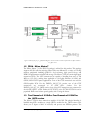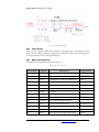
1
DINI GROUP LOGIC Emulation Source User Manual DNPCIe_10G_K7_LL (_QSFP) LOGIC EMULATION SOURCE DNPCIe_10G_K7_LL (_QSFP) User Manual Version 1.0 Date of Print December 12, 2012 Dini Group 7469 Draper Ave. La Jolla, CA92037 Phone 858.454.3419 • Fax 858.454.1728 [email protected] www.dinigroup.com Copyright Notice and Proprietary Information Copyright © 2012 Dini Group. All rights reserved. No part of this copyrighted work may be reproduced, modified or distributed in any form or by any means, without the prior written permission of the Dini Group. Right to Copy Documentation Dini Group permits licensee to make copies of the documentation for its internal use only. Each copy shall include all copyrights, trademarks, disclaimers and proprietary rights notices. Disclaimer Dini Group has made reasonable efforts to ensure that the information in this document is accurate and complete. However, the Dini Group assumes no liability for errors, or for any incidental, consequential, indirect, or special damages, including, without limitation, loss of use, loss or alteration of data, delays, or lost profits or savings, arising from the use of this document or the product which it accompanies. Table of Contents INTRODUCTION ............................................................................................................................................................................................................... 1 1 1.1 1.2 1.3 1.4 1.5 1.6 1.7 1.8 2 3 4 5 DNPCIE_10G_K7_LL (_QSFP) ETHERNET PACKET ANALYSIS ENGINE................................................................................................... 1 Overview............................................................................................................................................................................................................ 1 FPGA – Xilinx, Kintex-7 .................................................................................................................................................................................... 1 Two Channels of 10 GbE or Four Channels of 10 GbE for the _QSFP version ................................................................................................ 2 QDR II+ SSRAM - Memory with the Lowest Latency ........................................................................................................................................ 2 DDR3 DRAM - Bulk Memory ............................................................................................................................................................................ 2 PCI Express – Customizable 4-lane, GEN2 PCI Express .................................................................................................................................. 3 Time Synchronization ........................................................................................................................................................................................ 3 How Everything Works ….................................................................................................................................................................................. 3 DNPCIE_10G_K7_LL (_QSFP) ETHERNET PACKET ANALYSIS ENGINE FEATURES ................................................................................. 4 PACKAGE CONTENTS: ................................................................................................................................................................................ 6 INSPECT THE BOARD .................................................................................................................................................................................. 6 ADDITIONAL INFORMATION ....................................................................................................................................................................... 7 GETTING STARTED ........................................................................................................................................................................................................ 8 1 1.1 1.2 2 2.1 3 3.1 3.2 4 BEFORE YOU BEGIN ................................................................................................................................................................................... 8 Configuring the Programmable Components .................................................................................................................................................... 8 Warnings ........................................................................................................................................................................................................... 8 INSTALLING THE SOFTWARE ...................................................................................................................................................................... 8 Exploring the Customer Support Package ......................................................................................................................................................... 9 BOARD SETUP ............................................................................................................................................................................................ 9 Before Powering Up the Board .......................................................................................................................................................................... 9 Powering Up the Board ................................................................................................................................................................................... 10 USING THE REFERENCE DESIGN (MAIN) .................................................................................................................................................. 11 PROGRAMMING/CONFIGURING THE HARDWARE............................................................................................................................................. 13 1 2 2.1 2.2 2.3 3 3.1 3.2 3.3 4 4.1 4.2 4.3 INTRODUCTION ........................................................................................................................................................................................ 13 CONFIGURING THE FPGA USING JTAG.................................................................................................................................................... 14 Setup - Configuring the FPGA using JTAG ..................................................................................................................................................... 14 Powering Up the Board ................................................................................................................................................................................... 14 Configuring the FPGA ..................................................................................................................................................................................... 14 CONFIGURING THE FPGA USING MASTER BPI......................................................................................................................................... 16 Setup - Configuring the FPGA using Master BPI ............................................................................................................................................ 17 Powering Up the Board ................................................................................................................................................................................... 17 Configuring the FPGA ..................................................................................................................................................................................... 17 USING CHIPSCOPE PRO (VIA JTAG) ......................................................................................................................................................... 19 Setup – Using ChipScope Pro (via JTAG) ....................................................................................................................................................... 19 Powering Up the Board ................................................................................................................................................................................... 20 Configuring the FPGA ..................................................................................................................................................................................... 20 HARDWARE DESCRIPTION ........................................................................................................................................................................................ 21 1 1.1 1.2 1.3 1.4 DESCRIPTION ........................................................................................................................................................................................... 21 Overview.......................................................................................................................................................................................................... 21 FPGA – Xilinx, Kintex-7 .................................................................................................................................................................................. 22 Two Channels of 10 GbE or Four Channels of 10 GbE for the _QSFP version .............................................................................................. 22 QDR II+ SSRAM - Memory with the Lowest Latency ...................................................................................................................................... 23 1.5 1.6 1.7 2 3 4 5 6 DDR3 DRAM - Bulk Memory .......................................................................................................................................................................... 23 PCI Express – Customizable 4-lane, GEN2 PCI Express ................................................................................................................................ 23 Time Synchronization ...................................................................................................................................................................................... 24 FPGA (KINTEX-7).................................................................................................................................................................................... 24 2.1 FPGA Configuration ....................................................................................................................................................................................... 24 2.2 USB Port (RS232/JTAG) ................................................................................................................................................................................. 24 2.2.1 RS232/JTAG Circuit Diagram ................................................................................................................................................................. 24 2.2.2 Connections between FPGA and the RS232 Port..................................................................................................................................... 25 2.3 QDR II+ SRAM Memory ................................................................................................................................................................................. 25 2.3.1 QDRII+ SRAM Memory Architecture .................................................................................................................................................... 26 2.3.2 Design Guidelines – QDR II+ SRAM IO Standards ................................................................................................................................ 26 2.3.3 Connections between FPGA and QDR II+ SRAM Devices (4M x 18) .................................................................................................... 27 2.4 DDR3 Memory (VLP MINIUDIMM) ............................................................................................................................................................... 29 2.4.1 DDR3 SDRAM Memory Interface Solution ............................................................................................................................................ 29 2.4.2 Design Guidelines - DDR3 Termination .................................................................................................................................................. 30 2.4.3 Design Guidelines – DDR3 IO Standards ................................................................................................................................................ 31 2.4.4 Serial Presence-Detect EEPROM Operation............................................................................................................................................ 31 2.4.5 Clocking Connections between FPGA and MINIUDIMM ...................................................................................................................... 32 2.4.6 Connections between FPGA and MINIUDIMM ...................................................................................................................................... 32 2.5 EEPROM ......................................................................................................................................................................................................... 37 2.5.1 EEPROM Circuit Diagram ...................................................................................................................................................................... 37 2.5.2 Connections between FPGA and the EEPROM ....................................................................................................................................... 37 2.6 PCI Express Interface (x4)............................................................................................................................................................................... 37 2.6.1 System Requirements .............................................................................................................................................................................. 38 2.6.2 Clocking - Jitter Attenuator...................................................................................................................................................................... 38 2.6.3 PCI Express Circuit ................................................................................................................................................................................. 38 2.6.4 Connections between FPGA and PCI Express Edge Connector ............................................................................................................... 38 2.7 SFP+ Interface (only for DNPCIe_10G_K7_LL) ............................................................................................................................................ 39 2.7.1 SFP+ Circuit Diagram ............................................................................................................................................................................. 39 2.7.2 LED indicators ......................................................................................................................................................................................... 40 2.7.3 SFP+ Pin Assignments............................................................................................................................................................................. 41 2.7.4 Connections between FPGA and the SFP+ Connectors ........................................................................................................................... 41 2.8 QSFP+ Interface (only for the DNPCIe_10G_K7_LL_QSFP) ........................................................................................................................ 43 2.8.1 QSFP+ Circuit Diagram........................................................................................................................................................................... 43 2.8.2 LED indicators ......................................................................................................................................................................................... 44 2.8.3 QSFP+ Pin Assignments.......................................................................................................................................................................... 44 2.8.4 Connections between FPGA and the QSFP+ Connectors ........................................................................................................................ 45 2.9 Time Synchronization ...................................................................................................................................................................................... 46 2.9.1 Time Synchronization Circuit Diagram ................................................................................................................................................... 47 2.9.2 Connections between the FPGA and Time Synchronization Circuitry ..................................................................................................... 47 CLOCK GENERATION................................................................................................................................................................................ 48 3.1 System Clock – IDELAYCTRL ......................................................................................................................................................................... 48 3.1.1 Connection between FPGA and the System Clock Oscillator .................................................................................................................. 48 3.2 High-Speed (GTX) Clocks ............................................................................................................................................................................... 48 LED INDICATORS ..................................................................................................................................................................................... 48 4.1 FPGA Status LEDs .......................................................................................................................................................................................... 48 4.2 Configuration DONE LEDs ............................................................................................................................................................................. 49 POWER DISTRIBUTION.............................................................................................................................................................................. 49 5.1 In-System Operation ........................................................................................................................................................................................ 49 MECHANICAL ........................................................................................................................................................................................... 49 6.1 Board Dimensions ........................................................................................................................................................................................... 49 APPENDIX 7 8 51 APPENDIX A: UCF FILE........................................................................................................................................................................... 51 ORDERING INFORMATION ........................................................................................................................................................................ 51 List of Figures Figure 1 - DNPCIe_10G_K7_LL (_QSFP) Ethernet Packet Analysis Engine. (upper picture is the DNPCIe_10G_K7_LL and lower picture is the DNPCIe_10G_K7_LL_QSFP) .................................................................................................................................................................................................... 4 Figure 2 - USB Flash Drive Directory Structure ............................................................................................................................................................................................. 9 Figure 3 - DNPCIe_10G_K7_LL (_QSFP) Block Diagram – Note the two SFP+ modules are replaced with one QSFP+ module in the _QSFP version ....... 22 Figure 4 –FPGA Serial Port ............................................................................................................................................................................................................................ 25 Figure 5 - QDR II+ Memory Architecture ................................................................................................................................................................................................... 26 Figure 6 –FPGA Serial Port ............................................................................................................................................................................................................................ 37 Figure 7 - SFP+ Channel 0 Interface ............................................................................................................................................................................................................. 40 Figure 8 – SFP+ GTX Oscillator ................................................................................................................................................................................................................... 40 Figure 9 - QSFP+ Channel 0 Interface .......................................................................................................................................................................................................... 43 Figure 10 – QSFP+ GTX Oscillator .............................................................................................................................................................................................................. 44 List of Tables Table 1 – USB Flash Drive Directory Contents ............................................................................................................................................................................................. 9 Table 2 – Kintex-7 Uncompressed Bitstream Length ..................................................................................................................................................................................16 Table 3 - Connections between RS232 Port and the FPGA .......................................................................................................................................................................25 Table 4 – QDR II+ SRAM IO Standards .....................................................................................................................................................................................................26 Table 5 - Connections between FPGA and the QDR II+ SRAM Devices ...............................................................................................................................................27 Table 6 - Serial Presence-Detect EEPROM Connections ...........................................................................................................................................................................31 Table 7 – Clocking Connections between FPGA and the UDIMM Connector .......................................................................................................................................32 Table 8 - Connections between FPGA and the UDIMM Connector ........................................................................................................................................................32 Table 9 - Connections between FPGA and the EEPROM .........................................................................................................................................................................37 Table 10 - Connections between FPGA and the PCI Express Edge Connector ......................................................................................................................................38 Table 11 – SFP+ Pin Assignments .................................................................................................................................................................................................................41 Table 12 - Connections between FPGA and the SFP+ Connectors ..........................................................................................................................................................42 Table 13 – QSFP+ Pin Assignments..............................................................................................................................................................................................................44 Table 14 - Connections between FPGA and the QSFP+ Connectors.......................................................................................................................................................45 Table 15 - Connection between the FPGA and the System Clock Oscillator ...........................................................................................................................................48 Table 16 – FPGA Status LEDs.......................................................................................................................................................................................................................48 Table 17 – FPGA DONE LED .....................................................................................................................................................................................................................49 1 Chapter I N T R O D U C T I O N Introduction This User Manual accompanies the DNPCIe_10G_K7_LL (_QSFP) Ethernet Packet Analysis Engine. For specific information regarding the Xilinx Kintex-7 parts, please reference the datasheet on the Xilinx website. 1 DNPCIe_10G_K7_LL (_QSFP) Ethernet Packet Analysis Engine 1.1 Overview The DNPCIe_10G_K7_LL (_QSFP) is a PCI Express based FPGA board designed to minimize input to output processing latency on 10Gb Ethernet packets. The primary application is for ultra-low latency, high throughput trading without CPU intervention. Every possible variable that affects input to output latency has been analyzed and minimized. Raw 10 GbE packets can be analyzed and acted upon without interrupts or an operating system adding delay to the process. This configurable hardware computing platform has the ability to achieve the theoretical minimum Ethernet packet processing latency. This board also has a time code input to allow for precise message time stamping and tracking. 1.2 FPGA – Xilinx, Kintex-7 The Xilinx, Kintex-7, in the FFG676 package is utilized for this product. This package supports 400 IOs with the majority utilized. Most are dedicated to a variety of off chip memory peripherals including QDR II+ for low-latency, high speed look-up, and DDR3 for performance oriented bulk storage. The Kintex-7 FPGAs contain high-speed transceiver PHYs. The GTX transceivers are capable of handling data rates of 500 Mb/s to 12.5 Gb/s, making these applicable to 10 Gigabit Ethernet (10 GbE) and GEN1/GEN2 PCI Express applications. Four of the GTX transceivers are used for GEN2-capable PCIe. For the DNPCIe_10G_K7_LL version, two of the GTX transceivers are connected to 10 GbE SFP+ sockets. For the DNPCIe_10G_K7_LL_QSFP version, four of the GTX transceivers are connected to the 40 GbE QSFP+ socket. DNPCIe_10G_K7_LL (_QSFP) User Manual www.dinigroup.com 1 I N T R O D U C T I O N Either the XC7K325T or the XC7K410T FPGAs can be populated. Both come in three speeds grades, with -3 being the fastest. 1.3 Two Channels of 10 GbE or Four Channels of 10 GbE for the _QSFP version The Kintex-7 FPGAs have transceivers capable of 10 GbE. The physical interface is handled using SFP+ modules or a single QSFP+ module for the _QSFP verison. This allows you to bypass a MAC if necessary and process raw Ethernet packets. The DNPCIe_10G_K7_LL has two 10 GbE channels and the DNPCIe_10G_K7_LL_QSFP has four 10 GbE channel, and can support 10GBASET-ER, 10GBASET-SR, 10GBASET-KR. 1.4 QDR II+ SSRAM - Memory with the Lowest Latency One, quad data rate, static RAMs (QDR II+ SSRAM) is used in the 4M x 18 size. This style of memory has separate input and output data paths, enabling maximum read/write data bandwidth with minimum latency. Using -3 speed grade FPGA, this interface is capable of running at the maximum I/O frequency of 500MHz. To minimize processing latency, we suspect it will be best to clock these QDRII+ SSRAMs at 312.50 MHz, exactly twice the internal Ethernet controller frequency of 156.25MHz. The Kintex-7 FPGAs are capable of generating internal 2x clocks that are phase synchronous, eliminating the latencies associated with the tricky re-synchronization of data moving between different clock frequencies. The internal controller can be optimized in any way you choose. Dini Group provides several Verilog examples. All functions of the QDR II+ SSRAM can be exploited, including concurrent read and write operations and four-tick bursts. The only real limitation is the amount of time and effort spent in customizing the individual memory controllers. 1.5 DDR3 DRAM - Bulk Memory A single 244-pin PC3-10600 DDR3 VLP MINIUDIMM socket enables up to 4GB of memory for bulk storage and lookup. Using a -2 or -3 speed grade FPGA, this interface is tested at the maximum FPGA I/O frequency: 666.5Hz (1333Mb/s with DDR). The user can use this memory as 64-bits with 8 bits of error correction (ECC), or as a 72-bit byte-memory without correction. To minimize data synchronization across clock boundaries, it probably makes sense to clock the DDR3 interface at a 3x multiple of the base Ethernet frequency of 156.25 MHz, which is 468.75MHz. A 3x phase synchronous clock can be easily generated internal to the FPGA, allowing zero latency synchronous data transfers between the Ethernet packet receiving logic and the DDR3 memory controller. The DDR3 controller can be optimized in any way you choose. We, of course, provide several Verilog examples. All functions of the DDR3 DRAM can be exploited and optimized. Timing variables such as CAS latency and precharge can be tailored to the minimum given your operating frequency and the timing specification of the exact DDR3 memory DNPCIe_10G_K7_LL (_QSFP) User Manual www.dinigroup.com 2 I N T R O D U C T I O N utilized. As with the QDRII+ SRAM, the only real limitation is the amount of time and effort spent customizing the DDR3 memory controller to your needs. 1.6 PCI Express – Customizable 4-lane, GEN2 PCI Express PCI Express is connected directly to the FPGA via 4-lanes of GTX transceivers. The interfaces are GEN2 capable, and the board is shipped with PCIe IP that is a full function, fixed, 4-lane master/target. To gain access to the PCIe interface, this IP must be integrated with the user application. Dini Group provides support with the IP, including BAR sizes. Additionally we can optionally add or subtract DMA engines, scratchpad memories, interrupts, and other host-related functions to maximize the performance, while utilizing the minimum FPGA resources. 'C' source for drivers for several operating systems are included no charge. Partial reconfiguration of the FPGA is supported via the PCIe interface. 1.7 Time Synchronization The time code input allows for precise message time stamping and tracking. This input can receiver PPS, or IRIG-B000 (RS232, RS485, RS422, TLL). 1.8 How Everything Works … With direct data feeds such as NASDAQ (ITCH/OUCH) or Financial Information Exchange (FIX), the DNPCIe_10G_K7_LL (_QSFP) contains all of the basic functions required to minimize the amount of time it takes to receive Ethernet packets, process them, and respond deterministically. The MAC, operating system et al, can be bypassed. There are no interrupts. No operating system. Not a single clock cycle is wasted here, enabling a near theoretical minimum in-to-out response time. For algorithms requiring processing, FPGA resources can be hard coded to perform the task. This includes real-time Monte Carlo analysis and floating point, all operating 1000's of times faster than possible in a processor-based approach. DNPCIe_10G_K7_LL (_QSFP) User Manual www.dinigroup.com 3 I N T R O D U C T I O N 2 DNPCIe_10G_K7_LL (_QSFP) Ethernet Packet Analysis Engine Features Figure 1 - DNPCIe_10G_K7_LL (_QSFP) Ethernet Packet Analysis Engine. (upper picture is the DNPCIe_10G_K7_LL and lower picture is the DNPCIe_10G_K7_LL_QSFP) DNPCIe_10G_K7_LL (_QSFP) Kintex-7 Board features the following: Hosted in a 4-lane (16-lane mechanical, with notches to allow to be plugged into x4/x8/x16) PCI Express Slot (GEN2) or Stand-alone Xilinx Kintex-7 FPGA (FFG676) o XC7K325T (-3, -2, -1 fastest to slowest) o XC7K410T (-3, -2, -1 fastest to slowest) GTX Transceivers (10Gb/s) o PCI Express (x4) o Two SFP+ modules (x1 each) o QSFP+ module (x4), only with _QSFP version DNPCIe_10G_K7_LL (_QSFP) User Manual www.dinigroup.com 4 I N T R O D U C T I O N Flexible Clock Resources o PCI Express Clock Jitter Attenuator – 250MHz o Oscillators for GTX Transceivers Memory o Bulk Memory: DDR3 VLP MINIUDIMM (244-pin) 72-bit data width (64-bit with 8-bit ECC) PC3-10600 (666.5MHz) Addressing/power to support 4GB (+ ECC) DDR3 Verilog/VHDL reference design provided. o QDRII + SSRAM 1 channels: 4M x 18 (72Mb) 500 MHz bus operation, DDR (double data rate) Fast enough to be clocked at 312.50 MHz Eliminates clock synchronization delays between memory and Ethernet clock. User LED’s Time Synchronization o 2.5mm jack that accepts PPS (RS232/RS485/RS422/TTL) time code. Onboard Distributed Power Supplies Full support for Embedded Logic Analyzers and Debug and IRIG-B000 o ChipScope Logic Analyzer o InPA, Veridae, SpringSoft USB-B 2.0 Port o RS232 o JTAG The FIX board support package (DN_FBSP) for the DNPCIe_10G_K7_LL (_QSFP) is a functioning reference design with the following components: o 10-Gigabit Ethernet MAC o TCP/IP Offload Engine (TOE) o FIX protocol parser DNPCIe_10G_K7_LL (_QSFP) User Manual www.dinigroup.com 5 I N T R O D U C T I O N o PCIe Interface (4-lane, GEN2) o Memory o QDRII+ Controller o DDR3 Controller 3 Package Contents: Before using the kit or installing the software, be sure to check the contents of the kit and inspect the board to verify that you received all of the items. If any of these items are missing, contact Dini Group before you proceed. The DNPCIe_10G_K7_LL (_QSFP) Ethernet Packet Analysis Engine includes the following: USB Flash Drive (4GB) – USB007, P/N UFDCR-4096 USB 2.0 Cable – NewEgg, P/N N82E16812119030 VLP MINIUDIMM DDR3 2GB (PC3-10600), 244 Pin, Micron, P/N MT9JBG25672AKZ-1G4 DB9 to 2.5mm cable. P/N BC20223-6 Customer Support Package (on USB Flash Drive) o Documentation (Datasheets, User Manual and Schematics) o FPGA Reference Designs (Verilog) o Host Software (AETest) Optional Items SFP+ Direct Cable 10GbE Copper, 1.6ft – Amphenol, P/N SF-SFPP2EPASS000.5 4 Inspect the Board Place the board on an anti-static surface and inspect it to ensure that it has not been damaged during shipment. Verify that all components are on the board and appear intact. DNPCIe_10G_K7_LL (_QSFP) User Manual www.dinigroup.com 6 I N T R O D U C T I O N 5 Additional Information For additional information, please visit http://www.dinigroup.com/. The following table lists some of the resources you can access from this website. You can also directly access these resources using the provided URLs. Resource Description/URL User Manual This is the main source of technical information. The manual should contain most of the answers to your questions Demonstration Videos MEG-Array Daughter Card header insertion and removal video Dini Group Web Site The web page will contain the latest user manual, application notes, FAQ, articles, and any device errata and manual addenda. Please visit and bookmark: http://www.dinigroup.com Data Book Pages from 7-Series Databook, which contains device-specific information on Xilinx device characteristics E-Mail You may direct questions and feedback to Dini Group using this email address: [email protected] Phone Support Call us at 858.454.3419 during the hours of 8:00am to 5:00pm Pacific Time. FAQ The download section of the web page may contain a document called DNPCIe_10G_K7_LL (_QSFP) Frequently Asked Questions (FAQ). This document is periodically updated with information that may not be in the User’s Manual. DNPCIe_10G_K7_LL (_QSFP) User Manual www.dinigroup.com 7 G E T T I N G 2 Chapter S T A R T E D Getting Started Congratulations on your purchase of the DNPCIe_10G_K7_LL (_QSFP) Ethernet Packet Analysis Engine. The remainder of this chapter describes how to start using the DNPCIe_10G_K7_LL (_QSFP) Ethernet Packet Analysis Engine. 1 Before You Begin 1.1 Configuring the Programmable Components The DNPCIe_10G_K7_LL (_QSFP) has been factory tested and pre-programmed to ensure correct operation. The user does not need to alter any jumpers or program anything to see the board work. 1.2 Warnings Mechanical Stress – Inserting and removing VLP MINIUDIMM and the board from the motherboard can add additional stress that may cause board failures. ESD Warning - The board is sensitive to static electricity, so treat the PCB accordingly. The target markets for this product are engineers that are familiar with FPGAs and circuit boards. However, if needed, the following web page has an excellent tutorial on the “Fundamentals of ESD” for those of you who are new to ESD sensitive products: http://en.wikipedia.org/wiki/Electrostatic_discharge 2 Installing the Software No Software installation required. DNPCIe_10G_K7_LL (_QSFP) User Manual www.dinigroup.com 8 G E T T I N G S T A R T E D 2.1 Exploring the Customer Support Package The USB Flash Drive contains the following items, see Figure 2: Documentation FPGA Reference Designs Host Software Figure 2 - USB Flash Drive Directory Structure A description of the USB Flash Drive directory contents is listed in Table 1. Please visit the Dini Group website for the most recent revision of these documents. Table 1 – USB Flash Drive Directory Contents USB Flash Drive Directory Contents Directory Name Description of Contents Documentation Contains the Datasheets, Schematics and User Manual for the board. FPGA Reference Designs Contains the source and compiled programming files for the DNPCIe_10G_K7_LL (_QSFP) reference designs. Host Software Provides the Host Software for the Windows and Linux platforms. 3 Board Setup The instructions in this section explain how to install the DNPCIe_10G_K7_LL (_QSFP) Ethernet Packet Analysis Engine. For the purpose of this demonstration, the DNPCIe_10G_K7_LL (_QSFP) will be configured using a motherboard’s PCIE connectors for power and the USB interface. 3.1 Before Powering Up the Board Before powering up the board, prepare the board as follows: 1. If the kit contains a Memory VLP MINIUDIMM module, populate the VLP MINIUDIMM socket J7. DNPCIe_10G_K7_LL (_QSFP) User Manual www.dinigroup.com 9 G E T T I N G S T A R T E D 2. Plug board into x4, x8, or x16 PCIE slot. 3. Connect the “USB 2.0 Cable” to the USB-B connector on the bracket. Note: The DNPCIe_10G_K7_LL (_QSFP) Ethernet Packet Analysis Engine is shipped with a passive heat sink for operation in a server or PC with forced cooling. If the board is used in standalone mode, please provide an external fan to prevent the FPGA from overheating! 3.2 Powering Up the Board 1. Power up the board by turning ON the power to the motherboard verify the “+12V” LED (DS16) is ON indicating the presence of +12V (located on the back-side of the board near the top-left.) 2. USB drivers should automatically install when the board turns on. If this doesn’t happen then install the USB driver from the FTDI website (for driver installation, please refer to http://www.ftdichip.com/Support/Documents/InstallGuides.htm). 3. Once drivers are finished installing, open a Terminal Emulator and configure the session as follows: DNPCIe_10G_K7_LL (_QSFP) User Manual www.dinigroup.com 10 G E T T I N G S T A R T E D 4 Using the Reference Design (Main) This section lists detailed instructions for executing the reference design. Ensure the DNPCIe_10G_K7_LL (_QSFP) Ethernet Packet Analysis Engine is powered ON and a Terminal Window is open to exercise the reference design options; 1. Select test option (6), “Clock Frequencies Check” in the Terminal window and verify that the test displays VALID frequencies. 2. Select test option (0), “DDR3 Test (requires ECC module)” in the Terminal window and verify that the test PASS (periods will be displayed as the memory locations are being tested, if no DDR3 Module is present, the test will display read/write errors). DNPCIe_10G_K7_LL (_QSFP) User Manual www.dinigroup.com 11 G E T T I N G S T A R T E D 3. Select test option (3), “QDR2 Test” in the Terminal window and verify that the test PASS (periods will be displayed as the memory locations are being tested, if no QDR2 Memory fails, the test will display read/write errors). The remainder of the reference design functional tests requires various loop-back test boards/modules to make them PASS, and is not covered in this User Manual. Please reference the Customer Support Package (on USB Flash Drive) for code examples. The next section describes configuring and programming the hardware in detail. DNPCIe_10G_K7_LL (_QSFP) User Manual www.dinigroup.com 12 P R O G R A M M I N G / C O N F I G U R I N G T H E H A R D W A R E 3 Chapter Programming/Configuring the Hardware This chapter details the programming and configuration instructions for the DNPCIe_10G_K7_LL (_QSFP) Ethernet Packet Analysis Engine. 1 Introduction This section of the User Manual presents different methods to configure the Xilinx Kintex-7 FPGA: Configuring the FPGA using JTAG – using the “USB 2.0 Cable”. Configuring the FPGA using Master BPI – using the BPI serial Flash PROM. Kintex-7 FPGAs are configured by loading application-specific configuration data - the bitstream - into internal memory. Because the Xilinx FPGA configuration memory is volatile, it must be configured each time it is powered-up. The bitstream is loaded into the device through special configuration pins. These configuration pins serve as the interface for a number of different configuration modes. The following configuration modes are supported: Master Byte Peripheral Interface (BPI) configuration mode (x16) JTAG/Boundary-Scan configuration mode The configuration modes are explained in detail in the UG470 – 7 Series FPGAs Configuration User Guide. The specific configuration mode is selected by setting the appropriate level on the dedicated Mode input pins M[2:0]. DNPCIe_10G_K7_LL (_QSFP) User Manual www.dinigroup.com 13 P R O G R A M M I N G / C O N F I G U R I N G T H E H A R D W A R E 2 Configuring the FPGA using JTAG This section lists detailed instructions for programming the Xilinx Kintex-7 FPGA using iMPACT, Version 14.2 tools. The JTAG/Boundary-Scan configuration interface is always available, regardless of the Mode pin settings. The JTAG/Boundary-Scan configuration mode disables all other configuration modes to prevent conflicts between configuration interfaces. Note: This User Manual will not be updated for every revision of the Xilinx ISE tools, so please be aware of minor differences. 2.1 Setup - Configuring the FPGA using JTAG Before configuring the FPGA, ensure the following steps have been completed: 1. Connect the “USB 2.0 Cable” to the bracket mounted USB 2.0 B connector. 2.2 Powering Up the Board 1. Power up the board by turning ON the ATX power supply to the motherboard and verify the “+12V” LED (DS16) is ON indicating the presence of +12V (located on the back-side of the board near the top-left.) 2.3 Configuring the FPGA To configure the Xilinx FPGA, perform the following steps: 2. Open iMPACT and create a new default project. Select “Configure devices using Boundary-Scan (JTAG)” from the iMPACT welcome menu. DNPCIe_10G_K7_LL (_QSFP) User Manual www.dinigroup.com 14 P R O G R A M M I N G / C O N F I G U R I N G T H E H A R D W A R E 3. iMPACT will identify the components in the JTAG chain. A pop-up window will display “ERROR: iMPACT – Bsdl reader is not available for device 3”. Click “OK” to proceed (Reason: QDR2 devices are also in the JTAG chain). 4. A pop-up window will display “Device Programming Properties – Device 1 Programming Properties”. Click “OK” to select default options. 5. Right-click on FPGA and select “Assign New Configuration File”. Specify the location for the FPGA bit file based on the type of FPGA populated e.g. XC7K325T; a pop-up window will display “Attach SPI or BPI PROM”. Click “NO” to proceed. 6. Right-click on the FPGA and select the “Program” option. Click “OK” in the “Device Programming Properties” window. A “Configuration Operation Status” box will appear indicating programming progress. DNPCIe_10G_K7_LL (_QSFP) User Manual www.dinigroup.com 15 P R O G R A M M I N G / C O N F I G U R I N G T H E H A R D W A R E 7. Verify that the “FPGA_DONE” blue LED (DS15) is enabled, indicating successful configuration of the FPGA. 3 Configuring the FPGA using Master BPI In Master Byte-wide Peripheral Interface (BPI) Mode, the Kintex-7 FPGA configures itself from an attached industry-standard, parallel NOR flash PROM. The board is populated with a Micron, PC28F00AG18F, 1-Gbit Flash PROM. Table 2 shows the uncompressed configuration file size for the supported Kintex-7 devices. Table 2 – Kintex-7 Uncompressed Bitstream Length Device XC7K325T XC7K410T Data Size (Bits) 91,548,896 127,023,328 PROM/Flash 28F00AG18F 28F00AG18F Note: This User Manual will not be updated for every revision of the Xilinx ISE tools, so please be aware of minor differences. DNPCIe_10G_K7_LL (_QSFP) User Manual www.dinigroup.com 16 P R O G R A M M I N G / C O N F I G U R I N G T H E H A R D W A R E 3.1 Setup - Configuring the FPGA using Master BPI Before configuring the FPGA, ensure the following steps have been completed: 1. Connect the “USB 2.0 Cable” to the bracket mounted USB 2.0 B connector. 3.2 Powering Up the Board 1. Power up the board by turning ON the ATX power supply to the motherboard and verify the “+12V” LED (DS16) is ON indicating the presence of +12V (located on the back-side of the board near the top-left.) 3.3 Configuring the FPGA To configure the Xilinx FPGA, perform the following steps: 1. Open iMPACT and create a new default project. Select “Configure devices using Boundary-Scan (JTAG)” from the iMPACT welcome menu. 2. iMPACT will identify the components in the JTAG chain. A pop-up window will display “ERROR: iMPACT – Bsdl reader is not available for device 3”. Click “OK” to proceed (Reason: QDR2 devices are also in the JTAG chain). 3. A pop-up window will display “Device Programming Properties – Device 1 Programming Properties”. Click “OK” to select default options. DNPCIe_10G_K7_LL (_QSFP) User Manual www.dinigroup.com 17 P R O G R A M M I N G / C O N F I G U R I N G T H E H A R D W A R E 4. Right-click on FPGA and select “Add BPI/SPI Flash”. Specify the location for the PROM file based on the type of FPGA populated e.g. XC7K325T; 5. Select the 28F00AG18F device in the “Select Attached SPI/BPI” window. 6. Right-Click on the “FLASH” icon and select “Program”. Uncheck the “Verify” checkbox followed by “OK”. A Process Dialog box will indicate programming progress. Note: This process takes minutes to complete! 7. Verify that iMPACT successfully programmed the BPI Flash. DNPCIe_10G_K7_LL (_QSFP) User Manual www.dinigroup.com 18 P R O G R A M M I N G / C O N F I G U R I N G T H E H A R D W A R E 8. Power-cycle the board and verify that the “FPGA_DONE” blue LED (DS15) is enabled, indicating successful configuration of the FPGA from BPI PROM. 4 Using ChipScope Pro (via JTAG) The Xilinx ChipScope Pro tool inserts logic analyzer, system analyzer, and virtual I/O low-profile software cores directly into the design, allowing the user to view any internal signal or node, including embedded hard or soft processors. Signals are captured in the system at the speed of operation and brought out through the programming interface, freeing up pins for your design. Captured signals are then displayed and analyzed using the ChipScope Pro Analyzer tool Note: This User Manual will not be updated for every revision of the Xilinx ISE tools, so please be aware of minor differences. 4.1 Setup – Using ChipScope Pro (via JTAG) Before configuring the FPGA, ensure the following steps have been completed: 1. Connect the “USB 2.0 Cable” to the bracket mounted USB 2.0 B connector. DNPCIe_10G_K7_LL (_QSFP) User Manual www.dinigroup.com 19 P R O G R A M M I N G / C O N F I G U R I N G T H E H A R D W A R E 4.2 Powering Up the Board 1. Power up the board by turning ON the ATX power supply to the motherboard and verify the “+12V” LED (DS16) is ON indicating the presence of +12V (located on the back-side of the board near the top-left.) 4.3 Configuring the FPGA To configure the Xilinx FPGA, perform the following steps (Note: Non-Xilinx devices in the JTAG chain will report IR Length errors): 1. Open ChipScope Pro -> Analyzer and identify the devices in the JTAG chain. Note: In order for the JTAG offsets to be set correctly, set the IR Length for the QDR SRAMs to 3. 2. Proceed as normal, see UG029 - ChipsCope Pro Software and Cores User Guide. DNPCIe_10G_K7_LL (_QSFP) User Manual www.dinigroup.com 20 H A R D W A R E 4 Chapter D E S C R I P T I O N Hardware Description This chapter describes the hardware features of the DNPCIe_10G_K7_LL (_QSFP) Ethernet Packet Analysis Engine. 1 Description 1.1 Overview The DNPCIe_10G_K7_LL (_QSFP) is a PCI Expressed based FPGA board designed to minimize input to output processing latency on 10Gb/s Ethernet packets. The primary application is for ultra-low latency, high throughput trading without CPU intervention. Every possible variable that affects input to output latency has been analyzed and minimized. Raw 10 GbE Ethernet packets can be analyzed and acted upon without interrupts or an operating system adding delay to the process. This configurable hardware computing platform has the ability to achieve the theoretical minimum Ethernet packet processing latency. A high level block diagram of the DNPCIe_10G_K7_LL (_QSFP) Ethernet Packet Analysis Engine is shown in Figure 3, followed by a brief description of each section. DNPCIe_10G_K7_LL (_QSFP) User Manual www.dinigroup.com 21 H A R D W A R E D E S C R I P T I O N Figure 3 - DNPCIe_10G_K7_LL (_QSFP) Block Diagram – Note the two SFP+ modules are replaced with one QSFP+ module in the _QSFP version 1.2 FPGA – Xilinx, Kintex-7 The Xilinx, Kintex-7, in the FFG676 package is utilized for this product. This package supports 400 IOs with the majority utilized. Most are dedicated to a variety of off chip memory peripherals including QDR II+ for low-latency, high speed look-up, and DDR3 for performance oriented bulk storage. The Kintex-7 FPGAs contain high-speed transceiver PHYs. The GTX transceivers are capable of handling data rates of 500 MB/s to 12.5 Gb/s, making these applicable to 10 Gigabit Ethernet (10 GbE) and GEN1/GEN2 PCI Express applications. Four of the GTX transceivers are used for GEN2-capable PCIe. For the DNPCIe_10G_K7_LL version, two of the GTX transceivers are connected to 10 GbE SFP+ sockets. For the DNPCIe_10G_K7_LL_QSFP version, four of the GTX transceivers are connected to the 40 GbE QSFP+ socket. Either the XC7K325T or the XC7K410T FPGAs can be populated. Both come in three speeds grades, with -3 being the fastest. 1.3 Two Channels of 10 GbE or Four Channels of 10 GbE for the _QSFP version The Kintex-7 FPGAs have transceivers capable of 10 GbE. The physical interface is handled using SFP+ modules or a single QSFP+ module for the _QSFP verison. This allows you to bypass a MAC if necessary and process raw Ethernet packets. The DNPCIe_10G_K7_LL (_QSFP) User Manual www.dinigroup.com 22 H A R D W A R E D E S C R I P T I O N DNPCIe_10G_K7_LL has two 10 GbE channels and the DNPCIe_10G_K7_LL_QSFP has four 10 GbE channel, and can support 10GBASET-ER, 10GBASET-SR, 10GBASET-KR. 1.4 QDR II+ SSRAM - Memory with the Lowest Latency One, quad data rate, static RAMs (QDR II+ SSRAM) is used in the 4M x 18 size. This style of memory has separate input and output data paths, enabling maximum read/write data bandwidth with minimum latency. Using -3 speed grade FPGA, this interface is capable of running at the maximum I/O frequency of 500MHz. To minimize processing latency, we suspect it will be best to clock these QDRII+ SSRAMs at 312.50 MHz, exactly twice the internal Ethernet controller frequency of 156.25MHz. The Kintex-7 FPGAs are capable of generating internal 2x clocks that are phase synchronous, eliminating the latencies associated with the tricky re-synchronization of data moving between different clock frequencies. The internal controller can be optimized in any way you choose. Dini Group provides several Verilog examples. All functions of the QDR II+ SSRAM can be exploited, including concurrent read and write operations and four-tick bursts. The only real limitation is the amount of time and effort spent in customizing the individual memory controllers. 1.5 DDR3 DRAM - Bulk Memory A single 244-pin PC3-10600 DDR3 VLP MINIUDIMM socket enables up to 4GB of memory for bulk storage and lookup. Using a -2 or -3 speed grade FPGA, this interface is tested at the maximum FPGA I/O frequency: 666.5MHz (1333Mb/s with DDR). The user can use this memory as 64-bits with 8 bits of error correction (ECC), or as a 72-bit byte-memory without correction. To minimize data synchronization across clock boundaries, it probably makes sense to clock the DDR3 interface at a 3x multiple of the base Ethernet frequency of 156.25 MHz, which is 468.75MHz. A 3x phase synchronous clock can be easily generated internal to the FPGA, allowing zero latency synchronous data transfers between the Ethernet packet receiving logic and the DDR3 memory controller. The DDR3 controller can be optimized in any way you choose. We, of course, provide several Verilog examples. All functions of the DDR3 DRAM can be exploited and optimized. Timing variables such as CAS latency and precharge can be tailored to the minimum given your operating frequency and the timing specification of the exact DDR3 memory utilized. As with the QDRII+ SRAM, the only real limitation is the amount of time and effort spent customizing the DDR3 memory controller to your needs. 1.6 PCI Express – Customizable 4-lane, GEN2 PCI Express PCI Express is connected directly to the FPGA via 4-lanes of GTX transceivers. The interfaces are GEN2 capable, and the board is shipped with PCIe IP that is a full function, fixed, 4-lane master/target. To gain access to the PCIe interface, this IP must be integrated with the user application. Dini Group provides support with the IP, including BAR sizes. Additionally we can optionally add or subtract DMA engines, scratchpad memories, interrupts, and other host-related functions to maximize the DNPCIe_10G_K7_LL (_QSFP) User Manual www.dinigroup.com 23 H A R D W A R E D E S C R I P T I O N performance, while utilizing the minimum FPGA resources. 'C' source for drivers for several operating systems are included no charge. Partial reconfiguration of the FPGA is supported via the PCIe interface. 1.7 Time Synchronization The time code input allows for precise message time stamping and tracking. This input can receiver PPS, or IRIG-B000 (RS232, RS485, RS422, TLL). 2 FPGA (Kintex-7) 2.1 FPGA Configuration Kintex-7 FPGAs are configured by loading application-specific configuration data - the bitstream - into internal memory. Because the Xilinx FPGA configuration memory is volatile, it must be configured each time it is powered-up. The bitstream is loaded into the device through special configuration pins. These configuration pins serve as the interface for a number of different configuration modes. The following configuration modes are supported: Master BPI (x16) JTAG/Boundary-Scan The FPGA drives up to 26 address lines to access the attached parallel flash. For configuration from industry-standard parallel NOR flash, only asynchronous read mode is used. In asynchronous read mode, the FPGA drives the address bus and the flash PROM drives back the bitstream data. Using the JTAG interface, the Kintex-7 FPGA can be configured using Xilinx software (iMPACT or ChipScope software) and “USB 2.0 Cable”. 2.2 USB Port (RS232/JTAG) A RS232/JTAG ports (U15) are provided for low speed communication/programming and debugging with the Kintex-7 FPGA. The FT2232H is a USB to JTAG/UART interface device which simplifies USB to serial designs and reduces external component count by fully integrating an external EEPROM, and USB termination resistors. It has been designed to operate efficiently with a USB host controller by using as little as possible of the total USB bandwidth available. 2.2.1 RS232/JTAG Circuit Diagram Figure 4 shows the implementation of the USB port. DNPCIe_10G_K7_LL (_QSFP) User Manual www.dinigroup.com 24 H A R D W A R E D E S C R I P T I O N Figure 4 –FPGA Serial Port There are two signals attached to the FPGA for RS232 communication: Transmit Data – USB_B_TXD Receive Data – USB_B_RXD The USB Transceiver Cell provides the USB 1.1 / USB 2.0 full-speed physical interface to the USB cable. 2.2.2 Connections between FPGA and the RS232 Port The connections between the FPGA and the RS232 Port are shown in Table 3. Table 3 - Connections between RS232 Port and the FPGA Signal Name USB_B_TXD USB_B_RXD FPGA U6-G11 U6-F10 RS232 U15-38 U15-39 2.3 QDR II+ SRAM Memory The CY7C25632KV18-500BZC is a 1.8 V synchronous pipelined SRAM, equipped with QDR II+ architecture. Similar to QDR II architecture, QDR II+ architecture consists of two separate ports: the read port and the write port to access the memory array. The read port has dedicated data outputs to support read operations and the write port has dedicated data inputs to support write operations. QDR II+ architecture has separate data inputs and data outputs to completely eliminate the need to “turn-around” the data bus that exists with common I/O devices. Each port is accessed through a common address bus. Addresses for read and write addresses are latched on alternate rising edges of the input (K) clock. Accesses to the QDR II+ read and write ports are completely independent of one another. To maximize data throughput, both read and write ports are equipped with DDR interfaces. Each address location is associated with four 18-bit words that burst sequentially into or out of the device. Because data is DNPCIe_10G_K7_LL (_QSFP) User Manual www.dinigroup.com 25 H A R D W A R E D E S C R I P T I O N transferred into and out of the device on every rising edge of both input clocks (K and Kn), memory bandwidth is maximized while simplifying system design by eliminating bus “turn-arounds”. These devices have an on-die termination feature supported for D[x:0], BWS[x:0], and K/K inputs, which helps eliminate external termination resistors, reduce cost, reduce board area, and simplify board routing. 2.3.1 QDRII+ SRAM Memory Architecture One QDR II+ SRAM memory (U4) is connected in a 4M x18 memory architecture, see Figure 5. The Memory Interface Generator (MIG) is a self-explanatory wizard tool that can be invoked under the CORE Generator software. Xilinx published a memory application note; please refer to UG-586 – 7-Series FPGAs Memory Interface Solutions, User Guide. Figure 5 - QDR II+ Memory Architecture The memory is also mapped into the JTAG chain and is fully compliant with IEEE Standard #1149.1-2001. 2.3.2 Design Guidelines – QDR II+ SRAM IO Standards The MIG tool generates the appropriate UCF file for the core with select I/O standards based on the type of input or output to the Kintex-7 FPGA. These standards should not be changed. Table 4 contains a list of the ports together with the I/O standard used. Table 4 – QDR II+ SRAM IO Standards Signal Name qdriip_bw_n qdriip_cq_p, qdriip_cq_n qdriip_d qdriip_k_p, qdriip_k_n qdriip_q Direction OUTPUT INPUT OUTPUT OUTPUT INPUT DNPCIe_10G_K7_LL (_QSFP) User Manual IO Standard HSTL_I HSTL_I HSTL_I DIFF_HSTL_I HSTL_I www.dinigroup.com 26 H A R D W A R E D E S C R I P T I O N Signal Name qdriip_r_n qdriip_sa qdriip_w_n 2.3.3 Direction OUTPUT OUTPUT OUTPUT IO Standard HSTL_I HSTL_I HSTL_I Connections between FPGA and QDR II+ SRAM Devices (4M x 18) Table 5 shows the connections between the FPGA and the QDR II+ SRAM device (U4). Table 5 - Connections between FPGA and the QDR II+ SRAM Devices Signal Name FPGA QRD II+ SRAM QDRIIP_BWS0n U6-AA25 U4-B7 QDRIIP_BWS1n U6-AB25 U4-A5 QDRIIP_CQ U6-N21 U4-A11 QDRIIP_CQn U6-R21 U4-A1 QDRIIP_D0 U6-V21 U4-P10 QDRIIP_D1 U6-V22 U4-N11 QDRIIP_D2 U6-U22 U4-M11 QDRIIP_D3 U6-U24 U4-K10 QDRIIP_D4 U6-U25 U4-J11 QDRIIP_D5 U6-W25 U4-G11 QDRIIP_D6 U6-V26 U4-E10 QDRIIP_D7 U6-W26 U4-D11 QDRIIP_D8 U6-U26 U4-C11 QDRIIP_D9 U6-AC26 U4-B3 QDRIIP_D10 U6-AB26 U4-C3 QDRIIP_D11 U6-Y26 U4-D2 QDRIIP_D12 U6-Y25 U4-F3 QDRIIP_D13 U6-AB24 U4-G2 QDRIIP_D14 U6-AA23 U4-J3 QDRIIP_D15 U6-Y23 U4-L3 QDRIIP_D16 U6-W24 U4-M3 QDRIIP_D17 U6-W23 U4-N2 DNPCIe_10G_K7_LL (_QSFP) User Manual www.dinigroup.com 27 H A R D W A R E D E S C R I P T I O N Signal Name FPGA QRD II+ SRAM QDRIIP_DOFFn U6-K25 U4-H1 QDRIIP_K U6-V23 U4-B6 QDRIIP_Kn U6-V24 U4-A6 QDRIIP_Q0 U6-P19 U4-P11 QDRIIP_Q1 U6-N19 U4-M10 QDRIIP_Q2 U6-P20 U4-L11 QDRIIP_Q3 U6-M20 U4-K11 QDRIIP_Q4 U6-M21 U4-J10 QDRIIP_Q5 U6-N22 U4-F11 QDRIIP_Q6 U6-M22 U4-E11 QDRIIP_Q7 U6-M24 U4-C10 QDRIIP_Q8 U6-L24 U4-B11 QDRIIP_Q9 U6-T24 U4-B2 QDRIIP_Q10 U6-T25 U4-D3 QDRIIP_Q11 U6-T23 U4-E3 QDRIIP_Q12 U6-R23 U4-F2 QDRIIP_Q13 U6-T22 U4-G3 QDRIIP_Q14 U6-R22 U4-K3 QDRIIP_Q15 U6-U19 U4-L2 QDRIIP_Q16 U6-T20 U4-N3 QDRIIP_Q17 U6-R20 U4-P3 QDRIIP_QVLD U6-P21 U4-P6 QDRIIP_RPSn U6-AE22 U4-A8 QDRIIP_WPSn U6-AE25 U4-A4 QDRIIP_SA0 U6-AD25 U4-A3 QDRIIP_SA1 U6-AD26 U4-A9 QDRIIP_SA2 U6-AE26 U4-A10 QDRIIP_SA3 U6-AC24 U4-B4 QDRIIP_SA4 U6-AD24 U4-B8 QDRIIP_SA5 U6-AE23 U4-C5 QDRIIP_SA6 U6-AF23 U4-C7 DNPCIe_10G_K7_LL (_QSFP) User Manual www.dinigroup.com 28 H A R D W A R E D E S C R I P T I O N Signal Name FPGA QRD II+ SRAM QDRIIP_SA7 U6-AB21 U4-N5 QDRIIP_SA8 U6-AB22 U4-N6 QDRIIP_SA9 U6-AD21 U4-N7 QDRIIP_SA10 U6-Y22 U4-P4 QDRIIP_SA11 U6-AA22 U4-P5 QDRIIP_SA12 U6-AC22 U4-P7 QDRIIP_SA13 U6-AD23 U4-P8 QDRIIP_SA14 U6-W20 U4-R3 QDRIIP_SA15 U6-AF25 U4-R4 QDRIIP_SA16 U6-Y21 U4-R5 QDRIIP_SA17 U6-AC21 U4-R7 QDRIIP_SA18 U6-AC23 U4-R8 QDRIIP_SA19 U6-AF22 U4-R9 2.4 DDR3 Memory (VLP MINIUDIMM) With a 244 pin VLP MINIUDIMM module, connected to the Kintex-7 FPGA, the following transfer speeds can be expected: Speed Grade -3 1866Mb/s Speed Grade -2 1866Mb/s Speed Grade -1 1600Mb/s The VLP MINIUDIMM interface is connected to IO Banks on the Kintex-7 FPGAs and uses a 1.5V switching power supply for VDD and VCCIO. VTT and VREF are powered from a separate linear power supply set at 0.75V. DDR3 SDRAM modules are available from Micron, example part number for a 2GB (256Mbx72) 244-pin VLP MINIUDIMM SDRAM module is: MT9JBG25672AKZ-1G4. 2.4.1 DDR3 SDRAM Memory Interface Solution The Kintex-7 FPGA memory interface solutions core is a pre-engineered controller and physical layer (PHY) for interfacing Kintex-7 FPGA user designs to DDR3 SDRAM devices. The Memory Interface Generator (MIG) is a self-explanatory wizard tool that can be invoked under the CORE Generator software. Xilinx published a memory application note; please refer to UG-586 – 7-Series FPGAs Memory Interface Solutions, User Guide. DNPCIe_10G_K7_LL (_QSFP) User Manual www.dinigroup.com 29 H A R D W A R E 2.4.2 D E S C R I P T I O N Design Guidelines - DDR3 Termination These rules apply to termination for DDR3 SDRAM: Unidirectional signals are to be terminated with the memory device’s internal termination or a pull-up of 40Ω to VTT at the load. A split 80Ω termination to VCCO and an 80Ω termination to GND can be used, but takes more power. For bidirectional signals, the termination is needed at both ends of the signal (DCI/ODT or external termination). Differential signals should be terminated with the memory device’s internal termination or a 80Ω differential termination at the load. For bidirectional signals, termination is needed at both ends of the signal (DCI/ODT or external termination). All termination must be placed as close to the load as possible. The termination can be placed before or after the load provided that the termination is placed within a small distance of the load pin. The allowable distance can be determined by simulation. DCI can be used at the FPGA as long as the DCI rules such as VRN/VRP are followed. DNPCIe_10G_K7_LL (_QSFP) User Manual www.dinigroup.com 30 H A R D W A R E D E S C R I P T I O N The RESET and CKE signals are not terminated. These signals should be pulled down during memory initialization with a 4.7 kΩ resistor connected to GND. ODT, which terminates a signal at the memory, and DCI, which terminates a signal at the FPGA, are required. The MIG tool should be used to specify the configuration of the memory system for setting the mode register properly. Refer to Micron technical note TN-47-01 for additional details on ODT. ODT applies to the DQ, DQS, and DM signals only. If ODT is used, the mode register must be set appropriately to enable ODT at the memory. 2.4.3 Design Guidelines – DDR3 IO Standards These rules apply to the I/O standard selection for DDR3 SDRAMs: Designs generated by the MIG tool use the SSTL15_T_DCI and DIFF_SSTL15_T_DCI standards for all bidirectional I/O (DQ, DQS). The SSTL15 and DIFF_SSTL15 standards are used for unidirectional outputs, such as control/address, and forward memory clocks. The MIG tool creates the UCF using the appropriate standard based on input from the GUI. 2.4.4 Serial Presence-Detect EEPROM Operation DDR3 SDRAM modules incorporate serial presence-detect. The SPD data is stored in a 256-byte EEPROM. The first 128 bytes are programmed by Micron to comply with JEDEC Standard JC-45, “Appendix X: Serial Presence-Detect (SPD) for DDR3 SDRAM Modules.” These bytes identify module-specific timing parameters, configuration information, and physical attributes. User-specific information can be written into the remaining 128 bytes of storage. READ/WRITE operations between the system (master) and the EEPROM (slave) device occur via a standard I2C bus using the DIMM’s SCL (clock) and SDA (data) signals, together with SA[1:0], which provide four unique DIMM/EEPROM addresses. Write protect (WP) is connected to Vss internal to the Temp Sensor/EEPROM, permanently disabling hardware write protection. Please note that VDDSPD is connected to +3.3V. Table 6 - Serial Presence-Detect EEPROM Connections Signal Name FPGA MINIUDIMM DIMM_SA0 NC J7-119, pull-down 4.7K (R256) DIMM_SA1 NC J7-241, pull-down 4.7K (R323) DIMM_SA2 NC J7-121, pull-down 4.7K (R255) DIMM_SCL U6-E12 J7-120 pull-up 4.7K (R285) DNPCIe_10G_K7_LL (_QSFP) User Manual www.dinigroup.com 31 H A R D W A R E DIMM_SDA 2.4.5 D E S C R I P T I O N U6-C14 J7-242, pull-up 4.7K (R324) Clocking Connections between FPGA and MINIUDIMM The clocking connections between the FPGA and the MINIUDIMM connector are shown in Table 7. Table 7 – Clocking Connections between FPGA and the UDIMM Connector Signal Name DIMM_CK0P FPGA U6-AE12 MINIUDIMM J7-186 DIMM_CK0N DIMM_CK1P U6-AF12 U6-AB12 J7-187 J7-64 DIMM_CK1N U6-AC12 J7-65 2.4.6 Connections between FPGA and MINIUDIMM Table 8 shows the connections between the FPGA and the MINIUDIMM connector pins. Table 8 - Connections between FPGA and the UDIMM Connector Signal Name FPGA UDIMM DIMM_A0 U6-AA10 J7-191 DIMM_A1 U6-AB10 J7-184 DIMM_A2 U6-AC13 J7-62 DIMM_A3 U6-AB7 J7-183 DIMM_A4 U6-AB9 J7-60 DIMM_A5 U6-AA8 J7-59 DIMM_A6 U6-AC7 J7-181 DIMM_A7 U6-AC9 J7-57 DIMM_A8 U6-AE7 J7-180 DIMM_A9 U6-AF7 J7-178 DIMM_A10 U6-AD9 J7-71 DIMM_A11 U6-AA9 J7-56 DIMM_A12 U6-AD8 J7-177 DIMM_A13 U6-AA7 J7-199 DIMM_A14 U6-AC8 J7-175 DIMM_A15 U6-AA12 J7-174 DNPCIe_10G_K7_LL (_QSFP) User Manual www.dinigroup.com 32 H A R D W A R E D E S C R I P T I O N Signal Name FPGA UDIMM DIMM_BA0 U6-AE13 J7-72 DIMM_BA1 U6-Y12 J7-193 DIMM_BA2 U6-AD13 J7-53 DIMM_CASN U6-AF10 J7-75 DIMM_CB0 U6-V11 J7-40 DIMM_CB1 U6-W11 J7-41 DIMM_CB2 U6-Y10 J7-46 DIMM_CB3 U6-Y11 J7-47 DIMM_CB4 U6-V9 J7-161 DIMM_CB5 U6-Y8 J7-162 DIMM_CB6 U6-Y7 J7-167 DIMM_CB7 J7-168 DIMM_CK0P U6-V7 U6-AE12 DIMM_CK0N U6-AF12 J7-187 DIMM_CK1P U6-AB12 J7-64 DIMM_CK1N U6-AC12 J7-65 DIMM_CKE0 U6-AD11 J7-51 DIMM_CKE1 U6-AA13 J7-172 DIMM_DM0 U6-AE15 J7-128 DIMM_DM1 J7-137 DIMM_DM2 U6-AC14 U6-AC19 DIMM_DM3 U6-V16 J7-155 DIMM_DM4 U6-U6 J7-207 DIMM_DM5 U6-Y3 J7-216 DIMM_DM6 U6-AC6 J7-225 DIMM_DM7 U6-AE1 J7-234 DIMM_DM8 U6-V8 J7-164 DIMM_DQ0 U6-AF20 J7-4 DIMM_DQ1 U6-AF19 J7-5 DIMM_DQ2 U6-AF17 J7-10 DIMM_DQ3 U6-AE17 J7-11 DIMM_DQ4 U6-AD16 J7-125 DNPCIe_10G_K7_LL (_QSFP) User Manual J7-186 J7-146 www.dinigroup.com 33 H A R D W A R E D E S C R I P T I O N Signal Name FPGA UDIMM DIMM_DQ5 U6-AF15 J7-126 DIMM_DQ6 U6-AF14 J7-131 DIMM_DQ7 U6-AD15 J7-132 DIMM_DQ8 U6-AA18 J7-13 DIMM_DQ9 U6-AA17 J7-14 DIMM_DQ10 U6-AB15 J7-19 DIMM_DQ11 U6-AB16 J7-20 DIMM_DQ12 U6-AD14 J7-134 DIMM_DQ13 U6-AA15 J7-135 DIMM_DQ14 U6-AB14 J7-140 DIMM_DQ15 U6-AA14 J7-141 DIMM_DQ16 U6-AB19 J7-22 DIMM_DQ17 U6-AA20 J7-23 DIMM_DQ18 U6-AD19 J7-28 DIMM_DQ19 U6-AD18 J7-29 DIMM_DQ20 U6-AC18 J7-143 DIMM_DQ21 U6-AC17 J7-144 DIMM_DQ22 U6-AB17 J7-149 DIMM_DQ23 U6-AA19 J7-150 DIMM_DQ24 U6-V18 J7-31 DIMM_DQ25 U6-V19 J7-32 DIMM_DQ26 U6-Y17 J7-37 DIMM_DQ27 U6-V17 J7-38 DIMM_DQ28 U6-W15 J7-152 DIMM_DQ29 U6-W16 J7-153 DIMM_DQ30 U6-V14 J7-158 DIMM_DQ31 U6-W14 J7-159 DIMM_DQ32 U6-U5 J7-83 DIMM_DQ33 U6-U2 J7-84 DIMM_DQ34 U6-V4 J7-89 DIMM_DQ35 U6-V6 J7-90 DIMM_DQ36 U6-W3 J7-204 DNPCIe_10G_K7_LL (_QSFP) User Manual www.dinigroup.com 34 H A R D W A R E D E S C R I P T I O N Signal Name FPGA UDIMM DIMM_DQ37 U6-V3 J7-205 DIMM_DQ38 U6-U1 J7-210 DIMM_DQ39 U6-U7 J7-211 DIMM_DQ40 U6-Y1 J7-92 DIMM_DQ41 U6-V2 J7-93 DIMM_DQ42 U6-AB2 J7-98 DIMM_DQ43 U6-AA2 J7-99 DIMM_DQ44 U6-Y2 J7-213 DIMM_DQ45 U6-V1 J7-214 DIMM_DQ46 U6-AA3 J7-219 DIMM_DQ47 U6-W1 J7-220 DIMM_DQ48 U6-AA4 J7-101 DIMM_DQ49 U6-AB4 J7-102 DIMM_DQ50 U6-Y6 J7-107 DIMM_DQ51 U6-AB6 J7-108 DIMM_DQ52 U6-AC3 J7-222 DIMM_DQ53 U6-AC4 J7-223 DIMM_DQ54 U6-AD6 J7-228 DIMM_DQ55 U6-Y5 J7-229 DIMM_DQ56 U6-AE3 J7-110 DIMM_DQ57 U6-AD4 J7-111 DIMM_DQ58 U6-AE6 J7-116 DIMM_DQ59 U6-AE5 J7-117 DIMM_DQ60 U6-AD1 J7-231 DIMM_DQ61 U6-AF2 J7-232 DIMM_DQ62 U6-AF3 J7-237 DIMM_DQ63 U6-AE2 J7-238 DIMM_DQS0N U6-AF18 J7-7 DIMM_DQS0P U6-AE18 J7-8 DIMM_DQS1N U6-Y16 J7-16 DIMM_DQS1P U6-Y15 J7-17 DIMM_DQS2N U6-AE20 J7-25 DNPCIe_10G_K7_LL (_QSFP) User Manual www.dinigroup.com 35 H A R D W A R E D E S C R I P T I O N Signal Name FPGA UDIMM DIMM_DQS2P U6-AD20 J7-26 DIMM_DQS3N U6-W19 J7-34 DIMM_DQS3P U6-W18 J7-35 DIMM_DQS4N U6-W5 J7-86 DIMM_DQS4P U6-W6 J7-87 DIMM_DQS5N U6-AC1 J7-95 DIMM_DQS5P U6-AB1 J7-96 DIMM_DQS6N U6-AB5 J7-104 DIMM_DQS6P U6-AA5 J7-105 DIMM_DQS7N U6-AF4 J7-113 DIMM_DQS7P U6-AF5 J7-114 DIMM_DQS8N U6-W9 J7-43 DIMM_DQS8P J7-44 DIMM_EVENTN U6-W10 U6-AC16 DIMM_NC1 U6-AC2 J7-49 DIMM_NC2 U6-AD5 J7-54 DIMM_NC3 U6-U9 J7-69 DIMM_NC4 U6-Y13 J7-81 DIMM_NC5 U6-V12 J7-170 DIMM_NC6 U6-V13 J7-171 DIMM_NC7 U6-W13 J7-202 DIMM_ODT0 U6-AE8 J7-198 DIMM_ODT1 U6-AE10 J7-78 DIMM_RASN U6-AD10 J7-195 DIMM_WEN U6-AF13 J7-74 DIMM_RESETN U6-AB20 J7-50 DIMM_CS0N U6-AF8 J7-196 DIMM_CS1N U6-AF9 J7-77 DIMM_SCL U6-E12 J7-120 DIMM_SDA U6-C14 J7-242 DNPCIe_10G_K7_LL (_QSFP) User Manual J7-190 www.dinigroup.com 36 H A R D W A R E D E S C R I P T I O N 2.5 EEPROM The AT24C256C (U26) provides 262,144-bits of serial electrically erasable and programmable read-only memory (EEPROM) organized as 32,768 words of eight bits each. The device is optimized for use in many industrial and commercial applications where low-power and low-voltage operation are essential. 2.5.1 EEPROM Circuit Diagram Figure 6 shows the implementation of the EEPROM memory circuit. Figure 6 –FPGA Serial Port Device address (A2, A1, and A0) is set up by connecting to ground and is mapped to 0000000x, where “x” is the R/W bit The eighth bit of the device address is the read/write operation select bit. A read operation is initiated if this bit is HIGH, and a write operation is initiated if this bit is LOW. 2.5.2 Connections between FPGA and the EEPROM The connections between the FPGA and the EEPROM are shown in Table 9. Table 9 - Connections between FPGA and the EEPROM Signal Name EEPROM_SCL EEPROM_SDA FPGA U6-D18 U6-H17 EEPROM U26-6 U26-5 2.6 PCI Express Interface (x4) The Kintex-7 FPGA Integrated Block for PCI Express contains full support for 2.5Gb/s and 5.0Gb/s PCI Express Endpoint and Root Port configurations. The LogiCORE IP Kintex-7 FPGA Integrated Block for PCI Express core internally instantiates the Kintex-7 FPGA Integrated Block for PCI Express (PCIE_2_0). The DNPCIe_10G_K7_LL (_QSFP) User Manual www.dinigroup.com 37 H A R D W A R E D E S C R I P T I O N integrated block follows the PCI Express Base Specification layering model, which consists of the Physical, Data Link, and Transaction layers. The integrated block is compliant with the PCI Express Base Specification, Rev. 2.0. 2.6.1 System Requirements Windows o Windows XP Professional 32-bit/64-bit o Windows Vista Business 32-bit/64-bit Linux o Red Hat Enterprise Linux WS v4.0 32-bit/64-bit o Red Hat Enterprise Desktop v5.0 32-bit/64-bit (with Workstation Option) o SUSE Linux Enterprise (SLE) v10.1 32-bit/64-bit Software o ISE® v14.2software o Check the release notes for the required Service Pack; ISE software Service Packs can be downloaded from http://www.xilinx.com/support/download/index.htm For more information regarding the Kintex-7 FPGA Integrated Block for PCI Express, reference the PG054 – 7 Series FPGAs Integrated Block for PCI Express Product Guide. 2.6.2 Clocking - Jitter Attenuator The ICS874001AGI-02LF (U9) is a high performance Differential-to-LVDS Jitter Attenuator designed for use in PCI Express systems. 2.6.3 PCI Express Circuit High-speed LVDS traces connect the PCI Express Edge Connector (P1) directly to the GTX Transceivers on the FPGA (U6). AC-Coupling Capacitors, in the transmit direction, ensures blocking of DC currents and specified by the PCI Express Card Electromechanical Specification Rev 2.0. 2.6.4 Connections between FPGA and PCI Express Edge Connector Table 10 shows the connections between the FPGA GTX Transceivers and the PCI Express Edge connector pins. Table 10 - Connections between FPGA and the PCI Express Edge Connector Signal Name FPGA PCI Express PCIE_TX_0p U9-R4 P1-B14 PCIE_TX_0n U9-R3 P1-B15 DNPCIe_10G_K7_LL (_QSFP) User Manual www.dinigroup.com 38 H A R D W A R E D E S C R I P T I O N Signal Name FPGA PCI Express PCIE_TX_1p U9-N4 P1-B19 PCIE_TX_1n U9-N3 P1-B20 PCIE_TX_2p U9-L4 P1-B23 PCIE_TX_2n U9-L3 P1-B24 PCIE_TX_3p U9-J4 P1-B27 PCIE_TX_3n U9-J3 P1-B28 PCIE_RX_0p U9-P2 P1-A16 PCIE_RX_0n U9-P1 P1-A17 PCIE_RX_1p U9-M2 P1-A21 PCIE_RX_1n U9-M1 P1-A22 PCIE_RX_2p U9-K2 P1-A25 PCIE_RX_2n U9-K1 P1-A26 PCIE_RX_3p U9-H2 P1-A29 PCIE_RX_3n U9-H1 P1-A30 2.7 SFP+ Interface (only for DNPCIe_10G_K7_LL) The 10GBASE SFP+ modules offer customers a wide variety of 10 Gigabit Ethernet connectivity options for data center, enterprise wiring closet, and service provider transport applications. SFP is defined as Small Form-Factor Pluggable standard by the SFP MSA and is most commonly used for 10 Gigabit Ethernet or 10 Gigabit Fiber Channel applications. The SFP+ modules are hot-pluggable. Hot pluggable refers to plugging in or unplugging a module while the host board is powered. Due to routing losses in the printed circuit board, utilizing 10GSFP+Cu over copper is limited, recommend SFP+ Direct Cable 10GbE Copper, 1.6ft – Amphenol, P/N SF-SFPP2EPASS-000.5. 2.7.1 SFP+ Circuit Diagram Two Small-factor Pluggable (SFP+) connectors are connected to the high-speed GTX Transceivers on the FPGA. DNPCIe_10G_K7_LL (_QSFP) User Manual www.dinigroup.com 39 H A R D W A R E D E S C R I P T I O N Figure 7 - SFP+ Channel 0 Interface Fixed frequency, 156.25 MHz LVPECL oscillator (X5), is used to clock the GTX transceivers, see Figure 8. These parts are available from Silicon Laboratories, P/N 534SC000390DG. The oscillator power supply is filtered to reduce power supply noise and jitter. Figure 8 – SFP+ GTX Oscillator 2.7.2 LED indicators SFP0 and SFP1 have separate LED indicators that indicate the state to the ‘light pipes’ that display on the bracket. On the bracket ‘0’ indicated SFP0 and ‘1’ indicates SFP1. The color of the lights indicates the following: Green = host good, module good; Red = host bad, module bad; Orange = host good, module bad; No light = host bad, module good. DNPCIe_10G_K7_LL (_QSFP) User Manual www.dinigroup.com 40 H A R D W A R E 2.7.3 D E S C R I P T I O N SFP+ Pin Assignments The SFP+ pin assignments are listed in Table 11. Table 11 – SFP+ Pin Assignments Symbol Description Pin Number 1 2 3 VeeT Transmitter Ground TX Fault Transmitter Fault Indication TX Disable Transmitter Disable 4 SDA 2-wire Serial Interface Data Line (Same LVTTL-I/O as MOD-DEF2 in INF-8074i) 5 SCL 6 Mod_ABS 7 RS0 8 Rx_LOS 9 RS1 10 11 12 13 14 15 16 17 VeeR VeeR RDRD+ VeeR VccR VccT VeeT 2-wire Serial Interface Clock (Same as LVTTL-I/O MOD-DEF1 in INF-8074i) Module Absent, connected to VeeT or VeeR in the module Rate Select 0, optionally controls SFP+ LVTTL-I module receiver. 3rd Receiver Loss of Signal Indication LVTTL-O (In FC designated as Rx_LOS and in Ethernet designated as Signal Detect) Rate Select 1, optionally controls SFP+ LVTTL-I module transmitter Receiver Ground Receiver Ground Inverse Received Data Out CML-O Received Data Out CML-O Receiver Ground Receiver Power Transmitter Power Transmitter Ground 18 19 20 TD+ TDVeeT Transmitter Data In Inverse Transmitter Data In Transmitter Ground 2.7.4 Logic Family LVTTL-O LVTTL-I CML-I CML-I Connections between FPGA and the SFP+ Connectors Table 12 lists the connections between the FPGA and the SFP+ connectors. DNPCIe_10G_K7_LL (_QSFP) User Manual www.dinigroup.com 41 H A R D W A R E D E S C R I P T I O N Table 12 - Connections between FPGA and the SFP+ Connectors Signal Name SFP+ Clocks SFP0_REFCLKP SFP0_REFCLKN SFP+ Channel 0 SFP0_TXP SFP0_TXN FPGA SFP+ Connector U6-D6 U6-D5 X5-4 X5-5 U6-A3* U6-A4* J8-18 J8-19 SFP0_RXN SFP0_RXP SFP0_SCL SFP0_SDA SFP0_TXDISABLE SFP0_TXFAULT SFP0_MOD_ABS SFP0_RS0 SFP0_RS1 SFP0_RX_LOS U6-C4 U6-C3 U6-G10 U6-H8 U6-H9 U6-J8 U6-G9 U6-J13 U6-J11 U6-H13 J8-12 J8-13 J8-5 J8-4 J8-3 J8-2 J8-6 J8-7 J8-9 J8-8 SFP+ Channel 1 SFP1_TXP SFP1_TXN SFP1_RXP SFP1_RXN SFP1_SCL SFP1_SDA SFP1_TXDISABLE SFP1_TXFAULT U6-B1* U6-B2* U6-B6 U6-B5 U6-H12 U6-G14 U6-H14 U6-J10 J5-18 J5-19 J5-13 J5-12 J5-5 J5-4 J5-3 J5-2 SFP1_MOD_ABS U6-H11 J5-6 SFP1_RS0 U6-F9 J5-7 SFP1_RS1 U6-D9 J5-9 SFP1_RX_LOS U6-F8 J5-8 *Note: SFP0_TXp/n pair is swapped and SFP1_TXp/n pair is swapped. This must be addressed in your FPGA design. DNPCIe_10G_K7_LL (_QSFP) User Manual www.dinigroup.com 42 H A R D W A R E D E S C R I P T I O N 2.8 QSFP+ Interface (only for the DNPCIe_10G_K7_LL_QSFP) The 40GBASE QSFP+ modules offer customers a wide variety of 40 Gigabit Ethernet connectivity options for data center, enterprise wiring closet, and service provider transport applications. QSFP is defined as Quad Small Form-Factor Pluggable standard by the QSFP MSA and is most commonly used for 40 Gigabit Fiber Channel applications. The QSFP+ modules are hot-pluggable. Hot pluggable refers to plugging in or unplugging a module while the host board is powered. Due to routing losses in the printed circuit board, utilizing 40GSFP+Cu over copper is limited. 2.8.1 QSFP+ Circuit Diagram A single Quad Small-factor Pluggable (QSFP+) connectors are connected to the highspeed GTX Transceivers on the FPGA. Figure 9 - QSFP+ Channel 0 Interface Fixed frequency, 156.25 MHz LVPECL oscillator (X5), is used to clock the GTX transceivers, see Figure 10. These parts are available from Silicon Laboratories, P/N 534SC000390DG. The oscillator power supply is filtered to reduce power supply noise and jitter. DNPCIe_10G_K7_LL (_QSFP) User Manual www.dinigroup.com 43 H A R D W A R E D E S C R I P T I O N Figure 10 – QSFP+ GTX Oscillator 2.8.2 LED indicators There are two separate LEDs that connect to the ‘light pipes’ that display on the bracket. These LEDs are directly connected to the FPGA so the color of the lights can be used to indicate status of the QSFP interface. 2.8.3 QSFP+ Pin Assignments The QSFP+ pin assignments are listed in Table 13. Table 13 – QSFP+ Pin Assignments Pin Number 1 2 3 4 5 6 7 8 Symbol GND Tx2n Tx2p GND Tx4n Tx4p GND ModSelL Description Ground Transmitter Inverted Data Input Transmitter Non-Inverted Data Input Ground Transmitter Inverted Data Input Transmitter Non-Inverted Data Input Ground Module Select 9 10 11 12 13 ResetL Vcc Rx SCL SDA GND Module Reset +3.3V Power Supply Receiver 2-wire serial interface clock 2-wire serial interface data Ground LVTTL-I 14 Rx3p Receiver Non-Inverted Data Output CML-O DNPCIe_10G_K7_LL (_QSFP) User Manual www.dinigroup.com Logic Family CML-I CML-I CML-I CML-I LVTTL-I LVCMOS-I/O LVCMOS-I/O 44 H A R D W A R E D E S C R I P T I O N Pin Number 15 16 17 18 19 20 21 Symbol Rx3n GND Rx1p Rx1n GND GND Rx2n Description Receiver Inverted Data Output Ground Receiver Non-Inverted Data Output Receiver Inverted Data Output Ground Ground Receiver Inverted Data Output Logic Family CML-O 22 23 24 25 26 27 28 29 30 31 Rx2p GND Rx4n Rx4p GND ModPrsL IntL Vcc Tx Vcc1 LPMode Receiver Non-Inverted Data Output Ground Receiver Inverted Data Output Receiver Non-Inverted Data Output Ground Module Present Interrupt +3.3V Power supply transmitter +3.3V Power supply Low Power Mode CML-O 32 33 34 35 36 37 38 GND Tx3p Tx3n GND Tx1p Tx1n GND Ground Transmitter Non-Inverted Data Input Transmitter Inverted Data Input Ground Transmitter Non-Inverted Data Input Transmitter Inverted Data Input Ground 2.8.4 CML-O CML-O CML-O CML-O CML-O LVTTL-O LVTTL-O LVTTL-I CML-I CML-I CML-I CML-I Connections between FPGA and the QSFP+ Connectors Table 14 lists the connections between the FPGA and the QSFP+ connectors. Table 14 - Connections between FPGA and the QSFP+ Connectors Signal Name QSFP+ QSFP_RX1p QSFP_RX1n FPGA U6-G4 U6-G3 DNPCIe_10G_K7_LL (_QSFP) User Manual QSFP+ Connector J11-17 J11-18 www.dinigroup.com 45 H A R D W A R E D E S C R I P T I O N Signal Name QSFP_TX1p QSFP_TX1n QSFP_RX2p QSFP_RX2n QSFP_TX2p QSFP_TX2n QSFP_RX3p FPGA U6-F1* U6-F2* U6-E4 U6-E3 U6-D1* U6-D2* U6-C4 QSFP+ Connector J11-36 J11-37 J11-22 J11-21 J11-3 J11-2 J11-14 QSFP_RX3n QSFP_TX3p QSFP_TX3n QSFP_RX4p QSFP_RX4n QSFP_TX4p QSFP_TX4n QSFP_MODSELn QSFP_RESETn QSFP_LPMODE U6-C3 U6-B1* U6-B2* U6-B6 U6-B5 U6-A3* U6-A4* U6-E10 U6-D10 U6-F14 J11-15 J11-33 J11-34 J11-25 J11-24 J11-6 J11-5 J11-8 J11-9 J11-31 QSFP_INTn U6-F13 J11-28 QSFP_MODPRSn U6-G12 J11-27 QSFP_SCL_FET U6-B11 J11-11 QSFP_SDA_FET U6-B12 J11-12 *Note: QSFP_TXp/n pair is swapped. This must be addressed in your FPGA design. 2.9 Time Synchronization DNPCIe_10G_K7_LL (_QSFP) User Manual www.dinigroup.com 46 H A R D W A R E 2.9.1 D E S C R I P T I O N Time Synchronization Circuit Diagram Depending on the time code input, U2/U3 can be configured to accept signals including PPS, and IRIG-B000 (RS232, RS485, RS422, TTL). 2.9.2 Connections between the FPGA and Time Synchronization Circuitry Signal Name RS485_RO RS485_DI RS485_ON RS485_TE RS485_REn RS485_DE FPGA U6-D23 U6-D24 U6-F22 U6-E23 U6-G22 U6-F23 U2-A6 U2-A3 U2-A8 U2-A2 U2-A5 U2-A4 RS232_T1IN RS232_R1OUT U6-F12 U6-D14 U3-A4 U3-A3 RS232_ON RS232_DIN U6-D13 U6-E13 U3-A6 U3-A5 DNPCIe_10G_K7_LL (_QSFP) User Manual U2/U3 www.dinigroup.com 47 H A R D W A R E D E S C R I P T I O N 3 Clock Generation 3.1 System Clock – IDELAYCTRL Either X3 or X2 can be used as the IDELAYCTRL system clock. The IDELAYCTRL module must be instantiated when using the tap-delay line. The oscillator power supply is filtered to reduce power supply noise and jitter. 3.1.1 Connection between FPGA and the System Clock Oscillator The connections between the FPGA and the System Clock Oscillator are shown in Table 15. These signals are routed as differential pairs (LVDS). Table 15 - Connection between the FPGA and the System Clock Oscillator Signal Name CLK_DIMM_SYSp CLK_DIMM_SYSp or CLK_QDRIIP_SYSp CLK_QDRIIP_SYSn FPGA U6-AB11 U6-AC11 Oscillator X3-4 X3-5 U6-P23 U6-N23 X2-4 X2-5 3.2 High-Speed (GTX) Clocks Refer to the relevant sub-section of this User Manual for a detailed description of the clocking resources. 4 LED Indicators The DNPCIe_10G_K7_LL (_QSFP) Ethernet Packet Analysis Engine provides various LED’s to indicate that status of the board. 4.1 FPGA Status LEDs Numerous LEDs (Green/Yellow/Red) are provided to the user as a design aid during debugging. The LEDs can be turned ON by driving the corresponding pin LOW. Table 16 describes the Status LEDs and their associated pin assignments on the FPGA. Table 16 – FPGA Status LEDs Signal Name LED1 LED2 LED3 LED4 FPGA U6-B14 U6-A14 U6-B10 U6-A10 DNPCIe_10G_K7_LL (_QSFP) User Manual LED DS18 DS19 DS20 DS21 www.dinigroup.com 48 H A R D W A R E D E S C R I P T I O N Signal Name LED5 LED6 LED7 LED8 FPGA U6-B15 U6-A15 U6-A13 U6-A12 LED DS22 DS23 DS24 DS25 4.2 Configuration DONE LEDs After the FPGA has received all the configuration data successfully, it releases the DONE pin, which is pulled high by a pull-up resistor. A low-to-high transition on the DONE indicates configuration is complete and initialization of the device can begin. DONE pin drives an N-MOSFET and turns ON a blue LED when the DONE pin goes high. Table 17 describes the DONE LED and its associated pin assignment on the FPGA. Table 17 – FPGA DONE LED Signal Name FPGA_DONE FPGA U6-J7 LED DS15 5 Power Distribution The DNPCIe_10G_K7_LL (_QSFP) Ethernet Packet Analysis Engine supports a wide range of technologies, from legacy devices like serial ports, to DDR3 SDRAM, Ethernet Transceivers and GTX Transceivers on the Xilinx FPGA. This wide range of technologies, including the various FPGA power supplies requires a variety of power supplies. These are provided on the DNPCIe_10G_K7_LL (_QSFP) Ethernet Packet Analysis Engine using a combination of switching and linear power regulators. 5.1 In-System Operation The primary source of power for the DNPCIe_10G_K7_LL (_QSFP) is from the PCI Express Edge Connector (P1). All other voltages on the board are generated from this supply. 6 Mechanical 6.1 Board Dimensions The board conforms to the PCI Express Card Electromechanical Specification 2.1 for a Low Profile Half Length Card. The maximum component height is the specified height (14.47mm) and thus requires a single slot. DNPCIe_10G_K7_LL (_QSFP) User Manual www.dinigroup.com 49 H A R D W A R E D E S C R I P T I O N The mounting holes are connected to the ground plane and can be used to ground test equipment. DNPCIe_10G_K7_LL (_QSFP) User Manual www.dinigroup.com 50 5 Chapter A P P E N D I X Appendix 7 Appendix A: UCF File See the Customer Support Package (USB Flash Drive) for the Xilinx User Constraint Files (UCF). 8 Ordering Information Request quotes by emailing [email protected]. For technical questions email [email protected] DNPCIe_10G_K7_LL (_QSFP) User Manual www.dinigroup.com 51