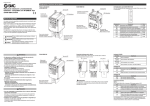
1
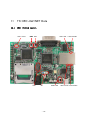
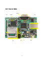
TK-850/JG2+NET
Hardware User’s Manual
TESSERA TECHNOLOGY INC.
June 2008 The 2nd
-1-
edition
Attention
・ The content of this material is a previous notice and might change.
・ The reprint reproduction of this material is prohibited without our approval by the document.
・ Our company doesn't carry the for the mistake of this material at all.
・ Our company doesn't carry the for the violation of the patent, the copyright of the third party
generated in relation to the use of our product published in this material, and other
intellectual property rights etc. at all. Our company doesn't permit our or third party's
patents, copyrights, and other intellectual property rights based on this material.
・ Information that relates to the circuit, software, and these described to this material explains
the operation example and the application example of the semiconductor product.
Please go to design customer's equipment in customer's responsibility when you information
on the circuit, software, and these. Our company doesn't carry the for damage caused in the
customer or the third party who originates in these use at all.
-2-
Table of contents
1
TK-850/JG2+NET .......................................................................................................... 4
1.1
FEATURES ................................................................................................................... 4
1.2
ATTACHED GOODS LIST ............................................................................................... 4
1.3
HARDWARE SPECIFICATION ........................................................................................ 5
2
SWITCHES AND LED .................................................................................................. 6
2.1
SW1 ............................................................................................................................ 6
2.2
SW2,SW3 ................................................................................................................... 9
2.3
SW4 ............................................................................................................................ 9
2.4
LED1,LED2,LED3,LED4.......................................................................................... 9
2.5
LED5 .......................................................................................................................... 9
2.6
LED6~LED8........................................................................................................... 10
2.7
J1.............................................................................................................................. 10
3
NWIRE1 CONNECTOR ...............................................................................................10
4
TERMINAL LIST .........................................................................................................11
5
USB INTERFACE ........................................................................................................12
6
RS-232C CONNECTOR TERMINAL LIST..................................................................12
7
LAN CONTROLLER ....................................................................................................13
7.1
CONNECTION ............................................................................................................ 13
7.2
RESET OF LAN CONTROLLER ................................................................................... 13
7.3
ACCESS TO THE LAN CONTROLLER .......................................................................... 13
8
SD CARD INTERFACE................................................................................................14
9
TEMPERATURE SENSOR ..........................................................................................15
10
OPERATION BY EXTERNAL POWER SUPPLY ....................................................15
11
TK-850/JG2+NET DATA ..........................................................................................16
11.1
LED, SWITCH LAYOUT .............................................................................................. 16
11.2
CONNECTER LAYOUT................................................................................................. 17
11.3
DIMENSION OF THE CPU BOARD .............................................................................. 18
11.4
CIRCUIT DIAGRAM OF THE CPU BOARD ................................................................... 19
-3-
1 TK-850/JG2+NET
V850ES/JG2 is the NEC Electronics 32bit single chip microcomputer.
The features and hardware specification of an evaluation board (TK-850/JG2+NET CPU board) of
V850ES/JG2 are described.
1.1
Features
Features of the TK-850/JG2+NET CPU board are as follows.
●NEC Electronics 32bit single chip microcontroller. (μPD70F3718GC).
All of the ROM, RAM and circumference circuit are efficiently built in one chip on a single board.
●Enable to evaluate applications using mail and HTTP server with Ethernet access as it supports
LAN controller (SMSC LAN9115)
●Lightweight TCP/IP stack that can run on built-in memory from NEC Electronics.
●Easy to use as removable storage and to install OS, as it has SD card interface.
●Enable to make serial communication (1ch) with host PC via USB connection, even the ID-850TK
debugger is in use.
●High speed with built-in 20MHz clock.
●Sub clock 32.768KHz as default.
●The high speed RAM: 40K-byte and the flash memory 512 K-byte are built into CPU chip.
●28 I/O ports are equipped for expand use.
●The board itself is quite and easy to handle; CPU board size: 89mm×69mm.
1.2
Attached goods list
● TK-850/JG2+NET CPU board
● Development tool/Manual CD-ROM
● USB cable (MINI B←→A)
● AC Adapter (DC5V)
-4-
1.3
Hardware specification
Item
CPU
Details
Parts number
μPD70F3718GC-8EA-A
Operation with main clock
20MHz
Clock
Main :5MHz、Sub:32.768KHz
Internal flash memory
512KB
Internal RAM
40KB
Operation voltage
3.3V
I/O voltage
3.3V
USB (MINI B receptacle)
Ethernet (RJ-45 10/100M)
RS-232C (Dsub-9pin plug)
SD Card connecter
Interface
N-Wire connecter (Only SICA pad)
Expansion connecter 30pin (Only pad)
Temperature sensor
AC adapter input connecter
Power supply
5.0V
-5-
2 Switches and LED
2.1
SW1
Bit1~5 of SW 1is dip switch for operation mode setting. Bit6~8 are connected to P79~P711
for multipurpose input .
2.1.1 Please change to the following settings when you use ID850-TK of this product
attachment.
SW1
※
Bit 1
ON
Bit 2
ON
Bit 3
ON
Bit 4
OFF
When ID850-TK is used, these terminals cannot be used because it communicates
with the host machine by using and the terminal P30 and P31.
2.1.2 Please change to the following settings and reset it once when you execute the
program written in the flash memory with built-in CPU without using ID850-TK.
SW1
Bit 1
OFF
Bit 2
OFF
Bit 3
OFF
Bit 4
OFF
-6-
2.1.3 Please change to the following settings when writing it in the flash memory with
built-in CPU by using PG-FPL. (The hardware of PG-FPL is built into TK-850.)
SW1
Bit 1
ON
Bit 2
OFF
Bit 3
ON
Bit 4
ON
2.1.4 Please change to the following settings when you connect N-wire emulator.
SW1
Bit 1
OFF
Bit 2
OFF
Bit 3
OFF
Bit 4
OFF
2.1.5 The Bit5 of SW1 is to switch ON/OFF of RS-232C level converter (MAX3245)
output.
・When you use P90 and P91 port of CN1 extended connector, you need to set the
RS-232C level converter output to OFF by setting Bit5 of SW1 to ON.
・When you use the communication via RS-232C connector, you need to set Bit5 of SW1 to
OFF.
SW1- Bit5
Operation
RS-232C level converter status
ON
Output OFF
OFF
Output ON
:You can set the dotted arrow to off in the following chart.
-7-
MAX3245
MAX3245
CPU
SW1-5
Output OFF signal
D-Sub9Pin
Connecter
P90/TXDA1
RS-232C level
Serial Interface
P91/RXDA1
CN1
Connecter
3.3V level
I/O
2.1.6 Bit6-8 of SW1 is connected with the following terminals CPU.
Connect to GND by switch ON.
It becomes "Low" by switch ON and "High" by switch OFF.
SW1
Bit 6
P79
Bit 7
P710
Bit 8
P711
-8-
2.2
SW2,SW3
SW 2 and SW 3 are push switches. There are connecting to pull-up resister. It becomes
“Low”, while they are being pushed. and It becomes “High” if the switch separate,
SW2,SW3
2.3
Signal
Terminal CPU name at
name
connection destination
SW2
P50
P50/TIQ01/KR0/TOQ01/RTP00
SW3
P51
P51/TIQ02/KR1/TOQ02/RTP01
SW4
SW4 is the reset switch. CPU can be reset by pushing.
2.4
LED1,LED2,LED3,LED4
LED1,2,3 and 4 are available for applications. To make an LED on,
please set the output port LOW.
LED1,LED2,LED3 and LED4
2.5
Signal
Terminal CPU name at
name
connection destination
LED1
PDH0
PDH0/A16
LED2
PDH1
PDH1/A17
LED3
PDH3
PDH3/A18
LED4
PDH2
PDH2/A19
Notes
LED5
`Power LED’. LED5 is activated when the power supply is turned on.
-9-
2.6
LED6~LED8
They show the status of LAN controller.
Displayed Name
Function
LED6
SPEED
Speed Indication
LED7
LINK
Link & Activity
Indication
LED8
2.7
F-DUP
Full-Duplex Indication
J1
It is power supply of CPU.
1-2 Short
It supplies power from USB connected to USB1 connector.
2-3 Short
It supplies power from external AC adapter.
3 NWIRE1 Connector
It is a connector for the N-Wire emulator.
You can connect an emulator such as IE-V850E1-CD-NW.
N-Wire emulator can be connected to NWIRE1 by soldering SICA2P20S (connector from Tokyo
Eletech) and using SICA20I2P (conversion adapter from Tokyo Eletech).
Please do the following setting when you connect N-Wire emulator.
・ Bit1,2, 3, 4 of SW1 are turned off.
- 10 -
4 Terminal list
This is the terminal list for the extended connector CN1 on TK-850/JG2+NET CPU board. CN1 is not
mounted.
CN1 terminal list (HONDA CONNECTORS FFC-30BMEP1:Not mount)
CN1
Signal
name
Terminal CPU name at
connection destination
Notes
1
VDD
VDD
2
P10
P10/ANO0
3
P11
P11/ANO1
4
RESET0
RESET#
5
P02
P02/NMI
6
P03
P03/INTP0/ADTRG
7
P06
P06/INTP3
8
P33
P33/TIP01/TOP01
9
P34
P34/TIP10/TOP10
10
P35
P35/TIP11/TOP11
11
P36
P36
12
P37
P37
13
P90
P90/A0/KR6/TXDA1/SDA02
Connected to TXD of RS232C as well
14
P91
P91/A1/KR7/RXDA1/SCL02
Connected to RXD of RS232C as well
15
P910
P910/A10/SIB3
16
P911
P911/A11/SOB3
17
P912
P912/A12/SCKB3
18
P914
P914/A14/INTP5/TIP51/TOP51
19
P915
P915/A15/INTP6/TIP50/TOP50
20
PCM0
PCM0/WAIT#
21
PCM1
PCM1/CLKOUT
22
PCM2
PCM2/HLDAK
23
PCM3
PCM3/HLDRQ
24
P76
P76/ANI6
25
P75
P75/ANI5
26
P74
P74/ANI4
27
P73
P73/ANI3
28
P72
P72/ANI2
29
P71
P71/ANI1
30
GND
VSS
Connected to NWIRE,RESET circuit
Connected to CTS of RS232C as well
Connected to RTS of RS232C as well
- 11 -
5 USB Interface
When you connect the host PC and USB1 connecter with USB cable, two COM ports exist on the
host PC.
As default, it assigns Ach to smaller number COM port and Bch to larger number COM port.
Ach is used for debugging with ID850-TK and writing programs to the built-in flash memory.
Bch is used for general serial interface for host PC.
USB Interface
Controller
Connect To
A ch
UARTA0
B ch
UARTA2
* For detail about installing USB driver, refer to "USB driver’s install".
6 RS-232C Connector Terminal List
By setting bit5 of SW1 to OFF, you can use RS-232C level serial communication from RS232C1
connector with using UARTA1.
Also, RTS output and CTS input can be used (Active-Low).
RS232C1 Terminal List
Pin No.
Signal
Terminal CPU name at connection
destination
1
N.C.
2
RXD
P91/A1/KR7/RXDA1/SCL02
3
TXD
P90/A0/KR6/TXDA1/SDA02
4
5
Connected to Pin6
GND
GND
6
Connected to Pin4
7
RTS
P35/TIP11/TOP11
8
CTS
P06/INTP3
9
N.C.
Shell
N.C.
- 12 -
7 LAN Controller
LAN9115, LAN controller from SMSC, is mounted on the board. It can use Ethernet communication
complying with IEEE802.3u 100BASE-TX from CN4 connector.
7.1
Connection
Connection between CPU and LAN controller is shown below.
CPU Pin Name
7.2
Signal
Direction
LAN9115 Pin Name
Logic
A2-A8
→
A1-A7
D0-D15
⇔
D0-D15
PCT6
→
nCS
Active-Low
RD (PCT4)
→
nRD
Active-Low
WR0 (PCT0)
→
nWR
Active-Low
P99
→
nRESET
Active-Low
INTP4 (P913)
←
IRQ
Programmable
Reset of LAN Controller
LAN controller can be reset using the P99 port.
7.3
Access to the LAN Controller
It is need to set external bus to separate mode for accessing to the LAN Controller.
LAN controller address is connected to CPU address on the 1bit shift. So LAN controller resister
mapped on skip over 2 Words (4Byte). Also it cannot Byte access to LAN controller, because nBE 0
and nBE1 signal make low level at the same timing.
The Chip Select (AEN, nADS) of LAN controller uses the PCT6 port, Please make the low level
when access to LAN controller. and If access ends, make high level.
- 13 -
8 SD card interface
・For accessing SD card, use CSIB0.
・SD card signal line (CS, DataIn, CLK, DataOut) has buffer circuit for protecting CPU. Set
PDH4 to "Low" to enable the buffer output when accessing SD card.
・You can control the power supply to SD card through P78 port. Set P78 to Low to supply
power to SD card.
・Low level is entered to P04 (INTP1) when SD card is inserted to SD card slot. High level is
entered when SD card is not inserted to SD card slot.
・High level is entered to P77 port when SD card with write-protected ON is inserted to SD
card slot (CN3). Low level is entered to P77 port when SD card with write-protected OFF is
inserted.
Connection about SD card is shown below.
Terminal CPU name
Signal Name
at connection
Function
Logic
destination
CS
PDH5
Chip Select
Active-Low
Data In
SOB0 (P41)
Data Input
Active-High
CLK
SCKB0 (P42)
Clock
Active-High
Data Out
SIB0 (P40)
Data Output
Active-High
CD
INTP1 (P04)
Card Detection
Active-Low
WP
P77
Write-Protect Detection
Active-High
SDOE
PDH4
SD Card Signal Line
Active-Low
SDPO
P78
Effective Output
Output SD Card Power ON
- 14 -
Active-Low
9 Temperature sensor
CPU board has a temperature sensor for measure ambient of PWB board, that is connecting to
analog input pin (P70/ANI0) of CPU
The temperature sensor outputs a voltage depending on the temperature. The temperature can
be retrieved by setting P70 port to A/D converter input.
When the temperature of device is 30℃, the sensor outputs the voltage of about 1.474V. The
changes of voltage on temperature is -8.20mV/℃.
10
・
Temperature sensor S-8120C (Made by SII)
・
Power Supply of sensor :+3.3V
Operation by external power supply
AC adapter can be connected to CN2. When you need to operate the board without connecting
to USB, you can use the power supplied from AC adapter connected to CN2 by setting 2-3Pin
short for the jumper pin (JP1).
Also, you can connect to regulated power supply with lead instead of AC adapter as CN2 is
connected to J1 through-hole.
・Acceptable plug
:2.1mm DC jack (center plus)
・Current capacity
:500mA or more
・Supply voltage
:5V
・J1-1pin:plus
・J1-2pin:minus
- 15 -
11
TK-850/JG2+NET Data
11.1 LED, Switch layout
LED1~LED4
SW2 SW3
SW1
LED7:LINK
JP1
- 16 -
RESET SW
LED5:POWER
LED8:F-DUP LED6:SPEED
11.2 Connecter layout
RS232C1
CN1
NWIRE1
CN3
CN4
CN2
- 17 -
J1
USB1
11.3 Dimension of the CPU Board
- 18 -
1
2
3
2
4
6
8
10
12
14
16
18
20
22
24
26
28
30
NOT MOUNT
FFC-30BMPEP1
1
3
5
7
9
11
13
15
17
19
21
23
25
27
29
C5
10PF
J1
CON1
NOT MOUNT
1
2
P.2
P10
RESET0
P03
P33
P35
P37
P91
P911
P914
PCM0
PCM2
P76
P74
P72
USBVDD
2,3pin=N.C.
4 MC-306 32.7680K-A0
R1
100
XT1
XT2
CSTCR5M00G15
X1
X2
EXT Interface
CN2
HEC0470-01-630
C4
10PF
Y2
3
1
Y1
2
P11
P02
P06
P34
P36
P90
P910
P912
P915
PCM1
PCM3
P75
P73
P71
3
1
2
FFC-3AMEP1
JP1
VDD
1-2:USB
2-3:EXT
FLMD0
SDCD#
+
RESET0
3
I
O
2
U3
LM1117MPX-3.3
VDD
P05
P06
2
1
+
VDD
X1
X2
RESET0
XT1
XT2
P02
P03
FLMD0
P10
P11
0.1uF
C2
VDD
0.1uF
C1
VDD
P.2 RXD0
P.2
C6
10uF/25V
P.3 CTS#
P.3 SDDO
P.3 SDDI
P.3 SDCK
P.3
4.7uF
C3
P.3 SDOE#
P.3 SDCS#
VDD
4
U1
NC
4
AVREF0
AVSS
P10/ANO0
P11/ANO1
AVREF1
PDH4/A20
PDH5/A21
FLMD0
VDD
REGC
VSS
X1
X2
RESET
XT1
XT2
P02/NMI
P03/INTP0/ADTRG
P04/INTP1
P05/INTP2/DRST
P06/INTP3
P40/SIB0/SDA01
P41/SOB0/SCL01
P42/SCKB0
P30/TXDA0/SOB4
3
C7
10uF/25V
P.2
VDD
POWER
LED5
PG1112H
R2
330
P.3 RTS#
TXD0
V850ES/JG2
1
2
3
4
5
6
7
8
9
10
11
12
13
14
15
16
17
18
19
20
21
22
23
24
25
S-8120CNB
VSS
VDD VOUT
P.3
P.3
SDWP
SDPO#
V850ES/JG2
U2
0.1uF
C9
VDD
TP2
VDD
NOT MOUNT
VDD
P.2
P.2
K
PDH3
P.3
P.3
A
0.1uF
C10
D4
D3
D2
D1
D0
0.1uF
C11
A8
PCM3
PCM2
PCM1
PCM0
PDH3
PDH2
P915
P914
P913
P912
P911
P910
A
LED4
SML-311UT
A
LED3
SML-311UT
A
LED2
SML-311UT
D[15..0]
A[8..2]
VDD
P.4
P.4
Date:
Size
A3
Title
LANC_RESET# P.4
P.4
P.4
LANC_WR#
LANC_INT
P.4
P.4
LANC_CS#
LANC_RD#
Monday , April 24, 2006
Document Number
5E1-152A
TK-850/JG2+NET
P53
FLMD0
RESET0
P05
P52
P55
P54
P51
P50
FLMD0
D5
P79
P710
P711
(Shield)
P.3 FOFF#
CN1E4KTTD152J
RN2
VDD
148 Parts, 40 Library Parts, 175 Nets, 684 Pins
+
VDD
RS232
RXD1
TXD1
C8
4.7uF/25V
NOT MOUNT
TP1
GND
USB.B
TXD2
RXD2
K
PDH2
75
74
73
72
71
70
69
68
67
66
65
64
63
62
61
60
59
58
57
56
55
54
53
52
51
K
PDH1
PDL4/AD4
PDL3/AD3
PDL2/AD2
PDL1/AD1
PDL0/AD0
BVDD
BVSS
PCT6/ASTB
PCT4/RD
PCT1/WR1
PCT0/WR0
PCM3/HLDRQ
PCM2/HLDAK
PCM1/CLKOUT
PCM0/WAIT
PDH3/A19
PDH2/A18
P915/A15/INTP6/TIP50/TOP50
P914/A14/INTP5/TIP51/TOP51
P913/A13/INTP4
P912/A12/SCKB3
P911/A11/SOB3
P910/A10/SIB3
P99/A9/SCKB1
P98/A8/SOB1
K
PDH0
LED1
SML-311UT
8
7
6
5
1
2
3
4
TEMP Sensor
FLMD0
P33
P34
P35
P36
P37
CN1
A
K
G TAB
1
P70
P71
P72
P73
P74
P75
P76
P77
P78
P79
P710
P711
PDH1
PDH0
D15
D14
D13
D12
D11
D10
D9
D8
D7
D6
D5
100
99
98
97
96
95
94
93
92
91
90
89
88
87
86
85
84
83
82
81
80
79
78
77
76
P70/ANI0
P71/ANI1
P72/ANI2
P73/ANI3
P74/ANI4
P75/ANI5
P76/ANI6
P77/ANI7
P78/ANI8
P79/ANI9
P710/ANI10
P711/ANI11
PDH1/A17
PDH0/A16
PDL15/AD15
PDL14/AD14
PDL13/AD13
PDL12/AD12
PDL11/AD11
PDL10/AD10
PDL9/AD9
PDL8/AD8
PDL7/AD7
PDL6/AD6
PDL5/AD5/FLMD1
P31/INTP7/RXDA0/SIB4
P32/ASCKA0/SCKB4/TIP00/TOP00
P33/TIP01/TOP01
P34/TIP10/TOP10
P35/TIP11/TOP11
P36
P37
EVSS
EVDD
P38/TXDA2/SDA00
P39/RXDA2/SCL00
P50/TIQ01/TOQ01/RTP00/KR0
P51/TIQ02/TOQ02/RTP01/KR1
P52/TIQ03/TOQ03/RTP02/KR2/DDI
P53/SIB2/TIQ00/RTP03/KR3/DDO/TOQ00
P54/SOB2/RTP04/KR4/DCK
P55/SCKB2/RTP05/KR5/DMS
P90/A0/TXDA1/KR6/SDA2
P91/A1/RXDA1/KR7/SCL02
P92/A2/TIP41/TOP41
P93/A3/TIP40/TOP40
P94/A4/TIP31/TOP31
P95/A5/TIP30/TOP30
P96/A6/TIP21/TOP21
P97/A7/SIB1/TIP20/TOP20
26
27
28
29
30
31
32
33
34
35
36
37
38
39
40
41
42
43
44
45
46
47
48
49
50
P50
P51
P52
P53
P54
P55
P90
P91
A2
A3
A4
A5
A6
A7
P50
2
2
P51
SKQMBB
SW3
SW1-5
12
CHS-08B
5
SKQMBB
SW2
SW1-6
11
CHS-08B
6
Sheet
VDD
1
of
4
Rev
1.0
SICA2P20S
NOT MOUNT
1
2
3
4
5
6
7
8
9
10
11
12
13
14
15
16
17
18
19
20
CN1E4KTTD472J NWIRE1
RN4
VDD
1
1
SW1-7
10
CHS-08B
7
CN1E4KTTD103J
RN3
VDD
SW1-8
9
CHS-08B
8
CN1E4KTTD103J
RN1
VDD
8
7
6
5
1
2
3
4
8
7
6
5
1
2
3
4
8
7
6
5
- 19 -
1
2
3
4
VDD
11.4 Circuit Diagram of the CPU Board
RXD0
1
SW4
P.1
100
VDD
7
5
14
VDD
+
D1
HSK-120
C25
10uF/25V
VDD
R12
100K
VDD
2
1
VDD
2
1
5
P.1
8
6
6
0.1uF
C24
VDD
3
5
VDD
SN74LVC2G06DCK
U6A
U8B
1K
R13
SN74LVC2G14DCK
4
CN1E4KTTD102J
RN5
USBVDD
SN74LVC07APW
U5-4
TXD2 P.1
TXD0
SN74LVC2G14DCK 2
U8A
VDD
7
9
14
VDD
5
SN74LVC07APW
U5-3
6
SN74LVC07APW
4
3
7
U5-2
SN74LVC07APW
2
U5-1
14
VDD
7
1
14
RXD2
R14
1K
VDD
R16
SKQMBB
2
R9
100K
RESET SW
P.1
0.1uF
C14
VDD
1
2
3
4
8
7
6
5
USBVDD
VDD
7
11
14
R4
10K
16
10
R6
10K
SN74LVC07APW
U5-5
R5
10K
CHS-08B
1
SW1-1
26
27
28
29
30
32
33
35
36
37
38
39
40
10
11
12
13
15
16
17
19
20
21
22
23
24
FT2232L
SI/WUB
BCBUS3-TXLED#
BCBUS2-RXLED#
BCBUS1-SLEEP#
BCBUS0-TXDEN
BDBUS7-RI#
BDBUS6-DCD#
BDBUS5-DSR#
BDBUS4-DTR#
BDBUS3-CTS#
BDBUS2-RTS#
BDBUS1-RXD
BDBUS0-TXD
SI/WUA
ACBUS3-TXLED#
ACBUS2-RXLED#
ACBUS1-SLEEP#
ACBUS0-TXDEN
ADBUS7-RI#
ADBUS6-DCD#
ADBUS5-DSR#
ADBUS4-DTR#
ADBUS3-CTS#
ADBUS2-RTS#
ADBUS1-RXD
ADBUS0-TXD
U4
VDD
2
3
5
4
45
9
18
25
34
47
2
1
48
4
44
43
5
7
8
6
31
14
42
3
SN74LVC2G06DCK
U6B
AGND
GND
GND
GND
GND
TEST
EEDATA
EESK
EECS
RESET#
XTOUT
XTIN
RSTOUT#
USBDP
USBDM
3V3OUT
VCC-IOB
VCC-IOA
VCC
VCC
AVCC
46
CHS-08B
14
SW1-3
R11 10K
USBVDD
3
33nF
C15
USBVDD
CSTCR6M00G15
Y3
C12
0.1uF
R10
1.5K
R7
27
R8
27
USBVDD
R3
470
USBVDD
VDD
R15
10K
VDD
2
VDD
USBVDD
L1
C13
4.7uF/25V
4
5
4
2
3
TP3
RESET
Date:
Size
A3
Title
RESET0
GND
ID_NC
DD+
VBUS
13
SW1-4
15
SW1-2
Monday , April 24, 2006
FLMD0
0.1uF
0.1uF
P.1
0.1uF
C23
Sheet
VDD
C22
0.1uF
C20
USBVDD
0.1uF
C19
C21
0.1uF
C18
Document Number
5E1-152A
TK-850/JG2+NET
P.1
CHS-08B
2
CHS-08B
4
0.1uF
C17
0.1uF
C16
USB1
UX60A-MB-5ST
USB Connecter
1
SN74LVC1G126DCK
U7
VDD
BLM41PG750S
+
FG1
FG2
FG3
FG4
FG1
FG2
FG3
FG4
VDD
5
1
3
- 20 -
2
of
4
Rev
1.0
1
RXD1
CTS#
P.1
P.1
RTS#
P.1
2
2
TXD1
2
P.1
C27
0.1uF
R20
100K
2
1
24
28
26
18
19
20
12
13
15
(INTP3) 16
(RXDA1) 17
(P35)
(TXDA1) 14
VDD
0.1uF
1
C31
0.1uF
1
C28
VDD
R5OUT
R4OUT
R3OUT
R2OUT
R1OUT
R2OUTB
T3IN
T2IN
T1IN
C2-
C2+
C1-
C1+
VCC
U9
MAX3245CAI
R5IN
R4IN
R3IN
R2IN
R1IN
T3OUT
T2OUT
T1OUT
INVALID#
FORCEOFF#
FORCEON
V-
V+
GND
8
7
6
5
4
11
10
9
21
22
23
3
27
25
1
0.1uF
2
C29
1
0.1uF
2
C30
SG
DSR
RXD
RTS
TXD
CTS
DTR
P.1
1
6
2
7
3
8
4
9
5
RS232C1
JSEY -9P-5B6L19-13
RS-232C
FOFF#
VDD
(Shield)SDCK
P.1
P.1
P.1
P.1
P.1
SDCS#
SDDI
SDCK
SDOE#
R17
10K VDD
SDPO#
VDD
B1
B2
B3
B4
B5
B6
B7
B8
VCC
GND
18
17
16
15
14
13
12
11
12
SN74LVC07APW
7
U5-6
SDDO
VDDSD
13
14
1
2
20
10
VDD
TC74LCX245FT
A1
A2
A3
A4
A5
A6
A7
A8
OE
DIR
U10
SDPO
2
3
4
5
6
7
8
9
19
1
C26
0.1uF
VDDSD
P.1
VDD
R18
51K
R21
110
2
1
3
Date:
Size
A3
Title
OUT1
4
CLK
9
8
7
6
5
4
3
2
1
CN3
FG2
Monday , April 24, 2006
Document Number
5E1-152A
FG2
FG1
P2
P1
D2
D1
C33
4.7uF/25V
VDDSD
+
P2
P1
D2
D1
FG1
SD CARD
SG5S009V1A1
D2
D1
DOUT
VSS
CLK
VDD
VSS
DIN
CS
TK-850/JG2+NET
VDD
VDDSD
OUT2
G3VM-61G1
K
A
U11
(Shield)CLK
R19
51K
VDDSD VDDSD
VDDSD
8
7
6
5
Sheet
3
of
VDDSD
SDWP
4
Rev
1.0
P.1
SDCD# P.1
SDPO
CN1E4KTTD103J
RN6
C32
0.1uF
1
2
3
4
VDD
1
2
VDD
10
- 21 -
C42
10uF
LANC_INT
LANC_CS#
LANC_WR#
LANC_RD#
LANC_RESET#
C43
0.01uF
PLL1.8
P.1
P.1
P.1
P.1
P.1
P.1 D[15..0]
C44
10uF
R39
1K
VDD
1
VDD
D0
D1
D2
D3
D4
D5
D6
D7
D8
D9
D10
D11
D12
D13
D14
D15
A2
A3
A4
A5
A6
A7
A8
R32
10K
1
2
A[8..2]
C45
0.01uF
CORE1.8
R40
1K
VDD
1
2
70
72
94
93
92
95
29
26
25
24
23
22
75
21
33
32
31
30
40
39
38
37
36
64
63
62
59
58
57
56
53
52
51
50
49
46
45
44
43
18
17
16
15
14
13
12
C46
0.01uF
PME
IRQ
CS#
WR#
RD#
VDD
+
VDDA
C41
10uF/25V
CORE1.8
RESET#
RX_DV
RX_CLK
RX_ER
RXD3
RXD2
RXD1
RXD0
TX_EN
COL
CRS
MDC
MDIO
TX_CLK
TXD0
TXD1
TXD2
TXD3
D0
D1
D2
D3
D4
D5
D6
D7
D8
D9
D10
D11
D12
D13
D14
D15
A1
A2
A3
A4
A5
A6
A7
VDD
2
VREG_3.3
PLL1.8
4
VSS_REF
11
P.1
1
2
1
2
VDD_PLL_1.8
7
VSS_PLL
C47
0.1uF
CORE1.8
65
3
LAN9115
U12
VDD_CORE_1.8
VDD_CORE_1.8
8
VDD_REF_3.3
GND_CORE
GND_CORE
66
1
2
1
2
1
2
1
2
C48
0.1uF
1
2
1
2
GND_I/O
GND_I/O
GND_I/O
GND_I/O
GND_I/O
GND_I/O
GND_I/O
GND_I/O
VDD
C49
0.1uF
19
27
34
41
47
54
60
96
VDD
81
85
89
C50
0.1uF
L2
C51
0.1uF
90
91
73
10
9
5
6
74
76
71
98
99
100
68
69
67
87
83
82
C52
0.1uF
NC
NC
NC
RBIAS
ATEST
XTAL2
XTAL1
SPD_SEL
FIFO_SEL
TESTMODE
GPiO0_LED1#
GPiO0_LED2#
GPiO0_LED3#
EECS
EECLK_GPO4
EEDIO_GPO3
EXRES1
TPI+
TPI-
TPO+
TPO-
79
78
84
BLM18BD121SN1
1
TESTBUSA
VDDA
R27 12.4K(1%)
2
VDD
C53
0.1uF
1
2
C54
0.1uF
2
1
2
3
4
VCC
NC
ORG
VSS
4
3
1
2
CS5032H25.000
GND
X1
X2
GND
Y4
1MΩMount
R NOT MOUNT
M93C46A SN mount
C58
0.1uF
CS
SK
DI
DO
8
7
6
5
2
LED8
PG1112H
A
K
C39
22pF
2
2
LED7
PG1112H
A
LED6
PG1112H
A
C38
0.1uF
VDD
K
K
VDD
C37
0.022uF
R23
51
R24
10
VDDA
R22
51
M93C46-WMN6
6.8nF
2
C35
1
U13
6.8nF
2
C34
1
C40
22pF
C57
0.1uF
2
EECS
EESK
EEDO
EEDI
R34 XXX
2
C56
0.1uF
R38 12K(1%)
2
VDD
1
1
R37 xxx
2
R28 1K
2
2
C36
0.01uF
R26 51
R25 51
R35 1K
C55
0.1uF
1
1
1
1
1
1
2
1
2
1
2
1
2
1
2
20
28
35
42
48
55
61
97
VDD_I/O
VDD_I/O
VDD_I/O
VDD_I/O
VDD_I/O
VDD_I/O
VDD_I/O
VDD_I/O
1
2
1
1
2
VDD_A
VDD_A
VDD_A
VSSA
VSSA
VSSA
VSSA
77
80
86
88
1
2
1
2
1
2
1
2
1
2
1
2
1
2
2
1
2
1
2
2
1
- 22 -
R31
680
R30
680
R29
680
1
1
1
VDD
LAVSS
Date:
Size
A3
Title
F-SUP
LINK
SPEED
8
7
6
5
4
3
2
1
CN4
Monday , April 24, 2006
8
Sheet
LAVSS
TLA-6T707
75Ω
7
6
5
4
3
2
CABLE
1
75Ω 75Ω
Document Number
5E1-152A
TK-850/JG2+NET
0.001uμ
75Ω
RX
TX
1
1
4
R36
0
R33
0
of
2
2
4
Rev
1.0